EP4521878A1 - Semiconductor element manufacturing method and semiconductor element - Google Patents
Semiconductor element manufacturing method and semiconductor element Download PDFInfo
- Publication number
- EP4521878A1 EP4521878A1 EP24798710.0A EP24798710A EP4521878A1 EP 4521878 A1 EP4521878 A1 EP 4521878A1 EP 24798710 A EP24798710 A EP 24798710A EP 4521878 A1 EP4521878 A1 EP 4521878A1
- Authority
- EP
- European Patent Office
- Prior art keywords
- semiconductor device
- film
- manufacturing
- amorphous silicon
- silicide
- Prior art date
- Legal status (The legal status is an assumption and is not a legal conclusion. Google has not performed a legal analysis and makes no representation as to the accuracy of the status listed.)
- Pending
Links
Images










Classifications
-
- H—ELECTRICITY
- H10—SEMICONDUCTOR DEVICES; ELECTRIC SOLID-STATE DEVICES NOT OTHERWISE PROVIDED FOR
- H10B—ELECTRONIC MEMORY DEVICES
- H10B43/00—EEPROM devices comprising charge-trapping gate insulators
- H10B43/20—EEPROM devices comprising charge-trapping gate insulators characterised by three-dimensional [3D] arrangements, e.g. with cells on different height levels
- H10B43/23—EEPROM devices comprising charge-trapping gate insulators characterised by three-dimensional [3D] arrangements, e.g. with cells on different height levels with source and drain on different levels, e.g. with sloping channels
- H10B43/27—EEPROM devices comprising charge-trapping gate insulators characterised by three-dimensional [3D] arrangements, e.g. with cells on different height levels with source and drain on different levels, e.g. with sloping channels the channels comprising vertical portions, e.g. U-shaped channels
-
- H—ELECTRICITY
- H10—SEMICONDUCTOR DEVICES; ELECTRIC SOLID-STATE DEVICES NOT OTHERWISE PROVIDED FOR
- H10B—ELECTRONIC MEMORY DEVICES
- H10B43/00—EEPROM devices comprising charge-trapping gate insulators
- H10B43/30—EEPROM devices comprising charge-trapping gate insulators characterised by the memory core region
- H10B43/35—EEPROM devices comprising charge-trapping gate insulators characterised by the memory core region with cell select transistors, e.g. NAND
-
- H—ELECTRICITY
- H10—SEMICONDUCTOR DEVICES; ELECTRIC SOLID-STATE DEVICES NOT OTHERWISE PROVIDED FOR
- H10D—INORGANIC ELECTRIC SEMICONDUCTOR DEVICES
- H10D30/00—Field-effect transistors [FET]
- H10D30/01—Manufacture or treatment
- H10D30/021—Manufacture or treatment of FETs having insulated gates [IGFET]
- H10D30/031—Manufacture or treatment of FETs having insulated gates [IGFET] of thin-film transistors [TFT]
- H10D30/0312—Manufacture or treatment of FETs having insulated gates [IGFET] of thin-film transistors [TFT] characterised by the gate electrodes
- H10D30/0314—Manufacture or treatment of FETs having insulated gates [IGFET] of thin-film transistors [TFT] characterised by the gate electrodes of lateral top-gate TFTs comprising only a single gate
-
- H—ELECTRICITY
- H10—SEMICONDUCTOR DEVICES; ELECTRIC SOLID-STATE DEVICES NOT OTHERWISE PROVIDED FOR
- H10D—INORGANIC ELECTRIC SEMICONDUCTOR DEVICES
- H10D30/00—Field-effect transistors [FET]
- H10D30/01—Manufacture or treatment
- H10D30/021—Manufacture or treatment of FETs having insulated gates [IGFET]
- H10D30/031—Manufacture or treatment of FETs having insulated gates [IGFET] of thin-film transistors [TFT]
- H10D30/0321—Manufacture or treatment of FETs having insulated gates [IGFET] of thin-film transistors [TFT] comprising silicon, e.g. amorphous silicon or polysilicon
-
- H—ELECTRICITY
- H10—SEMICONDUCTOR DEVICES; ELECTRIC SOLID-STATE DEVICES NOT OTHERWISE PROVIDED FOR
- H10D—INORGANIC ELECTRIC SEMICONDUCTOR DEVICES
- H10D30/00—Field-effect transistors [FET]
- H10D30/60—Insulated-gate field-effect transistors [IGFET]
- H10D30/67—Thin-film transistors [TFT]
- H10D30/6729—Thin-film transistors [TFT] characterised by the electrodes
- H10D30/673—Thin-film transistors [TFT] characterised by the electrodes characterised by the shapes, relative sizes or dispositions of the gate electrodes
- H10D30/6731—Top-gate only TFTs
-
- H—ELECTRICITY
- H10—SEMICONDUCTOR DEVICES; ELECTRIC SOLID-STATE DEVICES NOT OTHERWISE PROVIDED FOR
- H10D—INORGANIC ELECTRIC SEMICONDUCTOR DEVICES
- H10D30/00—Field-effect transistors [FET]
- H10D30/60—Insulated-gate field-effect transistors [IGFET]
- H10D30/67—Thin-film transistors [TFT]
- H10D30/674—Thin-film transistors [TFT] characterised by the active materials
- H10D30/6741—Group IV materials, e.g. germanium or silicon carbide
- H10D30/6743—Silicon
- H10D30/6745—Polycrystalline or microcrystalline silicon
-
- H—ELECTRICITY
- H10—SEMICONDUCTOR DEVICES; ELECTRIC SOLID-STATE DEVICES NOT OTHERWISE PROVIDED FOR
- H10D—INORGANIC ELECTRIC SEMICONDUCTOR DEVICES
- H10D64/00—Electrodes of devices having potential barriers
- H10D64/01—Manufacture or treatment
- H10D64/011—Manufacture or treatment of electrodes ohmically coupled to a semiconductor
- H10D64/0111—Manufacture or treatment of electrodes ohmically coupled to a semiconductor to Group IV semiconductors
- H10D64/0112—Manufacture or treatment of electrodes ohmically coupled to a semiconductor to Group IV semiconductors using conductive layers comprising silicides
-
- H—ELECTRICITY
- H10—SEMICONDUCTOR DEVICES; ELECTRIC SOLID-STATE DEVICES NOT OTHERWISE PROVIDED FOR
- H10D—INORGANIC ELECTRIC SEMICONDUCTOR DEVICES
- H10D86/00—Integrated devices formed in or on insulating or conducting substrates, e.g. formed in silicon-on-insulator [SOI] substrates or on stainless steel or glass substrates
- H10D86/01—Manufacture or treatment
- H10D86/021—Manufacture or treatment of multiple TFTs
- H10D86/0221—Manufacture or treatment of multiple TFTs comprising manufacture, treatment or patterning of TFT semiconductor bodies
- H10D86/0223—Manufacture or treatment of multiple TFTs comprising manufacture, treatment or patterning of TFT semiconductor bodies comprising crystallisation of amorphous, microcrystalline or polycrystalline semiconductor materials
- H10D86/0225—Manufacture or treatment of multiple TFTs comprising manufacture, treatment or patterning of TFT semiconductor bodies comprising crystallisation of amorphous, microcrystalline or polycrystalline semiconductor materials using crystallisation-promoting species, e.g. using a Ni catalyst
-
- H—ELECTRICITY
- H10—SEMICONDUCTOR DEVICES; ELECTRIC SOLID-STATE DEVICES NOT OTHERWISE PROVIDED FOR
- H10P—GENERIC PROCESSES OR APPARATUS FOR THE MANUFACTURE OR TREATMENT OF DEVICES COVERED BY CLASS H10
- H10P14/00—Formation of materials, e.g. in the shape of layers or pillars
- H10P14/20—Formation of materials, e.g. in the shape of layers or pillars of semiconductor materials
- H10P14/34—Deposited materials, e.g. layers
- H10P14/3402—Deposited materials, e.g. layers characterised by the chemical composition
- H10P14/3404—Deposited materials, e.g. layers characterised by the chemical composition being Group IVA materials
- H10P14/3411—Silicon, silicon germanium or germanium
-
- H—ELECTRICITY
- H10—SEMICONDUCTOR DEVICES; ELECTRIC SOLID-STATE DEVICES NOT OTHERWISE PROVIDED FOR
- H10P—GENERIC PROCESSES OR APPARATUS FOR THE MANUFACTURE OR TREATMENT OF DEVICES COVERED BY CLASS H10
- H10P14/00—Formation of materials, e.g. in the shape of layers or pillars
- H10P14/20—Formation of materials, e.g. in the shape of layers or pillars of semiconductor materials
- H10P14/38—Formation of materials, e.g. in the shape of layers or pillars of semiconductor materials characterised by treatments done after the formation of the materials
- H10P14/3802—Crystallisation or recrystallisation of non-monocrystalline semiconductor materials, e.g. regrowth
- H10P14/3806—Crystallisation or recrystallisation of non-monocrystalline semiconductor materials, e.g. regrowth using crystallisation-enhancing elements
-
- H—ELECTRICITY
- H10—SEMICONDUCTOR DEVICES; ELECTRIC SOLID-STATE DEVICES NOT OTHERWISE PROVIDED FOR
- H10P—GENERIC PROCESSES OR APPARATUS FOR THE MANUFACTURE OR TREATMENT OF DEVICES COVERED BY CLASS H10
- H10P95/00—Generic processes or apparatus for manufacture or treatments not covered by the other groups of this subclass
- H10P95/90—Thermal treatments, e.g. annealing or sintering
Definitions
- the present invention relates to a method of manufacturing a semiconductor device, and a semiconductor device.
- a method of single-crystallizing amorphous silicon or polysilicon in a channel As a single crystallization method, there is a MILC (Metal Induced Lateral Crystallization) process in which Ni silicide is used for the growth end of crystallization.
- MILC Metal Induced Lateral Crystallization
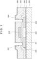
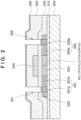
- Figs. 1 to 3 As an example of the MILC process, "Thin-Film Transistor Using Metal Induced Lateral Crystallization Method and Method of Manufacturing the Same" described in PTL 1 will be explained with reference to Figs. 1 to 3 . Referring to Figs.
- reference numeral 200 denotes an insulating substrate; 210, a buffer layer; 220, an active layer; 221 and 225, source/drain regions; 223, a channel region; 230, a gate insulating film; 240, a gate electrode; 250, an interlayer insulating film, 251 and 255, contact holes; and 260, a crystallization induced metal film.
- the interlayer insulating film 250 is deposited on the insulating substrate 200 including the gate electrode 240 to form the contact holes 251 and 255 that expose parts of the source/drain regions 221 and 225.
- the crystallization induced metal film 260 made of Ni or the like is deposited on the insulating substrate 200 by a method such as sputtering.
- an amorphous silicon film of the active layer 220 is crystallized by performing annealing in a furnace, and is changed to a polysilicon film (crystallized at 550°C at a speed of 3 ⁇ m/hr).
- amorphous silicon in lower regions 221a and 225a below the crystallization induced metal film 260 in the contact holes 251 and 255 is crystallized by a Metal Induced Crystallization (MIC) method, and amorphous silicon in remaining regions 221b and 225b is crystallized by the MILC method.
- MIC Metal Induced Crystallization
- the crystallization induced metal film 260 is removed and source/drain electrodes 271 and 275 are formed, thereby obtaining a thin-film transistor.
- PTL 2 discloses a nonvolatile semiconductor storage device that includes a semiconductor substrate, a first layer, a second conductive layer, a memory film, and a semiconductor layer, and includes a metal layer contacting the semiconductor layer and containing Ni, Co, Al, or Pd, in order to make an attempt to relax operation control and circuit layout design while improving an operation speed such as a read speed, a write speed, and a removal speed.
- PTL 2 discloses as follows.
- a portion near a lower end portion of a semiconductor pillar SP may contain an Al alloy and a portion near an upper end portion of the semiconductor pillar SP may contain an Al alloy.
- the semiconductor pillar SP may contain an Al alloy.
- PTL 3 discloses a semiconductor storage device including a first wiring layer, a second wiring layer, and a memory pillar in order to improve processing capability. Furthermore, according to PTL 3, since the lattice parameter of NiSi 2 has a mismatch of only about 0.3% with respect to the lattice parameter of Si, NiSi 2 is suitable for forming single-crystal silicon by the MILC method. It is disclosed that examples of a metal material for crystallizing a semiconductor pillar (for example, silicon, silicon germanium, or germanium) by the MILC method are Ni, Co, Al and Pd.
- NPL 1 relates to the lattice parameter of Si, that of NiSi 2 , and that of NiSi 2-X Al X .
- the abscissa of Fig. 4 represents a ratio X of Al to NiSi 2-X Al X
- a represents the lattice parameter of Si
- the present invention provides a technique of converting amorphous silicon into single-crystal silicon by a silicide having a lattice parameter closer to the lattice parameter of the single-crystal silicon.
- a first aspect of the present invention is related to a method of manufacturing a semiconductor device, including a conversion step of converting amorphous silicon into single-crystal silicon, and in the method of manufacturing, the conversion step includes: a first step of forming a silicide to contact the amorphous silicon by forming, by treatment with heating, a first film containing a first material to cover the amorphous silicon, a second step of forming a compound formed by Si, the first material, and a second material to contact the silicide by forming, by treatment with heating, a second film containing the second material to cover the silicide after the first step, and a third step of changing the silicide remaining after the second step to the compound by annealing, the first material is one material selected from a group consisting of Ni, Pd, Ti, Cu, Pt, Co, Mo, Mg, W, Cr, and Mn, and the second material is one material selected from a group consisting of Al, Au, Sb, In, Ag, and Ga.
- a second aspect of the present invention is related to a method of manufacturing a semiconductor device, including a conversion step of converting amorphous silicon into single-crystal silicon, and in the method of manufacturing, the conversion step includes: a first step of forming a first film containing a first material to cover the amorphous silicon, a second step of forming a second film containing a second material to cover the first film after the first step, and a third step of forming a compound containing Si, the first material, and the second material by annealing after the second step, the first material is one material selected from a group consisting of Ni, Pd, Ti, Cu, Pt, Co, Mo, Mg, W, Cr, and Mn, and the second material is one material selected from a group consisting of Al, Au, Sb, In, Ag, and Ga.
- a third aspect of the present invention is related to a semiconductor device including a stacked structure of amorphous silicon, a compound, and single-crystal silicon, and in the semiconductor device, the compound is a compound of Si, a first material, and a second material, the first material is one material selected from a group consisting of Ni, Pd, Ti, Cu, Pt, Co, Mo, Mg, W, Cr, and Mn, and the second material is one material selected from a group consisting of Al, Au, Sb, In, Ag, and Ga.
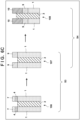
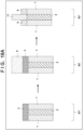
- Figs. 5A to 5C are views schematically showing the first embodiment of a method of manufacturing a semiconductor device, which includes a conversion step of converting amorphous silicon 1 into single-crystal silicon 10. From the result of an experiment of heating a structure obtained by sequentially depositing an Al film and Ni film on amorphous silicon, the present inventor has found that the Al film inhibits silicidation of the Ni film. Furthermore, from the result of an experiment of heating a structure obtained by depositing an NiAl film on amorphous silicon, the present inventor has found that Al is pushed out to the surface side of the NiAl film without being contained in Ni silicide.
- the present inventor has found a phenomenon that when an Ni silicide film contacting amorphous silicon is formed by forming an Ni film on the amorphous silicon by treatment with heating and then an Al film is formed on the Ni silicide film by treatment with heating, Al diffuses in the Ni silicide film to form NiAlSi. Since NiAlSi has a lattice parameter close to that of single-crystal silicon, it is possible to readily obtain single-crystal silicon by performing annealing while NiAlSi is in contact with amorphous silicon. The following embodiments are based on the above knowledge.
- the method of manufacturing the semiconductor device according to the first embodiment can include the conversion step of converting the amorphous silicon 1 into the single-crystal silicon 10.
- the amorphous silicon 1 can form part of a substrate.
- the conversion step can include
- Fig. 5A shows a structure 101 in a state in which the first film 3 containing Ni as the first material is formed by annealing with heating to cover the amorphous silicon 1 in the first step S1, and a structure 102 in which Ni silicide as the silicide 4 is formed.
- Fig. 5B shows a structure 104 in a state in which the second film 6 containing Al as the second material is formed by treatment with heating to cover the silicide 4, and a structure 105 in a state in which NiAlSi as the compound 7 containing Si, Ni (first material), and Al (second material) is formed to contact the silicide 4.
- Fig. 5C shows a structure 106 containing the silicide 4 remaining after the second step S2, and a structure 107 after the silicide 4 changes to the compound 9 by annealing.
- the first material instead of Ni, Pd (palladium), Ti (titanium), Cu (copper), Pt (platinum), Co (cobalt), Mo (molybdenum), Mg (magnesium), W (tungsten), Cr (chromium), or Mn (manganese) may be used. That is, the first material can be one material selected from a group consisting of Ni, Pd, Ti, Cu, Pt, Co, Mo, Mg, W, Cr, and Mn.
- the second material instead of Al, Au (gold), Sb (antimony), In (indium), Ag (silver), or Ga (gallium) may be used. That is, the second material can be one material selected from a group consisting of Al, Au, Sb, In, Ag, and Ga.
- a compound containing Si, the first material, and the second material is preferably, for example, NiAuSi, NiSbSi, NiInSi, NiAgSi, or NiGaSi, instead of NiAlSi.
- the conversion step of converting the amorphous silicon 1 into the single-crystal silicon 10 can further include a fourth step S4 of changing at least part of the amorphous silicon 1 remaining after the third step S3 to the single-crystal silicon 10 by annealing.
- Fig. 5C shows a structure 108 after at least part of the amorphous silicon 1 remaining after the third step S3 changes to the single-crystal silicon 10 by annealing.
- the fourth step can include a MILC (Metal Induced Lateral Crystallization) process.
- the substrate subject to the first step can include an insulating film 2 (for example, SiO 2 : silicon dioxide) in addition to the amorphous silicon 1.
- the amorphous silicon 1 and the insulating film 2 can be arranged to contact each other or close to each other.
- a first material film 3' may be formed to contact the insulating film 2 by forming, by treatment with heating, the first film 3 containing the first material (for example, Ni) to cover the insulating film 2 in addition to the amorphous silicon 1.
- Fig. 5A shows the structure 102 including the first material film 3'.
- the conversion step can further include, between the first step S1 and the second step S2, a step of removing the first material film 3' contacting the insulating film 2 by chemical etching or the like.
- Fig. 5A shows the structure 103 in which the first material film 3' is removed. By removing the first material film 3', it is possible to prevent a situation in which the silicide 4 laterally grows to be associated with another silicide 4 and thus electrical short-circuit occurs.
- a second material film 8 as part of the second film 6 remains in a portion covering the insulating film 2 when forming NiAlSi as the compound 7 containing Si, Ni (first material), and Al (second material) to contact the silicide 4.
- the second material film 8 can be removed after the second step S2 (for example, between the second step S2 and the third step S3).
- a thickness T 2 of the second film 6 formed in the second step S2 (a thickness of the second film 6 in a portion covering the Ni silicide 4) is preferably larger than a thickness T 1 of the first film 3 formed in the first step S1, and smaller than four times the thickness T 1 of the first film 3 formed in the first step S1. That is, 0 ⁇ T 2 ⁇ 4T 1 is preferably satisfied.
- the lattice parameter of NiSi 2-0 Al 0 that is, NiSi 2
- the lattice parameter of NiSi 1.46 Al 0.54 is 5.454.
- the lattice parameter of NiSi 2-X Al X is given by the following expression.
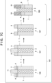
- Figs. 6A to 6C are views schematically showing the second embodiment of a method of manufacturing a semiconductor device, which includes a conversion step of converting amorphous silicon 1 into single-crystal silicon 10. Matters not mentioned as the second embodiment can comply with the first embodiment.
- Fig. 6A schematically shows a first step S1
- Fig. 6B schematically shows a second step S2
- Fig. 6C schematically shows a third step S3 and a fourth step S4.
- a first material film 3' contacting an insulating film 2 is not removed between the first step S1 and the second step S2. Therefore, in the second step S2, by forming, by treatment with heating, a second film 6 containing Al as a second material to cover a silicide 4 and the first material film 3', a second compound 11 of a first material and the second material is obtained to contact the insulating film 2 in addition to a compound 7 contacting the silicide 4.
- the conversion step can include, between the second step S2 and the third step S3, a step of removing the second compound 11 contacting the insulating film 2.
- a step of removing the second compound 11 By removing the second compound 11, it is possible to prevent a situation in which the silicide 4 laterally grows to be associated with another silicide 4 and thus electrical short-circuit occurs.
- Fig. 6B shows a structure 106 in which the second compound 11 is removed.
- Figs. 7A to 7C are views schematically showing the third embodiment of a method of manufacturing a semiconductor device, which includes a conversion step of converting amorphous silicon into single-crystal silicon. Matters not mentioned as the third embodiment can comply with the first embodiment.
- Fig. 7A schematically shows a first step S1
- Fig. 7B schematically shows a second step S2
- Fig. 7C schematically shows a third step S3 and a fourth step S4.
- a first material film 3' contacting an insulating film 2 is not removed between the first step S1 and the second step S2. Therefore, in the second step S2, by forming, by treatment with heating, a second film 6 containing Al as a second material to cover a silicide 4 and the first material film 3', a second compound 11 of a first material and the second material is obtained to contact the insulating film 2 in addition to a compound 7 contacting the silicide 4. In the second embodiment, the second compound 11 contacting the insulating film 2 is not removed between the second step S2 and the third step S3.
- the conversion step can include, after the third step S3 and more specifically between the third step S3 and the fourth step S4, a step of removing the second compound 11 contacting the insulating film 2.
- a step of removing the second compound 11 By removing the second compound 11, it is possible to prevent a situation in which the silicide 4 laterally grows to be associated with another silicide 4 and thus electrical short-circuit occurs.
- Fig. 7C shows a structure 107 in which the second compound 11 is removed.
- the referred drawings show that the first film and the second film are formed on the amorphous silicon 1. These drawings merely show that the first film and the second film are formed on the amorphous silicon 1 in the posture shown in the drawings.
- the formation of the first film and the second film on the amorphous silicon 1 does not limit the present invention to formation of the first film and the second film above the amorphous silicon 1 in a film forming apparatus.
- the formation of the first film and the second film on the amorphous silicon 1 includes formation of the first film and the second film below the amorphous silicon 1 in a film forming apparatus, as exemplified in Figs. 8A to 8C .
- the fourth embodiment of a method of manufacturing a semiconductor device will be described next with reference to Figs. 9 to 17 .
- the fourth embodiment provides a method of manufacturing a semiconductor storage device as an example of the semiconductor device.
- An example of manufacturing a semiconductor storage device including a NAND string will now be described.
- the NAND string includes a plurality of thin-film transistors connected in series.
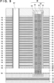
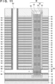
- reference numeral 100 denotes a semiconductor substrate; 111, 114, 116, and 136, insulating films; 112 and 113, wiring layers; 115, a gate electrode layer; 119, a tunnel insulating film; 120, a charge accumulation layer; 121, a block insulating film; 135, amorphous silicon; 123, a core layer; 124A, 124B, and 141, silicide layers; 125, a cap layer; and 136, a conductive layer.
- Reference symbol GP denotes a gap; MP, a memory pillar; and SLT, a slit.
- the gap GP communicates with an external space via the slit SLT.
- the amorphous silicon 135 corresponds to the above-described amorphous silicon 1, and is to be single-crystallized.
- the amorphous silicon 135 is exposed to the gap GP.
- Ni silicide as a silicide 4 is formed to contact the amorphous silicon 135 by forming, by annealing treatment with heating, a first film 3 containing Ni as a first material to cover the amorphous silicon 135.
- a first material film 3' can be formed to contact the insulating film.
- the first material film 3' can be removed thereafter.
- NiAlSi as a compound 7 containing Si, Ni (first material), and Al (second material) is formed to contact the silicide 4 by forming, by treatment with heating, a second film 6 containing Al as the second material to cover the silicide 4.
- a second material film 8 as part of the second film 6 remains in a portion covering the insulating film 136 and the like.
- the second material film 8 on the insulating film is removed.
- the silicide 4 remaining after the second step is changed to an NiAlSi film as a compound 9 containing Si, Ni (first material), and Al (second material) by annealing.
- a fourth step shown in Figs. 16 and 17 at least part of the amorphous silicon 135 remaining after the third step is changed to single-crystal silicon 10 by annealing.
- the fourth embodiment is advantageous in reducing channel resistance that is a problem for a semiconductor storage device (for example, a 3D NAND memory).
- Figs. 18A and 18B are views schematically showing the fifth embodiment of a method of manufacturing a semiconductor device, which includes a conversion step of converting amorphous silicon into single-crystal silicon. Matters not mentioned as the fifth embodiment can comply with the first to third embodiments. The fifth embodiment is applicable to the fourth embodiment.
- the fifth embodiment of the method of manufacturing the semiconductor device can include a conversion step of converting amorphous silicon 1 into single-crystal silicon 10.
- the amorphous silicon 1 can form part of a substrate.
- the conversion step can include a first step S1' of forming a first film 3 containing Ni as a first material to cover the amorphous silicon 1, a second step S2' of forming a second film 6 containing Al as a second material to cover the first film 3 after the first step S1', and a third step S3' of changing the first and second film into an NiAlSi film as a compound 9 containing Si, Ni (first material), and Al (second material) by annealing after the second step S2'.
- the first material instead of Ni, Pd (palladium), Ti (titanium), Cu (copper), Pt (platinum), Co (cobalt), Mo (molybdenum), Mg (magnesium), W (tungsten), Cr (chromium), or Mn (manganese) may be used. That is, the first material can be one material selected from a group consisting of Ni, Pd, Ti, Cu, Pt, Co, Mo, Mg, W, Cr, and Mn.
- the second material instead of Al, Au (gold), Sb (antimony), In (indium), Ag (silver), or Ga (gallium) may be used. That is, the second material can be one material selected from a group consisting of Al, Au, Sb, In, Ag, and Ga.
- a compound containing Si (silicon), Ni (first material), and Al (second material) is preferably, for example, NiAuSi, NiSbSi, NiInSi, NiAgSi, or NiGaSi, instead of NiAlSi.
- the conversion step of converting the amorphous silicon 1 into the single-crystal silicon 10 can further include a fourth step S4' of changing at least part of the amorphous silicon 1 remaining after the third step S3' to the single-crystal silicon 10 by annealing.
- the conversion step may include, between the third step S3' and the fourth step S4', a step of removing a second compound 11 contacting an insulating film 2.
- a stacked structure of the amorphous silicon 1, the compound 9, and the single-crystal silicon 10 is formed via the fourth step S4'.
- the fourth step S4' can include a MILC (Metal Induced Lateral Crystallization) process.
- the thickness of the second film 6 formed in the second step S2' is preferably larger than the thickness of the first film 3 formed in the first step S1', and smaller than four times the thickness of the first film 3 formed in the first step S1'.
- 1 amorphous silicon
- 2 insulating film
- 3 first film (for example, Ni film), 3'; first material film (for example, Ni film), 4: silicide (for example, Ni silicide), 6: second film (for example, Al film), 7: compound (for example, NiAlSi), 8: second material film (for example, Al film), 9: compound (for example, NiAlSi), 10: single-crystal silicon
- 11 second compound (for example, NiAl)
Landscapes
- Electrodes Of Semiconductors (AREA)
- Non-Volatile Memory (AREA)
- Chemical & Material Sciences (AREA)
- Crystallography & Structural Chemistry (AREA)
- Recrystallisation Techniques (AREA)
Abstract
Description
- The present invention relates to a method of manufacturing a semiconductor device, and a semiconductor device.
- As one of methods of solving performance degradation caused by an increase in channel resistance or the like with respect to a semiconductor device (for example, a thin-film transistor or a semiconductor storage device), there is provided a method of single-crystallizing amorphous silicon or polysilicon in a channel. As a single crystallization method, there is a MILC (Metal Induced Lateral Crystallization) process in which Ni silicide is used for the growth end of crystallization. As an example of the MILC process, "Thin-Film Transistor Using Metal Induced Lateral Crystallization Method and Method of Manufacturing the Same" described in
PTL 1 will be explained with reference toFigs. 1 to 3 . Referring toFigs. 1 to 3 ,reference numeral 200 denotes an insulating substrate; 210, a buffer layer; 220, an active layer; 221 and 225, source/drain regions; 223, a channel region; 230, a gate insulating film; 240, a gate electrode; 250, an interlayer insulating film, 251 and 255, contact holes; and 260, a crystallization induced metal film. - As shown in
Fig. 1 , the interlayerinsulating film 250 is deposited on theinsulating substrate 200 including thegate electrode 240 to form thecontact holes drain regions metal film 260 made of Ni or the like is deposited on theinsulating substrate 200 by a method such as sputtering. - Next, as shown in
Fig. 2 , an amorphous silicon film of theactive layer 220 is crystallized by performing annealing in a furnace, and is changed to a polysilicon film (crystallized at 550°C at a speed of 3 µm/hr). At this time, amorphous silicon inlower regions metal film 260 in thecontact holes remaining regions - Next, as shown in
Fig. 3 , the crystallization inducedmetal film 260 is removed and source/drain electrodes -
PTL 2 discloses a nonvolatile semiconductor storage device that includes a semiconductor substrate, a first layer, a second conductive layer, a memory film, and a semiconductor layer, and includes a metal layer contacting the semiconductor layer and containing Ni, Co, Al, or Pd, in order to make an attempt to relax operation control and circuit layout design while improving an operation speed such as a read speed, a write speed, and a removal speed. In addition,PTL 2 discloses as follows. "In a case where the a metal layer 70 is made of a material not forming a silicide, such as Al, after annealing, a portion near a lower end portion of a semiconductor pillar SP may contain an Al alloy and a portion near an upper end portion of the semiconductor pillar SP may contain an Al alloy. Without limitation to the portions near the upper end portion and the lower end portion of the semiconductor pillar SP, the semiconductor pillar SP may contain an Al alloy." -
PTL 3 discloses a semiconductor storage device including a first wiring layer, a second wiring layer, and a memory pillar in order to improve processing capability. Furthermore, according toPTL 3, since the lattice parameter of NiSi2 has a mismatch of only about 0.3% with respect to the lattice parameter of Si, NiSi2 is suitable for forming single-crystal silicon by the MILC method. It is disclosed that examples of a metal material for crystallizing a semiconductor pillar (for example, silicon, silicon germanium, or germanium) by the MILC method are Ni, Co, Al and Pd. - NPL 1 relates to the lattice parameter of Si, that of NiSi2, and that of NiSi2-XAlX. The abscissa of
Fig. 4 represents a ratio X of Al to NiSi2-XAlX, a represents the lattice parameter of Si, and the ordinate ofFig. 4 represents the lattice parameter. It is apparent fromFig. 4 that when the lattice parameter of NiSi2 is 5.406, the lattice parameter of Si is 5.431, and when the ratio X of Al is 0.24, NiSi2-XAlX = 5.431 which matches the lattice parameter of Si. Note that the unit of the lattice parameter inNPL 1 is angstrom, and this specification also assumes that the unit of the lattice parameter is angstrom. -
- PTL 1:
Japanese Patent Laid-Open No. 2005-159307 - PTL 2:
Japanese Patent Laid-Open No. 2014-175348 - PTL 3:
Japanese Patent Laid-Open No. 2019-165178 - NPL 1: Klaus et al. "Appl. Phys. Lett. 83, 497(2003)" pp. 497 - 499
- The present invention provides a technique of converting amorphous silicon into single-crystal silicon by a silicide having a lattice parameter closer to the lattice parameter of the single-crystal silicon.
- A first aspect of the present invention is related to a method of manufacturing a semiconductor device, including a conversion step of converting amorphous silicon into single-crystal silicon, and in the method of manufacturing, the conversion step includes: a first step of forming a silicide to contact the amorphous silicon by forming, by treatment with heating, a first film containing a first material to cover the amorphous silicon, a second step of forming a compound formed by Si, the first material, and a second material to contact the silicide by forming, by treatment with heating, a second film containing the second material to cover the silicide after the first step, and a third step of changing the silicide remaining after the second step to the compound by annealing, the first material is one material selected from a group consisting of Ni, Pd, Ti, Cu, Pt, Co, Mo, Mg, W, Cr, and Mn, and the second material is one material selected from a group consisting of Al, Au, Sb, In, Ag, and Ga.
- A second aspect of the present invention is related to a method of manufacturing a semiconductor device, including a conversion step of converting amorphous silicon into single-crystal silicon, and in the method of manufacturing,
the conversion step includes: a first step of forming a first film containing a first material to cover the amorphous silicon, a second step of forming a second film containing a second material to cover the first film after the first step, and a third step of forming a compound containing Si, the first material, and the second material by annealing after the second step, the first material is one material selected from a group consisting of Ni, Pd, Ti, Cu, Pt, Co, Mo, Mg, W, Cr, and Mn, and the second material is one material selected from a group consisting of Al, Au, Sb, In, Ag, and Ga. - A third aspect of the present invention is related to a semiconductor device including a stacked structure of amorphous silicon, a compound, and single-crystal silicon, and in the semiconductor device, the compound is a compound of Si, a first material, and a second material, the first material is one material selected from a group consisting of Ni, Pd, Ti, Cu, Pt, Co, Mo, Mg, W, Cr, and Mn, and the second material is one material selected from a group consisting of Al, Au, Sb, In, Ag, and Ga.
-
-
Fig. 1 is a process cross-sectional view for explaining a method of manufacturing a thin-film transistor described inPTL 1; -
Fig. 2 is a process cross-sectional view for explaining the method of manufacturing the thin-film transistor described inPTL 1; -
Fig. 3 is a process cross-sectional view for explaining the method of manufacturing the thin-film transistor described inPTL 1; -
Fig. 4 is a graph showing the relationship among the lattice parameter of Si, that of NiSi2, and that of NiSi2-XAlX described inNPL 1; -
Fig. 5A is a process diagram showing a method of manufacturing a semiconductor device according to the first embodiment; -
Fig. 5B is a process diagram showing the method of manufacturing the semiconductor device according to the first embodiment; -
Fig. 5C is a process diagram showing the method of manufacturing the semiconductor device according to the first embodiment; -
Fig. 6A is a process diagram showing a method of manufacturing a semiconductor device according to the second embodiment; -
Fig. 6B is a process diagram showing the method of manufacturing the semiconductor device according to the second embodiment; -
Fig. 6C is a process diagram showing the method of manufacturing the semiconductor device according to the second embodiment; -
Fig. 7A is a process diagram showing a method of manufacturing a semiconductor device according to the third embodiment; -
Fig. 7B is a process diagram showing the method of manufacturing the semiconductor device according to the third embodiment; -
Fig. 7C is a process diagram showing the method of manufacturing the semiconductor device according to the third embodiment; -
Fig. 8A is a process diagram showing the method of manufacturing the semiconductor device according to the first embodiment; -
Fig. 8B is a process diagram showing the method of manufacturing the semiconductor device according to the first embodiment; -
Fig. 8C is a process diagram showing the method of manufacturing the semiconductor device according to the first embodiment; -
Fig. 9 is a process diagram showing a method of manufacturing a semiconductor device according to the fourth embodiment; -
Fig. 10 is a process diagram showing the method of manufacturing the semiconductor device according to the fourth embodiment; -
Fig. 11 is a process diagram showing the method of manufacturing the semiconductor device according to the fourth embodiment; -
Fig. 12 is a process diagram showing the method of manufacturing the semiconductor device according to the fourth embodiment; -
Fig. 13 is a process diagram showing the method of manufacturing the semiconductor device according to the fourth embodiment; -
Fig. 14 is a process diagram showing the method of manufacturing the semiconductor device according to the fourth embodiment; -
Fig. 15 is a process diagram showing the method of manufacturing the semiconductor device according to the fourth embodiment; -
Fig. 16 is a process diagram showing the method of manufacturing the semiconductor device according to the fourth embodiment; -
Fig. 17 is a process diagram showing the method of manufacturing the semiconductor device according to the fourth embodiment; -
Fig. 18A is a process diagram showing a method of manufacturing a semiconductor device according to the fifth embodiment; and -
Fig. 18B is a process diagram showing the method of manufacturing the semiconductor device according to the fifth embodiment. - Hereinafter, embodiments will be described in detail with reference to the attached drawings. Note, the following embodiments are not intended to limit the scope of the claimed invention. Multiple features are described in the embodiments, but limitation is not made to an invention that requires all such features, and multiple such features may be combined as appropriate. Furthermore, in the attached drawings, the same reference numerals are given to the same or similar configurations, and redundant description thereof is omitted.
-
Figs. 5A to 5C are views schematically showing the first embodiment of a method of manufacturing a semiconductor device, which includes a conversion step of convertingamorphous silicon 1 into single-crystal silicon 10. From the result of an experiment of heating a structure obtained by sequentially depositing an Al film and Ni film on amorphous silicon, the present inventor has found that the Al film inhibits silicidation of the Ni film. Furthermore, from the result of an experiment of heating a structure obtained by depositing an NiAl film on amorphous silicon, the present inventor has found that Al is pushed out to the surface side of the NiAl film without being contained in Ni silicide. The present inventor has found a phenomenon that when an Ni silicide film contacting amorphous silicon is formed by forming an Ni film on the amorphous silicon by treatment with heating and then an Al film is formed on the Ni silicide film by treatment with heating, Al diffuses in the Ni silicide film to form NiAlSi. Since NiAlSi has a lattice parameter close to that of single-crystal silicon, it is possible to readily obtain single-crystal silicon by performing annealing while NiAlSi is in contact with amorphous silicon. The following embodiments are based on the above knowledge. - The method of manufacturing the semiconductor device according to the first embodiment can include the conversion step of converting the
amorphous silicon 1 into the single-crystal silicon 10. Theamorphous silicon 1 can form part of a substrate. The conversion step can include - a first step S1 of forming Ni silicide as a
silicide 4 contacting theamorphous silicon 1 by forming, by annealing with heating, afirst film 3 containing Ni (nickel) as a first material to cover theamorphous silicon 1, - a second step S2 of forming NiAlSi as a
compound 7 containing Si (silicon), Ni (first material), and Al (second material) to contact thesilicide 4 by forming, by treatment with heating, asecond film 6 containing Al (aluminum) as the second material to cover thesilicide 4 after the first step S1, and - a third step S3 of changing the
silicide 4 remaining after the second step S2 to an NiAlSi film as acompound 9 containing Si, Ni (first material), and Al (second material) by annealing. - This can create a structure in which NiAlSi as the
compound 9 is arranged to contact theamorphous silicon 1. -
Fig. 5A shows astructure 101 in a state in which thefirst film 3 containing Ni as the first material is formed by annealing with heating to cover theamorphous silicon 1 in the first step S1, and astructure 102 in which Ni silicide as thesilicide 4 is formed.Fig. 5B shows astructure 104 in a state in which thesecond film 6 containing Al as the second material is formed by treatment with heating to cover thesilicide 4, and astructure 105 in a state in which NiAlSi as thecompound 7 containing Si, Ni (first material), and Al (second material) is formed to contact thesilicide 4.Fig. 5C shows astructure 106 containing thesilicide 4 remaining after the second step S2, and astructure 107 after thesilicide 4 changes to thecompound 9 by annealing. - As the first material, instead of Ni, Pd (palladium), Ti (titanium), Cu (copper), Pt (platinum), Co (cobalt), Mo (molybdenum), Mg (magnesium), W (tungsten), Cr (chromium), or Mn (manganese) may be used. That is, the first material can be one material selected from a group consisting of Ni, Pd, Ti, Cu, Pt, Co, Mo, Mg, W, Cr, and Mn.
- As the second material, instead of Al, Au (gold), Sb (antimony), In (indium), Ag (silver), or Ga (gallium) may be used. That is, the second material can be one material selected from a group consisting of Al, Au, Sb, In, Ag, and Ga.
- A compound containing Si, the first material, and the second material is preferably, for example, NiAuSi, NiSbSi, NiInSi, NiAgSi, or NiGaSi, instead of NiAlSi.
- The conversion step of converting the
amorphous silicon 1 into the single-crystal silicon 10 can further include a fourth step S4 of changing at least part of theamorphous silicon 1 remaining after the third step S3 to the single-crystal silicon 10 by annealing.Fig. 5C shows astructure 108 after at least part of theamorphous silicon 1 remaining after the third step S3 changes to the single-crystal silicon 10 by annealing. The fourth step can include a MILC (Metal Induced Lateral Crystallization) process. - The substrate subject to the first step can include an insulating film 2 (for example, SiO2: silicon dioxide) in addition to the
amorphous silicon 1. Theamorphous silicon 1 and the insulatingfilm 2 can be arranged to contact each other or close to each other. In the first step S1, in addition to thesilicide 4 contacting theamorphous silicon 1, a first material film 3' may be formed to contact the insulatingfilm 2 by forming, by treatment with heating, thefirst film 3 containing the first material (for example, Ni) to cover the insulatingfilm 2 in addition to theamorphous silicon 1.Fig. 5A shows thestructure 102 including the first material film 3'. - In this case, the conversion step can further include, between the first step S1 and the second step S2, a step of removing the first material film 3' contacting the insulating
film 2 by chemical etching or the like.Fig. 5A shows thestructure 103 in which the first material film 3' is removed. By removing the first material film 3', it is possible to prevent a situation in which thesilicide 4 laterally grows to be associated with anothersilicide 4 and thus electrical short-circuit occurs. In a case where the first material film 3' contacting the insulatingfilm 2 is removed, in the second step S2, asecond material film 8 as part of thesecond film 6 remains in a portion covering the insulatingfilm 2 when forming NiAlSi as thecompound 7 containing Si, Ni (first material), and Al (second material) to contact thesilicide 4. Thesecond material film 8 can be removed after the second step S2 (for example, between the second step S2 and the third step S3). - A thickness T2 of the
second film 6 formed in the second step S2 (a thickness of thesecond film 6 in a portion covering the Ni silicide 4) is preferably larger than a thickness T1 of thefirst film 3 formed in the first step S1, and smaller than four times the thickness T1 of thefirst film 3 formed in the first step S1. That is, 0 < T2 < 4T1 is preferably satisfied. - T2 = 0 indicates that the value of X on the abscissa of
Fig. 4 is 0. In this case, the lattice parameter of NiSi2-0Al0 (that is, NiSi2) is 5.406. T2 = 4T1 indicates that the value of X on the abscissa ofFig. 4 is 0.54. When the value of X is 0.54, the lattice parameter of NiSi1.46Al0.54 is 5.454. - If 0 < T2 < 4T1 is satisfied, the lattice parameter of NiSi2-XAlX is given by the following expression.
- 5.406 < lattice parameter of NiSi2-XAlX < 5.454
- Therefore, since the lattice parameter of NiSi2-XAlX is close to the lattice parameter of Si = 5.430, as compared with the lattice parameter (5.406) of NiSi2, it is known that this is suitable for forming single-crystal silicon by the MILC process.
- This can reduce channel resistance that is a problem for a semiconductor device such as a thin-film transistor or a semiconductor storage device (for example, a 3D NAND memory).
-
Figs. 6A to 6C are views schematically showing the second embodiment of a method of manufacturing a semiconductor device, which includes a conversion step of convertingamorphous silicon 1 into single-crystal silicon 10. Matters not mentioned as the second embodiment can comply with the first embodiment.Fig. 6A schematically shows a first step S1,Fig. 6B schematically shows a second step S2, andFig. 6C schematically shows a third step S3 and a fourth step S4. - In the second embodiment, a first material film 3' contacting an insulating
film 2 is not removed between the first step S1 and the second step S2. Therefore, in the second step S2, by forming, by treatment with heating, asecond film 6 containing Al as a second material to cover asilicide 4 and the first material film 3', asecond compound 11 of a first material and the second material is obtained to contact the insulatingfilm 2 in addition to acompound 7 contacting thesilicide 4. - In the second embodiment, the conversion step can include, between the second step S2 and the third step S3, a step of removing the
second compound 11 contacting the insulatingfilm 2. By removing thesecond compound 11, it is possible to prevent a situation in which thesilicide 4 laterally grows to be associated with anothersilicide 4 and thus electrical short-circuit occurs.Fig. 6B shows astructure 106 in which thesecond compound 11 is removed. -
Figs. 7A to 7C are views schematically showing the third embodiment of a method of manufacturing a semiconductor device, which includes a conversion step of converting amorphous silicon into single-crystal silicon. Matters not mentioned as the third embodiment can comply with the first embodiment.Fig. 7A schematically shows a first step S1,Fig. 7B schematically shows a second step S2, andFig. 7C schematically shows a third step S3 and a fourth step S4. - In the third embodiment, a first material film 3' contacting an insulating
film 2 is not removed between the first step S1 and the second step S2. Therefore, in the second step S2, by forming, by treatment with heating, asecond film 6 containing Al as a second material to cover asilicide 4 and the first material film 3', asecond compound 11 of a first material and the second material is obtained to contact the insulatingfilm 2 in addition to acompound 7 contacting thesilicide 4. In the second embodiment, thesecond compound 11 contacting the insulatingfilm 2 is not removed between the second step S2 and the third step S3. - In the third embodiment, the conversion step can include, after the third step S3 and more specifically between the third step S3 and the fourth step S4, a step of removing the
second compound 11 contacting the insulatingfilm 2. By removing thesecond compound 11, it is possible to prevent a situation in which thesilicide 4 laterally grows to be associated with anothersilicide 4 and thus electrical short-circuit occurs.Fig. 7C shows astructure 107 in which thesecond compound 11 is removed. - In each of the first to third embodiments, the referred drawings show that the first film and the second film are formed on the
amorphous silicon 1. These drawings merely show that the first film and the second film are formed on theamorphous silicon 1 in the posture shown in the drawings. The formation of the first film and the second film on theamorphous silicon 1 does not limit the present invention to formation of the first film and the second film above theamorphous silicon 1 in a film forming apparatus. The formation of the first film and the second film on theamorphous silicon 1 includes formation of the first film and the second film below theamorphous silicon 1 in a film forming apparatus, as exemplified inFigs. 8A to 8C . - The fourth embodiment of a method of manufacturing a semiconductor device will be described next with reference to
Figs. 9 to 17 . The fourth embodiment provides a method of manufacturing a semiconductor storage device as an example of the semiconductor device. An example of manufacturing a semiconductor storage device including a NAND string will now be described. The NAND string includes a plurality of thin-film transistors connected in series. - Referring to
Figs. 9 to 17 ,reference numeral 100 denotes a semiconductor substrate; 111, 114, 116, and 136, insulating films; 112 and 113, wiring layers; 115, a gate electrode layer; 119, a tunnel insulating film; 120, a charge accumulation layer; 121, a block insulating film; 135, amorphous silicon; 123, a core layer; 124A, 124B, and 141, silicide layers; 125, a cap layer; and 136, a conductive layer. Reference symbol GP denotes a gap; MP, a memory pillar; and SLT, a slit. - In a state shown in
Fig. 9 , the gap GP communicates with an external space via the slit SLT. Theamorphous silicon 135 corresponds to the above-describedamorphous silicon 1, and is to be single-crystallized. Theamorphous silicon 135 is exposed to the gap GP. In this state, in a first step shown inFigs. 10 and11 , Ni silicide as asilicide 4 is formed to contact theamorphous silicon 135 by forming, by annealing treatment with heating, afirst film 3 containing Ni as a first material to cover theamorphous silicon 135. At this time, in addition to thesilicide 4 contacting theamorphous silicon 135, a first material film 3' can be formed to contact the insulating film. The first material film 3' can be removed thereafter. - Next, in a second step shown in
Figs. 12 and13 , NiAlSi as acompound 7 containing Si, Ni (first material), and Al (second material) is formed to contact thesilicide 4 by forming, by treatment with heating, asecond film 6 containing Al as the second material to cover thesilicide 4. At this time, asecond material film 8 as part of thesecond film 6 remains in a portion covering the insulatingfilm 136 and the like. - Next, in an arbitrary step shown in
Fig. 14 , thesecond material film 8 on the insulating film is removed. Next, in a third step shown inFig. 15 , thesilicide 4 remaining after the second step is changed to an NiAlSi film as acompound 9 containing Si, Ni (first material), and Al (second material) by annealing. - Next, in a fourth step shown in
Figs. 16 and17 , at least part of theamorphous silicon 135 remaining after the third step is changed to single-crystal silicon 10 by annealing. The fourth embodiment is advantageous in reducing channel resistance that is a problem for a semiconductor storage device (for example, a 3D NAND memory). -
Figs. 18A and18B are views schematically showing the fifth embodiment of a method of manufacturing a semiconductor device, which includes a conversion step of converting amorphous silicon into single-crystal silicon. Matters not mentioned as the fifth embodiment can comply with the first to third embodiments. The fifth embodiment is applicable to the fourth embodiment. - The fifth embodiment of the method of manufacturing the semiconductor device can include a conversion step of converting
amorphous silicon 1 into single-crystal silicon 10. Theamorphous silicon 1 can form part of a substrate. The conversion step can include a first step S1' of forming afirst film 3 containing Ni as a first material to cover theamorphous silicon 1, a second step S2' of forming asecond film 6 containing Al as a second material to cover thefirst film 3 after the first step S1', and a third step S3' of changing the first and second film into an NiAlSi film as acompound 9 containing Si, Ni (first material), and Al (second material) by annealing after the second step S2'. - This can create a structure in which NiAlSi as the
compound 9 is arranged to contact theamorphous silicon 1. - As the first material, instead of Ni, Pd (palladium), Ti (titanium), Cu (copper), Pt (platinum), Co (cobalt), Mo (molybdenum), Mg (magnesium), W (tungsten), Cr (chromium), or Mn (manganese) may be used. That is, the first material can be one material selected from a group consisting of Ni, Pd, Ti, Cu, Pt, Co, Mo, Mg, W, Cr, and Mn.
- As the second material, instead of Al, Au (gold), Sb (antimony), In (indium), Ag (silver), or Ga (gallium) may be used. That is, the second material can be one material selected from a group consisting of Al, Au, Sb, In, Ag, and Ga.
- A compound containing Si (silicon), Ni (first material), and Al (second material) is preferably, for example, NiAuSi, NiSbSi, NiInSi, NiAgSi, or NiGaSi, instead of NiAlSi.
- The conversion step of converting the
amorphous silicon 1 into the single-crystal silicon 10 can further include a fourth step S4' of changing at least part of theamorphous silicon 1 remaining after the third step S3' to the single-crystal silicon 10 by annealing. The conversion step may include, between the third step S3' and the fourth step S4', a step of removing asecond compound 11 contacting an insulatingfilm 2. - A stacked structure of the
amorphous silicon 1, thecompound 9, and the single-crystal silicon 10 is formed via the fourth step S4'. The fourth step S4' can include a MILC (Metal Induced Lateral Crystallization) process. The thickness of thesecond film 6 formed in the second step S2' is preferably larger than the thickness of thefirst film 3 formed in the first step S1', and smaller than four times the thickness of thefirst film 3 formed in the first step S1'. - The present invention is not limited to the above embodiments and various changes and modifications can be made within the spirit and scope of the present invention. Therefore, to apprise the public of the scope of the present invention, the following claims are made.
- 1: amorphous silicon, 2: insulating film, 3: first film (for example, Ni film), 3'; first material film (for example, Ni film), 4: silicide (for example, Ni silicide), 6: second film (for example, Al film), 7: compound (for example, NiAlSi), 8: second material film (for example, Al film), 9: compound (for example, NiAlSi), 10: single-crystal silicon, 11: second compound (for example, NiAl)
Claims (28)
- A method of manufacturing a semiconductor device, including a conversion step of converting amorphous silicon into single-crystal silicon, wherein
the conversion step includes:a first step of forming a silicide to contact the amorphous silicon by forming, by treatment with heating, a first film containing a first material to cover the amorphous silicon,a second step of forming a compound formed by Si, the first material, and a second material to contact the silicide by forming, by treatment with heating, a second film containing the second material to cover the silicide after the first step, anda third step of changing the silicide remaining after the second step to the compound by annealing,the first material is one material selected from a group consisting of Ni, Pd, Ti, Cu, Pt, Co, Mo, Mg, W, Cr, and Mn, andthe second material is one material selected from a group consisting of Al, Au, Sb, In, Ag, and Ga. - The method of manufacturing the semiconductor device, according to claim 1, wherein
the conversion step further includes a fourth step of changing at least part of the amorphous silicon remaining after the third step to a single-crystal silicon by annealing. - The method of manufacturing the semiconductor device, according to claim 2, wherein
a stacked structure of the amorphous silicon, the compound, and the single-crystal silicon is formed via the fourth step. - The method of manufacturing the semiconductor device, according to claim 3, wherein
the fourth step includes a MILC (Metal Induced Lateral Crystallization) process. - The method of manufacturing the semiconductor device, according to any one of claims 1 to 4, wherein
a thickness of the second film formed in the second step is larger than a thickness of the first film formed in the first step, and is smaller than four times the thickness of the first film formed in the first step. - The method of manufacturing the semiconductor device, according to any one of claims 1 to 5, wherein
the second material is Al. - The method of manufacturing the semiconductor device, according to any one of claims 1 to 5, wherein
the first material is Ni. - The method of manufacturing the semiconductor device, according to any one of claims 1 to 5, wherein
the first material is Ni and the second material is Al. - The method of manufacturing the semiconductor device, according to any one of claims 1 to 4, wherein
in the first step, a first material film contacting an insulating film is formed in addition to the silicide contacting the amorphous silicon by forming, by treatment with heating, the first film containing the first material to cover the insulating film in addition to the amorphous silicon. - The method of manufacturing the semiconductor device, according to claim 9, wherein
the conversion step further includes, between the first step and the second step, a step of removing the first material film contacting the insulating film. - The method of manufacturing the semiconductor device, according to claim 10, wherein
in the second step, a second material film contacting the insulating film is formed in addition to the compound contacting the silicide by forming, by treatment with heating, the second film containing the first material to cover the insulating film in addition to the silicide. - The method of manufacturing the semiconductor device, according to claim 11, wherein
the conversion step further includes, between the second step and the third step, a step of removing the second material film contacting the insulating film. - The method of manufacturing the semiconductor device, according to claim 9, wherein
in the second step, a second compound of the first material and the second material, contacting the insulating film, is obtained in addition to the compound contacting the silicide by forming, by treatment with heating, the second film containing the second material to cover the silicide and the first material film. - The method of manufacturing the semiconductor device, according to claim 13, wherein
the conversion step includes, between the second step and the third step, a step of removing the second compound contacting the insulating film. - The method of manufacturing the semiconductor device, according to claim 13, wherein
the conversion step further includes, after the third step, a step of removing the second compound contacting the insulating film. - A semiconductor device containing single-crystal silicon created by a method of manufacturing a semiconductor device, defined in any one of claims 1 to 15.
- The semiconductor device according to claim 16, wherein the single-crystal silicon forms part of one of a thin-film transistor and a semiconductor storage device.
- A method of manufacturing a semiconductor device, including a conversion step of converting amorphous silicon into single-crystal silicon, wherein
the conversion step includes:a first step of forming a first film containing a first material to cover the amorphous silicon,a second step of forming a second film containing a second material to cover the first film after the first step, anda third step of forming a compound containing Si, the first material, and the second material by annealing after the second step,the first material is one material selected from a group consisting of Ni, Pd, Ti, Cu, Pt, Co, Mo, Mg, W, Cr, and Mn, andthe second material is one material selected from a group consisting of Al, Au, Sb, In, Ag, and Ga. - The method of manufacturing the semiconductor device, according to claim 18, wherein
the conversion step further includes a fourth step of changing at least part of the amorphous silicon remaining after the third step to a single-crystal silicon by annealing. - The method of manufacturing the semiconductor device, according to claim 19, wherein
a stacked structure of the amorphous silicon, the compound, and the single-crystal silicon is formed via the fourth step. - The method of manufacturing the semiconductor device, according to claim 20, wherein
the fourth step includes a MILC (Metal Induced Lateral Crystallization) process. - The method of manufacturing the semiconductor device, according to any one of claims 18 to 21, wherein
a thickness of the second film formed in the second step is larger than a thickness of the first film formed in the first step, and is smaller than four times the thickness of the first film formed in the first step. - The method of manufacturing the semiconductor device, according to any one of claims 18 to 22, wherein
the second material is Al. - The method of manufacturing the semiconductor device, according to any one of claims 18 to 22, wherein
the first material is Ni. - The method of manufacturing the semiconductor device, according to any one of claims 18 to 22, wherein
the first material is Ni and the second material is Al. - A semiconductor device containing single-crystal silicon created by a method of manufacturing a semiconductor device, defined in any one of claims 18 to 25.
- The semiconductor device according to claim 26, wherein the single-crystal silicon forms part of one of a thin-film transistor and a semiconductor storage device.
- A semiconductor device including a stacked structure of amorphous silicon, a compound, and single-crystal silicon, whereinthe compound is a compound of Si, a first material, and a second material,the first material is one material selected from a group consisting of Ni, Pd, Ti, Cu, Pt, Co, Mo, Mg, W, Cr, and Mn, andthe second material is one material selected from a group consisting of Al, Au, Sb, In, Ag, and Ga.
Applications Claiming Priority (2)
| Application Number | Priority Date | Filing Date | Title |
|---|---|---|---|
| JP2023115732 | 2023-07-14 | ||
| PCT/JP2024/014280 WO2025017981A1 (en) | 2023-07-14 | 2024-04-08 | Semiconductor element manufacturing method and semiconductor element |
Publications (2)
| Publication Number | Publication Date |
|---|---|
| EP4521878A1 true EP4521878A1 (en) | 2025-03-12 |
| EP4521878A4 EP4521878A4 (en) | 2026-04-29 |
Family
ID=94281866
Family Applications (1)
| Application Number | Title | Priority Date | Filing Date |
|---|---|---|---|
| EP24798710.0A Pending EP4521878A4 (en) | 2023-07-14 | 2024-04-08 | METHOD FOR MANUFACTURING A SEMICONDUCTOR COMPONENT AND SEMICONDUCTOR COMPONENT |
Country Status (7)
| Country | Link |
|---|---|
| US (1) | US20250081500A1 (en) |
| EP (1) | EP4521878A4 (en) |
| JP (1) | JP7659708B1 (en) |
| KR (2) | KR102835288B1 (en) |
| CN (1) | CN119654979A (en) |
| TW (1) | TWI910617B (en) |
| WO (1) | WO2025017981A1 (en) |
Families Citing this family (1)
| Publication number | Priority date | Publication date | Assignee | Title |
|---|---|---|---|---|
| CN120711792B (en) * | 2025-08-12 | 2025-12-16 | 合肥晶合集成电路股份有限公司 | Semiconductor devices and their manufacturing methods |
Family Cites Families (19)
| Publication number | Priority date | Publication date | Assignee | Title |
|---|---|---|---|---|
| KR100390523B1 (en) * | 2001-01-20 | 2003-07-04 | 주승기 | Method for crystallizing silicone layer |
| KR100611744B1 (en) | 2003-11-22 | 2006-08-10 | 삼성에스디아이 주식회사 | Thin film transistor using metal induced lateral crystallization and its manufacturing method |
| KR100623228B1 (en) * | 2003-11-27 | 2006-09-18 | 삼성에스디아이 주식회사 | A thin film transistor, an organic light emitting display device having the thin film transistor, and a manufacturing method of the thin film transistor |
| JP2007251030A (en) * | 2006-03-17 | 2007-09-27 | Renesas Technology Corp | Semiconductor device manufacturing method and semiconductor device |
| TWI392092B (en) * | 2008-11-10 | 2013-04-01 | 國立中山大學 | Semiconductor device with π-type semiconductor conduction layer and method of fabricating the same |
| CN102709184B (en) * | 2011-05-13 | 2016-08-17 | 京东方科技集团股份有限公司 | Thin film transistor (TFT), its manufacture method and array base palte containing polysilicon active layer |
| JP2014175348A (en) | 2013-03-06 | 2014-09-22 | Toshiba Corp | Non-volatile semiconductor memory |
| JP2014179465A (en) * | 2013-03-14 | 2014-09-25 | Toshiba Corp | Nonvolatile semiconductor storage device and manufacturing method of the same |
| CN105244414B (en) * | 2015-10-20 | 2017-04-12 | 华中科技大学 | Molybdenum disulfide / silicon heterojunction solar energy cell and preparation method thereof |
| US9780103B2 (en) * | 2015-11-16 | 2017-10-03 | Micron Technology, Inc. | Methods of forming integrated structures |
| JP2017174860A (en) * | 2016-03-18 | 2017-09-28 | 東芝メモリ株式会社 | Semiconductor memory device and manufacturing method thereof |
| CN108022934A (en) * | 2016-11-01 | 2018-05-11 | 沈阳硅基科技有限公司 | A kind of preparation method of film |
| WO2018109552A1 (en) * | 2016-12-15 | 2018-06-21 | Asm Ip Holding B.V. | Semiconductor processing apparatus |
| JP2018157069A (en) * | 2017-03-17 | 2018-10-04 | 東芝メモリ株式会社 | Semiconductor memory device |
| JP7013295B2 (en) * | 2018-03-20 | 2022-01-31 | キオクシア株式会社 | Semiconductor storage device |
| JP7371507B2 (en) * | 2020-01-22 | 2023-10-31 | 富士電機株式会社 | Method for manufacturing silicon carbide semiconductor device |
| FR3106932B1 (en) * | 2020-02-04 | 2023-10-27 | Commissariat Energie Atomique | METHOD FOR MANUFACTURING A STRUCTURED SUBSTRATE |
| CN112786614B (en) | 2021-03-22 | 2022-04-29 | 长江存储科技有限责任公司 | Method for preparing three-dimensional memory |
| CN115548140A (en) * | 2022-10-20 | 2022-12-30 | 中建材浚鑫科技有限公司 | Metallized heterojunction battery and preparation method thereof |
-
2024
- 2024-04-08 WO PCT/JP2024/014280 patent/WO2025017981A1/en not_active Ceased
- 2024-04-08 KR KR1020247028711A patent/KR102835288B1/en active Active
- 2024-04-08 CN CN202480002783.9A patent/CN119654979A/en active Pending
- 2024-04-08 KR KR1020257023267A patent/KR102936129B1/en active Active
- 2024-04-08 JP JP2024554238A patent/JP7659708B1/en active Active
- 2024-04-08 EP EP24798710.0A patent/EP4521878A4/en active Pending
- 2024-04-25 TW TW113115473A patent/TWI910617B/en active
- 2024-11-11 US US18/943,526 patent/US20250081500A1/en active Pending
Also Published As
| Publication number | Publication date |
|---|---|
| KR102835288B1 (en) | 2025-07-18 |
| WO2025017981A1 (en) | 2025-01-23 |
| US20250081500A1 (en) | 2025-03-06 |
| KR102936129B1 (en) | 2026-03-09 |
| KR20250111390A (en) | 2025-07-22 |
| KR20250013142A (en) | 2025-01-31 |
| JP7659708B1 (en) | 2025-04-09 |
| CN119654979A (en) | 2025-03-18 |
| JPWO2025017981A1 (en) | 2025-01-23 |
| TWI910617B (en) | 2026-01-01 |
| TW202519029A (en) | 2025-05-01 |
| EP4521878A4 (en) | 2026-04-29 |
Similar Documents
| Publication | Publication Date | Title |
|---|---|---|
| CN112789724B (en) | Covering layer for bit line resistance reduction | |
| US11107823B2 (en) | Integrated structures and methods of forming integrated structures | |
| JP5497324B2 (en) | Polycrystalline silicon manufacturing method, thin film transistor, manufacturing method thereof, and organic light emitting display device including the same | |
| JP2008311649A (en) | THIN FILM TRANSISTOR, ITS MANUFACTURING METHOD, AND ORGANIC ELECTROLUMINESCENT DISPLAY DEVICE INCLUDING THE SAME | |
| JP2010206196A (en) | Thin-film transistor, manufacturing method thereof, and organic electroluminescence display device including the same | |
| US20250081500A1 (en) | Method of manufacturing semiconductor device and semiconductor device | |
| TWI686934B (en) | Semiconductor memory device | |
| WO2020076758A1 (en) | Devices including vertical transistors having hydrogen barrier materials, and related methods | |
| JP2009182264A (en) | Semiconductor device and manufacturing method thereof | |
| TW200908338A (en) | Method to form low-defect polycrystalline semiconductor material for use in a transistor | |
| JP6367167B2 (en) | Semiconductor device | |
| JP2025160222A (en) | Polysilicon-based word lines for 3D memories | |
| JP6376736B2 (en) | Semiconductor device and manufacturing method thereof | |
| JP2007214436A (en) | Semiconductor device manufacturing method and semiconductor device | |
| US20060040434A1 (en) | Method of fabricating thin film transistor | |
| US20260080909A1 (en) | Semiconductor memory device and method of manufacturing the same | |
| US20230352296A1 (en) | Structure and formation method of device with ferroelectric layer | |
| KR102717752B1 (en) | Silicon-containing layer for reducing bit line resistance | |
| KR20070028121A (en) | Thin film transistor | |
| US20220352176A1 (en) | Method to scale dram with self aligned bit line process | |
| CN121463449A (en) | Semiconductor device, method of manufacturing the same, and electronic apparatus | |
| CN121888589A (en) | Semiconductor device, method of manufacturing the same, and electronic apparatus | |
| US20080233703A1 (en) | Polysilicon conductivity improvement in a salicide process technology | |
| JP2010177358A (en) | Method for manufacturing semiconductor device |
Legal Events
| Date | Code | Title | Description |
|---|---|---|---|
| STAA | Information on the status of an ep patent application or granted ep patent |
Free format text: STATUS: UNKNOWN |
|
| STAA | Information on the status of an ep patent application or granted ep patent |
Free format text: STATUS: THE INTERNATIONAL PUBLICATION HAS BEEN MADE |
|
| PUAI | Public reference made under article 153(3) epc to a published international application that has entered the european phase |
Free format text: ORIGINAL CODE: 0009012 |
|
| STAA | Information on the status of an ep patent application or granted ep patent |
Free format text: STATUS: REQUEST FOR EXAMINATION WAS MADE |
|
| 17P | Request for examination filed |
Effective date: 20241106 |
|
| AK | Designated contracting states |
Kind code of ref document: A1 Designated state(s): AL AT BE BG CH CY CZ DE DK EE ES FI FR GB GR HR HU IE IS IT LI LT LU LV MC ME MK MT NL NO PL PT RO RS SE SI SK SM TR |
|
| A4 | Supplementary search report drawn up and despatched |
Effective date: 20260330 |
|
| RIC1 | Information provided on ipc code assigned before grant |
Ipc: H10B 43/27 20230101AFI20260324BHEP Ipc: H10D 30/01 20250101ALI20260324BHEP Ipc: H10D 30/67 20250101ALI20260324BHEP Ipc: H10D 30/68 20250101ALI20260324BHEP Ipc: H10D 30/69 20250101ALI20260324BHEP Ipc: H10B 41/27 20230101ALI20260324BHEP Ipc: H10D 64/01 20250101ALI20260324BHEP Ipc: H10D 86/01 20250101ALI20260324BHEP Ipc: H10P 14/20 20260101ALI20260324BHEP |