EP4521624A1 - Power conversion device - Google Patents
Power conversion device Download PDFInfo
- Publication number
- EP4521624A1 EP4521624A1 EP22940823.2A EP22940823A EP4521624A1 EP 4521624 A1 EP4521624 A1 EP 4521624A1 EP 22940823 A EP22940823 A EP 22940823A EP 4521624 A1 EP4521624 A1 EP 4521624A1
- Authority
- EP
- European Patent Office
- Prior art keywords
- value
- arm
- voltage
- balance
- control unit
- Prior art date
- Legal status (The legal status is an assumption and is not a legal conclusion. Google has not performed a legal analysis and makes no representation as to the accuracy of the status listed.)
- Pending
Links
Images






Classifications
-
- H—ELECTRICITY
- H02—GENERATION; CONVERSION OR DISTRIBUTION OF ELECTRIC POWER
- H02M—APPARATUS FOR CONVERSION BETWEEN AC AND AC, BETWEEN AC AND DC, OR BETWEEN DC AND DC, AND FOR USE WITH MAINS OR SIMILAR POWER SUPPLY SYSTEMS; CONVERSION OF DC OR AC INPUT POWER INTO SURGE OUTPUT POWER; CONTROL OR REGULATION THEREOF
- H02M7/00—Conversion of AC power input into DC power output; Conversion of DC power input into AC power output
- H02M7/42—Conversion of DC power input into AC power output without possibility of reversal
- H02M7/44—Conversion of DC power input into AC power output without possibility of reversal by static converters
- H02M7/48—Conversion of DC power input into AC power output without possibility of reversal by static converters using discharge tubes with control electrode or semiconductor devices with control electrode
- H02M7/483—Converters with outputs that each can have more than two voltages levels
- H02M7/4835—Converters with outputs that each can have more than two voltages levels comprising two or more cells, each including a switchable capacitor, the capacitors having a nominal charge voltage which corresponds to a given fraction of the input voltage, and the capacitors being selectively connected in series to determine the instantaneous output voltage
-
- H—ELECTRICITY
- H02—GENERATION; CONVERSION OR DISTRIBUTION OF ELECTRIC POWER
- H02M—APPARATUS FOR CONVERSION BETWEEN AC AND AC, BETWEEN AC AND DC, OR BETWEEN DC AND DC, AND FOR USE WITH MAINS OR SIMILAR POWER SUPPLY SYSTEMS; CONVERSION OF DC OR AC INPUT POWER INTO SURGE OUTPUT POWER; CONTROL OR REGULATION THEREOF
- H02M1/00—Details of apparatus for conversion
- H02M1/0003—Details of control, feedback or regulation circuits
- H02M1/0025—Arrangements for modifying reference values, feedback values or error values in the control loop of a converter
-
- H—ELECTRICITY
- H02—GENERATION; CONVERSION OR DISTRIBUTION OF ELECTRIC POWER
- H02M—APPARATUS FOR CONVERSION BETWEEN AC AND AC, BETWEEN AC AND DC, OR BETWEEN DC AND DC, AND FOR USE WITH MAINS OR SIMILAR POWER SUPPLY SYSTEMS; CONVERSION OF DC OR AC INPUT POWER INTO SURGE OUTPUT POWER; CONTROL OR REGULATION THEREOF
- H02M7/00—Conversion of AC power input into DC power output; Conversion of DC power input into AC power output
- H02M7/42—Conversion of DC power input into AC power output without possibility of reversal
- H02M7/44—Conversion of DC power input into AC power output without possibility of reversal by static converters
- H02M7/48—Conversion of DC power input into AC power output without possibility of reversal by static converters using discharge tubes with control electrode or semiconductor devices with control electrode
- H02M7/483—Converters with outputs that each can have more than two voltages levels
- H02M7/4833—Capacitor voltage balancing
-
- H—ELECTRICITY
- H02—GENERATION; CONVERSION OR DISTRIBUTION OF ELECTRIC POWER
- H02M—APPARATUS FOR CONVERSION BETWEEN AC AND AC, BETWEEN AC AND DC, OR BETWEEN DC AND DC, AND FOR USE WITH MAINS OR SIMILAR POWER SUPPLY SYSTEMS; CONVERSION OF DC OR AC INPUT POWER INTO SURGE OUTPUT POWER; CONTROL OR REGULATION THEREOF
- H02M1/00—Details of apparatus for conversion
- H02M1/32—Means for protecting converters other than automatic disconnection
Definitions
- the present disclosure relates to a power conversion device.
- a modular multilevel converter As a large-capacity power conversion device installed in a power system, a modular multilevel converter (MMC) is known in which multiple unit converters (hereinafter, also referred to as “converter cells”) are cascade-connected.
- the converter cell includes multiple switching elements and a power storage element (e.g., a capacitor).
- capacitor voltages In the modular multilevel converter, in order to obtain a desired control output, it is necessary to maintain the voltages (hereinafter, also referred to as "capacitor voltages") of the power storage elements of individual converter cells close to a target value. If the capacitor voltages deviate from the target value, the output voltages of the converter cells are not as directed, causing a concern that the control characteristics may be deteriorated by generation of an unintended circulating current, etc. If this is significant, the capacitor voltage in any of the converter cells may excessively increase to a level of overvoltage protection or excessively decrease to a level of low-voltage protection level, and the operation of the MMC may thereby stop.
- the capacitor voltages are controlled in multiple levels by the balance control of the converter cells as a whole within the MMC, and the balance control between certain groups (e.g., arms or phases), in addition of the balance control for each of individual converter cells.
- the power conversion device according to Japanese Patent Laying-Open No. 2016-123159 (PTL 1) is configured to include legs to allow the current to flow through a current route that does not affect the load power while ceasing the current output to the load so that capacitors included in a unit power converter provide the same voltage within the same phase depending on a balance within the phase.
- the power conversion device according to Japanese Patent Laying-Open No. 2019-30106 (PTL 2) generates a second circulating-current command value to set the circulating current when the AC power flowing in and out between an AC electrical path and a power convertor is less than a reference value, the second circulating-current command value being set so that a time average value of a power, calculated by multiplying the circulating current by the AC voltage of the AC electrical path, is zero.
- PTL 1 considers keeping the capacitor voltages at the rated value and reducing the current distortion of a converter while the load operation is stopped.
- PTL 2 considers, when the AC power is less than a reference value, causing, by the second circulating-current command value, the individual balance controls to function and setting the second circulating-current command value so that the time average value of the power is zero, thereby preventing the average capacitor-voltage value from varying.
- the capacitor voltages may lose the balance even while the current output to the load is not ceased or even if the AC power is greater than or equal to the reference value.
- An object of a certain aspect of the present disclosure is to provide a power conversion device which can stably control the capacitor voltages of the converter cells.
- a power conversion device connected to an AC system includes: a power converter which includes a plurality of arms for each phase of the alternating-current system; and a control device to control the power converter.
- Each arm, among the plurality of arms, has a plurality of converter cells that are cascade-connected.
- the plurality of converter cells each have a plurality of switching elements, and a power storage element connected to the plurality of switching elements.
- the control device includes: a balance control unit to control a balance of voltages of power storage elements between predetermined groups, based on a balance command value; a circulating-current control unit to control a circulating current circulating through the power converter, based on a circulating-current command value; and an oscillation control unit to cause the balance command value to oscillate at a first frequency lower than a fundamental frequency of the alternating-current system, based on the voltages of the power storage elements included in the arm.
- a power conversion device connected to an AC system includes: a power converter which includes a plurality of arms for each phase of the alternating-current system; and a control device to control the power converter.
- Each arm, among the plurality of arms, has a plurality of converter cells that are cascade-connected.
- the plurality of converter cells each have a plurality of switching elements, and a power storage element connected to the plurality of switching elements.
- the control device performs an oscillating control that causes a balance command value to oscillate, depending on a balance of power storage elements within the arm, the balance command value being a value for use in a balance control of voltages of the power storage elements between predetermined groups, and when a variation in the voltages of the power storage elements within the arm falls within a set range, the control device stops the oscillating control.
- the balance of the capacitor voltages of the converter cells can be stably controlled.
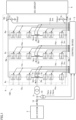
- Fig. 1 is a schematic configuration diagram of a power conversion device 100.
- the power conversion device 100 is connected between an alternating-current (AC) system 2 and a direct-current (DC) circuit 4, and is, for example, a power conversion device which is used for high-voltage DC power transmission.
- AC alternating-current
- DC direct-current
- the power conversion device 100 includes a voltage source power converter 6, which converts power between the AC system 2 and the DC circuit 4, and a control device 5.
- the power converter 6 is configured of a modular multilevel converter (MMC) power converter which includes multiple converter cells (corresponding to "CELL” in Fig. 1 ) 1 that are connected in series.
- MMC modular multilevel converter
- the "converter cell” will also be referred to as a "sub module” or "unit converter.”
- the power converter 6 includes multiple arms for each phase of the AC system 2. Specifically, the power converter 6 includes multiple leg circuits 8u, 8v, 8w (hereinafter, described as a "leg circuit 8" when referring to them collectively or referring to any of them) which are connected in parallel between a positive-side DC terminal (i.e., a high-potential-side DC terminal) Np and a negative-side DC terminal (i.e., a low-potential-side DC terminal) Nn.
- a positive-side DC terminal i.e., a high-potential-side DC terminal
- Nn negative-side DC terminal
- the leg circuit 8 is provided for each of the AC phases.
- the leg circuit 8 is connected between the AC system 2 and the DC circuit 4 and performs power conversion between the two.
- Fig. 1 shows the AC system 2 for three-phase AC current, which includes three leg circuits 8u, 8v, and 8w for u phase, v phase, and w phase, respectively. Note that if the AC system 2 is for a single-phase AC current, two leg circuits are provided.
- AC terminals Nu, Nv, and Nw which are respectively included in the leg circuits 8u, 8v, and 8w, are connected to the AC system 2 via a transformer 3.
- the AC system 2 is, for example, an AC power system, including an AC power supply, etc.
- Fig. 1 does not show the connections between the AC terminals Nv, Nw and the transformer 3.
- the DC terminals i.e., a positive-side DC terminal Np, a negative-side DC terminal Nn
- the DC circuit 4 is, for example, a DC power system, including a DC power grid and other power conversion device which performs DC output, etc.
- the leg circuits 8u, 8v, 8w may be connected to the AC system 2 via an interconnection reactor.
- the leg circuits 8u, 8v, 8w may include primary windings, instead of the AC terminals Nu, Nv, Nw, and the leg circuits 8u, 8v, 8w may be AC-coupled to the transformer 3 or the interconnection reactor via secondary windings that are magnetically coupled to the primary windings.
- the primary windings may be reactors 7a and 7b described below.
- leg circuit 8 is electrically (i.e., DC- or AC-) coupled to the AC system 2 via the connections such as the AC terminals Nu, Nv, Nw or the above-described primary windings, which are included in the leg circuits 8u, 8v, 8w.
- the leg circuit 8u is divided into a positive-side arm 13u extending from the positive-side DC terminal Np to the AC terminal Nu and a negative-side arm 14u extending from the negative-side DC terminal Nn to the AC terminal Nu.
- a point of connection between the positive-side arm 13u and the negative-side arm 14u is connected to the transformer 3, as the AC terminal Nu.
- the positive-side DC terminal Np and the negative-side DC terminal Nn are connected to the DC circuit 4.
- the leg circuit 8v includes a positive-side arm 13v and a negative-side arm 14v.
- the leg circuit 8w includes a positive-side arm 13w and a negative-side arm 14w.
- the leg circuits 8v, 8w have the same configuration as the leg circuit 8u. Thus, in the following, the leg circuit 8u will be representatively described.
- the positive-side arm 13u includes cascade-connected converter cells 1, and a reactor 7a.
- the converter cells 1 and the reactor 7a are connected in series.
- the negative-side arm 14u includes cascade-connected converter cells 1, and a reactor 7b.
- the converter cells 1 and the reactor 7b are connected in series.
- the reactor 7a may be inserted anywhere in the positive-side arm 13u.
- the reactor 7b may be insert anywhere in the negative-side arm 14u.
- the reactors may have different inductance values. Furthermore, only the reactor 7a of the positive-side arm 13u, or only the reactor 7b of the negative-side arm 14u may be provided.
- the power conversion device 100 further includes an AC voltage detector 10, an AC current detector 15, a DC voltage detectors 11a, 11b, and the arm current detectors 9a, 9b which are provided in the respective leg circuits 8. These detectors measure the electrical quantities (i.e., currents, voltages) which are used for the control of the power conversion device 100. Signals detected by the detectors are input to the control device 5.
- the AC voltage detector 10 detects a measured AC voltage value Vacu of the u phase of the AC system 2, a measured AC voltage value Vacv of the v phase, and a measured AC voltage value Vacw of the w phase.
- the AC current detectors 15 are each provided in the u phase, the v phase, and the w phase of the AC system 2, and detect a measured AC current value for each phase.
- the DC voltage detector 11a detects a measured DC voltage value Vdcp of the positive-side DC terminal Np connected to the DC circuit 4.
- the DC voltage detector 11b detects a measured DC voltage value Vdcn of the negative-side DC terminal Nn connected to the DC circuit 4.
- the arm current detectors 9a, 9b included in the leg circuit 8u for u phase detect a measured positive-side-arm current value Iup flowing through the positive-side arm 13u and a measured negative-side-arm current value Iun flowing through the negative-side arm 14u, respectively.
- the arm current detectors 9a, 9b included in the leg circuit 8v for v phase detect a measured positive-side-arm current value Ivp and a measured negative-side-arm current value Ivn, respectively.
- the arm current detectors 9a, 9b included in the leg circuit 8w for w phase detect a measured positive-side-arm current value Iwp and a measured negative-side-arm current value Iwn, respectively.
- a current flowing in a direction from the positive-side DC terminal Np to the negative-side DC terminal Nn is positive.
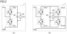
- Fig. 2 is a circuit diagram showing one example of the converter cell 1.
- the converter cell 1 shown in (a) of Fig. 2 has a circuit structure called a half-bridge configuration.
- the converter cell 1 includes a series body formed of two switching elements 31p, 31n being connected in series, a capacitor 32 as a power storage element, and a voltage detector 33.
- the series body and the capacitor 32 are connected in parallel.
- the voltage detector 33 detects a voltage Vc, which is a voltage across the capacitor 32.
- the converter cell 1 shown in (b) of Fig. 2 has a circuit structure called a full-bridge configuration.
- the converter cell 1 includes a first series body formed of two switching elements 31p1, 31n1 being connected in series, and a second series body formed of two switching elements 31p2, 31n2 being connected in series, a capacitor 32, and a voltage detector 33.
- the first series body, the second series body, and the capacitor 32 are connected in parallel.
- the voltage detector 33 detects the voltage Vc.
- the two switching elements 31p, 31n in (a) of Fig. 2 and the four switching elements 31p1, 31n1, 31p2, 31n2 in (b) of Fig. 2 are configured of, for example, a freewheeling diode being connected in anti-parallel to a self-turn-off semiconductor switching element such as an IGBT, a GCT thyristor, or a metal oxide semiconductor field-effect transistor (MOSFET).
- a capacitor such as a film capacitor is mainly used as the capacitor 32.
- switching elements 31p, 31n, 31p1, 31n1, 31p2, and 31n2 will also be collectively referred to as a switching element 31.
- the on/off of the semiconductor switching element included in the switching element 31 is also described simply as "on/off of the switching element 31.”
- the opposing terminals of the switching element 31n are referred to as input/output terminals P1 and P2.
- the voltage across the capacitor 32 and zero voltage are output by switching operations of the switching elements 31p and 31n. For example, when the switching element 31p is on and the switching element 31n is off, the voltage across the capacitor 32 is output. When the switching element 31p is off and the switching element 31n is on, zero voltage is output.
- the mid-point between the switching element 31p1 and the switching element 31n1, and the mid-point between the switching element 31p2 and the switching element 31n2 are the input/output terminals P1 and P2, respectively, of the converter cell 1.
- the converter cell 1 shown in (b) of Fig. 2 outputs a positive voltage or zero voltage by turning the switching element 31n2 on, the switching element 31p2 off, and alternately turning the switching elements 31p1 and 31n1 on.
- the converter cell 1 shown in (b) of Fig. 2 can output zero voltage or a negative voltage by turning the switching element 31n2 off, the switching element 31p2 on, and alternately turning the switching elements 31p1 and 31n1 on.
- the converter cell 1 may have the full-bridge configuration shown in (b) of Fig. 2 .
- any converter cell having a configuration other than those described above may be used, for example, a converter cell having a circuit structure, called a 1.5 half-bridge configuration applied thereto, in which the switching element 31p2 of (b) of Fig. 2 is replaced with a diode only.
- Fig. 3 is a block diagram showing one example hardware configuration of the control device 5.
- the control device 5 of Fig. 3 is configured based on a computer.
- the control device 5 includes one or more input converters 70, one or more sample and hold (S/H) circuits 71, a multiplexer (MUX) 72, and an analog-to-digital converter 73.
- the control device 5 further includes one or more central processing units (CPUs) 74, a random access memory (RAM) 75, and a read only memory (ROM) 76.
- the control device 5 further includes one or more input/output interfaces 77, an auxiliary storage 78, and a bus 79 interconnecting the above components.
- the input converter 70 includes an auxiliary transformer for each input channel.
- the auxiliary transformers each convert a detection signal by each electrical-quantity detector of Fig. 1 into a signal at a voltage level suitable for the subsequent signal processing.
- the sample and hold circuit 71 is provided for each input converter 70.
- the sample and hold circuit 71 samples and holds, at a predetermined sampling frequency, a signal representing the electrical quantity received from a corresponding input converter 70.
- the multiplexer 72 sequentially selects the signals held by the sample and hold circuits 71.
- the analog-to-digital converter 73 converts the signal, selected by the multiplexer 72, into a digital value. Note that the analog-to-digital conversions may be performed in parallel on the detection signals of multiple input channels by providing multiple analog-to-digital converters 73.
- the CPU 74 controls the entirety of the control device 5, and performs arithmetic operations according to programs.
- the RAM 75 as a volatile memory
- the ROM 76 as a non-volatile memory are used as primary storages of the CPU 74.
- the ROM 76 stores settings values for programs and signal processing, etc.
- the auxiliary storage 78 is a larger-capacity non-volatile memory, as compared to the ROM 76, and stores programs and data such as the electrical-quantity detection values.
- the input/output interface 77 is an interface circuit for communications between the CPU 74 and an external device.
- control device 5 may be configured using a field programmable gate array (FPGA) and an application specific integrated circuit (ASIC), etc.
- FPGA field programmable gate array
- ASIC application specific integrated circuit
- control device 5 may be configured of an analog circuit.
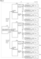
- Fig. 4 is a block diagram showing an overall configuration of the control device 5.
- Fig. 4 also shows respective converter cells 1.
- the control device 5 includes an arm-common controller 20, a u-phase arm controller 40u, a v-phase arm controller 40v, a w-phase arm controller 40w, and respective cell individual controllers 61.
- the configurations thereof are implemented by, for example, processing circuitry.
- the processing circuitry may be dedicated hardware or the CPU 74 for executing the programs stored in an internal memory of the control device 5. If the processing circuitry is dedicated hardware, the processing circuitry is configured of, for example, an FPGA, an ASIC, or a combination thereof.
- the arm-common controller 20 generates AC voltage command values Vacuref, Vacvref, and Vacwref for u phase, v phase, and w phase, based on measured arm-current values and measured AC voltage values.
- the arm-common controller 20 further outputs a DC voltage command value Vdcref.
- the arm-common controller 20 further generates an average capacitor voltage Vciav from measured capacitor voltage values Vci of the respective converter cells 1.
- the u-phase arm controller 40u generates a u-phase arm voltage command value, based on the AC voltage command value Vacuref and the DC voltage command value Vdcref received from the arm-common controller 20.
- the u-phase arm voltage command value includes a positive-side-arm voltage command value Vupref to be output to the positive-side arm 13u and a negative-side-arm voltage command value Vunref to be output to the negative-side arm 14u.
- the u-phase arm controller 40u further generates a circulating-voltage command value Vccuref based on an average capacitor-voltage value Vciav received from the arm-common controller 20 and a current u-phase circulating current.
- the circulating-voltage command value Vccuref is a voltage command value that is commonly output to the respective converter cells 1 of the positive-side arm 13u and the negative-side arm 14u to control the u-phase circulating current.
- the u-phase arm controller 40u further outputs an average positive-side-capacitor-voltage value Vcup to the respective cell individual controllers 61 of the positive-side arm 13u.
- the u-phase arm controller 40u also outputs an average negative-side-capacitor-voltage value Vcun to the respective cell individual controllers 61 of the negative-side arm 14u.
- the v-phase arm controller 40v generates a v-phase arm voltage command value, based on the AC voltage command value Vacvref and the DC voltage command value Vdcref.
- the v-phase arm voltage command value includes a positive-side-arm voltage command value Vvpref to be output to the positive-side arm 13v and a negative-side-arm voltage command value Vvnref to be output to the negative-side arm 14v.
- the v-phase arm controller 40v further generates a circulating-voltage command value Vccvref, based on the average capacitor-voltage value Vciav received from the arm-common controller 20 and a current v-phase circulating current.
- the circulating-voltage command value Vccvref is a voltage command value that is commonly output to the respective converter cells 1 of the positive-side arm 13v and the negative-side arm 14v to control the v-phase circulating current.
- the v-phase arm controller 40v further outputs an average positive-side-capacitor-voltage value Vcvp to the respective cell individual controllers 61 of the positive-side arm 13v.
- the v-phase arm controller 40v also outputs an average negative-side-capacitor-voltage value Vcvn to the respective cell individual controllers 61 of the negative-side arm 14v.
- the w-phase arm controller 40w generates a w-phase arm voltage command value, based on the AC voltage command value Vacwref and the DC voltage command value Vdcref.
- the w-phase arm voltage command value includes a positive-side-arm voltage command value Vwpref to be output to the positive-side arm 13w and a negative-side-arm voltage command value Vwnref to be output to the negative-side arm 14w.
- the w-phase arm controller 40w further generates a circulating-voltage command value Vccwref, based on the average capacitor-voltage value Vciav received from the arm-common controller 20 and a current w-phase circulating current.
- the circulating-voltage command value Vccwref is a voltage command value that is commonly output to the respective converter cells 1 of the positive-side arm 13w and the negative-side arm 14w to control the w-phase circulating current.
- the w-phase arm controller 40w further outputs an average positive-side-capacitor-voltage value Vcwp to the respective cell individual controllers 61 of the positive-side arm 13w.
- the w-phase arm controller 40w also outputs an average negative-side-capacitor-voltage value Vcwn to the respective cell individual controllers 61 of the negative-side arm 14w.
- the arm controllers 40u, 40v, 40w for each phase transmits the arm voltage command value, the circulating-voltage command value, and the average capacitor-voltage value to the cell individual controllers 61 for corresponding converter cells 1 via optical communication channels.
- Fig. 5 is a block diagram showing an operation of the arm-common controller 20.
- the arm-common controller 20 includes an AC control unit 35, a DC control unit 36, a current calculator 21, and an average-value calculator 22.
- the AC control unit 35 generates the AC voltage command values Vacuref, Vacvref, Vacwref, based on the measured AC voltage values Vacu, Vacv, Vacw detected by the AC voltage detector 10, the measured AC current value detected by the AC current detector 15, and AC current values Iacu, Iacv, Iacw calculated by the current calculator 21.
- the DC control unit 36 generates the DC voltage command value Vdcref.
- the DC control unit 36 has different configurations for a scenario where the power conversion device operates as a rectifier for supplying power from an AC circuit to a DC circuit and a scenario where the power conversion device operates as an inverter. If the power conversion device operates as a rectifier, the DC control unit 36 generates the DC voltage command value Vdcref based on the measured DC voltage values Vdcp, Vdcn.
- the DC control unit 36 If the power conversion device operates as an inverter, in contrast, the DC control unit 36 generates the DC voltage command value Vdcref, based on the measured AC voltage values Vacu, Vacv, Vacw, the measured AC current value for each phase detected by the AC current detector 15, and a DC current value Idc calculated by the current calculator 21.
- the AC current value Iacv and the leg current Icomv are calculated, using the measured positive-side-arm current value Ivp and the measured negative-side-arm current value Ivn, and, for the w phase, the AC current value Iacw and the leg current Icomw are calculated, using the measured positive-side-arm current value Iwp and the measured negative-side-arm current value Iwn, which are specifically represented by the following Equations (3) through (6):
- the positive-side DC terminals of the leg circuits 8u, 8v, 8w for the respective phases are commonly connected as the positive-side DC terminal Np, and the negative-side DC terminals are commonly connected as the negative-side DC terminal Nn.
- the current value obtained by adding up the leg currents Icomu, Icomv, Icomw of the respective phases, is the DC current value Idc that flows into the DC circuit 4 through the positive-side terminal of the DC circuit 4 and is fed back to the DC circuit 4 through the negative-side terminal of the DC circuit 4.
- the current capacity of the cells can be equalized.
- the difference between the leg currents and one-third of the DC current value can be calculated as a current value of the circulating current circulating through the power converter 6 (specifically, among the leg circuits 8 of the respective phases), without flowing through the DC circuit 4.
- Iccv Icomv ⁇ Idc / 3
- Iccw Icomw ⁇ Idc / 3
- the average-value calculator 22 calculates various average capacitor-voltage values Vciav from individual measured capacitor voltage values Vci detected at the respective converter cells 1.
- the average-value calculator 22 calculates an all-capacitor-voltage average value Vcall, which is an average voltage value of all the capacitors included in the entirety of the power converter 6.
- the average-value calculator 22 also calculates the average positive-side-capacitor-voltage value Vcup, which is an average voltage value of the respective capacitors included in the positive-side arm 13u, the average negative-side-capacitor-voltage value Vcun, which is an average voltage value of the respective capacitors included in the negative-side arm 14u, and the average capacitor-voltage value Vcu, which is an average voltage value of all the capacitors included in the entirety of the leg circuit 8u.
- the average-value calculator 22 calculates the average positive-side-capacitor-voltage value Vcvp at the positive-side arm 13v, the average negative-side-capacitor-voltage value Vcvn at the negative-side arm 14v, and the average capacitor-voltage value Vcv across the leg circuit 8v.
- the average-value calculator 22 calculates the average positive-side-capacitor-voltage value Vcwp at the positive-side arm 13w, the average negative-side-capacitor-voltage value Vcwn at the negative-side arm 14w, and the average capacitor-voltage value Vcw across the leg circuit 8w.
- the average capacitor-voltage value Vciav is a generic term for the above various average values.
- Fig. 6 is a diagram for illustrating an operation of the AC control unit 35 included in the arm-common controller 20.
- the AC control unit 35 includes an operator 23, a reactive-power controller 25, a reactive-current controller 27, a DC capacitor voltage controller 29, and an active-current controller 37.
- the AC control unit 35 further includes subtractors 24, 26, 28, 30, and a two-phase-to-three-phase converter 38.
- the operator 23 receives the measured AC voltage values Vacu, Vacv, Vacw of the respective phases, the measured AC current values of the respective phases of the AC system 2 detected by the AC current detector 15, and the AC current values Iacu, Iacv, Iacw calculated by the current calculator 21.
- the operator 23 calculates a reactive-power value Pr, based on the measured AC voltage values Vacu, Vacv, Vacw of the respective phases and the measured AC current values of the respective phases.
- the operator 23 further calculates an active-current value Ia and a reactive-current value Ir, based on the measured AC voltage values Vacu, Vacv, Vacw of the respective phases and the calculated AC current values Iacu, Iacv, Iacw.
- the subtractor 24 calculates a deviation ⁇ Pr between given reactive-power command value Prref and the reactive-power value Pr calculated by the operator 23.
- the reactive-power command value Prref may be a fixed value, or a variation that can be obtained by some calculation.
- the reactive-power controller 25 performs a feedback control for causing the reactive-power value Pr to follow the reactive-power command value Prref, thereby generating a reactive-current command value Irref, which is a command value for the reactive current output from the power converter 6.
- the reactive-power controller 25 performs a feedback operation for reducing the deviation ⁇ Pr less than a predetermined value (e.g., reducing the deviation ⁇ Pr to zero), thereby generating the reactive-current command value Irref.
- the subtractor 26 calculates a deviation ⁇ Ir between the reactive-current command value Irref and the reactive-current value Ir calculated by the operator 23.
- the reactive-current controller 27 performs a feedback control for causing the reactive-current value Ir to follow the reactive-current command value Irref, thereby generating a reactive-voltage command value Vrref, which is a command value for the reactive voltage output from the power converter 6.
- the reactive-current controller 27 performs a feedback operation for reducing the deviation ⁇ Ir less than a predetermined value (e.g., reducing the deviation ⁇ Ir to zero), thereby generating the reactive-current command value Irref.
- the subtractor 28 calculates a deviation ⁇ Vcall between a command value Vcallref given for the all-capacitor-voltage average value and the all-capacitor-voltage average value Vcall.
- the all-capacitor-voltage average value Vcall is obtained by averaging the measured capacitor voltage values Vci of the individual cells across the power conversion device.
- the command value Vcallref may be a fixed value, or a variation that can be obtained by some calculation.
- the DC capacitor voltage controller 29 performs a feedback control for causing the all-capacitor-voltage average value Vcall to follow the command value Vcallref, thereby generating an active-current command value Iaref, which is a command value for the active current output from the power converter 6.
- the DC capacitor voltage controller 29 performs a feedback operation for reducing the deviation ⁇ Vcall less than a predetermined value (e.g., reducing the deviation ⁇ Vcall to zero), thereby generating the active-current command value Iaref.
- the control by the DC capacitor voltage controller 29 corresponds to a total-voltage balance control in which the average voltage value (i.e., the all-capacitor-voltage average value Vcall) of all the capacitors included in the power converter 6 is caused to follow a command value.
- the average voltage value i.e., the all-capacitor-voltage average value Vcall
- the subtractor 30 calculates a deviation ⁇ Ia between the active-current command value Iaref and the active-current value Ia calculated by the operator 23.
- the active-current controller 37 performs a feedback control for causing the active-current value Ia to follow the active-current command value Iaref, thereby generating an active-voltage command value Varef, which is a command value for the active voltage output from the power converter 6.
- the active-current controller 37 performs a feedback operation for reducing the deviation ⁇ Ia less than a predetermined value (e.g., reducing the deviation ⁇ Ia to zero), thereby generating the active-voltage command value Varef.
- the reactive-power controller 25 may be configured as a PI controller which performs a proportional operation and an integration operation on the deviation ⁇ Pr, or may be configured as a PID controller which additionally performs a differential operation. Alternatively, a configuration of other controller used in a feedback control may be used as the reactive-power controller 25.
- the reactive-current controller 27, the DC capacitor voltage controller 29, and the active-current controller 37 each can be configured as a PI controller, a PID controller, or other controller that is used for the feedback control.
- the reactive-power controller 25 and the active-power controller 37 each may be a feedforward control or can be combined with a feedback controller.
- the two-phase-to-three-phase converter 38 generates the AC voltage command value Vacuref for u phase, the AC voltage command value Vacvref for v phase, and the AC voltage command value Vacwref for w phase through coordinate transformation from the active-voltage command value Varef and the reactive-voltage command value Vrref.
- the coordinate transformation by the two-phase-to-three-phase converter 38 can be implemented by, for example, an inverse Park transformation and an inverse Clarke transformation.
- the coordinate transformation by the two-phase-to-three-phase converter 38 can be implemented by an inverse Park transformation and a space vector transformation.
- Fig. 7 is a diagram for illustrating an operation of the DC control unit 36 in the arm-common controller 20.
- Part (a) of Fig. 7 shows a functional block diagram when the power conversion device 100 operates as a rectifier for supplying power from the AC system 2 to the DC circuit 4.
- Part (b) of Fig. 7 shows a functional block diagram when the power conversion device 100 operates as an inverter for supplying an active power from the DC circuit 4 to the AC system 2.
- the power conversion device 100 disposed at one end of a DC power transmission line includes the DC control unit 36 having the configuration of (a) of Fig. 7
- the power conversion device 100 disposed at the other end of the DC power transmission line includes the DC control unit 36 having the configuration of (b) of Fig. 7 .
- the DC control unit 36 for rectifier includes a subtractor 80 and a DC controller 81.
- the DC terminal voltage value Vdc is a sending-end voltage which is determined from the measured DC voltage values Vdcp, Vdcn detected by the DC voltage detectors 11a, 11b.
- the DC controller 81 performs a feedback control for causing the DC terminal voltage value Vdc to follow the DC terminal voltage command value, thereby generating the DC voltage command value Vdcref, which is a command value for the DC voltage output from the power converter 6.
- the DC controller 81 performs a feedback operation for reducing the deviation ⁇ Vdc less than a predetermined value (e.g., reducing the deviation ⁇ Vdc to zero), thereby generating the DC voltage command value Vdcref.
- the DC control unit 36 for inverter includes an operator 82, subtractors 83, 85, an active-power controller 84, and a DC current controller 86.
- the operator 82 receives the measured AC voltage values Vacu, Vacv, Vacw of the respective phases, and the measured AC current values of the respective phases of the AC system 2 detected by the AC current detector 15.
- the operator 82 calculates an active-power value Pa, based on these voltage values and current values.
- the subtractor 83 calculates a deviation ⁇ Pa between a given active-power command value Paref and the calculated active-power value Pa.
- the active-power command value Paref may be a fixed value, or a variation that can be obtained by some calculation.
- the active-power controller 84 performs a feedback control for causing the active-power value Pa to follow the active-power command value Paref, thereby generating a DC-current command value Idcref, which is a command value for the DC current output from the power converter 6.
- the active-power controller 84 performs a feedback operation for reducing the deviation ⁇ Pa less than a predetermined value (e.g., reducing the deviation ⁇ Pa to zero), thereby generating the DC-current command value Idcref.
- the subtractor 85 calculates a deviation ⁇ Idc between the DC-current command value Idcref and the DC current value Idc.
- the DC current value Idc is calculated by the current calculator 21, using the respective measured arm-current values. Note that the DC current value Idc may be directly detected by using the DC current detector.
- the DC current controller 86 performs a feedback control for causing the DC current value Idc to follow the DC-current command value Idcref, thereby generating the DC voltage command value Vdcref, which is a command value for the DC voltage output from the power converter 6.
- the DC current controller 86 performs a feedback operation for reducing the deviation ⁇ Idc less than a predetermined value (e.g., reducing the deviation ⁇ Idc to zero), thereby generating the DC voltage command value Vdcref.
- the DC controller 81, the active-power controller 84, and the DC current controller 86 each can be configured as a PI controller, a PID controller, or other controller that is used for the feedback control.
- Fig. 8 is a block diagram showing an operation of the u-phase arm controller 40u.
- the u-phase arm controller 40u includes a positive-side command generator 41, a negative-side command generator 42, an inter-group balance control unit 55, and a circulating-current controller 51.
- the u-phase arm controller 40u further includes adders 45, 46, 53 and subtractors 48, 49, 50.
- the adder 45 adds up the DC voltage command value Vdcref and a value obtained by the positive-side command generator 41 multiplying the AC voltage command value Vacuref by -1. This generates the positive-side-arm voltage command value Vupref for u phase.
- the adder 46 adds up the DC voltage command value Vdcref and a value obtained by the negative-side command generator 42 multiplying the AC voltage command value Vacuref by +1. This generates the negative-side-arm voltage command value Vunref for u phase.
- the oscillation control unit 57 Based on the measured capacitor voltage values Vci of the respective converter cells 1, the oscillation control unit 57 outputs an oscillating component Vf for causing an inter-phase balance voltage command value Vxuref to oscillate. In order to correct the imbalance between the capacitor voltages of the respective converter cells 1 within an arm, the oscillating component Vf is superimposed onto the inter-phase balance voltage command value Vxuref, depending on a condition described below. Details of the oscillation control unit 57 will be described below.
- the adder 53 adds up the oscillating component Vf and the inter-phase balance voltage command value Vxuref. This generates an inter-phase balance voltage command value Vxuref* in which the oscillating component Vf is superimposed on the inter-phase balance voltage command value Vxuref.
- the inter-phase balance voltage command value Vxuref is the all-capacitor-voltage average value Vcall.
- the subtractor 48 calculates a deviation ⁇ Vcu between the inter-phase balance voltage command value Vxuref* and the average capacitor-voltage value Vcu of the u phase.
- the deviation ⁇ Vcu refers to variations in voltage of capacitors (i.e., variations in capacitor voltage) between different phases.
- the subtractor 49 calculates a deviation ⁇ Vcupn between a positive/negative balance voltage command value Vyuref and the average negative-side-capacitor-voltage value Vcun of the u phase.
- the positive/negative balance voltage command value Vyuref is the average positive-side-capacitor-voltage value Vcup.
- the deviation ⁇ Vcupn refers to variations in voltage of capacitors between the positive-side arm 13u and the negative-side arm 14u.
- the inter-group balance control unit 55 controls the balance of the voltages of the capacitors 32 between predetermined groups (e.g., between the phases or between the arms), based on a balance command value (e.g., the inter-phase balance voltage command value Vxuref or the positive/negative balance voltage command value Vyuref). Specifically, the inter-group balance control unit 55 generates a circulating-current command value Iccuref for balancing the voltages of the capacitors 32 between the predetermined groups, based on the balance command value. Specifically, the inter-group balance control unit 55 includes an inter-phase balance controller 43, a positive-negative balance controller 44, and an adder 47.
- a balance command value e.g., the inter-phase balance voltage command value Vxuref or the positive/negative balance voltage command value Vyuref.
- the inter-phase balance controller 43 performs a feedback control for causing the average voltage value of the respective capacitors 32 included in the leg circuit 8u (i.e., the average capacitor-voltage value Vcu) to follow the inter-phase balance voltage command value Vxuref*, thereby controlling the balance of the voltages of the capacitors 32 between phases. Specifically, the inter-phase balance controller 43 performs a feedback operation for reducing the deviation ⁇ Vcu less than a predetermined value (e.g., reducing the deviation ⁇ Vcu to zero).
- a predetermined value e.g., reducing the deviation ⁇ Vcu to zero.
- the control by the inter-phase balance controller 43 corresponds to an inter-phase balancing voltage control for causing the average voltage value of all the capacitors included in a phase (e.g., the u phase) (e.g., the average capacitor-voltage value Vcu of the u phase) to match the command value.
- a phase e.g., the u phase
- Vcu of the u phase the average capacitor-voltage value
- the positive-negative balance controller 44 performs a feedback control for causing the average negative-side-capacitor-voltage value Vcun to follow the positive/negative balance voltage command value Vyuref (i.e., the average positive-side-capacitor-voltage value Vcup), thereby controlling the balance of the voltages of the capacitors 32 between the positive-side and negative-side arms. Specifically, the positive-negative balance controller 44 performs a feedback operation for reducing the deviation ⁇ Vcupn less than a predetermined value (e.g., reducing the deviation ⁇ Vcupn to zero).
- a predetermined value e.g., reducing the deviation ⁇ Vcupn to zero.
- the positive-negative balance controller 44 performs a feedback control for causing the average positive-side-capacitor-voltage value Vcup to follow the average negative-side-capacitor-voltage value Vcun.
- the control by the positive-negative balance controller 44 corresponds to a balancing voltage control between the positive-side and negative-side arms for causing the average voltage value of all the capacitors (e.g., the average negative-side-capacitor-voltage value Vcun) included in one arm (e.g., the negative-side arm) of a phase (e.g., the u phase) to match the command value (e.g., the average positive-side-capacitor-voltage value Vcup).
- the average voltage value of all the capacitors e.g., the average negative-side-capacitor-voltage value Vcun
- the subtractor 50 calculates the deviation between the circulating-current command value Iccuref and the circulating current Iccu.
- the circulating-current controller 51 controls the circulating current Iccu, based on the circulating-current command value Iccuref. Specifically, the circulating-current controller 51 performs an operation on the deviation calculated by the subtractor 50 to generate the circulating-voltage command value Vccuref of the u phase for controlling the circulating current Iccu.
- the positive-side-arm voltage command value Vupref, the circulating-voltage command value Vccuref, and the average positive-side-capacitor-voltage value Vcup are transmitted to the cell individual controllers 61 of the respective converter cells 1 included in the positive-side arm 13u. Furthermore, the negative-side-arm voltage command value Vunref, the circulating-voltage command value Vccuref, and the average negative-side-capacitor-voltage value Vcun are transmitted to the cell individual controllers 61 of the respective converter cells 1 included in the negative-side arm 14u.
- inter-phase balance controller 43 the positive-negative balance controller 44, and the circulating-current controller 51 each can be configured as, for example, a PI controller, a PID controller, or other controller that is used for the feedback control.
- the average voltage value of the respective capacitors is used as the voltage representative of the capacitors
- the average negative-side-capacitor-voltage value Vcun is used as the voltage representative of the respective capacitors included in the negative-side arm 14u
- the average positive-side-capacitor-voltage value Vcup is used as the voltage representative of the respective capacitors included in the positive-side arm 13u.
- the average voltage value is used as the voltage representative.
- the present disclosure is not limited thereto.
- the voltage representative may be the maximum voltage value, the minimum voltage value, or a median voltage of the respective capacitors, or the voltage value of the capacitor of a representative converter cell.
- An operation of the cell individual controller 61 provided for each converter cell 1 is now described.
- an operation of a cell individual controller 61 for the positive-side arm 13u will be representatively described.
- An operation of a cell individual controller 61 for the negative-side arm 14u is the same as the operation of the cell individual controller 61 for the positive-side arm 13u with the positive side in the following description being replaced by the negative side.
- An operation of the cell individual controller 61 for the v phase or the w phase are the same as the operation of the cell individual controller 61 for the positive-side arm 13u with the u phase in the following description being replaced by the v phase or the w phase.
- Fig. 9 is a block diagram showing an operation of a cell individual controller 61 for the positive-side arm 13u.
- an analog-to-digital converter for converting the measured capacitor voltage value Vci into a digital value is not shown.
- the cell individual controller 61 includes a capacitor voltage controller 64, a carrier generator 65, a comparator 67, a subtractor 63, and an adder 66.
- the subtractor 63 calculates the deviation ⁇ Vcup between the average positive-side-capacitor-voltage value Vcup as the capacitor voltage command value and the measured capacitor voltage value Vci. As described with respect to Fig. 8 , the average positive-side-capacitor-voltage value Vcup is received from the corresponding u-phase arm controller 40u. The measured capacitor voltage value Vci is detected at a corresponding converter cell 1.
- the capacitor voltage controller 64 performs a feedback control for causing the measured capacitor voltage value Vci to follow the average positive-side-capacitor-voltage value Vcup.
- the capacitor voltage controller 64 performs a feedback operation for reducing the deviation ⁇ Vcup less than a predetermined value (e.g., reducing the deviation ⁇ Vcup to zero).
- the control by the capacitor voltage controller 64 corresponds to an individual balancing voltage control for causing the voltages of the respective capacitors 32 included in one arm (e.g., the positive-side arm) of a phase (e.g., the u phase) to match the command value (e.g., the average voltage value of the respective capacitors).
- the capacitor voltage controller 64 can be configured as, for example, a proportional controller, a PI controller, a PID controller, or other controller that is used for the feedback control.
- the individual balancing voltage control changes the voltages output from the respective converter cells, thereby controlling the distribution of the energy flowing in and out of the arms to the respective converter cells to control the balance of the voltages between the respective converter cells.
- the individual balancing voltage control due to its properties, has a reduced effect with a reduced energy flowing in and out of the arms.
- the adder 66 adds up the positive-side-arm voltage command value Vupref of the u phase and the output of the capacitor voltage controller 64 to generate a final positive-side-arm voltage command value Vupref* for the u phase.
- the carrier generator 65 generates a carrier signal CS, which is used for a phase-shift pulse width modulation (PWM) control.
- the phase-shift PWM control shifts the timing at which the PWM signal is output to the respective converter cells 1 included in the positive-side arm 13u. This can reduce the harmonics components included in the combined voltage of the output voltages of the respective converter cells 1.
- the cell individual controllers 61 included in the respective converter cells 1 generate the carrier signals CS whose phases are shifted to each other. For example, a triangular wave is used as the carrier signal CS.
- the carrier generator 65 modulates the generated carrier signal CS in accordance with the circulating-voltage command value Vccuref.
- the carrier generator 65 then, outputs the modulated carrier signal to the downstream comparator 67.
- the PWM signals i.e., gate control signals Ga, Gb
- the PWM signals generated by the downstream comparator 67 change in pulse width, responsive to the circulating-voltage command value Vccuref.
- the deviation between the circulating-current command value Iccuref and the circulating current Iccu is controlled to be even smaller.
- the comparator 67 compares the positive-side-arm voltage command value Vupref* and the modulated carrier signal CS based on the circulating-voltage command value Vccuref. According to a result of the comparison, the comparator 67 generates the gate control signals Ga, Gb as PWM-modulated signals for controlling the switching elements 31p, 31n included in the converter cell 1.
- the gate control signals Ga, Gb are supplied to the control electrodes of the switching elements 31p, 31n, respectively, of Fig. 2 .
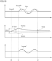
- Fig. 10 is a diagram showing a relationship between the inter-phase balance voltage command value, the capacitor voltage of the converter cell, and the circulating-current command value.
- the voltages of the respective capacitors 32 i.e., the capacitor voltages
- the u-phase arm e.g., the positive-side arm 13u or the negative-side arm 14u
- the oscillation control unit 57 of Fig. 8 always monitors the difference ⁇ Vcai, based on the voltages of the respective capacitors 32 included in the u-phase arm.
- the oscillation control unit 57 outputs the oscillating component Vf.
- the oscillating component Vf is an oscillating voltage which has a frequency f1 lower than a fundamental frequency Fs (e.g., 60 Hz) of the AC system 2.
- the frequency f1 is set to an integer fraction (e.g., 1/6) of the fundamental frequency Fs. Due to this, the adder 53 of Fig. 8 generates the inter-phase balance voltage command value Vxuref* by adding up the inter-phase balance voltage command value Vxuref and the oscillating component Vf.
- the frequency f1 is not limited to be set to an integer fraction of the fundamental frequency Fs, and may be set, considering the harmonics characteristics on the AC system 2 side, to any frequency that can minimize the effects of the AC system 2.
- the inter-phase balance voltage command value Vxuref* periodically oscillates due to having the oscillating component Vf having the frequency f1 superimposed thereon.
- the average capacitor-voltage value Vcu of the u phase follows the inter-phase balance voltage command value Vxuref*.
- the periodic oscillation of the inter-phase balance voltage command value Vxuref* causes the circulating-current command value Iccuref of the u phase, output from the inter-group balance control unit 55, to vary.
- the circulating-current controller 51 of Fig. 8 performs the feedback control to cause the circulating current Iccu to follow the circulating-current command value Iccuref, thereby generating the circulating-voltage command value Vccuref.
- the cell individual controller 61 of the respective converter cell 1 operates in accordance with the circulating-voltage command value Vccuref. This causes the circulating current Iccu, following the circulating-current command value Iccuref varying as illustrated in Fig. 10 , to flow into the power converter 6 (i.e., the circulating current Iccu to increase), allowing the individual balancing voltage control by the cell individual controller 61 (specifically, the capacitor voltage controller 64) of the respective converter cell 1 to start effectively function. This gradually reduces the difference ⁇ Vcai at and after time t1.
- the oscillation control unit 57 stops the output of the oscillating component Vf. This causes the adder 53 to output the inter-phase balance voltage command value Vxuref, as is, to the inter-phase balance controller 43. Since the inter-phase balance voltage command value Vxuref does not oscillate, the oscillation of the circulating-current command value Iccuref stops. Note that a hysteresis, where Vth1 > Vth2, is provided to prevent frequent switching (what is called, chattering) between start and stop of the oscillating control.
- the oscillation control unit 57 causes the inter-phase balance voltage command value Vxuref to oscillate at the frequency f1 less than the fundamental frequency Fs. Specifically, the oscillation control unit 57 extracts the maximum voltage value Vcmax and the minimum voltage value Vcmin from among the measured capacitor voltage values Vci of the respective capacitors 32 included in the arm. The oscillation control unit 57 calculates the difference ⁇ Vcai between the maximum voltage value Vcmax and the minimum voltage value Vcmin, and performs the oscillating control that superimposes the oscillating component Vf having the frequency f1 onto the inter-phase balance voltage command value Vxuref, based on the difference ⁇ Vcai.
- the oscillation control unit 57 starts the oscillating control (i.e., outputs the oscillating component Vf). After starting the oscillating control, the oscillation control unit 57 stops the oscillating control (i.e., stops the output of the oscillating component Vf) if the difference ⁇ Vcai decreases less than or equal to the threshold Vth2.
- Fig. 11 is a diagram illustrating one example of changes over time in maximum value and minimum value of the capacitor voltages. Specifically, (a) of Fig. 11 illustrates the changes over time when the AC current output of the power converter 6 is large. Part (b) of Fig. 11 illustrates the changes over time when the AC current output of the power converter 6 is small.
- a graph 210 illustrates changes over time in the maximum voltage value Vcmax among the respective capacitors 32 included in the u-phase arm (e.g., the positive-side arm 13u or the negative-side arm 14u).
- a graph 220 illustrates changes over time in the minimum voltage value Vcmin of the respective capacitors 32.
- a graph 230 illustrates changes over time in a minimum value min_max among the maximum voltage values Vcmax during a period of time.
- a graph 240 illustrates changes over time in a maximum value Vmax_min among the minimum voltage values Vcmin during a period of time.
- the minimum value Vmin_max among the maximum voltage values Vcmax during the period of time, is a value obtained by suppressing the rates of change in the directions of increases of the respective maximum voltage values Vcmax.
- the maximum value Vmax_min among the minimum voltage values Vcmin during the period of time, is a value obtained by suppressing the rates of change in the directions of decreases of the respective minimum voltage values Vcmin.
- the minimum value Vmin_max among the maximum voltage values Vcmax per period of the AC system 2, is generally constant, as illustrated in the graph 230. This is because the rate of change of the minimum value Vmin_max in the direction of increase (i.e., the positive direction) is restricted by applying a rate-of-change suppressing limiter to the minimum value Vmin_max.
- the maximum value Vmax_min among the minimum voltage values Vcmin, is generally constant, as illustrated in the graph 240. This is because the rate of change of the maximum value Vmax_min in the direction of decrease (i.e., the negative direction) is restricted by applying a rate-of-change suppressing limiter to the maximum value Vmax_min.
- the oscillation control unit 57 performs an oscillating control that superimposes the oscillating component Vf having the frequency f1 onto the inter-phase balance voltage command value Vxuref, based on a difference ⁇ Vaix between the minimum value Vmin_max and the maximum value Vmax_min.
- the oscillation control unit 57 starts the oscillating control (i.e., outputs the oscillating component Vf). Therefore, if the maximum value Vmax_min is greater than the minimum value Vmin_max as in the example of (a) of Fig. 11 , the difference ⁇ Vaix is a negative value, and the oscillating control is, thus, not started. This is because the capacitor voltages are balanced when the difference ⁇ Vaix is a negative value.
- the maximum voltage value Vcmax and the minimum voltage value Vcmin have little oscillating component, as illustrated in the graphs 210 and 220. Accordingly, the minimum value Vmin_max illustrated in the graph 230 substantially matches the maximum voltage value Vcmax illustrated in the graph 210, and the maximum value Vmax_min illustrated in the graph 240 substantially matches the minimum voltage value Vcmin illustrated in the graph 220.
- the rates of change of the minimum value Vmin_max and the maximum value Vmax_min are controlled by applying the rate-of-change suppressing limiters to the minimum value Vmin_max and the maximum value Vmax_min.
- an alternative operation method such as maintaining the minimum value Vmin_max and the maximum value Vmax_min at the previous values may be employed, instead of the rate-of-change suppressing limiters, if the method can compare the minimum value of the capacitor maximum voltage values during a period of time and the maximum value of the capacitor minimum voltage values during a period of time.
- the oscillation control unit 57 detects, during one period, a maximum voltage value Vcmax that is less than the current minimum value Vmin_max of the maximum voltage values Vcmax, the oscillation control unit 57 updates the minimum value Vmin_max, using the maximum voltage value Vcmax as a new minimum value Vmin_max. If the oscillation control unit 57 detects no maximum voltage value Vcmax less than the current minimum value Vmin_max, the oscillation control unit 57 maintains the current minimum value Vmin_max.
- the oscillation control unit 57 detects, during one period, a minimum voltage value Vcmin that is greater than the current maximum value Vmax_min of the minimum voltage values Vcmin, the oscillation control unit 57 updates the maximum value Vmax_min, using the minimum voltage value Vcmin as a new maximum value Vmax_min. If the oscillation control unit 57 detects no minimum voltage value Vcmin greater than the current maximum value Vmax_min, the oscillation control unit 57 maintains the current maximum value Vmax_min.
- the oscillation control unit 57 starts the oscillating control. If the difference ⁇ Vaix decreases less than or equal to the threshold Vth4 (provided that Vth4 > 0) less than the threshold Vth3, the oscillation control unit 57 stops the oscillating control.
- the oscillation control unit 57 performs the oscillating control, based on the difference ⁇ Vaix between the minimum value Vmin_max and the maximum value Vmax_min during one period, thereby determining whether to start or stop the oscillating control, taking into an account the effects of the ripple component.
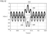
- Fig. 12 is a diagram showing another example of changes over time in maximum value and minimum value of the capacitor voltages.
- a graph 310 illustrates changes over time in the maximum voltage value Vcmax of the respective capacitors 32 included in the u-phase arm.
- a graph 320 illustrates changes over time in the minimum voltage value Vcmin of the respective capacitors 32.
- a graph 330 illustrates changes over time in the minimum value Vmin_max among the maximum voltage values Vcmax during a period of time.
- a graph 340 illustrates changes over time in the maximum value Vmax_min among the minimum voltage values Vcmin during a period of time.
- the maximum voltage value Vcmax suddenly increases and the minimum voltage value Vcmin suddenly decreases around 0.1s to 0.15s, causing the capacitor voltages to be imbalanced. It can be understood that at and after 0.15s, however, the maximum voltage value Vcmax and the minimum voltage value Vcmin return to the steady state (i.e., the capacitor voltages return to be balanced).
- the minimum value Vmin_max of the maximum voltage values Vcmax during one period of the AC system 2 is generally constant. This is because the minimum value Vmin_max is restricted from changing in the direction of increase, by applying the rate-of-change suppressing limiter to the minimum value Vmin_max.
- the maximum value Vmax_min of the minimum voltage values Vcmin is generally constant too. This is because the maximum value Vmax_min is restricted from changing in the direction of decrease, by applying the rate-of-change suppressing limiter to the maximum value Vmax_min.
- the oscillation control unit 57 performs the oscillating control that superimposes the oscillating component Vf having the frequency f1 onto the inter-phase balance voltage command value Vxuref, based on the difference ⁇ Vaix between the minimum value Vmin_max and the maximum value Vmax_min. Because of this, the oscillating control does not start in response to the transitional imbalance in capacitor voltages around 0.1s to 0.15s. Accordingly, the oscillation control unit 57 is able to perform the oscillating control at more appropriate timing.
- the oscillation control unit 57 may determine whether to start or stop the oscillating control, focusing on the oscillation of the average capacitor-voltage value.
- the oscillation control unit 57 starts the oscillating control that superimposes the oscillating component Vf having the frequency f1 onto the inter-phase balance voltage command value Vxuref. If the amplitude of the fundamental frequency component increases greater than or equal to a threshold Vth6 greater than the threshold Vth5, the oscillation control unit 57 stops the oscillating control.
- the oscillation control unit 57 may intermittently perform the oscillating control. For example, if the amplitude of the above fundamental frequency component is less than or equal to the threshold Vth5, the oscillation control unit 57 may perform the oscillating control so as to repeatedly alternate between superimposing the oscillating component Vf onto the inter-phase balance voltage command value Vxuref and not superimposing the oscillating component Vf onto the inter-phase balance voltage command value Vxuref. In this case, the oscillation control unit 57 intermittently outputs the oscillating component Vf to the adder 53.
- the control device 5 when the capacitor voltages within an arm become imbalanced, the control device 5 superimposes the oscillating component onto the inter-phase balance voltage command value to cause the circulating-current command value to oscillate, causing the circulating current to flow through the phase. This can cause the individual balancing voltage control to efficiently function.
- the control device 5 performs the oscillating control that causes the inter-phase balance voltage command value, which is used for the balance control over the capacitor voltages between phases, to oscillate depending on the balance of the capacitors 32 within the arm, and when the variations (e.g., ⁇ Vcai) in voltage of the capacitors 32 within the arm fall within a set range (e.g., when ⁇ Vcai ⁇ Vth2 stands true), the control device 5 stops the oscillating control. This causes the control device 5 to stop the oscillating control before the capacitors 32 in the same arm provide the same voltage. This is because in the individual balancing voltage control, the variations in capacitor voltage within the same arm (e.g., ⁇ Vcai) may be kept within a certain margin, and there is, therefore, no need for the respective converter cells 1 to provide the same capacitor voltage.
- the variations in capacitor voltage within the same arm e.g., ⁇ Vcai
- the frequency f1 of the oscillating component Vf is set lower than the fundamental frequency Fs. Therefore, the control is not required to be at high speed. Moreover, typically, the frequency that is an integer multiple of the fundamental frequency of the AC system 2 is important in evaluating the outflow of the harmonics into the AC system 2. Thus, the outflow of an integer-multiple harmonics into the AC system 2 should be reduced.
- the circulating current having an integer-multiple frequency, flowing into the power converter 6, may be a cause of the outflow of the integer-multiple harmonics into the AC system 2, and is, therefore, desirably, be suppressed.
- the outflow of the integer-multiple harmonics to the AC system 2 side can be suppressed, and, moreover, even in the event of outflow of the integer-multiple harmonics, the impact on other devices can be suppressed.
- an arm voltage e.g., the u-phase arm voltage
- a circulating current e.g., the u-phase circulating current
- an arm power (hereinafter, also referred to simply as an "arm power") associated with the flow of the circulating current, which is calculated by multiplying the arm voltage by the circulating current, are now considered, where the oscillating component Vf having the frequency f1 of various values is superimposed onto the inter-phase balance voltage command value Vxuref.
- Fig. 13 is a diagram illustrating one example of changes over time in arm voltage, circulating current, and arm power. Specifically, (a) of Fig. 13 illustrates changes over time in arm voltage and circulating current when the frequency f1 is set 0.15 times the fundamental frequency Fs. Part (b) of Fig. 13 illustrates changes over time in arm power and arm integral power when the frequency f1 is set 0.15 times the fundamental frequency Fs.
- a graph 410 illustrates changes in arm voltage over time.
- a graph 420 illustrates changes in circulating current over time. Setting the frequency f1 0.15 times the fundamental frequency Fs results in the frequency of the circulating current being 0.15 times the frequency of the arm voltage.
- Time Ta corresponds to one period of the arm voltage.
- a graph 430 illustrates changes in arm power over time.
- a graph 440 illustrates changes in arm integral power over time.
- One period of the arm power is the time period Ta, which is the same as one period of the arm voltage.
- the arm integral power is not zero at a time instance after the elapse of the time period Ta since time ts (i.e., after the elapse of one period of the arm power). Continuously, the arm integral power does not go to zero each time the time period Ta elapses. This means that the time average value of one period of the arm power does not go to zero. As such, if the frequency f1 is set lower than the fundamental frequency Fs, the time average value of one period of the arm power does not go to zero.
- Fig. 14 is a diagram showing another example of changes over time in arm voltage, circulating current, and arm power. Specifically, (a) of Fig. 14 shows changes over time in arm voltage and circulating current when the frequency f1 is set double the fundamental frequency Fs. Part (b) of Fig. 14 shows changes over time in arm power and arm integral power when the frequency f1 is set double the fundamental frequency Fs.
- a graph 510 illustrates changes in arm voltage over time
- a graph 520 illustrates changes in circulating current over time. Setting the frequency f1 double the fundamental frequency Fs results in the frequency of the circulating current being double the frequency of the arm voltage.
- the time period Tb corresponds to one period of the arm voltage.
- a graph 530 illustrates changes in arm power over time
- a graph 540 illustrates changes in arm integral power over time.
- One period of the arm power is the time period Tb, which is the same as one period of the arm voltage.
- the arm integral power is zero at a time instance after the elapse of the time period Tb since time ts. Continuously, the arm integral power goes to zero each time the time period Tb elapses. This means that the time average value of one period of the arm power goes to zero.
- the frequency f1 is set double the fundamental frequency Fs
- the time average value of one period of the arm power go to zero. Note that if the frequency f1 is set to an integer multiple equal to greater than twice the fundamental frequency Fs, the time average value of one period of the arm power goes to zero.
- Fig. 15 is a diagram showing still another example of changes over time in arm voltage, circulating current, and arm power. Specifically, (a) of Fig. 15 shows changes over time in arm voltage and circulating current when the frequency f1 is set identical to the fundamental frequency Fs and the phase of the oscillating component Vf is shifted by 90 degrees from the phase of the AC system 2. Part (b) of Fig. 15 shows changes over time in arm power and arm integral power when the frequency f1 is set identical to the fundamental frequency Fs and the phase of the oscillating component Vf is shifted by 90 degrees from the phase of the AC system 2.
- a graph 610 illustrates changes in arm voltage over time
- a graph 620 illustrates changes in circulating current over time.
- Setting the frequency f1 identical to the fundamental frequency Fs results in the frequency of the circulating current being identical to the frequency of the arm voltage.
- the phase of the oscillating component Vf being shifted by 90 degrees from the phase of the AC system 2 results in the phase of the circulating current being shifted by 90 degrees from the phase of the arm voltage.
- a time period Tc corresponds to one period of the arm voltage.
- a graph 630 illustrates changes in arm power over time
- a graph 640 illustrates changes in arm integral power over time
- a time period Td corresponds to one period of the arm power.
- the arm integral power is zero at a time instance after the elapse of the time period Td since time ts. Continuously, the arm integral power goes to zero each time the time period Td elapses. This means that the time average value of one period of the arm power goes to zero.
- the frequency f1 is set identical to the fundamental frequency Fs and the phase of the oscillating component Vf is shifted by 90 degrees from the phase of the AC system 2, the time average value of one period of the arm power goes to zero.
- the time average value of one period of the arm power is not zero when the frequency f1 is lower than the fundamental frequency Fs.
- the time average value of one period of the arm power is zero when the frequency f1 is an integer multiple of the fundamental frequency Fs, or when the frequency f1 is identical to the fundamental frequency Fs and the phase of the oscillating component Vf is shifted by 90 degrees from the phase of the AC system 2.
- the frequency f1 is lower than the fundamental frequency Fs, the time average value of one period of the arm power, therefore, does not go to zero.
Landscapes
- Engineering & Computer Science (AREA)
- Power Engineering (AREA)
- Inverter Devices (AREA)
Abstract
Description
- The present disclosure relates to a power conversion device.
- As a large-capacity power conversion device installed in a power system, a modular multilevel converter (MMC) is known in which multiple unit converters (hereinafter, also referred to as "converter cells") are cascade-connected. The converter cell includes multiple switching elements and a power storage element (e.g., a capacitor).
- In the modular multilevel converter, in order to obtain a desired control output, it is necessary to maintain the voltages (hereinafter, also referred to as "capacitor voltages") of the power storage elements of individual converter cells close to a target value. If the capacitor voltages deviate from the target value, the output voltages of the converter cells are not as directed, causing a concern that the control characteristics may be deteriorated by generation of an unintended circulating current, etc. If this is significant, the capacitor voltage in any of the converter cells may excessively increase to a level of overvoltage protection or excessively decrease to a level of low-voltage protection level, and the operation of the MMC may thereby stop.
- Typically, the capacitor voltages are controlled in multiple levels by the balance control of the converter cells as a whole within the MMC, and the balance control between certain groups (e.g., arms or phases), in addition of the balance control for each of individual converter cells.
- The power conversion device according to
Japanese Patent Laying-Open No. 2016-123159 - The power conversion device according to
Japanese Patent Laying-Open No. 2019-30106 -
- PTL 1:
Japanese Patent Laying-Open No. 2016-123159 - PTL 2:
Japanese Patent Laying-Open No. 2019-30106 -
PTL 1 considers keeping the capacitor voltages at the rated value and reducing the current distortion of a converter while the load operation is stopped.PTL 2 considers, when the AC power is less than a reference value, causing, by the second circulating-current command value, the individual balance controls to function and setting the second circulating-current command value so that the time average value of the power is zero, thereby preventing the average capacitor-voltage value from varying. However, if, for example, the harmonics component of the system voltage increases, the capacitor voltages may lose the balance even while the current output to the load is not ceased or even if the AC power is greater than or equal to the reference value. - An object of a certain aspect of the present disclosure is to provide a power conversion device which can stably control the capacitor voltages of the converter cells.
- According to a certain embodiment, a power conversion device connected to an AC system is provided. The power conversion device includes: a power converter which includes a plurality of arms for each phase of the alternating-current system; and a control device to control the power converter. Each arm, among the plurality of arms, has a plurality of converter cells that are cascade-connected. The plurality of converter cells each have a plurality of switching elements, and a power storage element connected to the plurality of switching elements. The control device includes: a balance control unit to control a balance of voltages of power storage elements between predetermined groups, based on a balance command value; a circulating-current control unit to control a circulating current circulating through the power converter, based on a circulating-current command value; and an oscillation control unit to cause the balance command value to oscillate at a first frequency lower than a fundamental frequency of the alternating-current system, based on the voltages of the power storage elements included in the arm.
- According to other embodiment, a power conversion device connected to an AC system is provided. The power conversion device includes: a power converter which includes a plurality of arms for each phase of the alternating-current system; and a control device to control the power converter. Each arm, among the plurality of arms, has a plurality of converter cells that are cascade-connected. The plurality of converter cells each have a plurality of switching elements, and a power storage element connected to the plurality of switching elements. The control device performs an oscillating control that causes a balance command value to oscillate, depending on a balance of power storage elements within the arm, the balance command value being a value for use in a balance control of voltages of the power storage elements between predetermined groups, and when a variation in the voltages of the power storage elements within the arm falls within a set range, the control device stops the oscillating control.
- According to the power conversion device of the present disclosure, the balance of the capacitor voltages of the converter cells can be stably controlled.
-
-
Fig. 1 is a schematic configuration diagram of a power conversion device. -
Fig. 2 is a circuit diagram showing one example of a converter cell. -
Fig. 3 is a block diagram showing one example hardware configuration of a control device. -
Fig. 4 is a block diagram showing an overall configuration of the control device. -
Fig. 5 is a block diagram showing an operation of an arm-common controller. -
Fig. 6 is a diagram for illustrating an operation of an AC control unit included in the arm-common controller. -
Fig. 7 is a diagram for illustrating an operation of a DC control unit included in the arm-common controller. -
Fig. 8 is a block diagram showing an operation of a u-phase arm controller. -
Fig. 9 is a block diagram showing an operation of a cell individual controller for a positive-side arm. -
Fig. 10 is a diagram showing a relationship between an inter-phase balance voltage command value, a capacitor voltage of the converter cell, and a circulating-current command value. -
Fig. 11 is a diagram illustrating one example of changes over time in maximum value and minimum value of capacitor voltages. -
Fig. 12 is a diagram illustrating another example of changes over time in maximum value and minimum value of capacitor voltages. -
Fig. 13 is a diagram illustrating one example of changes over time in arm voltage, circulating current, and arm power. -
Fig. 14 is a diagram illustrating another example of changes over time in arm voltage, circulating current, and arm power. -
Fig. 15 is a diagram illustrating still another example of changes over time in arm voltage, circulating current, and arm power. - Hereinafter, embodiments are described, with reference to the accompanying drawings. In the following description, like reference signs refer to like parts. Their names and functionalities are also the same. Thus, detailed description thereof will not be repeated.
-
Fig. 1 is a schematic configuration diagram of apower conversion device 100. Thepower conversion device 100 is connected between an alternating-current (AC)system 2 and a direct-current (DC)circuit 4, and is, for example, a power conversion device which is used for high-voltage DC power transmission. - Referring to
Fig. 1 , thepower conversion device 100 includes a voltagesource power converter 6, which converts power between theAC system 2 and theDC circuit 4, and acontrol device 5. Typically, thepower converter 6 is configured of a modular multilevel converter (MMC) power converter which includes multiple converter cells (corresponding to "CELL" inFig. 1 ) 1 that are connected in series. Note that the "converter cell" will also be referred to as a "sub module" or "unit converter." - The
power converter 6 includes multiple arms for each phase of theAC system 2. Specifically, thepower converter 6 includesmultiple leg circuits - The leg circuit 8 is provided for each of the AC phases. The leg circuit 8 is connected between the
AC system 2 and theDC circuit 4 and performs power conversion between the two.Fig. 1 shows theAC system 2 for three-phase AC current, which includes threeleg circuits AC system 2 is for a single-phase AC current, two leg circuits are provided. - AC terminals Nu, Nv, and Nw, which are respectively included in the
leg circuits AC system 2 via atransformer 3. TheAC system 2 is, for example, an AC power system, including an AC power supply, etc. For ease of illustration,Fig. 1 does not show the connections between the AC terminals Nv, Nw and thetransformer 3. The DC terminals (i.e., a positive-side DC terminal Np, a negative-side DC terminal Nn), which are commonly provided for the respective leg circuits 8, are connected to theDC circuit 4. TheDC circuit 4 is, for example, a DC power system, including a DC power grid and other power conversion device which performs DC output, etc. - Instead of using the
transformer 3 ofFig. 1 , theleg circuits AC system 2 via an interconnection reactor. Furthermore, theleg circuits leg circuits transformer 3 or the interconnection reactor via secondary windings that are magnetically coupled to the primary windings. In this case, the primary windings may bereactors AC system 2 via the connections such as the AC terminals Nu, Nv, Nw or the above-described primary windings, which are included in theleg circuits - The
leg circuit 8u is divided into a positive-side arm 13u extending from the positive-side DC terminal Np to the AC terminal Nu and a negative-side arm 14u extending from the negative-side DC terminal Nn to the AC terminal Nu. A point of connection between the positive-side arm 13u and the negative-side arm 14u is connected to thetransformer 3, as the AC terminal Nu. The positive-side DC terminal Np and the negative-side DC terminal Nn are connected to theDC circuit 4. Theleg circuit 8v includes a positive-side arm 13v and a negative-side arm 14v. Theleg circuit 8w includes a positive-side arm 13w and a negative-side arm 14w. Theleg circuits leg circuit 8u. Thus, in the following, theleg circuit 8u will be representatively described. - In the
leg circuit 8u, the positive-side arm 13u includes cascade-connectedconverter cells 1, and areactor 7a. Theconverter cells 1 and thereactor 7a are connected in series. The negative-side arm 14u includes cascade-connectedconverter cells 1, and areactor 7b. Theconverter cells 1 and thereactor 7b are connected in series. - The
reactor 7a may be inserted anywhere in the positive-side arm 13u. Thereactor 7b may be insert anywhere in the negative-side arm 14u. There can bemultiple reactors 7a andreactors 7b. The reactors may have different inductance values. Furthermore, only thereactor 7a of the positive-side arm 13u, or only thereactor 7b of the negative-side arm 14u may be provided. - The
power conversion device 100 further includes anAC voltage detector 10, an ACcurrent detector 15, aDC voltage detectors current detectors power conversion device 100. Signals detected by the detectors are input to thecontrol device 5. - The
AC voltage detector 10 detects a measured AC voltage value Vacu of the u phase of theAC system 2, a measured AC voltage value Vacv of the v phase, and a measured AC voltage value Vacw of the w phase. The ACcurrent detectors 15 are each provided in the u phase, the v phase, and the w phase of theAC system 2, and detect a measured AC current value for each phase. TheDC voltage detector 11a detects a measured DC voltage value Vdcp of the positive-side DC terminal Np connected to theDC circuit 4. TheDC voltage detector 11b detects a measured DC voltage value Vdcn of the negative-side DC terminal Nn connected to theDC circuit 4. - The arm
current detectors leg circuit 8u for u phase detect a measured positive-side-arm current value Iup flowing through the positive-side arm 13u and a measured negative-side-arm current value Iun flowing through the negative-side arm 14u, respectively. The armcurrent detectors leg circuit 8v for v phase detect a measured positive-side-arm current value Ivp and a measured negative-side-arm current value Ivn, respectively. The armcurrent detectors leg circuit 8w for w phase detect a measured positive-side-arm current value Iwp and a measured negative-side-arm current value Iwn, respectively. Here, in each of the measured positive-side-arm current values Iup, Ivp, Iwp and the measured negative-side-arm current values Iun, Ivn, Iwn, a current flowing in a direction from the positive-side DC terminal Np to the negative-side DC terminal Nn is positive. -
Fig. 2 is a circuit diagram showing one example of theconverter cell 1. Theconverter cell 1 shown in (a) ofFig. 2 has a circuit structure called a half-bridge configuration. Theconverter cell 1 includes a series body formed of two switchingelements capacitor 32 as a power storage element, and avoltage detector 33. The series body and thecapacitor 32 are connected in parallel. Thevoltage detector 33 detects a voltage Vc, which is a voltage across thecapacitor 32. - The
converter cell 1 shown in (b) ofFig. 2 has a circuit structure called a full-bridge configuration. Theconverter cell 1 includes a first series body formed of two switching elements 31p1, 31n1 being connected in series, and a second series body formed of two switching elements 31p2, 31n2 being connected in series, acapacitor 32, and avoltage detector 33. The first series body, the second series body, and thecapacitor 32 are connected in parallel. Thevoltage detector 33 detects the voltage Vc. - The two
switching elements Fig. 2 and the four switching elements 31p1, 31n1, 31p2, 31n2 in (b) ofFig. 2 are configured of, for example, a freewheeling diode being connected in anti-parallel to a self-turn-off semiconductor switching element such as an IGBT, a GCT thyristor, or a metal oxide semiconductor field-effect transistor (MOSFET). In (a) and (b) ofFig. 2 , a capacitor such as a film capacitor is mainly used as thecapacitor 32. - In the following description, the
switching elements - Referring to (a) of
Fig. 2 , the opposing terminals of theswitching element 31n are referred to as input/output terminals P1 and P2. The voltage across thecapacitor 32 and zero voltage are output by switching operations of theswitching elements element 31p is on and theswitching element 31n is off, the voltage across thecapacitor 32 is output. When the switchingelement 31p is off and theswitching element 31n is on, zero voltage is output. - Next, referring to (b) of
Fig. 2 , the mid-point between the switching element 31p1 and the switching element 31n1, and the mid-point between the switching element 31p2 and the switching element 31n2 are the input/output terminals P1 and P2, respectively, of theconverter cell 1. Theconverter cell 1 shown in (b) ofFig. 2 outputs a positive voltage or zero voltage by turning the switching element 31n2 on, the switching element 31p2 off, and alternately turning the switching elements 31p1 and 31n1 on. Theconverter cell 1 shown in (b) ofFig. 2 can output zero voltage or a negative voltage by turning the switching element 31n2 off, the switching element 31p2 on, and alternately turning the switching elements 31p1 and 31n1 on. - The following description is provided with reference to the
converter cell 1 as having the half-bridge configuration shown in (a) ofFig. 2 and use of the semiconductor switching element, and the capacitor as an energy storage element. However, theconverter cell 1 may have the full-bridge configuration shown in (b) ofFig. 2 . Moreover, any converter cell having a configuration other than those described above may be used, for example, a converter cell having a circuit structure, called a 1.5 half-bridge configuration applied thereto, in which the switching element 31p2 of (b) ofFig. 2 is replaced with a diode only. -
Fig. 3 is a block diagram showing one example hardware configuration of thecontrol device 5. Thecontrol device 5 ofFig. 3 is configured based on a computer. Referring toFig. 3 , thecontrol device 5 includes one ormore input converters 70, one or more sample and hold (S/H)circuits 71, a multiplexer (MUX) 72, and an analog-to-digital converter 73. Thecontrol device 5 further includes one or more central processing units (CPUs) 74, a random access memory (RAM) 75, and a read only memory (ROM) 76. Thecontrol device 5 further includes one or more input/output interfaces 77, anauxiliary storage 78, and abus 79 interconnecting the above components. - The
input converter 70 includes an auxiliary transformer for each input channel. The auxiliary transformers each convert a detection signal by each electrical-quantity detector ofFig. 1 into a signal at a voltage level suitable for the subsequent signal processing. - The sample and hold
circuit 71 is provided for eachinput converter 70. The sample and holdcircuit 71 samples and holds, at a predetermined sampling frequency, a signal representing the electrical quantity received from acorresponding input converter 70. - The
multiplexer 72 sequentially selects the signals held by the sample and holdcircuits 71. The analog-to-digital converter 73 converts the signal, selected by themultiplexer 72, into a digital value. Note that the analog-to-digital conversions may be performed in parallel on the detection signals of multiple input channels by providing multiple analog-to-digital converters 73. - The
CPU 74 controls the entirety of thecontrol device 5, and performs arithmetic operations according to programs. TheRAM 75 as a volatile memory, and theROM 76 as a non-volatile memory are used as primary storages of theCPU 74. TheROM 76 stores settings values for programs and signal processing, etc. Theauxiliary storage 78 is a larger-capacity non-volatile memory, as compared to theROM 76, and stores programs and data such as the electrical-quantity detection values. - The input/
output interface 77 is an interface circuit for communications between theCPU 74 and an external device. - Note that at least part of the
control device 5 may be configured using a field programmable gate array (FPGA) and an application specific integrated circuit (ASIC), etc. Alternatively, at least part of thecontrol device 5 may be configured of an analog circuit. -
Fig. 4 is a block diagram showing an overall configuration of thecontrol device 5.Fig. 4 also showsrespective converter cells 1. Referring toFig. 3 , thecontrol device 5 includes an arm-common controller 20, au-phase arm controller 40u, a v-phase arm controller 40v, a w-phase arm controller 40w, and respective cellindividual controllers 61. The configurations thereof are implemented by, for example, processing circuitry. The processing circuitry may be dedicated hardware or theCPU 74 for executing the programs stored in an internal memory of thecontrol device 5. If the processing circuitry is dedicated hardware, the processing circuitry is configured of, for example, an FPGA, an ASIC, or a combination thereof. - The arm-
common controller 20 generates AC voltage command values Vacuref, Vacvref, and Vacwref for u phase, v phase, and w phase, based on measured arm-current values and measured AC voltage values. The arm-common controller 20 further outputs a DC voltage command value Vdcref. The arm-common controller 20 further generates an average capacitor voltage Vciav from measured capacitor voltage values Vci of therespective converter cells 1. - The
u-phase arm controller 40u generates a u-phase arm voltage command value, based on the AC voltage command value Vacuref and the DC voltage command value Vdcref received from the arm-common controller 20. The u-phase arm voltage command value includes a positive-side-arm voltage command value Vupref to be output to the positive-side arm 13u and a negative-side-arm voltage command value Vunref to be output to the negative-side arm 14u. - The
u-phase arm controller 40u further generates a circulating-voltage command value Vccuref based on an average capacitor-voltage value Vciav received from the arm-common controller 20 and a current u-phase circulating current. The circulating-voltage command value Vccuref is a voltage command value that is commonly output to therespective converter cells 1 of the positive-side arm 13u and the negative-side arm 14u to control the u-phase circulating current. - The
u-phase arm controller 40u further outputs an average positive-side-capacitor-voltage value Vcup to the respective cellindividual controllers 61 of the positive-side arm 13u. Theu-phase arm controller 40u also outputs an average negative-side-capacitor-voltage value Vcun to the respective cellindividual controllers 61 of the negative-side arm 14u. - The v-
phase arm controller 40v generates a v-phase arm voltage command value, based on the AC voltage command value Vacvref and the DC voltage command value Vdcref. The v-phase arm voltage command value includes a positive-side-arm voltage command value Vvpref to be output to the positive-side arm 13v and a negative-side-arm voltage command value Vvnref to be output to the negative-side arm 14v. The v-phase arm controller 40v further generates a circulating-voltage command value Vccvref, based on the average capacitor-voltage value Vciav received from the arm-common controller 20 and a current v-phase circulating current. The circulating-voltage command value Vccvref is a voltage command value that is commonly output to therespective converter cells 1 of the positive-side arm 13v and the negative-side arm 14v to control the v-phase circulating current. The v-phase arm controller 40v further outputs an average positive-side-capacitor-voltage value Vcvp to the respective cellindividual controllers 61 of the positive-side arm 13v. The v-phase arm controller 40v also outputs an average negative-side-capacitor-voltage value Vcvn to the respective cellindividual controllers 61 of the negative-side arm 14v. - The w-
phase arm controller 40w generates a w-phase arm voltage command value, based on the AC voltage command value Vacwref and the DC voltage command value Vdcref. The w-phase arm voltage command value includes a positive-side-arm voltage command value Vwpref to be output to the positive-side arm 13w and a negative-side-arm voltage command value Vwnref to be output to the negative-side arm 14w. The w-phase arm controller 40w further generates a circulating-voltage command value Vccwref, based on the average capacitor-voltage value Vciav received from the arm-common controller 20 and a current w-phase circulating current. The circulating-voltage command value Vccwref is a voltage command value that is commonly output to therespective converter cells 1 of the positive-side arm 13w and the negative-side arm 14w to control the w-phase circulating current. The w-phase arm controller 40w further outputs an average positive-side-capacitor-voltage value Vcwp to the respective cellindividual controllers 61 of the positive-side arm 13w. The w-phase arm controller 40w also outputs an average negative-side-capacitor-voltage value Vcwn to the respective cellindividual controllers 61 of the negative-side arm 14w. - The
arm controllers individual controllers 61 for correspondingconverter cells 1 via optical communication channels. -
Fig. 5 is a block diagram showing an operation of the arm-common controller 20. Referring toFig. 5 , the arm-common controller 20 includes anAC control unit 35, aDC control unit 36, acurrent calculator 21, and an average-value calculator 22. - The
AC control unit 35 generates the AC voltage command values Vacuref, Vacvref, Vacwref, based on the measured AC voltage values Vacu, Vacv, Vacw detected by theAC voltage detector 10, the measured AC current value detected by the ACcurrent detector 15, and AC current values Iacu, Iacv, Iacw calculated by thecurrent calculator 21. - The
DC control unit 36 generates the DC voltage command value Vdcref. TheDC control unit 36 has different configurations for a scenario where the power conversion device operates as a rectifier for supplying power from an AC circuit to a DC circuit and a scenario where the power conversion device operates as an inverter. If the power conversion device operates as a rectifier, theDC control unit 36 generates the DC voltage command value Vdcref based on the measured DC voltage values Vdcp, Vdcn. If the power conversion device operates as an inverter, in contrast, theDC control unit 36 generates the DC voltage command value Vdcref, based on the measured AC voltage values Vacu, Vacv, Vacw, the measured AC current value for each phase detected by the ACcurrent detector 15, and a DC current value Idc calculated by thecurrent calculator 21. - The
current calculator 21 calculates the DC current value Idc, the AC current values Iacu, Iacv, Iacw, and circulating currents Iccu, Iccv, Iccw, based on the measured arm-current values. Specifically, the procedure is as follows:
As shown inFig. 1 , the AC terminal Nu, which is a point of connection between the positive-side arm 13u and the negative-side arm 14u of theleg circuit 8u, is connected to thetransformer 3. Accordingly, the AC current value Iacu from the AC terminal Nu to thetransformer 3 is a current value, which is obtained by subtracting the measured negative-side-arm current value Iun from the measured positive-side-arm current value Iup, as the following Equation (1):

- Suppose that an average value of the measured positive-side-arm current value Iup and the measured negative-side-arm current value Iun is a common current flowing through the positive-
side arm 13u and the negative-side arm 14u, this current is a leg current Icomu flowing through the DC terminal of theleg circuit 8u. The leg current Icomu is represented by Equation (2):

- For the v phase, the AC current value Iacv and the leg current Icomv are calculated, using the measured positive-side-arm current value Ivp and the measured negative-side-arm current value Ivn, and, for the w phase, the AC current value Iacw and the leg current Icomw are calculated, using the measured positive-side-arm current value Iwp and the measured negative-side-arm current value Iwn, which are specifically represented by the following Equations (3) through (6):


- The positive-side DC terminals of the
leg circuits DC circuit 4 through the positive-side terminal of theDC circuit 4 and is fed back to theDC circuit 4 through the negative-side terminal of theDC circuit 4. Accordingly, the DC current value Idc is represented by Equation (7):

- If the DC current components included in the leg currents are evenly shared between the respective phases, the current capacity of the cells can be equalized. In light of this, the difference between the leg currents and one-third of the DC current value can be calculated as a current value of the circulating current circulating through the power converter 6 (specifically, among the leg circuits 8 of the respective phases), without flowing through the
DC circuit 4. Specifically, the u phase, v phase, and w-phase circulating currents Iccu, Iccv, Iccw are represented as the following Equations (8), (9), and (10), respectively:


- The average-
value calculator 22 calculates various average capacitor-voltage values Vciav from individual measured capacitor voltage values Vci detected at therespective converter cells 1. - Specifically, the average-
value calculator 22 calculates an all-capacitor-voltage average value Vcall, which is an average voltage value of all the capacitors included in the entirety of thepower converter 6. The average-value calculator 22 also calculates the average positive-side-capacitor-voltage value Vcup, which is an average voltage value of the respective capacitors included in the positive-side arm 13u, the average negative-side-capacitor-voltage value Vcun, which is an average voltage value of the respective capacitors included in the negative-side arm 14u, and the average capacitor-voltage value Vcu, which is an average voltage value of all the capacitors included in the entirety of theleg circuit 8u. - The average-
value calculator 22 calculates the average positive-side-capacitor-voltage value Vcvp at the positive-side arm 13v, the average negative-side-capacitor-voltage value Vcvn at the negative-side arm 14v, and the average capacitor-voltage value Vcv across theleg circuit 8v. - The average-
value calculator 22 calculates the average positive-side-capacitor-voltage value Vcwp at the positive-side arm 13w, the average negative-side-capacitor-voltage value Vcwn at the negative-side arm 14w, and the average capacitor-voltage value Vcw across theleg circuit 8w. The average capacitor-voltage value Vciav, as used herein, is a generic term for the above various average values. -
Fig. 6 is a diagram for illustrating an operation of theAC control unit 35 included in the arm-common controller 20. Referring toFig. 6 , theAC control unit 35 includes anoperator 23, a reactive-power controller 25, a reactive-current controller 27, a DCcapacitor voltage controller 29, and an active-current controller 37. TheAC control unit 35 further includessubtractors phase converter 38. - The
operator 23 receives the measured AC voltage values Vacu, Vacv, Vacw of the respective phases, the measured AC current values of the respective phases of theAC system 2 detected by the ACcurrent detector 15, and the AC current values Iacu, Iacv, Iacw calculated by thecurrent calculator 21. Theoperator 23 calculates a reactive-power value Pr, based on the measured AC voltage values Vacu, Vacv, Vacw of the respective phases and the measured AC current values of the respective phases. Theoperator 23 further calculates an active-current value Ia and a reactive-current value Ir, based on the measured AC voltage values Vacu, Vacv, Vacw of the respective phases and the calculated AC current values Iacu, Iacv, Iacw. - The
subtractor 24 calculates a deviation ΔPr between given reactive-power command value Prref and the reactive-power value Pr calculated by theoperator 23. The reactive-power command value Prref may be a fixed value, or a variation that can be obtained by some calculation. - The reactive-
power controller 25 performs a feedback control for causing the reactive-power value Pr to follow the reactive-power command value Prref, thereby generating a reactive-current command value Irref, which is a command value for the reactive current output from thepower converter 6. Typically, the reactive-power controller 25 performs a feedback operation for reducing the deviation ΔPr less than a predetermined value (e.g., reducing the deviation ΔPr to zero), thereby generating the reactive-current command value Irref. - The
subtractor 26 calculates a deviation ΔIr between the reactive-current command value Irref and the reactive-current value Ir calculated by theoperator 23. - The reactive-
current controller 27 performs a feedback control for causing the reactive-current value Ir to follow the reactive-current command value Irref, thereby generating a reactive-voltage command value Vrref, which is a command value for the reactive voltage output from thepower converter 6. The reactive-current controller 27 performs a feedback operation for reducing the deviation ΔIr less than a predetermined value (e.g., reducing the deviation ΔIr to zero), thereby generating the reactive-current command value Irref. - The
subtractor 28 calculates a deviation ΔVcall between a command value Vcallref given for the all-capacitor-voltage average value and the all-capacitor-voltage average value Vcall. As noted above, the all-capacitor-voltage average value Vcall is obtained by averaging the measured capacitor voltage values Vci of the individual cells across the power conversion device. The command value Vcallref may be a fixed value, or a variation that can be obtained by some calculation. - The DC
capacitor voltage controller 29 performs a feedback control for causing the all-capacitor-voltage average value Vcall to follow the command value Vcallref, thereby generating an active-current command value Iaref, which is a command value for the active current output from thepower converter 6. The DCcapacitor voltage controller 29 performs a feedback operation for reducing the deviation ΔVcall less than a predetermined value (e.g., reducing the deviation ΔVcall to zero), thereby generating the active-current command value Iaref. The control by the DCcapacitor voltage controller 29 corresponds to a total-voltage balance control in which the average voltage value (i.e., the all-capacitor-voltage average value Vcall) of all the capacitors included in thepower converter 6 is caused to follow a command value. - The
subtractor 30 calculates a deviation ΔIa between the active-current command value Iaref and the active-current value Ia calculated by theoperator 23. - The active-
current controller 37 performs a feedback control for causing the active-current value Ia to follow the active-current command value Iaref, thereby generating an active-voltage command value Varef, which is a command value for the active voltage output from thepower converter 6. The active-current controller 37 performs a feedback operation for reducing the deviation ΔIa less than a predetermined value (e.g., reducing the deviation ΔIa to zero), thereby generating the active-voltage command value Varef. - Note that the reactive-
power controller 25 may be configured as a PI controller which performs a proportional operation and an integration operation on the deviation ΔPr, or may be configured as a PID controller which additionally performs a differential operation. Alternatively, a configuration of other controller used in a feedback control may be used as the reactive-power controller 25. Similarly, the reactive-current controller 27, the DCcapacitor voltage controller 29, and the active-current controller 37 each can be configured as a PI controller, a PID controller, or other controller that is used for the feedback control. Moreover, the reactive-power controller 25 and the active-power controller 37 each may be a feedforward control or can be combined with a feedback controller. - The two-phase-to-three-
phase converter 38 generates the AC voltage command value Vacuref for u phase, the AC voltage command value Vacvref for v phase, and the AC voltage command value Vacwref for w phase through coordinate transformation from the active-voltage command value Varef and the reactive-voltage command value Vrref. The coordinate transformation by the two-phase-to-three-phase converter 38 can be implemented by, for example, an inverse Park transformation and an inverse Clarke transformation. Alternatively, the coordinate transformation by the two-phase-to-three-phase converter 38 can be implemented by an inverse Park transformation and a space vector transformation. -
Fig. 7 is a diagram for illustrating an operation of theDC control unit 36 in the arm-common controller 20. Part (a) ofFig. 7 shows a functional block diagram when thepower conversion device 100 operates as a rectifier for supplying power from theAC system 2 to theDC circuit 4. Part (b) ofFig. 7 shows a functional block diagram when thepower conversion device 100 operates as an inverter for supplying an active power from theDC circuit 4 to theAC system 2. Thepower conversion device 100 disposed at one end of a DC power transmission line includes theDC control unit 36 having the configuration of (a) ofFig. 7 , and thepower conversion device 100 disposed at the other end of the DC power transmission line includes theDC control unit 36 having the configuration of (b) ofFig. 7 . - Referring to (a) of
Fig. 7 , theDC control unit 36 for rectifier includes asubtractor 80 and aDC controller 81. Thesubtractor 80 calculates a deviation ΔVdc between given DC terminal voltage command value and DC terminal voltage value Vdc (= Vdcp - Vdcn). The DC terminal voltage value Vdc is a sending-end voltage which is determined from the measured DC voltage values Vdcp, Vdcn detected by theDC voltage detectors DC controller 81 performs a feedback control for causing the DC terminal voltage value Vdc to follow the DC terminal voltage command value, thereby generating the DC voltage command value Vdcref, which is a command value for the DC voltage output from thepower converter 6. TheDC controller 81 performs a feedback operation for reducing the deviation ΔVdc less than a predetermined value (e.g., reducing the deviation ΔVdc to zero), thereby generating the DC voltage command value Vdcref. - Referring to (b) of
Fig. 7 , theDC control unit 36 for inverter includes anoperator 82,subtractors power controller 84, and a DCcurrent controller 86. - The
operator 82 receives the measured AC voltage values Vacu, Vacv, Vacw of the respective phases, and the measured AC current values of the respective phases of theAC system 2 detected by the ACcurrent detector 15. Theoperator 82 calculates an active-power value Pa, based on these voltage values and current values. Thesubtractor 83 calculates a deviation ΔPa between a given active-power command value Paref and the calculated active-power value Pa. The active-power command value Paref may be a fixed value, or a variation that can be obtained by some calculation. - The active-
power controller 84 performs a feedback control for causing the active-power value Pa to follow the active-power command value Paref, thereby generating a DC-current command value Idcref, which is a command value for the DC current output from thepower converter 6. The active-power controller 84 performs a feedback operation for reducing the deviation ΔPa less than a predetermined value (e.g., reducing the deviation ΔPa to zero), thereby generating the DC-current command value Idcref. - The
subtractor 85 calculates a deviation ΔIdc between the DC-current command value Idcref and the DC current value Idc. As noted above, the DC current value Idc is calculated by thecurrent calculator 21, using the respective measured arm-current values. Note that the DC current value Idc may be directly detected by using the DC current detector. - The DC
current controller 86 performs a feedback control for causing the DC current value Idc to follow the DC-current command value Idcref, thereby generating the DC voltage command value Vdcref, which is a command value for the DC voltage output from thepower converter 6. The DCcurrent controller 86 performs a feedback operation for reducing the deviation ΔIdc less than a predetermined value (e.g., reducing the deviation ΔIdc to zero), thereby generating the DC voltage command value Vdcref. - Note that the
DC controller 81, the active-power controller 84, and the DCcurrent controller 86 each can be configured as a PI controller, a PID controller, or other controller that is used for the feedback control. - Operations of the
arm controllers u-phase arm controller 40u will be representatively described. Operations of the v-phase arm controller 40v and the w-phase arm controller 40w are the same as the operation of theu-phase arm controller 40u with the u phase being replaced by the v phase and the w phase, respectively. -
Fig. 8 is a block diagram showing an operation of theu-phase arm controller 40u. Referring toFig. 8 , theu-phase arm controller 40u includes a positive-side command generator 41, a negative-side command generator 42, an inter-groupbalance control unit 55, and a circulating-current controller 51. Theu-phase arm controller 40u further includesadders subtractors - The
adder 45 adds up the DC voltage command value Vdcref and a value obtained by the positive-side command generator 41 multiplying the AC voltage command value Vacuref by -1. This generates the positive-side-arm voltage command value Vupref for u phase. - The
adder 46 adds up the DC voltage command value Vdcref and a value obtained by the negative-side command generator 42 multiplying the AC voltage command value Vacuref by +1. This generates the negative-side-arm voltage command value Vunref for u phase. - Based on the measured capacitor voltage values Vci of the
respective converter cells 1, theoscillation control unit 57 outputs an oscillating component Vf for causing an inter-phase balance voltage command value Vxuref to oscillate. In order to correct the imbalance between the capacitor voltages of therespective converter cells 1 within an arm, the oscillating component Vf is superimposed onto the inter-phase balance voltage command value Vxuref, depending on a condition described below. Details of theoscillation control unit 57 will be described below. - The
adder 53 adds up the oscillating component Vf and the inter-phase balance voltage command value Vxuref. This generates an inter-phase balance voltage command value Vxuref* in which the oscillating component Vf is superimposed on the inter-phase balance voltage command value Vxuref. Typically, the inter-phase balance voltage command value Vxuref is the all-capacitor-voltage average value Vcall. - The
subtractor 48 calculates a deviation ΔVcu between the inter-phase balance voltage command value Vxuref* and the average capacitor-voltage value Vcu of the u phase. The deviation ΔVcu refers to variations in voltage of capacitors (i.e., variations in capacitor voltage) between different phases. - The
subtractor 49 calculates a deviation ΔVcupn between a positive/negative balance voltage command value Vyuref and the average negative-side-capacitor-voltage value Vcun of the u phase. The positive/negative balance voltage command value Vyuref is the average positive-side-capacitor-voltage value Vcup. The deviation ΔVcupn refers to variations in voltage of capacitors between the positive-side arm 13u and the negative-side arm 14u. - The inter-group
balance control unit 55 controls the balance of the voltages of thecapacitors 32 between predetermined groups (e.g., between the phases or between the arms), based on a balance command value (e.g., the inter-phase balance voltage command value Vxuref or the positive/negative balance voltage command value Vyuref). Specifically, the inter-groupbalance control unit 55 generates a circulating-current command value Iccuref for balancing the voltages of thecapacitors 32 between the predetermined groups, based on the balance command value. Specifically, the inter-groupbalance control unit 55 includes aninter-phase balance controller 43, a positive-negative balance controller 44, and anadder 47. - The
inter-phase balance controller 43 performs a feedback control for causing the average voltage value of therespective capacitors 32 included in theleg circuit 8u (i.e., the average capacitor-voltage value Vcu) to follow the inter-phase balance voltage command value Vxuref*, thereby controlling the balance of the voltages of thecapacitors 32 between phases. Specifically, theinter-phase balance controller 43 performs a feedback operation for reducing the deviation ΔVcu less than a predetermined value (e.g., reducing the deviation ΔVcu to zero). The control by theinter-phase balance controller 43 corresponds to an inter-phase balancing voltage control for causing the average voltage value of all the capacitors included in a phase (e.g., the u phase) (e.g., the average capacitor-voltage value Vcu of the u phase) to match the command value. - The positive-
negative balance controller 44 performs a feedback control for causing the average negative-side-capacitor-voltage value Vcun to follow the positive/negative balance voltage command value Vyuref (i.e., the average positive-side-capacitor-voltage value Vcup), thereby controlling the balance of the voltages of thecapacitors 32 between the positive-side and negative-side arms. Specifically, the positive-negative balance controller 44 performs a feedback operation for reducing the deviation ΔVcupn less than a predetermined value (e.g., reducing the deviation ΔVcupn to zero). - Note that, when the average negative-side-capacitor-voltage value Vcun is set as the positive/negative balance voltage command value Vyuref, the positive-
negative balance controller 44 performs a feedback control for causing the average positive-side-capacitor-voltage value Vcup to follow the average negative-side-capacitor-voltage value Vcun. The control by the positive-negative balance controller 44 corresponds to a balancing voltage control between the positive-side and negative-side arms for causing the average voltage value of all the capacitors (e.g., the average negative-side-capacitor-voltage value Vcun) included in one arm (e.g., the negative-side arm) of a phase (e.g., the u phase) to match the command value (e.g., the average positive-side-capacitor-voltage value Vcup). - The
adder 47 adds up the output value (i.e., a result of the feedback operation) of theinter-phase balance controller 43 and the output value of the positive-negative balance controller 44 to generate the circulating-current command value Iccuref for the u phase. - The
subtractor 50 calculates the deviation between the circulating-current command value Iccuref and the circulating current Iccu. The circulating-current controller 51 controls the circulating current Iccu, based on the circulating-current command value Iccuref. Specifically, the circulating-current controller 51 performs an operation on the deviation calculated by thesubtractor 50 to generate the circulating-voltage command value Vccuref of the u phase for controlling the circulating current Iccu. - The positive-side-arm voltage command value Vupref, the circulating-voltage command value Vccuref, and the average positive-side-capacitor-voltage value Vcup are transmitted to the cell
individual controllers 61 of therespective converter cells 1 included in the positive-side arm 13u. Furthermore, the negative-side-arm voltage command value Vunref, the circulating-voltage command value Vccuref, and the average negative-side-capacitor-voltage value Vcun are transmitted to the cellindividual controllers 61 of therespective converter cells 1 included in the negative-side arm 14u. - Note that the
inter-phase balance controller 43, the positive-negative balance controller 44, and the circulating-current controller 51 each can be configured as, for example, a PI controller, a PID controller, or other controller that is used for the feedback control. - In the above description, the average voltage value of the respective capacitors is used as the voltage representative of the capacitors, the average negative-side-capacitor-voltage value Vcun is used as the voltage representative of the respective capacitors included in the negative-
side arm 14u, and the average positive-side-capacitor-voltage value Vcup is used as the voltage representative of the respective capacitors included in the positive-side arm 13u. In other words, the average voltage value is used as the voltage representative. However, the present disclosure is not limited thereto. For example, the voltage representative may be the maximum voltage value, the minimum voltage value, or a median voltage of the respective capacitors, or the voltage value of the capacitor of a representative converter cell. - An operation of the cell
individual controller 61 provided for eachconverter cell 1 is now described. In the following, an operation of a cellindividual controller 61 for the positive-side arm 13u will be representatively described. An operation of a cellindividual controller 61 for the negative-side arm 14u is the same as the operation of the cellindividual controller 61 for the positive-side arm 13u with the positive side in the following description being replaced by the negative side. An operation of the cellindividual controller 61 for the v phase or the w phase are the same as the operation of the cellindividual controller 61 for the positive-side arm 13u with the u phase in the following description being replaced by the v phase or the w phase. -
Fig. 9 is a block diagram showing an operation of a cellindividual controller 61 for the positive-side arm 13u. InFig. 9 , an analog-to-digital converter for converting the measured capacitor voltage value Vci into a digital value is not shown. - Referring to
Fig. 9 , the cellindividual controller 61 includes acapacitor voltage controller 64, acarrier generator 65, acomparator 67, asubtractor 63, and anadder 66. - The
subtractor 63 calculates the deviation ΔVcup between the average positive-side-capacitor-voltage value Vcup as the capacitor voltage command value and the measured capacitor voltage value Vci. As described with respect toFig. 8 , the average positive-side-capacitor-voltage value Vcup is received from the correspondingu-phase arm controller 40u. The measured capacitor voltage value Vci is detected at acorresponding converter cell 1. - The
capacitor voltage controller 64 performs a feedback control for causing the measured capacitor voltage value Vci to follow the average positive-side-capacitor-voltage value Vcup. Thecapacitor voltage controller 64 performs a feedback operation for reducing the deviation ΔVcup less than a predetermined value (e.g., reducing the deviation ΔVcup to zero). The control by thecapacitor voltage controller 64 corresponds to an individual balancing voltage control for causing the voltages of therespective capacitors 32 included in one arm (e.g., the positive-side arm) of a phase (e.g., the u phase) to match the command value (e.g., the average voltage value of the respective capacitors). Thecapacitor voltage controller 64 can be configured as, for example, a proportional controller, a PI controller, a PID controller, or other controller that is used for the feedback control. - The individual balancing voltage control changes the voltages output from the respective converter cells, thereby controlling the distribution of the energy flowing in and out of the arms to the respective converter cells to control the balance of the voltages between the respective converter cells. The individual balancing voltage control, due to its properties, has a reduced effect with a reduced energy flowing in and out of the arms.
- The
adder 66 adds up the positive-side-arm voltage command value Vupref of the u phase and the output of thecapacitor voltage controller 64 to generate a final positive-side-arm voltage command value Vupref* for the u phase. - The
carrier generator 65 generates a carrier signal CS, which is used for a phase-shift pulse width modulation (PWM) control. The phase-shift PWM control shifts the timing at which the PWM signal is output to therespective converter cells 1 included in the positive-side arm 13u. This can reduce the harmonics components included in the combined voltage of the output voltages of therespective converter cells 1. For example, based on a common reference phase θi received from thecontrol device 5, the cellindividual controllers 61 included in therespective converter cells 1 generate the carrier signals CS whose phases are shifted to each other. For example, a triangular wave is used as the carrier signal CS. - Furthermore, the
carrier generator 65 modulates the generated carrier signal CS in accordance with the circulating-voltage command value Vccuref. Thecarrier generator 65, then, outputs the modulated carrier signal to thedownstream comparator 67. The PWM signals (i.e., gate control signals Ga, Gb) generated by thedownstream comparator 67 change in pulse width, responsive to the circulating-voltage command value Vccuref. As a result, the deviation between the circulating-current command value Iccuref and the circulating current Iccu is controlled to be even smaller. - The
comparator 67 compares the positive-side-arm voltage command value Vupref* and the modulated carrier signal CS based on the circulating-voltage command value Vccuref. According to a result of the comparison, thecomparator 67 generates the gate control signals Ga, Gb as PWM-modulated signals for controlling theswitching elements converter cell 1. The gate control signals Ga, Gb are supplied to the control electrodes of theswitching elements Fig. 2 . -
Fig. 10 is a diagram showing a relationship between the inter-phase balance voltage command value, the capacitor voltage of the converter cell, and the circulating-current command value. Referring toFig. 10 , at time t0, the voltages of the respective capacitors 32 (i.e., the capacitor voltages) included in the u-phase arm (e.g., the positive-side arm 13u or the negative-side arm 14u) starts losing the balance. This starts an increase in difference ΔVcai between a maximum voltage value Vcmax and a minimum voltage value Vcmin, among the respective measured capacitor voltage values Vci. Theoscillation control unit 57 ofFig. 8 always monitors the difference ΔVcai, based on the voltages of therespective capacitors 32 included in the u-phase arm. - At time t1, as the difference ΔVcai reaches a threshold Vth1, the
oscillation control unit 57 outputs the oscillating component Vf. The oscillating component Vf is an oscillating voltage which has a frequency f1 lower than a fundamental frequency Fs (e.g., 60 Hz) of theAC system 2. Typically, the frequency f1 is set to an integer fraction (e.g., 1/6) of the fundamental frequency Fs. Due to this, theadder 53 ofFig. 8 generates the inter-phase balance voltage command value Vxuref* by adding up the inter-phase balance voltage command value Vxuref and the oscillating component Vf. Note that the frequency f1 is not limited to be set to an integer fraction of the fundamental frequency Fs, and may be set, considering the harmonics characteristics on theAC system 2 side, to any frequency that can minimize the effects of theAC system 2. - As illustrated in
Fig. 10 , it can be understood that at and after time t1, the inter-phase balance voltage command value Vxuref* periodically oscillates due to having the oscillating component Vf having the frequency f1 superimposed thereon. The average capacitor-voltage value Vcu of the u phase follows the inter-phase balance voltage command value Vxuref*. The periodic oscillation of the inter-phase balance voltage command value Vxuref* causes the circulating-current command value Iccuref of the u phase, output from the inter-groupbalance control unit 55, to vary. - The circulating-
current controller 51 ofFig. 8 performs the feedback control to cause the circulating current Iccu to follow the circulating-current command value Iccuref, thereby generating the circulating-voltage command value Vccuref. The cellindividual controller 61 of therespective converter cell 1 operates in accordance with the circulating-voltage command value Vccuref. This causes the circulating current Iccu, following the circulating-current command value Iccuref varying as illustrated inFig. 10 , to flow into the power converter 6 (i.e., the circulating current Iccu to increase), allowing the individual balancing voltage control by the cell individual controller 61 (specifically, the capacitor voltage controller 64) of therespective converter cell 1 to start effectively function. This gradually reduces the difference ΔVcai at and after time t1. - At time t2, as the difference ΔVcai reaches a threshold Vth2 (provided that Vth2 > 0) less than the threshold Vth1, the
oscillation control unit 57 stops the output of the oscillating component Vf. This causes theadder 53 to output the inter-phase balance voltage command value Vxuref, as is, to theinter-phase balance controller 43. Since the inter-phase balance voltage command value Vxuref does not oscillate, the oscillation of the circulating-current command value Iccuref stops. Note that a hysteresis, where Vth1 > Vth2, is provided to prevent frequent switching (what is called, chattering) between start and stop of the oscillating control. - As described above, based on the voltages of the
respective capacitors 32 included in the arm, theoscillation control unit 57 causes the inter-phase balance voltage command value Vxuref to oscillate at the frequency f1 less than the fundamental frequency Fs. Specifically, theoscillation control unit 57 extracts the maximum voltage value Vcmax and the minimum voltage value Vcmin from among the measured capacitor voltage values Vci of therespective capacitors 32 included in the arm. Theoscillation control unit 57 calculates the difference ΔVcai between the maximum voltage value Vcmax and the minimum voltage value Vcmin, and performs the oscillating control that superimposes the oscillating component Vf having the frequency f1 onto the inter-phase balance voltage command value Vxuref, based on the difference ΔVcai. - Specifically, if the difference ΔVcai is greater than or equal to the threshold Vth1, the
oscillation control unit 57 starts the oscillating control (i.e., outputs the oscillating component Vf). After starting the oscillating control, theoscillation control unit 57 stops the oscillating control (i.e., stops the output of the oscillating component Vf) if the difference ΔVcai decreases less than or equal to the threshold Vth2. - Note that the conditions under which the
oscillation control unit 57 starts or stops the oscillating control are not limited to the above. -
Fig. 11 is a diagram illustrating one example of changes over time in maximum value and minimum value of the capacitor voltages. Specifically, (a) ofFig. 11 illustrates the changes over time when the AC current output of thepower converter 6 is large. Part (b) ofFig. 11 illustrates the changes over time when the AC current output of thepower converter 6 is small. - Referring to (a) and (b) of
Fig. 11 , agraph 210 illustrates changes over time in the maximum voltage value Vcmax among therespective capacitors 32 included in the u-phase arm (e.g., the positive-side arm 13u or the negative-side arm 14u). Agraph 220 illustrates changes over time in the minimum voltage value Vcmin of therespective capacitors 32. Agraph 230 illustrates changes over time in a minimum value min_max among the maximum voltage values Vcmax during a period of time. Agraph 240 illustrates changes over time in a maximum value Vmax_min among the minimum voltage values Vcmin during a period of time. Note that the minimum value Vmin_max, among the maximum voltage values Vcmax during the period of time, is a value obtained by suppressing the rates of change in the directions of increases of the respective maximum voltage values Vcmax. Similarly, the maximum value Vmax_min, among the minimum voltage values Vcmin during the period of time, is a value obtained by suppressing the rates of change in the directions of decreases of the respective minimum voltage values Vcmin. - Referring to (a) of
Fig. 11 , when the AC current output is large, the ripple component of the fundamental wave is large. Thus, the maximum voltage value Vcmax and the minimum voltage value Vcmin greatly fluctuate as illustrated in thegraphs - The minimum value Vmin_max, among the maximum voltage values Vcmax per period of the
AC system 2, is generally constant, as illustrated in thegraph 230. This is because the rate of change of the minimum value Vmin_max in the direction of increase (i.e., the positive direction) is restricted by applying a rate-of-change suppressing limiter to the minimum value Vmin_max. - The maximum value Vmax_min, among the minimum voltage values Vcmin, is generally constant, as illustrated in the
graph 240. This is because the rate of change of the maximum value Vmax_min in the direction of decrease (i.e., the negative direction) is restricted by applying a rate-of-change suppressing limiter to the maximum value Vmax_min. - The
oscillation control unit 57 performs an oscillating control that superimposes the oscillating component Vf having the frequency f1 onto the inter-phase balance voltage command value Vxuref, based on a difference ΔVaix between the minimum value Vmin_max and the maximum value Vmax_min. The difference ΔVaix is a value obtained by subtracting the maximum value Vmax_min from the minimum value Vmin_max (i.e., ΔVaix = Vmin_max - Vmax_min). - If the difference ΔVaix is greater than or equal to a threshold Vth3 (provided that Vth3 > 0), the
oscillation control unit 57 starts the oscillating control (i.e., outputs the oscillating component Vf). Therefore, if the maximum value Vmax_min is greater than the minimum value Vmin_max as in the example of (a) ofFig. 11 , the difference ΔVaix is a negative value, and the oscillating control is, thus, not started. This is because the capacitor voltages are balanced when the difference ΔVaix is a negative value. - Referring to (b) of
Fig. 11 , if the AC current output is small, the ripple component of the fundamental wave is small. Thus, the maximum voltage value Vcmax and the minimum voltage value Vcmin have little oscillating component, as illustrated in thegraphs graph 230 substantially matches the maximum voltage value Vcmax illustrated in thegraph 210, and the maximum value Vmax_min illustrated in thegraph 240 substantially matches the minimum voltage value Vcmin illustrated in thegraph 220. - In the example of (b) of
Fig. 11 , it can be understood that the minimum value Vmin_max is always greater than the maximum value Vmax_min, and the difference ΔVaix is gradually increasing. This suggests that the capacitor voltages start losing the balance. Therefore, if the difference ΔVaix increases greater than or equal to the threshold Vth3, theoscillation control unit 57 starts the oscillating control. If the difference ΔVaix decreases less than or equal to a threshold Vth4 (provided that Vth4 > 0) less than the threshold Vth3, theoscillation control unit 57 stops the oscillating control. A hysteresis, where Vth3 > Vth4, is provided to prevent frequent switching between start and stop of the oscillating control. - In the example of
Fig. 11 , the rates of change of the minimum value Vmin_max and the maximum value Vmax_min are controlled by applying the rate-of-change suppressing limiters to the minimum value Vmin_max and the maximum value Vmax_min. However, an alternative operation method, such as maintaining the minimum value Vmin_max and the maximum value Vmax_min at the previous values may be employed, instead of the rate-of-change suppressing limiters, if the method can compare the minimum value of the capacitor maximum voltage values during a period of time and the maximum value of the capacitor minimum voltage values during a period of time. In this case, if theoscillation control unit 57 detects, during one period, a maximum voltage value Vcmax that is less than the current minimum value Vmin_max of the maximum voltage values Vcmax, theoscillation control unit 57 updates the minimum value Vmin_max, using the maximum voltage value Vcmax as a new minimum value Vmin_max. If theoscillation control unit 57 detects no maximum voltage value Vcmax less than the current minimum value Vmin_max, theoscillation control unit 57 maintains the current minimum value Vmin_max. - If the
oscillation control unit 57 detects, during one period, a minimum voltage value Vcmin that is greater than the current maximum value Vmax_min of the minimum voltage values Vcmin, theoscillation control unit 57 updates the maximum value Vmax_min, using the minimum voltage value Vcmin as a new maximum value Vmax_min. If theoscillation control unit 57 detects no minimum voltage value Vcmin greater than the current maximum value Vmax_min, theoscillation control unit 57 maintains the current maximum value Vmax_min. - Then, if the difference ΔVaix increases greater than or equal to the threshold Vth3, the
oscillation control unit 57 starts the oscillating control. If the difference ΔVaix decreases less than or equal to the threshold Vth4 (provided that Vth4 > 0) less than the threshold Vth3, theoscillation control unit 57 stops the oscillating control. - As described above, the
oscillation control unit 57 performs the oscillating control, based on the difference ΔVaix between the minimum value Vmin_max and the maximum value Vmax_min during one period, thereby determining whether to start or stop the oscillating control, taking into an account the effects of the ripple component. -
Fig. 12 is a diagram showing another example of changes over time in maximum value and minimum value of the capacitor voltages. Referring toFig. 12 , agraph 310 illustrates changes over time in the maximum voltage value Vcmax of therespective capacitors 32 included in the u-phase arm. Agraph 320 illustrates changes over time in the minimum voltage value Vcmin of therespective capacitors 32. Agraph 330 illustrates changes over time in the minimum value Vmin_max among the maximum voltage values Vcmax during a period of time. Agraph 340 illustrates changes over time in the maximum value Vmax_min among the minimum voltage values Vcmin during a period of time. - As illustrated in the
graphs - As illustrated in the
graph 330, the minimum value Vmin_max of the maximum voltage values Vcmax during one period of theAC system 2 is generally constant. This is because the minimum value Vmin_max is restricted from changing in the direction of increase, by applying the rate-of-change suppressing limiter to the minimum value Vmin_max. As illustrated in thegraph 340, the maximum value Vmax_min of the minimum voltage values Vcmin is generally constant too. This is because the maximum value Vmax_min is restricted from changing in the direction of decrease, by applying the rate-of-change suppressing limiter to the maximum value Vmax_min. - As described with respect to
Fig. 11 , theoscillation control unit 57 performs the oscillating control that superimposes the oscillating component Vf having the frequency f1 onto the inter-phase balance voltage command value Vxuref, based on the difference ΔVaix between the minimum value Vmin_max and the maximum value Vmax_min. Because of this, the oscillating control does not start in response to the transitional imbalance in capacitor voltages around 0.1s to 0.15s. Accordingly, theoscillation control unit 57 is able to perform the oscillating control at more appropriate timing. - The
oscillation control unit 57 may determine whether to start or stop the oscillating control, focusing on the oscillation of the average capacitor-voltage value. - Large oscillation of the voltage of a
capacitor 32 included in an arm suggests that a large energy is flowing in and out of the capacitor. In this case, the individual balancing voltage control is effective, and there is, thus, no need to superimpose the oscillating component onto the inter-phase balance voltage command value. Small oscillation of the voltage of thecapacitor 32 included in the arm, in contrast, suggests that a small energy is flowing in and out of the capacitor. In this case, the individual balancing voltage control may not be effective, and there is, thus, the need to superimpose the oscillating component onto the inter-phase balance voltage command value. - From the above description, if the amplitude of the fundamental frequency component of the capacitor voltage representative of the arm (e.g., the average positive-side-capacitor-voltage value Vcup, the capacitor voltage of the representative converter cell included in the positive-side arm) decreases less than or equal to a threshold Vth5, the
oscillation control unit 57 starts the oscillating control that superimposes the oscillating component Vf having the frequency f1 onto the inter-phase balance voltage command value Vxuref. If the amplitude of the fundamental frequency component increases greater than or equal to a threshold Vth6 greater than the threshold Vth5, theoscillation control unit 57 stops the oscillating control. - The
oscillation control unit 57 may intermittently perform the oscillating control. For example, if the amplitude of the above fundamental frequency component is less than or equal to the threshold Vth5, theoscillation control unit 57 may perform the oscillating control so as to repeatedly alternate between superimposing the oscillating component Vf onto the inter-phase balance voltage command value Vxuref and not superimposing the oscillating component Vf onto the inter-phase balance voltage command value Vxuref. In this case, theoscillation control unit 57 intermittently outputs the oscillating component Vf to theadder 53. - In the present embodiment, while the oscillating control for the u phase has been described by way of example in <Superimposing of Oscillating Component>, the approach is similar for the oscillating controls for the v phase and the w phase.
- As noted above, when the capacitor voltages within an arm become imbalanced, the
control device 5 superimposes the oscillating component onto the inter-phase balance voltage command value to cause the circulating-current command value to oscillate, causing the circulating current to flow through the phase. This can cause the individual balancing voltage control to efficiently function. - (1) As described with respect to
Fig. 10 , if the capacitor voltages within an arm becomes imbalanced at time t1 (e.g., ΔVcai ≥ Vth1), thecontrol device 5 starts the oscillating control. If the imbalance of the capacitor voltages within the arm is suppressed to some extent (e.g., ΔVcai ≤ Vth2) at time t2, thecontrol device 5 stops the oscillating control. - This suggests that the
control device 5 performs the oscillating control that causes the inter-phase balance voltage command value, which is used for the balance control over the capacitor voltages between phases, to oscillate depending on the balance of thecapacitors 32 within the arm, and when the variations (e.g., ΔVcai) in voltage of thecapacitors 32 within the arm fall within a set range (e.g., when ΔVcai ≤ Vth2 stands true), thecontrol device 5 stops the oscillating control. This causes thecontrol device 5 to stop the oscillating control before thecapacitors 32 in the same arm provide the same voltage. This is because in the individual balancing voltage control, the variations in capacitor voltage within the same arm (e.g., ΔVcai) may be kept within a certain margin, and there is, therefore, no need for therespective converter cells 1 to provide the same capacitor voltage. - If the oscillating control is caused to continue until the
respective converter cells 1 provide completely the same capacitor voltage, in contrast, the circulating current flows for a longer period than necessary, causing an increased loss and a reduction of an available converter current, etc. According to thecontrol device 5 of the present embodiment, such a scenario can be prevented by setting the threshold Vth2 to about 50% of the threshold Vth1, for example. - (2) In the present embodiment, the frequency f1 of the oscillating component Vf is set lower than the fundamental frequency Fs. Therefore, the control is not required to be at high speed. Moreover, typically, the frequency that is an integer multiple of the fundamental frequency of the
AC system 2 is important in evaluating the outflow of the harmonics into theAC system 2. Thus, the outflow of an integer-multiple harmonics into theAC system 2 should be reduced. Here, the circulating current having an integer-multiple frequency, flowing into thepower converter 6, may be a cause of the outflow of the integer-multiple harmonics into theAC system 2, and is, therefore, desirably, be suppressed. In the present embodiment, by setting the frequency f1 lower than the fundamental frequency Fs, the outflow of the integer-multiple harmonics to theAC system 2 side can be suppressed, and, moreover, even in the event of outflow of the integer-multiple harmonics, the impact on other devices can be suppressed. - Here, an arm voltage (e.g., the u-phase arm voltage); a circulating current (e.g., the u-phase circulating current); and an arm power (hereinafter, also referred to simply as an "arm power") associated with the flow of the circulating current, which is calculated by multiplying the arm voltage by the circulating current, are now considered, where the oscillating component Vf having the frequency f1 of various values is superimposed onto the inter-phase balance voltage command value Vxuref.
-
Fig. 13 is a diagram illustrating one example of changes over time in arm voltage, circulating current, and arm power. Specifically, (a) ofFig. 13 illustrates changes over time in arm voltage and circulating current when the frequency f1 is set 0.15 times the fundamental frequency Fs. Part (b) ofFig. 13 illustrates changes over time in arm power and arm integral power when the frequency f1 is set 0.15 times the fundamental frequency Fs. - Referring to (a) of
Fig. 13 , agraph 410 illustrates changes in arm voltage over time. Agraph 420 illustrates changes in circulating current over time. Setting the frequency f1 0.15 times the fundamental frequency Fs results in the frequency of the circulating current being 0.15 times the frequency of the arm voltage. Time Ta corresponds to one period of the arm voltage. - Referring to (b) of
Fig. 13 , agraph 430 illustrates changes in arm power over time. Agraph 440 illustrates changes in arm integral power over time. One period of the arm power is the time period Ta, which is the same as one period of the arm voltage. The arm integral power is not zero at a time instance after the elapse of the time period Ta since time ts (i.e., after the elapse of one period of the arm power). Continuously, the arm integral power does not go to zero each time the time period Ta elapses. This means that the time average value of one period of the arm power does not go to zero. As such, if the frequency f1 is set lower than the fundamental frequency Fs, the time average value of one period of the arm power does not go to zero. -
Fig. 14 is a diagram showing another example of changes over time in arm voltage, circulating current, and arm power. Specifically, (a) ofFig. 14 shows changes over time in arm voltage and circulating current when the frequency f1 is set double the fundamental frequency Fs. Part (b) ofFig. 14 shows changes over time in arm power and arm integral power when the frequency f1 is set double the fundamental frequency Fs. - Referring to (a) of
Fig. 14 , agraph 510 illustrates changes in arm voltage over time, and agraph 520 illustrates changes in circulating current over time. Setting the frequency f1 double the fundamental frequency Fs results in the frequency of the circulating current being double the frequency of the arm voltage. The time period Tb corresponds to one period of the arm voltage. - Referring to (b) of
Fig. 14 , agraph 530 illustrates changes in arm power over time, and agraph 540 illustrates changes in arm integral power over time. One period of the arm power is the time period Tb, which is the same as one period of the arm voltage. The arm integral power is zero at a time instance after the elapse of the time period Tb since time ts. Continuously, the arm integral power goes to zero each time the time period Tb elapses. This means that the time average value of one period of the arm power goes to zero. As such, if the frequency f1 is set double the fundamental frequency Fs, the time average value of one period of the arm power go to zero. Note that if the frequency f1 is set to an integer multiple equal to greater than twice the fundamental frequency Fs, the time average value of one period of the arm power goes to zero. -
Fig. 15 is a diagram showing still another example of changes over time in arm voltage, circulating current, and arm power. Specifically, (a) ofFig. 15 shows changes over time in arm voltage and circulating current when the frequency f1 is set identical to the fundamental frequency Fs and the phase of the oscillating component Vf is shifted by 90 degrees from the phase of theAC system 2. Part (b) ofFig. 15 shows changes over time in arm power and arm integral power when the frequency f1 is set identical to the fundamental frequency Fs and the phase of the oscillating component Vf is shifted by 90 degrees from the phase of theAC system 2. - Referring to (a) of
Fig. 15 , agraph 610 illustrates changes in arm voltage over time, and agraph 620 illustrates changes in circulating current over time. Setting the frequency f1 identical to the fundamental frequency Fs results in the frequency of the circulating current being identical to the frequency of the arm voltage. Moreover, the phase of the oscillating component Vf being shifted by 90 degrees from the phase of theAC system 2 results in the phase of the circulating current being shifted by 90 degrees from the phase of the arm voltage. A time period Tc corresponds to one period of the arm voltage. - Referring to (b) of
Fig. 15 , agraph 630 illustrates changes in arm power over time, and agraph 640 illustrates changes in arm integral power over time. A time period Td corresponds to one period of the arm power. The arm integral power is zero at a time instance after the elapse of the time period Td since time ts. Continuously, the arm integral power goes to zero each time the time period Td elapses. This means that the time average value of one period of the arm power goes to zero. As such, if the frequency f1 is set identical to the fundamental frequency Fs and the phase of the oscillating component Vf is shifted by 90 degrees from the phase of theAC system 2, the time average value of one period of the arm power goes to zero. - According to
Figs. 13 to 15 , the time average value of one period of the arm power is not zero when the frequency f1 is lower than the fundamental frequency Fs. The time average value of one period of the arm power is zero when the frequency f1 is an integer multiple of the fundamental frequency Fs, or when the frequency f1 is identical to the fundamental frequency Fs and the phase of the oscillating component Vf is shifted by 90 degrees from the phase of theAC system 2. In the present embodiment, it is understood that since the frequency f1 is lower than the fundamental frequency Fs, the time average value of one period of the arm power, therefore, does not go to zero. - Other Embodiments.
- (1) In the embodiments described above, the
oscillation control unit 57 superimposes the oscillating component Vf onto the inter-phase balance voltage command value Vxuref. However, the present disclosure is not limited thereto. Theoscillation control unit 57 may superimpose the oscillating component Vf onto the positive/negative balance voltage command value Vyuref. In other words, theoscillation control unit 57 may superimpose the oscillating component Vf having the frequency f1 onto either one of the inter-phase balance voltage command value Vxuref (e.g., the all-capacitor-voltage average value Vcall) and the positive/negative balance voltage command value Vyuref (e.g., the average positive-side-capacitor-voltage value Vcup). - (2) The configurations exemplified as the above-described embodiments are one example configuration of the present disclosure, and can be combined with other known technique, or can be modified, such as a part of the configuration being omitted, without departing from the gist of the present disclosure. Moreover, in the above-described embodiments, the processes and configurations described in other embodiments may be appropriately adapted and implemented.
- The presently disclosed embodiment should be considered in all aspects as illustrative and not restrictive. The scope of the present disclosure is indicated by the appended claims, rather than by the description above, and all changes that come within the scope of the claims and the meaning and range of equivalency of the claims are intended to be embraced within their scope
- 1 converter cell; 2 AC system; 3 transformer; 4 DC circuit; 5 control device; 6 power converter; 7a, 7b reactor; 8u, 8v, 8w leg circuit; 9a, 9b arm current detector; 10 AC voltage detector; 11a, 11b DC voltage detector; 13u, 13v, 13w positive-side arm; 14u, 14v, 14w negative-side arm; 15 AC current detector; 20 arm-common controller; 21 current calculator; 22 average-value calculator; 25 reactive-power controller; 27 reactive-current controller; 29 DC capacitor voltage controller; 31 switching element; 32 capacitor; 33 voltage detector; 35 AC control unit; 36 DC control unit; 37 active-current controller; 38 two-phase-to-three-phase converter; 40u, 40v, 40w arm controller; 41 positive-side command generator; 42 negative-side command generator; 43 inter-phase balance controller; 44 positive-negative balance controller; 51 circulating-current controller; 55 inter-group balance control unit; 57 oscillation control unit; 61 cell individual controller; 64 capacitor voltage controller; 65 carrier generator; 67 comparator; 70 input converter; 71 sample and hold circuit; 72 multiplexer; 73 analog-to-digital converter; 75 RAM; 76 ROM; 77 input/output interface; 78 auxiliary storage; 79 bus; 81 DC controller; 84 active-power controller; 86 DC current controller; and 100 power conversion device.
Claims (18)
- A power conversion device connected to an alternating-current system, the power conversion device comprising:a power converter which includes a plurality of arms for each phase of the alternating-current system; anda control device to control the power converter, whereineach arm, among the plurality of arms, has a plurality of converter cells that are cascade-connected,the plurality of converter cells each have a plurality of switching elements, and a power storage element connected to the plurality of switching elements, andthe control device includes:a balance control unit to control a balance of voltages of power storage elements between predetermined groups, based on a balance command value;a circulating-current control unit to control a circulating current circulating through the power converter, based on a circulating-current command value; andan oscillation control unit to cause the balance command value to oscillate at a first frequency lower than a fundamental frequency of the alternating-current system, based on the voltages of the power storage elements included in the arm.
- The power conversion device according to claim 1, wherein the balance control unit generates the circulating-current command value for balancing the voltages of the power storage elements between the predetermined groups.
- The power conversion device according to claim 1 or 2, whereinthe oscillation control unit extracts a maximum voltage value and a minimum voltage value of the power storage elements included in the arm, andthe oscillation control unit performs an oscillating control that superimposes an oscillating component of the first frequency onto the balance command value, based on a first difference between the maximum voltage value and the minimum voltage value.
- The power conversion device according to claim 3, wherein
when the first difference is greater than or equal to a first threshold, the oscillation control unit starts the oscillating control. - The power conversion device according to claim 4, wherein
after the oscillating control is started, when the first difference is less than or equal to a second threshold less than the first threshold, the oscillation control unit stops the oscillating control. - The power conversion device according to claim 1 or 2, whereinthe oscillation control unit extracts a maximum voltage value and a minimum voltage value of the power storage elements included in the arm, andthe oscillation control unit performs an oscillating control that superimposes an oscillating component of the first frequency onto the balance command value, based on a second difference between a minimum value of the maximum voltage values during a first period and a maximum value of the minimum voltage values during the first period.
- The power conversion device according to claim 6, whereinthe second difference is a value obtained by subtracting the maximum value from the minimum value, andwhen the second difference is greater than or equal to a third threshold, the oscillation control unit starts the oscillating control.
- The power conversion device according to claim 6, whereina rate of change in the minimum value and the maximum value is restricted by a rate-of-change limiter,the second difference is a value obtained by subtracting the maximum value, whose rate of change is restricted, from the minimum value whose rate of change is restricted, andwhen the second difference is greater than or equal to the third threshold, the oscillation control unit starts the oscillating control.
- The power conversion device according to claim 7 or 8, wherein
after the oscillating control is started, when the second difference is less than or equal to a fourth threshold less than the third threshold, the oscillation control unit stops the oscillating control. - The power conversion device according to any one of claims 6 to 9, wherein
the first period is greater than or equal to a fundamental period of the alternating-current system. - The power conversion device according to claim 1 or 2, wherein
when an amplitude of a fundamental frequency component of an average voltage value of the power storage elements included in the arm is less than or equal to a fifth threshold, the oscillation control unit starts an oscillating control that superimposes an oscillating component of the first frequency onto the balance command value. - The power conversion device according to claim 11, wherein
when the fundamental frequency component is greater than or equal to a sixth threshold greater than the fifth threshold, the oscillation control unit stops the oscillating control. - The power conversion device according to claim 11 or 12, wherein
when the fundamental frequency component is greater than or equal to the fifth threshold, the power conversion device intermittently performs the oscillating control. - The power conversion device according to any one of claims 1 to 13, whereinthe plurality of arms include a positive-side arm and a negative-side arm, andthe balance command value includes a first average voltage value of the power storage elements included in the power converter and a second average voltage value of the power storage elements included in the positive-side arm, whereinthe balance control unit includes:an inter-phase balance control unit to cause the average voltage value of the power storage elements included in a phase to follow the first average voltage value to control the balance of the voltages of the power storage elements between phases;an inter-arm balance control unit to cause the average voltage value of the power storage elements included in the negative-side arm to follow the second average voltage value to control the balance of the voltages of the power storage elements between the plurality of arms; andan adding unit to add up an output value of the inter-phase balance control unit and an output value of the inter-arm balance control unit to generate the circulating-current command value.
- The power conversion device according to claim 14, wherein
the oscillation control unit superimposes the oscillating component of the first frequency onto one of the first average voltage value and the second average voltage value. - A power conversion device connected to an alternating-current system, the power conversion device comprising:a power converter which includes a plurality of arms for each phase of the alternating-current system; anda control device to control the power converter, whereineach arm, among the plurality of arms, has a plurality of converter cells that are cascade-connected,the plurality of converter cells each have a plurality of switching elements, and a power storage element connected to the plurality of switching elements, whereinthe control device performs an oscillating control that causes a balance command value to oscillate, depending on a balance of power storage elements within the arm, the balance command value being a value for use in a balance control of voltages of the power storage elements between predetermined groups, andwhen a variation in the voltages of the power storage elements within the arm falls within a set range, the control device stops the oscillating control.
- The power conversion device according to claim 16, wherein
when the variation in the voltages of the power storage elements within the arm falls within the set range, the control device stops the oscillating control to stop the oscillating control before the power storage elements within a same arm provides a same voltage. - The power conversion device according to claim 16 or 17, wherein
the variation in the voltages of the power storage elements within the arm is a difference between a maximum voltage value and a minimum voltage value of the power storage elements included in the arm.
Applications Claiming Priority (1)
| Application Number | Priority Date | Filing Date | Title |
|---|---|---|---|
| PCT/JP2022/019568 WO2023214462A1 (en) | 2022-05-06 | 2022-05-06 | Power conversion device |
Publications (2)
| Publication Number | Publication Date |
|---|---|
| EP4521624A1 true EP4521624A1 (en) | 2025-03-12 |
| EP4521624A4 EP4521624A4 (en) | 2025-07-02 |
Family
ID=83931110
Family Applications (1)
| Application Number | Title | Priority Date | Filing Date |
|---|---|---|---|
| EP22940823.2A Pending EP4521624A4 (en) | 2022-05-06 | 2022-05-06 | POWER CONVERTER |
Country Status (4)
| Country | Link |
|---|---|
| US (1) | US20250274054A1 (en) |
| EP (1) | EP4521624A4 (en) |
| JP (1) | JP7166507B1 (en) |
| WO (1) | WO2023214462A1 (en) |
Family Cites Families (5)
| Publication number | Priority date | Publication date | Assignee | Title |
|---|---|---|---|---|
| WO2016017517A1 (en) * | 2014-08-01 | 2016-02-04 | 三菱電機株式会社 | Power conversion device |
| JP6370702B2 (en) | 2014-12-24 | 2018-08-08 | 株式会社東芝 | Power converter |
| JP6860446B2 (en) | 2017-07-28 | 2021-04-14 | 株式会社東芝 | Power converter |
| JP6937962B1 (en) * | 2020-09-29 | 2021-09-22 | 三菱電機株式会社 | Power converter |
| WO2022070268A1 (en) * | 2020-09-29 | 2022-04-07 | 三菱電機株式会社 | Power conversion device |
-
2022
- 2022-05-06 EP EP22940823.2A patent/EP4521624A4/en active Pending
- 2022-05-06 US US18/858,380 patent/US20250274054A1/en active Pending
- 2022-05-06 JP JP2022552271A patent/JP7166507B1/en active Active
- 2022-05-06 WO PCT/JP2022/019568 patent/WO2023214462A1/en not_active Ceased
Also Published As
| Publication number | Publication date |
|---|---|
| EP4521624A4 (en) | 2025-07-02 |
| US20250274054A1 (en) | 2025-08-28 |
| JP7166507B1 (en) | 2022-11-07 |
| JPWO2023214462A1 (en) | 2023-11-09 |
| WO2023214462A1 (en) | 2023-11-09 |
Similar Documents
| Publication | Publication Date | Title |
|---|---|---|
| EP4030612B1 (en) | Power conversion device | |
| EP3148067B1 (en) | Direct-current power transmission power conversion device and direct-current power transmission power conversion method | |
| US9960709B2 (en) | Power conversion device | |
| US11601064B2 (en) | Power conversion device having a frequency of a first control signal higher than a frequency of a second control signal | |
| US11757377B2 (en) | Power conversion device | |
| US12562653B2 (en) | Power conversion device | |
| KR102698112B1 (en) | Voltage balancing system and method for multilevel converters | |
| US10840813B2 (en) | Power conversion system | |
| US12413156B2 (en) | Capacitor balancing control in an HVDC MMC | |
| US12199524B2 (en) | Power conversion device that performs power conversion between DC circuit and AC circuit | |
| US12273045B2 (en) | Power conversion device with individual cell and arm balancing | |
| EP4120540A1 (en) | Power conversion device | |
| US9899917B2 (en) | Method for producing an output voltage and assembly for performing the method | |
| JPWO2019215842A1 (en) | Power converter | |
| EP3188356A1 (en) | Power conversion device | |
| EP4224696A1 (en) | Power conversion device | |
| EP4120543A1 (en) | Power conversion device | |
| EP4521624A1 (en) | Power conversion device | |
| EP3413456B1 (en) | Power conversion device | |
| US20230048126A1 (en) | Power converter arrangement and control method therefor |
Legal Events
| Date | Code | Title | Description |
|---|---|---|---|
| STAA | Information on the status of an ep patent application or granted ep patent |
Free format text: STATUS: THE INTERNATIONAL PUBLICATION HAS BEEN MADE |
|
| PUAI | Public reference made under article 153(3) epc to a published international application that has entered the european phase |
Free format text: ORIGINAL CODE: 0009012 |
|
| STAA | Information on the status of an ep patent application or granted ep patent |
Free format text: STATUS: REQUEST FOR EXAMINATION WAS MADE |
|
| 17P | Request for examination filed |
Effective date: 20241021 |
|
| AK | Designated contracting states |
Kind code of ref document: A1 Designated state(s): AL AT BE BG CH CY CZ DE DK EE ES FI FR GB GR HR HU IE IS IT LI LT LU LV MC MK MT NL NO PL PT RO RS SE SI SK SM TR |
|
| REG | Reference to a national code |
Ref country code: DE Ref legal event code: R079 Free format text: PREVIOUS MAIN CLASS: H02M0007490000 Ipc: H02M0007483000 |
|
| A4 | Supplementary search report drawn up and despatched |
Effective date: 20250530 |
|
| RIC1 | Information provided on ipc code assigned before grant |
Ipc: H02M 7/483 20070101AFI20250523BHEP |
|
| DAV | Request for validation of the european patent (deleted) | ||
| DAX | Request for extension of the european patent (deleted) | ||
| STAA | Information on the status of an ep patent application or granted ep patent |
Free format text: STATUS: EXAMINATION IS IN PROGRESS |
|
| 17Q | First examination report despatched |
Effective date: 20260223 |