EP4521462A2 - Planar integrated circuit package interconnects - Google Patents
Planar integrated circuit package interconnects Download PDFInfo
- Publication number
- EP4521462A2 EP4521462A2 EP24223465.6A EP24223465A EP4521462A2 EP 4521462 A2 EP4521462 A2 EP 4521462A2 EP 24223465 A EP24223465 A EP 24223465A EP 4521462 A2 EP4521462 A2 EP 4521462A2
- Authority
- EP
- European Patent Office
- Prior art keywords
- conductive
- conductive pillars
- package
- pillars
- die
- Prior art date
- Legal status (The legal status is an assumption and is not a legal conclusion. Google has not performed a legal analysis and makes no representation as to the accuracy of the status listed.)
- Pending
Links
Images


Classifications
-
- H—ELECTRICITY
- H10—SEMICONDUCTOR DEVICES; ELECTRIC SOLID-STATE DEVICES NOT OTHERWISE PROVIDED FOR
- H10W—GENERIC PACKAGES, INTERCONNECTIONS, CONNECTORS OR OTHER CONSTRUCTIONAL DETAILS OF DEVICES COVERED BY CLASS H10
- H10W90/00—Package configurations
- H10W90/701—Package configurations characterised by the relative positions of pads or connectors relative to package parts
-
- H—ELECTRICITY
- H10—SEMICONDUCTOR DEVICES; ELECTRIC SOLID-STATE DEVICES NOT OTHERWISE PROVIDED FOR
- H10W—GENERIC PACKAGES, INTERCONNECTIONS, CONNECTORS OR OTHER CONSTRUCTIONAL DETAILS OF DEVICES COVERED BY CLASS H10
- H10W70/00—Package substrates; Interposers; Redistribution layers [RDL]
- H10W70/01—Manufacture or treatment
- H10W70/05—Manufacture or treatment of insulating or insulated package substrates, or of interposers, or of redistribution layers
- H10W70/093—Connecting or disconnecting other interconnections thereto or therefrom, e.g. connecting bond wires or bumps
-
- H—ELECTRICITY
- H10—SEMICONDUCTOR DEVICES; ELECTRIC SOLID-STATE DEVICES NOT OTHERWISE PROVIDED FOR
- H10W—GENERIC PACKAGES, INTERCONNECTIONS, CONNECTORS OR OTHER CONSTRUCTIONAL DETAILS OF DEVICES COVERED BY CLASS H10
- H10W70/00—Package substrates; Interposers; Redistribution layers [RDL]
- H10W70/60—Insulating or insulated package substrates; Interposers; Redistribution layers
- H10W70/62—Insulating or insulated package substrates; Interposers; Redistribution layers characterised by their interconnections
- H10W70/63—Vias, e.g. via plugs
- H10W70/635—Through-vias
-
- H—ELECTRICITY
- H10—SEMICONDUCTOR DEVICES; ELECTRIC SOLID-STATE DEVICES NOT OTHERWISE PROVIDED FOR
- H10W—GENERIC PACKAGES, INTERCONNECTIONS, CONNECTORS OR OTHER CONSTRUCTIONAL DETAILS OF DEVICES COVERED BY CLASS H10
- H10W70/00—Package substrates; Interposers; Redistribution layers [RDL]
- H10W70/60—Insulating or insulated package substrates; Interposers; Redistribution layers
- H10W70/62—Insulating or insulated package substrates; Interposers; Redistribution layers characterised by their interconnections
- H10W70/65—Shapes or dispositions of interconnections
-
- H—ELECTRICITY
- H10—SEMICONDUCTOR DEVICES; ELECTRIC SOLID-STATE DEVICES NOT OTHERWISE PROVIDED FOR
- H10W—GENERIC PACKAGES, INTERCONNECTIONS, CONNECTORS OR OTHER CONSTRUCTIONAL DETAILS OF DEVICES COVERED BY CLASS H10
- H10W72/00—Interconnections or connectors in packages
- H10W72/90—Bond pads, in general
-
- H—ELECTRICITY
- H10—SEMICONDUCTOR DEVICES; ELECTRIC SOLID-STATE DEVICES NOT OTHERWISE PROVIDED FOR
- H10W—GENERIC PACKAGES, INTERCONNECTIONS, CONNECTORS OR OTHER CONSTRUCTIONAL DETAILS OF DEVICES COVERED BY CLASS H10
- H10W74/00—Encapsulations, e.g. protective coatings
- H10W74/01—Manufacture or treatment
- H10W74/016—Manufacture or treatment using moulds
-
- H—ELECTRICITY
- H10—SEMICONDUCTOR DEVICES; ELECTRIC SOLID-STATE DEVICES NOT OTHERWISE PROVIDED FOR
- H10W—GENERIC PACKAGES, INTERCONNECTIONS, CONNECTORS OR OTHER CONSTRUCTIONAL DETAILS OF DEVICES COVERED BY CLASS H10
- H10W70/00—Package substrates; Interposers; Redistribution layers [RDL]
- H10W70/60—Insulating or insulated package substrates; Interposers; Redistribution layers
- H10W70/67—Insulating or insulated package substrates; Interposers; Redistribution layers characterised by their insulating layers or insulating parts
- H10W70/68—Shapes or dispositions thereof
- H10W70/685—Shapes or dispositions thereof comprising multiple insulating layers
-
- H—ELECTRICITY
- H10—SEMICONDUCTOR DEVICES; ELECTRIC SOLID-STATE DEVICES NOT OTHERWISE PROVIDED FOR
- H10W—GENERIC PACKAGES, INTERCONNECTIONS, CONNECTORS OR OTHER CONSTRUCTIONAL DETAILS OF DEVICES COVERED BY CLASS H10
- H10W72/00—Interconnections or connectors in packages
- H10W72/071—Connecting or disconnecting
- H10W72/072—Connecting or disconnecting of bump connectors
-
- H—ELECTRICITY
- H10—SEMICONDUCTOR DEVICES; ELECTRIC SOLID-STATE DEVICES NOT OTHERWISE PROVIDED FOR
- H10W—GENERIC PACKAGES, INTERCONNECTIONS, CONNECTORS OR OTHER CONSTRUCTIONAL DETAILS OF DEVICES COVERED BY CLASS H10
- H10W72/00—Interconnections or connectors in packages
- H10W72/071—Connecting or disconnecting
- H10W72/072—Connecting or disconnecting of bump connectors
- H10W72/07231—Techniques
- H10W72/07236—Soldering or alloying
-
- H—ELECTRICITY
- H10—SEMICONDUCTOR DEVICES; ELECTRIC SOLID-STATE DEVICES NOT OTHERWISE PROVIDED FOR
- H10W—GENERIC PACKAGES, INTERCONNECTIONS, CONNECTORS OR OTHER CONSTRUCTIONAL DETAILS OF DEVICES COVERED BY CLASS H10
- H10W72/00—Interconnections or connectors in packages
- H10W72/20—Bump connectors, e.g. solder bumps or copper pillars; Dummy bumps; Thermal bumps
- H10W72/221—Structures or relative sizes
- H10W72/225—Bumps having a filler embedded in a matrix
-
- H—ELECTRICITY
- H10—SEMICONDUCTOR DEVICES; ELECTRIC SOLID-STATE DEVICES NOT OTHERWISE PROVIDED FOR
- H10W—GENERIC PACKAGES, INTERCONNECTIONS, CONNECTORS OR OTHER CONSTRUCTIONAL DETAILS OF DEVICES COVERED BY CLASS H10
- H10W72/00—Interconnections or connectors in packages
- H10W72/20—Bump connectors, e.g. solder bumps or copper pillars; Dummy bumps; Thermal bumps
- H10W72/241—Dispositions, e.g. layouts
-
- H—ELECTRICITY
- H10—SEMICONDUCTOR DEVICES; ELECTRIC SOLID-STATE DEVICES NOT OTHERWISE PROVIDED FOR
- H10W—GENERIC PACKAGES, INTERCONNECTIONS, CONNECTORS OR OTHER CONSTRUCTIONAL DETAILS OF DEVICES COVERED BY CLASS H10
- H10W72/00—Interconnections or connectors in packages
- H10W72/20—Bump connectors, e.g. solder bumps or copper pillars; Dummy bumps; Thermal bumps
- H10W72/251—Materials
- H10W72/252—Materials comprising solid metals or solid metalloids, e.g. PbSn, Ag or Cu
-
- H—ELECTRICITY
- H10—SEMICONDUCTOR DEVICES; ELECTRIC SOLID-STATE DEVICES NOT OTHERWISE PROVIDED FOR
- H10W—GENERIC PACKAGES, INTERCONNECTIONS, CONNECTORS OR OTHER CONSTRUCTIONAL DETAILS OF DEVICES COVERED BY CLASS H10
- H10W72/00—Interconnections or connectors in packages
- H10W72/20—Bump connectors, e.g. solder bumps or copper pillars; Dummy bumps; Thermal bumps
- H10W72/251—Materials
- H10W72/253—Materials not comprising solid metals or solid metalloids, e.g. polymers or ceramics
-
- H—ELECTRICITY
- H10—SEMICONDUCTOR DEVICES; ELECTRIC SOLID-STATE DEVICES NOT OTHERWISE PROVIDED FOR
- H10W—GENERIC PACKAGES, INTERCONNECTIONS, CONNECTORS OR OTHER CONSTRUCTIONAL DETAILS OF DEVICES COVERED BY CLASS H10
- H10W74/00—Encapsulations, e.g. protective coatings
- H10W74/10—Encapsulations, e.g. protective coatings characterised by their shape or disposition
- H10W74/111—Encapsulations, e.g. protective coatings characterised by their shape or disposition the semiconductor body being completely enclosed
- H10W74/129—Encapsulations, e.g. protective coatings characterised by their shape or disposition the semiconductor body being completely enclosed forming a chip-scale package [CSP]
-
- H—ELECTRICITY
- H10—SEMICONDUCTOR DEVICES; ELECTRIC SOLID-STATE DEVICES NOT OTHERWISE PROVIDED FOR
- H10W—GENERIC PACKAGES, INTERCONNECTIONS, CONNECTORS OR OTHER CONSTRUCTIONAL DETAILS OF DEVICES COVERED BY CLASS H10
- H10W90/00—Package configurations
- H10W90/701—Package configurations characterised by the relative positions of pads or connectors relative to package parts
- H10W90/721—Package configurations characterised by the relative positions of pads or connectors relative to package parts of bump connectors
- H10W90/724—Package configurations characterised by the relative positions of pads or connectors relative to package parts of bump connectors between a chip and a stacked insulating package substrate, interposer or RDL
-
- H—ELECTRICITY
- H10—SEMICONDUCTOR DEVICES; ELECTRIC SOLID-STATE DEVICES NOT OTHERWISE PROVIDED FOR
- H10W—GENERIC PACKAGES, INTERCONNECTIONS, CONNECTORS OR OTHER CONSTRUCTIONAL DETAILS OF DEVICES COVERED BY CLASS H10
- H10W90/00—Package configurations
- H10W90/701—Package configurations characterised by the relative positions of pads or connectors relative to package parts
- H10W90/791—Package configurations characterised by the relative positions of pads or connectors relative to package parts of direct-bonded pads
- H10W90/794—Package configurations characterised by the relative positions of pads or connectors relative to package parts of direct-bonded pads between a chip and a stacked insulating package substrate, interposer or RDL
-
- Y—GENERAL TAGGING OF NEW TECHNOLOGICAL DEVELOPMENTS; GENERAL TAGGING OF CROSS-SECTIONAL TECHNOLOGIES SPANNING OVER SEVERAL SECTIONS OF THE IPC; TECHNICAL SUBJECTS COVERED BY FORMER USPC CROSS-REFERENCE ART COLLECTIONS [XRACs] AND DIGESTS
- Y02—TECHNOLOGIES OR APPLICATIONS FOR MITIGATION OR ADAPTATION AGAINST CLIMATE CHANGE
- Y02P—CLIMATE CHANGE MITIGATION TECHNOLOGIES IN THE PRODUCTION OR PROCESSING OF GOODS
- Y02P80/00—Climate change mitigation technologies for sector-wide applications
- Y02P80/30—Reducing waste in manufacturing processes; Calculations of released waste quantities
Definitions
- Examples generally relate to integrated circuit (IC) packages, and more specifically to processes for creating an IC package that includes generally planar conductive columns and the devices resulting from such processes.
- IC integrated circuit
- IC package technology has a tendency to move towards making ICs smaller and smaller.
- the smaller IC packages generally include more signal routing per unit area than larger IC packages. Manufacturing such smaller packages can be challenging. Smaller packages can include a higher yield loss than larger packages.
- Examples in this disclosure relate to processes for creating IC packages with conductive pillars that are generally planar (e.g., to within about five (5) um of each other or less). Examples also relate to apparatuses and systems created using such processes.
- die and “chip” generally refer to the physical object that is the basic workpiece that is transformed by various process operations into the desired integrated circuit device.
- a die is usually singulated from a wafer and wafers may be made of semiconducting, non-semiconducting, or combinations of semiconducting and non-semiconducting materials.
- IC package interconnects e.g., flip chip or other interconnects
- the ability of the solder used in/on an interconnect to provide room for random or systematic fluctuations in bump height or surface co-planarity becomes more limited.
- processes for creating an IC package with conductive pillars that are generally co-planar can help increase manufacturing yields, such as by reducing a variation in a gap between the conductive pillar and a chip to be attached to the pillar.
- the generally co-planar conductive pillars can help make pitch scaling more feasible. Finer pitches can be tolerated due to the more predictable gap distance between a respective conductive pillar and a pad to which the conductive pillar is to be connected.
- the process can include creating a conductive pillar (e.g., about forty (40) um tall in some manufacturing processes) on each bump location on a surface of a package substrate.
- the substrate can be covered with a mold compound thicker than the height of the conductive pillar, such that the mold compound extends beyond and covers the conductive pillar.
- the conductive pillars can then be exposed, such as through a controlled grinding process that can remove a specified amount of the mold (e.g., several microns of the mold).
- conductive adhesive material e.g., a solder ball, solder, or paste, among others
- conductive adhesive material can be attached to the pillar or the pillar can be capped with a patterned pad and then the conductive adhesive can be added to the pad.
- a die can then be attached to the conductive pillars, such as through the conductive adhesive material.
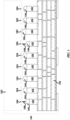
- FIG. 1 illustrates, by way of example, a cross-section diagram of an embodiment of an integrated circuit (IC) package 100 prior to attaching a die 103 to a substrate 101.
- Variation in height of conductive pillars 102 on the substrate 101 causes gaps 108 to form between a conductive ball 106 and a contact pad 104 of the die 103.
- the gaps 108 can cause electrical shorts, such as where the conductive ball 106, after reflow, does not span the entirety of the gap 108.
- the gaps 108 can cause the die 103 to be misaligned, such as by causing a shift or rotation in the die 103 relative to the substrate 101 after the die 103 is situated on one or more of the conductive bumps 106.
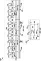
- FIG. 2A illustrates, by way of example, a cross-section diagram of an embodiment of a device 200A.
- the device 200A as illustrated includes a substrate 201 with conductive pillars 202 situated on landing pads 204 of the substrate 201.
- the device 200A as illustrated includes interconnect circuitry 204 in and/or on the substrate 201.
- the device 200A as illustrated includes a landing pad 206 electrically connected to the interconnect circuitry 204 and on the substrate 201.
- the device 200A as illustrated includes a conductive pad 208, such as can be electrically and mechanically connected to a circuit, such as to electrically connect the device 200A to the circuit.
- the substrate 201 can include a bumpless buildup layer (BBUL) substrate or other substrate.
- the substrate 201 can be built-up by situating a dielectric (e.g., an Ajinomoto buildup film (ABF)), patterning the dielectric, adding conductive material to the patterned dielectric, patterning the conductive material, and repeating until the substrate is built.
- a dielectric e.g., an Ajinomoto buildup film (ABF)
- ABS Ajinomoto buildup film
- any number of buildup layers can be used in creating the substrate 201 and the layers can be of a variety of thicknesses.
- the conductive pillars 202 generally are made of copper, but can include other conductive material, such tin, cadmium, gold, silver, palladium, rhodium, copper, bronze, brass, lead, nickel silver, beryllium copper, nickel, combinations thereof, or the like.
- the conductive pillars 202 can be created by situating a thin seed layer of conductive material on the substrate, patterning the seed layer with photoresist, etching openings over each conductive pillar location, plating conductive material in the openings in the photoresist, removing the photoresist, and then etching the seed layer that was protected by the photoresist (e.g., where the conductive pillars are not present).
- the conductive pillars 202 each include a respective height 210A, 210B, 210C, 210D, 210E, 210F, 210G, 210H, and 210I.
- a difference in the heights 210A-H can cause chip attach problems in later processing, such as is described with regard to FIG. 1 , among others.
- the conductive pillars 202 can be grown to include a height that is greater than a final height of the pillars, such as to allow the conductive pillars 202 to be planarized prior to die attach. In one or more embodiments, the conductive pillars 202 can be grown to be thirty (30) um or greater in height. Some embodiments may include conductive pillars that are shorter than 30 um.
- the interconnect circuitry 204 can provide electrical pathways through the substrate 201.
- the interconnect circuitry 204 can provide an electrical pathway for current to flow between a die attached to conductive pillars 202 and contact pads 208.
- the interconnect circuitry 204 can include electrical routing, such as can include, traces, planes, redistribution layer interconnect circuitry, vias, contact pads, or the like.
- the interconnect circuitry 204 can include conductive material, such as conductive material previously discussed with regard to the conductive pillars 202.
- the landing pads 206 are electrically connected to the interconnect circuitry 204.
- the landing pads 206 can be made of conductive material, such as conductive material previously discussed with regard to the conductive pillars.
- the landing pads 206 provide a location at which to electrically and mechanically connect a conductive pillar 202 to the interconnect circuitry 204.
- the contact pads 208 are electrically connected to the interconnect circuitry 204.
- the contact pads 208 provide electrical signals from the interconnect circuitry 204 to an external device (e.g., a printed circuit board (PCB), such as a flexible or rigid PCB, another package, a die, or other device).
- PCB printed circuit board
- the contact pads 208 can include conductive material, such as conductive material previously discussed with regard to the conductive pillars 202.
- FIG. 2B illustrates, by way of example, a cross-section diagram of an embodiment of a device 200B that includes the device 200A after a molding material 212 is situated on the substrate 201 and the conductive pillars 202.
- the molding material 212 can be situated over and around exposed portions of the conductive pillars 202, the substrate 201, and/or the landing pads 206.
- a height 213 of the molding material 212 can be greater than a height of the tallest conductive pillar 202 (e.g., greater than height 210H in the example of the device 200A).
- the molding material 212 can include a polymer, prepreg, and/or a material that is photo-imageable (i.e.
- the mold material 212 can be chosen based on chemical, electrical, mechanical, or manufacturing properties of the mold material 212.
- the molding material 212 is generally a dielectric insulator.
- FIG. 2C illustrates, by way of example, a cross-section diagram of an embodiment of a device 200C that includes the device 200B after the molding material 212 and the conductive pillars 202 are ground.
- Grinding the conductive pillars 202 forms conductive pillars 214 with more uniform heights 216A, 216B, 216C, 216D, 216E, 216F, 216G, 216H, and 216I than the conductive pillars 202 (i.e. the heights 210A-I).
- the grinding forms a molding material 218 that includes a height (generally the same as the heights 216A-I) that is less than the height 213 of the molding material 212.
- the grinding can include a mechanical grinding.
- the heights of the molding material 218 and the conductive pillar 214 can be generally uniform (e.g., within about 5 um of uniform) after the grinding process. That is a maximum height variation between any two points across the surface that was ground is at most 5 um
- FIG. 2D illustrates, by way of example, a cross-section diagram of an embodiment of a device 200D that includes the device 200C after a soft etch (e.g., a chemical etch) has removed a portion of the conductive pillars 214 to form the pillars 220.
- a soft etch e.g., a chemical etch
- the amount of material removed from the conductive pillars 214 can be controlled by an amount of time the conductive pillars 214 are exposed to a chemical and/or a concentration of the etching agent in the chemical.
- a height 222A, 222B, 222C, 222D, 222E, 222F, 222G, 222H, and 222I of the conductive pillars 220 is less than the respective height 216A-I of the conductive pillars 214.
- the height 222A-I of the conductive pillars 220 is less than the height of the molding material 218, which is generally the same as the height 216A-I.
- Reducing the height of the conductive pillar 220 can introduce greater variation in the co-planarity of the conductive pillars 220, but generally does not affect the co-planarity of the molding material 218.
- Reducing the height of the conductive pillars 214 can recess the conductive pillars 220, such that they include a height 222A-I that is less than a height of the molding material 218. Reducing the height of the conductive pillars 214 can help increase a bond strength between a conductive adhesive (see FIG. 2E ) and the conductive pillar 220.
- FIG. 2E illustrates, by way of example, a cross-section diagram of an embodiment of a device 200E that includes the device 200D after conductive adhesive 224 has been situated on and connected to the conductive pillars 220.
- the soft etch of the conductive pillars 214 can remove oxidation or other material from a contact surface of the conductive pillars 214, such as to form conductive pillars with a surface that is more amenable to forming a reliable electrical and/or mechanical connection with the conductive adhesive 224.
- the conductive adhesive 224 will form an electrical connection between the conductive pillars 220 and interconnect circuitry of a die (see FIG. 2F ).
- the conductive adhesive 224 can include solder (e.g., solder balls), a conductive paste, or other conductive material that can form an electrical and mechanical bond between the conductive pillars 220 and contact pads of the die (see FIG. 2F ).
- the conductive adhesive 224 can be situated by forming a mask that cover the molding material 218 and leaves the conductive pillars 220 exposed.
- the conductive adhesive 224 can be situated on the exposed conductive pillars 220 through the holes in the mask.
- the conductive adhesive 224 can be heated, such as to flow or at least partially cure the conductive adhesive 224 and bond the conductive adhesive 224 to the conductive pillar 220.
- FIG. 2F illustrates, by way of example, a cross-section diagram of an embodiment of a device 200F that includes the device 200E as a die 226 is being situated on the conductive adhesive 224.
- the conductive adhesive 224 can be softened, such as by heating the conductive adhesive 224, and hardened to form an electrical and mechanical connection between a contact pad 228 of the die 226 and the conductive pillars 220.
- FIG. 2G illustrates, by way of example, a cross-section diagram of an embodiment of an IC package 200G that includes the device 200F after the die 226 is electrically and mechanically connected to the conductive pillars 220 through the conductive adhesive 224.
- FIG. 2H illustrates, by way of example, an exploded view diagram of the dashed box labelled " FIG. 2H " in FIG. 2G .
- the conductive adhesive 224 is on the conductive pillar 220.
- the conductive adhesive 224 is over and in contact with a top surface 230 of the mold material 218.
- the conductive adhesive 224 fills the area that was occupied by the conductive pillar 214 prior to the soft etch.
- the conductive adhesive lines a portion of a sidewall 232 that extends beyond a top surface 234 of the conductive pillar 220.
- FIG. 3A illustrates, by way of example, a cross-section diagram of an embodiment of a device 300A that includes the device 200C depicted in FIG. 2C after some of the molding material 218 is removed to form the molding material 302.
- the molding material 302 has a height 304 that is less than the height 216A-I.
- the molding material 218 can be removed using photo-imaging, laser ablation, or other process.
- the molding material 302 can be recessed in embodiments in which the conductive adhesive 224 is attached to the die 226 prior to electrically and mechanically connecting the die 226 to the substrate 201, such as through the conductive pillars 214.
- FIG. 3B illustrates, by way of example, a cross-section diagram of an embodiment of a device 300B that includes the device 300A as a die 226 and the conductive adhesive 224 are being situated thereon.
- the conductive adhesive 224 can be softened, such as by heating the conductive adhesive 224, and hardened to form an electrical and mechanical connection between a contact pad 228 of the die 226 and the conductive pillars 214.
- FIG. 3C illustrates, by way of example, a cross-section diagram of an embodiment of an IC package 300C that includes the device 300B after the die 226 is electrically and mechanically connected to the conductive pillars 214 through the conductive adhesive 224.
- FIG. 3D illustrates, by way of example, an exploded view diagram of the dashed box labelled " FIG. 3D " in FIG. 3C .
- the conductive adhesive 224 is on the conductive pillar 214.
- the conductive adhesive 224 is on and in contact with sidewalls 306A and 306B of the conductive pillar 214.
- the conductive adhesive 224 fills the area that was occupied by the conductive pillar 214 prior to the soft etch.
- the conductive adhesive 224 extends beyond the sidewalls 306A-B of the conductive pillar 214, such as to overhang the conductive pillar 224.
- FIG. 4A illustrates, by way of example, a cross-section diagram of an embodiment of a device 400A that includes the device 200C depicted in FIG. 2C after a contact pads 402 are formed on respective conductive pillars 214.
- the contact pads 402 can be used in, for example, instances in which a width 408 (see FIG. 4D ) of the conductive pillar 214 is too small to support a direct connection to the conductive adhesive 224.
- the contact pad 402 can be created by situating a layer of conductive material on the conductive pillars 214 and molding material 218, a patterned mask can then be situated on the conductive material, the conductive material can be etched and the mask can be removed.
- a width 404 of the contact pad 402 can be greater than a width 406 of the landing pad 206. Having a narrower landing pad width 406 can help increase I/O density in the substrate 101.
- FIG. 4B illustrates, by way of example, a cross-section diagram of an embodiment of a device 400B that includes the device 400A after a conductive adhesive 224 is situated on respective contact pads 402 and as a die 226 being situated on the conductive adhesive.
- the conductive adhesive 224 can be softened, such as by heating the conductive adhesive 224, and hardened to form an electrical and mechanical connection between a contact pad 228 of the die 226 and the contact pad 402.
- FIG. 4C illustrates, by way of example, a cross-section diagram of an embodiment of an IC package 400C that includes the device 400B after the die 226 is electrically and mechanically connected to the conductive pillars 214 through the conductive adhesive 224 and the contact pad 402.
- FIG. 4D illustrates, by way of example, an exploded view diagram of the dashed box labelled " FIG. 3D " in FIG. 3C .
- the conductive adhesive 224 is on the conductive pillar 214.
- the conductive adhesive 224 is on and in contact with sidewalls 306A and 306B of the conductive pillar 214.
- the conductive adhesive 224 fills the area that was occupied by the conductive pillar 214 prior to the soft etch.
- the conductive adhesive 224 extends beyond the sidewalls 306A-B of the conductive pillar 214, such as to overhang the conductive pillar 224.
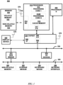
- FIG. 5 illustrates, by way of example, a logical block diagram of an embodiment of system 500.
- system 500 includes one or more components that can include a package with planar interconnects as discussed herein.
- processor 510 has one or more processing cores 512 and 512N, where 512N represents the Nth processor core inside processor 510 where N is a positive integer.
- system 500 includes multiple processors including 510 and 505, where processor 505 has logic similar or identical to the logic of processor 510.
- processing core 512 includes, but is not limited to, pre-fetch logic to fetch instructions, decode logic to decode the instructions, execution logic to execute instructions and the like.
- processor 510 has a cache memory 516 to cache instructions and/or data for system 500. Cache memory 516 may be organized into a hierarchal structure including one or more levels of cache memory.
- processor 510 includes a memory controller 514, which is operable to perform functions that enable the processor 510 to access and communicate with memory 530 that includes a volatile memory 532 and/or a non-volatile memory 534.
- processor 510 is coupled with memory 530 and chipset 520.
- Processor 510 may also be coupled to a wireless antenna 578 to communicate with any device configured to transmit and/or receive wireless signals.
- the wireless antenna interface 578 operates in accordance with, but is not limited to, the IEEE 802.11 standard and its related family, Home Plug AV (HPAV), Ultra Wide Band (UWB), Bluetooth, WiMax, or any form of wireless communication protocol.
- volatile memory 532 includes, but is not limited to, Synchronous Dynamic Random Access Memory (SDRAM), Dynamic Random Access Memory (DRAM), RAMBUS Dynamic Random Access Memory (RDRAM), and/or any other type of random access memory device.
- Non-volatile memory 534 includes, but is not limited to, flash memory, phase change memory (PCM), read-only memory (ROM), electrically erasable programmable read-only memory (EEPROM), or any other type of non-volatile memory device.
- Memory 530 stores information and instructions to be executed by processor 510. In one embodiment, memory 530 may also store temporary variables or other intermediate information while processor 510 is executing instructions.
- chipset 520 connects with processor 510 via Point-to-Point (PtP or P-P) interfaces 517 and 522.
- PtP Point-to-Point
- Chipset 520 enables processor 510 to connect to other elements in system 500.
- interfaces 517 and 522 operate in accordance with a PtP communication protocol such as the Intel ® QuickPath Interconnect (QPI) or the like. In other embodiments, a different interconnect may be used.
- chipset 520 is operable to communicate with processor 510, 505N, display device 540, and other devices.
- Chipset 520 may also be coupled to a wireless antenna 578 to communicate with any device configured to transmit and/or receive wireless signals.
- Chipset 520 connects to display device 540 via interface 526.
- Display 540 may be, for example, a liquid crystal display (LCD), a plasma display, cathode ray tube (CRT) display, or any other form of visual display device.
- processor 510 and chipset 520 are merged into a single SOC.
- chipset 520 connects to one or more buses 550 and 555 that interconnect various elements 574, 560, 562, 564, and 566. Buses 550 and 555 may be interconnected together via a bus bridge 572.
- chipset 520 couples with a non-volatile memory 560, a mass storage device(s) 562, a keyboard/mouse 564, and a network interface 566 via interface 524 and/or 504, etc.
- mass storage device 562 includes, but is not limited to, a solid state drive, a hard disk drive, a universal serial bus flash memory drive, or any other form of computer data storage medium.
- network interface 566 is implemented by any type of well-known network interface standard including, but not limited to, an Ethernet interface, a universal serial bus (USB) interface, a Peripheral Component Interconnect (PCI) Express interface, a wireless interface and/or any other suitable type of interface.
- the wireless interface operates in accordance with, but is not limited to, the IEEE 802.11 standard and its related family, Home Plug AV (HPAV), Ultra Wide Band (UWB), Bluetooth, WiMax, or any form of wireless communication protocol. While the components shown in FIG.
- cache memory 516 is depicted as a separate block within processor 510, cache memory 516 (or selected aspects of 516) can be incorporated into processor core 512.
- Example 1 a method of making an integrated circuit package includes growing conductive pillars on respective exposed landing pads of a substrate, situating molding material around and on the grown conductive pillars, removing, simultaneously, a portion of the grown conductive pillars and the molding material to make the grown conductive pillars and the molding material about planar, and electrically coupling a die to the conductive pillars.
- Example 1 can further include after removing the portion of the grown conductive pillars and the molding material, removing another portion of the conductive pillars to recess the conductive pillars in the molding material.
- Example 2 can further include, wherein removing another portion of the conductive pillars includes etching the conductive pillars.
- Example 2 can further include situating conductive adhesive on each of the conductive pillars before electrically connecting the die to the substrate.
- Example 4 can further include, wherein electrically connecting the die to the conductive pillars includes reflowing the conductive adhesive to electrically connect a contact pad of the die to a respective conductive pillar of the conductive pillars.
- Example 5 can further include, wherein the conductive adhesive, after reflowing, lines a portion of sidewalls and a portion of a surface of the molding material.
- Example 7 at least one of Examples 1-6 after removing the portion of the grown conductive pillars and the molding material, removing another portion of the molding material to recess the molding material relative to the conductive pillars.
- Example 7 can further include, wherein removing another portion of the molding material includes photo-imaging the molding material.
- Example 7 can further include situating conductive adhesive on the die before electrically connecting the die to the substrate.
- Example 9 can further include, wherein electrically connecting the die to the conductive pillars includes reflowing the conductive adhesive to electrically connect a contact pad of the die to a respective conductive pillar of the conductive pillars.
- Example 10 can further include, wherein the conductive adhesive, after reflowing, lines exposed portions of sidewalls of the conductive pillars.
- Example 12 at least one of Examples 1-11 can further include after removing the portion of the grown conductive pillars and the molding material, forming contact pads on respective conductive pillars.
- Example 12 can further include, wherein forming the contact pads includes forming the contact pads to include a width greater than a width of the landing pads.
- Example 13 can further include situating conductive adhesive on each of the contact pads before electrically connecting the die to the substrate.
- an IC package includes a substrate comprising interconnect circuitry embedded in buildup layers and a plurality of landing pads exposed at a top surface thereof, a plurality of conductive pillars electrically connected to respective landing pads, a molding material around at least a portion of sidewall of the conductive pillars and on the substrate, and a die on the substrate, the die including contact pads electrically coupled to the interconnect circuitry through the conductive pillars, wherein the conductive pillars each include top surfaces that are generally planar with respect to one another to within a five micron deviation.
- Example 15 can further include, wherein the contact pads of the die are first contact pads and the package further comprises second contact pads connected to respective conductive pillars, the second contact pads including a width greater than the landing pads, the second contact pads situated between the conductive pillars and the first contact pads.
- Example 15 can further include, wherein the conductive pillars include a height that is greater than a height of the molding material and the IC package further comprises a conductive adhesive electrically connecting the first contact pads to the conductive pillars, wherein the conductive adhesive is in contact with sidewalls of the conductive pillars.
- Example 15 can further include, wherein the conductive pillars include a height that is less than a height of the molding material and the IC package further comprises a conductive adhesive electrically connecting the first contact pads to the conductive pillars, wherein the conductive adhesive is in contact with sidewalls of the molding material.
- a method of making an integrated circuit package can include growing copper pillars on respective exposed landing pads of a substrate, situating molding material around and on the grown copper pillars, removing, simultaneously, a portion of the grown copper pillars and the molding material to make the grown copper pillars planar with respect to each other to within a five micron deviation, and reflowing solder balls to electrically couple contact pads of the die to the copper pillars and to interconnect circuitry of the substrate.
- Example 19 can further include after removing the portion of the grown copper pillars and the molding material, etching another portion of the copper pillars to recess the copper pillars in the molding material, attaching the solder balls to respective copper pillars before reflowing the solder balls, and wherein the solder balls after reflowing, line a portion of sidewalls and a portion of a surface of the molding material.
- Example 19 can further include after removing the portion of the grown conductive pillars and the molding material, removing another portion of the molding material to recess the molding material relative to the conductive pillars.
- Example 21 can further include, wherein removing another portion of the molding material includes photo-imaging the molding material.
- Example 21 can further include situating conductive adhesive on the die before electrically connecting the die to the substrate.
- Example 23 can further include, wherein electrically connecting the die to the conductive pillars includes reflowing the conductive adhesive to electrically connect a contact pad of the die to a respective conductive pillar of the conductive pillars.
- Example 24 can further include, wherein the conductive adhesive, after reflowing, lines exposed portions of sidewalls of the conductive pillars.
- Example 25 can further include after removing the portion of the grown conductive pillars and the molding material, forming contact pads on respective conductive pillars.
- Example 26 can further include, wherein forming the contact pads includes forming the contact pads to include a width greater than a width of the landing pads.
- Example 27 can further include situating conductive adhesive on each of the contact pads before electrically connecting the die to the substrate.
Landscapes
- Wire Bonding (AREA)
- Physics & Mathematics (AREA)
- Geometry (AREA)
- Internal Circuitry In Semiconductor Integrated Circuit Devices (AREA)
Abstract
Description
- This patent application claims the benefit of priority to
U.S. Application Serial No. 15/198,107, filed June 30, 2016 - Examples generally relate to integrated circuit (IC) packages, and more specifically to processes for creating an IC package that includes generally planar conductive columns and the devices resulting from such processes.
- IC package technology has a tendency to move towards making ICs smaller and smaller. The smaller IC packages generally include more signal routing per unit area than larger IC packages. Manufacturing such smaller packages can be challenging. Smaller packages can include a higher yield loss than larger packages.
- In the drawings, which are not necessarily drawn to scale, like numerals may describe similar components in different views. Like numerals having different letter suffixes may represent different instances of similar components. The drawings illustrate generally, by way of example, but not by way of limitation, various embodiments discussed in the present document.
-
FIG. 1 illustrates, by way of example, a cross-section diagram of an example of an IC package. -
FIGS. 2A-2H illustrate, by way of example, cross-section diagrams of stages of an example of a process of creating an IC package. -
FIGS. 3A-3D illustrate, by way of example, cross-section diagrams of stages of an example of another process for creating an IC package. -
FIGS. 4A-4D illustrate, by way of example, cross-section diagrams of stages of an example of another process for creating an IC package. -
FIG. 5 illustrates, by way of example, a schematic diagram of an example of an electronic system. - Examples in this disclosure relate to processes for creating IC packages with conductive pillars that are generally planar (e.g., to within about five (5) um of each other or less). Examples also relate to apparatuses and systems created using such processes.
- The following description includes terms, such as upper, lower, first, second, etc. that are used for descriptive purposes only and are not to be construed as limiting. The examples of an apparatus or article described herein can be manufactured, used, or shipped in a number of positions and orientations. The terms "die" and "chip" generally refer to the physical object that is the basic workpiece that is transformed by various process operations into the desired integrated circuit device. A die is usually singulated from a wafer and wafers may be made of semiconducting, non-semiconducting, or combinations of semiconducting and non-semiconducting materials.
- As IC package interconnects (e.g., flip chip or other interconnects) continue to scale to finer pitches, the ability of the solder used in/on an interconnect to provide room for random or systematic fluctuations in bump height or surface co-planarity becomes more limited. Discussed herein are processes for creating an IC package with conductive pillars that are generally co-planar. The generally co-planar conductive pillars can help increase manufacturing yields, such as by reducing a variation in a gap between the conductive pillar and a chip to be attached to the pillar. The generally co-planar conductive pillars can help make pitch scaling more feasible. Finer pitches can be tolerated due to the more predictable gap distance between a respective conductive pillar and a pad to which the conductive pillar is to be connected.
- In a high level summary, the process can include creating a conductive pillar (e.g., about forty (40) um tall in some manufacturing processes) on each bump location on a surface of a package substrate. The substrate can be covered with a mold compound thicker than the height of the conductive pillar, such that the mold compound extends beyond and covers the conductive pillar. The conductive pillars can then be exposed, such as through a controlled grinding process that can remove a specified amount of the mold (e.g., several microns of the mold). After grinding, conductive adhesive material (e.g., a solder ball, solder, or paste, among others) can be attached to the pillar or the pillar can be capped with a patterned pad and then the conductive adhesive can be added to the pad. A die can then be attached to the conductive pillars, such as through the conductive adhesive material.
- Current substrate conductive pillar co-planarity combined with current substrate warpage can result in height variations between about ten (10) um and twenty (20) um across a die attach area on a package. This variation makes chip attach difficult and can negatively impact package yields. This variation also compromises advantages in die placement precision and accuracy achieved by a thermocompression bonding (TCB) tool. Embodiments discussed herein can help create absolute height variations less than (or equal to) five (5) um across the surfaces of conductive pillars. Such co-planarity can help enable a high yielding TCB chip attach process, such as at pitches of less than one hundred thirty (130) um. Further, such co-planarity can help reduce the size of the substrate landing pad under the conductive pillars. Reducing the size of the landing pad can help increase I/O routing density, such as without modifying a substrate patterning process.
- Reference will now be made to the drawings wherein like structures will be provided with like suffix reference designations. In order to show the structures of various examples clearly, the drawings included herein are diagrammatic representations of integrated circuit structures. Thus, the actual appearance of the fabricated structures, for example in a photomicrograph, may appear different while still incorporating subject matter of the illustrated examples. Moreover, the drawings show the structures to aid in understanding the illustrated examples.
-
FIG. 1 illustrates, by way of example, a cross-section diagram of an embodiment of an integrated circuit (IC)package 100 prior to attaching a die 103 to asubstrate 101. Variation in height ofconductive pillars 102 on thesubstrate 101 causesgaps 108 to form between aconductive ball 106 and acontact pad 104 of thedie 103. Thegaps 108 can cause electrical shorts, such as where theconductive ball 106, after reflow, does not span the entirety of thegap 108. Thegaps 108 can cause thedie 103 to be misaligned, such as by causing a shift or rotation in the die 103 relative to thesubstrate 101 after the die 103 is situated on one or more of theconductive bumps 106. -
FIG. 2A illustrates, by way of example, a cross-section diagram of an embodiment of adevice 200A. Thedevice 200A as illustrated includes asubstrate 201 withconductive pillars 202 situated onlanding pads 204 of thesubstrate 201. Thedevice 200A as illustrated includesinterconnect circuitry 204 in and/or on thesubstrate 201. Thedevice 200A as illustrated includes alanding pad 206 electrically connected to theinterconnect circuitry 204 and on thesubstrate 201. Thedevice 200A as illustrated includes aconductive pad 208, such as can be electrically and mechanically connected to a circuit, such as to electrically connect thedevice 200A to the circuit. - In one or more embodiments, the
substrate 201 can include a bumpless buildup layer (BBUL) substrate or other substrate. Thesubstrate 201 can be built-up by situating a dielectric (e.g., an Ajinomoto buildup film (ABF)), patterning the dielectric, adding conductive material to the patterned dielectric, patterning the conductive material, and repeating until the substrate is built. Generally, any number of buildup layers can be used in creating thesubstrate 201 and the layers can be of a variety of thicknesses. - The
conductive pillars 202 generally are made of copper, but can include other conductive material, such tin, cadmium, gold, silver, palladium, rhodium, copper, bronze, brass, lead, nickel silver, beryllium copper, nickel, combinations thereof, or the like. Theconductive pillars 202 can be created by situating a thin seed layer of conductive material on the substrate, patterning the seed layer with photoresist, etching openings over each conductive pillar location, plating conductive material in the openings in the photoresist, removing the photoresist, and then etching the seed layer that was protected by the photoresist (e.g., where the conductive pillars are not present). - The
conductive pillars 202 each include arespective height heights 210A-H can cause chip attach problems in later processing, such as is described with regard toFIG. 1 , among others. To help alleviate the problems with the chip attach, it can be beneficial to make theheights 210A-H more uniform, such as to reduce a distance between a conductive ball on the conductive pillar and an exposed surface of a contact pad of a die to be attached to the conductive pillar (seeFIGS. 2E and 2F ). - The
conductive pillars 202 can be grown to include a height that is greater than a final height of the pillars, such as to allow theconductive pillars 202 to be planarized prior to die attach. In one or more embodiments, theconductive pillars 202 can be grown to be thirty (30) um or greater in height. Some embodiments may include conductive pillars that are shorter than 30 um. - The
interconnect circuitry 204 can provide electrical pathways through thesubstrate 201. Theinterconnect circuitry 204 can provide an electrical pathway for current to flow between a die attached toconductive pillars 202 andcontact pads 208. Theinterconnect circuitry 204 can include electrical routing, such as can include, traces, planes, redistribution layer interconnect circuitry, vias, contact pads, or the like. Theinterconnect circuitry 204 can include conductive material, such as conductive material previously discussed with regard to theconductive pillars 202. - The
landing pads 206 are electrically connected to theinterconnect circuitry 204. Thelanding pads 206 can be made of conductive material, such as conductive material previously discussed with regard to the conductive pillars. Thelanding pads 206 provide a location at which to electrically and mechanically connect aconductive pillar 202 to theinterconnect circuitry 204. - The
contact pads 208 are electrically connected to theinterconnect circuitry 204. Thecontact pads 208 provide electrical signals from theinterconnect circuitry 204 to an external device (e.g., a printed circuit board (PCB), such as a flexible or rigid PCB, another package, a die, or other device). Thecontact pads 208 can include conductive material, such as conductive material previously discussed with regard to theconductive pillars 202. -
FIG. 2B illustrates, by way of example, a cross-section diagram of an embodiment of adevice 200B that includes thedevice 200A after amolding material 212 is situated on thesubstrate 201 and theconductive pillars 202. Themolding material 212 can be situated over and around exposed portions of theconductive pillars 202, thesubstrate 201, and/or thelanding pads 206. Aheight 213 of themolding material 212 can be greater than a height of the tallest conductive pillar 202 (e.g., greater thanheight 210H in the example of thedevice 200A). Themolding material 212 can include a polymer, prepreg, and/or a material that is photo-imageable (i.e. a material that can be removed using a photo-imaging process), such as polyimide. Themold material 212 can be chosen based on chemical, electrical, mechanical, or manufacturing properties of themold material 212. Themolding material 212 is generally a dielectric insulator. -
FIG. 2C illustrates, by way of example, a cross-section diagram of an embodiment of adevice 200C that includes thedevice 200B after themolding material 212 and theconductive pillars 202 are ground. Grinding theconductive pillars 202 forms conductivepillars 214 with moreuniform heights heights 210A-I). The grinding forms amolding material 218 that includes a height (generally the same as theheights 216A-I) that is less than theheight 213 of themolding material 212. The grinding can include a mechanical grinding. The heights of themolding material 218 and theconductive pillar 214 can be generally uniform (e.g., within about 5 um of uniform) after the grinding process. That is a maximum height variation between any two points across the surface that was ground is at most 5 um. -
FIG. 2D illustrates, by way of example, a cross-section diagram of an embodiment of adevice 200D that includes thedevice 200C after a soft etch (e.g., a chemical etch) has removed a portion of theconductive pillars 214 to form thepillars 220. The amount of material removed from theconductive pillars 214 can be controlled by an amount of time theconductive pillars 214 are exposed to a chemical and/or a concentration of the etching agent in the chemical. Aheight conductive pillars 220 is less than therespective height 216A-I of theconductive pillars 214. Theheight 222A-I of theconductive pillars 220 is less than the height of themolding material 218, which is generally the same as theheight 216A-I. - Reducing the height of the
conductive pillar 220 can introduce greater variation in the co-planarity of theconductive pillars 220, but generally does not affect the co-planarity of themolding material 218. Reducing the height of theconductive pillars 214 can recess theconductive pillars 220, such that they include aheight 222A-I that is less than a height of themolding material 218. Reducing the height of theconductive pillars 214 can help increase a bond strength between a conductive adhesive (seeFIG. 2E ) and theconductive pillar 220. -
FIG. 2E illustrates, by way of example, a cross-section diagram of an embodiment of adevice 200E that includes thedevice 200D afterconductive adhesive 224 has been situated on and connected to theconductive pillars 220. The soft etch of theconductive pillars 214 can remove oxidation or other material from a contact surface of theconductive pillars 214, such as to form conductive pillars with a surface that is more amenable to forming a reliable electrical and/or mechanical connection with theconductive adhesive 224. Theconductive adhesive 224 will form an electrical connection between theconductive pillars 220 and interconnect circuitry of a die (seeFIG. 2F ). Theconductive adhesive 224 can include solder (e.g., solder balls), a conductive paste, or other conductive material that can form an electrical and mechanical bond between theconductive pillars 220 and contact pads of the die (seeFIG. 2F ). Theconductive adhesive 224 can be situated by forming a mask that cover themolding material 218 and leaves theconductive pillars 220 exposed. Theconductive adhesive 224 can be situated on the exposedconductive pillars 220 through the holes in the mask. Theconductive adhesive 224 can be heated, such as to flow or at least partially cure theconductive adhesive 224 and bond theconductive adhesive 224 to theconductive pillar 220. -
FIG. 2F illustrates, by way of example, a cross-section diagram of an embodiment of adevice 200F that includes thedevice 200E as adie 226 is being situated on theconductive adhesive 224. Theconductive adhesive 224 can be softened, such as by heating theconductive adhesive 224, and hardened to form an electrical and mechanical connection between acontact pad 228 of thedie 226 and theconductive pillars 220.FIG. 2G illustrates, by way of example, a cross-section diagram of an embodiment of anIC package 200G that includes thedevice 200F after thedie 226 is electrically and mechanically connected to theconductive pillars 220 through theconductive adhesive 224. -
FIG. 2H illustrates, by way of example, an exploded view diagram of the dashed box labelled "FIG. 2H " inFIG. 2G . Theconductive adhesive 224 is on theconductive pillar 220. Theconductive adhesive 224 is over and in contact with atop surface 230 of themold material 218. Theconductive adhesive 224 fills the area that was occupied by theconductive pillar 214 prior to the soft etch. The conductive adhesive lines a portion of asidewall 232 that extends beyond a top surface 234 of theconductive pillar 220. -
FIG. 3A illustrates, by way of example, a cross-section diagram of an embodiment of adevice 300A that includes thedevice 200C depicted inFIG. 2C after some of themolding material 218 is removed to form themolding material 302. Themolding material 302 has aheight 304 that is less than theheight 216A-I. Themolding material 218 can be removed using photo-imaging, laser ablation, or other process. Themolding material 302 can be recessed in embodiments in which theconductive adhesive 224 is attached to the die 226 prior to electrically and mechanically connecting thedie 226 to thesubstrate 201, such as through theconductive pillars 214. -
FIG. 3B illustrates, by way of example, a cross-section diagram of an embodiment of adevice 300B that includes thedevice 300A as adie 226 and theconductive adhesive 224 are being situated thereon. Theconductive adhesive 224 can be softened, such as by heating theconductive adhesive 224, and hardened to form an electrical and mechanical connection between acontact pad 228 of thedie 226 and theconductive pillars 214.FIG. 3C illustrates, by way of example, a cross-section diagram of an embodiment of anIC package 300C that includes thedevice 300B after thedie 226 is electrically and mechanically connected to theconductive pillars 214 through theconductive adhesive 224. -
FIG. 3D illustrates, by way of example, an exploded view diagram of the dashed box labelled "FIG. 3D " inFIG. 3C . Theconductive adhesive 224 is on theconductive pillar 214. Theconductive adhesive 224 is on and in contact withsidewalls conductive pillar 214. Theconductive adhesive 224 fills the area that was occupied by theconductive pillar 214 prior to the soft etch. Theconductive adhesive 224 extends beyond thesidewalls 306A-B of theconductive pillar 214, such as to overhang theconductive pillar 224. -
FIG. 4A illustrates, by way of example, a cross-section diagram of an embodiment of adevice 400A that includes thedevice 200C depicted inFIG. 2C after acontact pads 402 are formed on respectiveconductive pillars 214. Thecontact pads 402 can be used in, for example, instances in which a width 408 (seeFIG. 4D ) of theconductive pillar 214 is too small to support a direct connection to theconductive adhesive 224. Thecontact pad 402 can be created by situating a layer of conductive material on theconductive pillars 214 andmolding material 218, a patterned mask can then be situated on the conductive material, the conductive material can be etched and the mask can be removed. Awidth 404 of thecontact pad 402 can be greater than awidth 406 of thelanding pad 206. Having a narrowerlanding pad width 406 can help increase I/O density in thesubstrate 101. -
FIG. 4B illustrates, by way of example, a cross-section diagram of an embodiment of adevice 400B that includes thedevice 400A after aconductive adhesive 224 is situated onrespective contact pads 402 and as adie 226 being situated on the conductive adhesive. Theconductive adhesive 224 can be softened, such as by heating theconductive adhesive 224, and hardened to form an electrical and mechanical connection between acontact pad 228 of thedie 226 and thecontact pad 402.FIG. 4C illustrates, by way of example, a cross-section diagram of an embodiment of anIC package 400C that includes thedevice 400B after thedie 226 is electrically and mechanically connected to theconductive pillars 214 through theconductive adhesive 224 and thecontact pad 402. -
FIG. 4D illustrates, by way of example, an exploded view diagram of the dashed box labelled "FIG. 3D " inFIG. 3C . Theconductive adhesive 224 is on theconductive pillar 214. Theconductive adhesive 224 is on and in contact withsidewalls conductive pillar 214. Theconductive adhesive 224 fills the area that was occupied by theconductive pillar 214 prior to the soft etch. Theconductive adhesive 224 extends beyond thesidewalls 306A-B of theconductive pillar 214, such as to overhang theconductive pillar 224. -
FIG. 5 illustrates, by way of example, a logical block diagram of an embodiment ofsystem 500. In one or more embodiments,system 500 includes one or more components that can include a package with planar interconnects as discussed herein. - In one embodiment,
processor 510 has one ormore processing cores processor 510 where N is a positive integer. In one embodiment,system 500 includes multiple processors including 510 and 505, whereprocessor 505 has logic similar or identical to the logic ofprocessor 510. In some embodiments, processingcore 512 includes, but is not limited to, pre-fetch logic to fetch instructions, decode logic to decode the instructions, execution logic to execute instructions and the like. In some embodiments,processor 510 has acache memory 516 to cache instructions and/or data forsystem 500.Cache memory 516 may be organized into a hierarchal structure including one or more levels of cache memory. - In some embodiments,
processor 510 includes amemory controller 514, which is operable to perform functions that enable theprocessor 510 to access and communicate withmemory 530 that includes avolatile memory 532 and/or a non-volatile memory 534. In some embodiments,processor 510 is coupled withmemory 530 andchipset 520.Processor 510 may also be coupled to awireless antenna 578 to communicate with any device configured to transmit and/or receive wireless signals. In one embodiment, thewireless antenna interface 578 operates in accordance with, but is not limited to, the IEEE 802.11 standard and its related family, Home Plug AV (HPAV), Ultra Wide Band (UWB), Bluetooth, WiMax, or any form of wireless communication protocol. - In some embodiments,
volatile memory 532 includes, but is not limited to, Synchronous Dynamic Random Access Memory (SDRAM), Dynamic Random Access Memory (DRAM), RAMBUS Dynamic Random Access Memory (RDRAM), and/or any other type of random access memory device. Non-volatile memory 534 includes, but is not limited to, flash memory, phase change memory (PCM), read-only memory (ROM), electrically erasable programmable read-only memory (EEPROM), or any other type of non-volatile memory device. -
Memory 530 stores information and instructions to be executed byprocessor 510. In one embodiment,memory 530 may also store temporary variables or other intermediate information whileprocessor 510 is executing instructions. In the illustrated embodiment,chipset 520 connects withprocessor 510 via Point-to-Point (PtP or P-P) interfaces 517 and 522.Chipset 520 enablesprocessor 510 to connect to other elements insystem 500. In some embodiments of the invention, interfaces 517 and 522 operate in accordance with a PtP communication protocol such as the Intel® QuickPath Interconnect (QPI) or the like. In other embodiments, a different interconnect may be used. - In some embodiments,
chipset 520 is operable to communicate withprocessor 510, 505N,display device 540, and other devices.Chipset 520 may also be coupled to awireless antenna 578 to communicate with any device configured to transmit and/or receive wireless signals. -
Chipset 520 connects to displaydevice 540 viainterface 526.Display 540 may be, for example, a liquid crystal display (LCD), a plasma display, cathode ray tube (CRT) display, or any other form of visual display device. In some embodiments of the invention,processor 510 andchipset 520 are merged into a single SOC. In addition,chipset 520 connects to one ormore buses various elements Buses chipset 520 couples with anon-volatile memory 560, a mass storage device(s) 562, a keyboard/mouse 564, and anetwork interface 566 viainterface 524 and/or 504, etc. - In one embodiment,
mass storage device 562 includes, but is not limited to, a solid state drive, a hard disk drive, a universal serial bus flash memory drive, or any other form of computer data storage medium. In one embodiment,network interface 566 is implemented by any type of well-known network interface standard including, but not limited to, an Ethernet interface, a universal serial bus (USB) interface, a Peripheral Component Interconnect (PCI) Express interface, a wireless interface and/or any other suitable type of interface. In one embodiment, the wireless interface operates in accordance with, but is not limited to, the IEEE 802.11 standard and its related family, Home Plug AV (HPAV), Ultra Wide Band (UWB), Bluetooth, WiMax, or any form of wireless communication protocol.
While the components shown inFIG. 5 are depicted as separate blocks within thesystem 500, the functions performed by some of these blocks may be integrated within a single semiconductor circuit or may be implemented using two or more separate integrated circuits. For example, althoughcache memory 516 is depicted as a separate block withinprocessor 510, cache memory 516 (or selected aspects of 516) can be incorporated intoprocessor core 512. - The present subject matter may be described by way of several examples.
- In Example 1 a method of making an integrated circuit package includes growing conductive pillars on respective exposed landing pads of a substrate, situating molding material around and on the grown conductive pillars, removing, simultaneously, a portion of the grown conductive pillars and the molding material to make the grown conductive pillars and the molding material about planar, and electrically coupling a die to the conductive pillars.
- In Example 2, Example 1 can further include after removing the portion of the grown conductive pillars and the molding material, removing another portion of the conductive pillars to recess the conductive pillars in the molding material.
- In Example 3, Example 2 can further include, wherein removing another portion of the conductive pillars includes etching the conductive pillars.
- In Example 4, Example 2 can further include situating conductive adhesive on each of the conductive pillars before electrically connecting the die to the substrate.
- In Example 5, Example 4 can further include, wherein electrically connecting the die to the conductive pillars includes reflowing the conductive adhesive to electrically connect a contact pad of the die to a respective conductive pillar of the conductive pillars.
- In Example 6, Example 5 can further include, wherein the conductive adhesive, after reflowing, lines a portion of sidewalls and a portion of a surface of the molding material.
- In Example 7, at least one of Examples 1-6 after removing the portion of the grown conductive pillars and the molding material, removing another portion of the molding material to recess the molding material relative to the conductive pillars.
- In Example 8, Example 7 can further include, wherein removing another portion of the molding material includes photo-imaging the molding material.
- In Example 9, Example 7 can further include situating conductive adhesive on the die before electrically connecting the die to the substrate.
- In Example 10, Example 9 can further include, wherein electrically connecting the die to the conductive pillars includes reflowing the conductive adhesive to electrically connect a contact pad of the die to a respective conductive pillar of the conductive pillars.
- In Example 11, Example 10 can further include, wherein the conductive adhesive, after reflowing, lines exposed portions of sidewalls of the conductive pillars.
- In Example 12, at least one of Examples 1-11 can further include after removing the portion of the grown conductive pillars and the molding material, forming contact pads on respective conductive pillars.
- In Example 13, Example 12 can further include, wherein forming the contact pads includes forming the contact pads to include a width greater than a width of the landing pads.
- In Example 14, Example 13 can further include situating conductive adhesive on each of the contact pads before electrically connecting the die to the substrate.
- In Example 15 an IC package includes a substrate comprising interconnect circuitry embedded in buildup layers and a plurality of landing pads exposed at a top surface thereof, a plurality of conductive pillars electrically connected to respective landing pads, a molding material around at least a portion of sidewall of the conductive pillars and on the substrate, and a die on the substrate, the die including contact pads electrically coupled to the interconnect circuitry through the conductive pillars, wherein the conductive pillars each include top surfaces that are generally planar with respect to one another to within a five micron deviation.
- In Example 16, Example 15 can further include, wherein the contact pads of the die are first contact pads and the package further comprises second contact pads connected to respective conductive pillars, the second contact pads including a width greater than the landing pads, the second contact pads situated between the conductive pillars and the first contact pads.
- In Example 17, Example 15 can further include, wherein the conductive pillars include a height that is greater than a height of the molding material and the IC package further comprises a conductive adhesive electrically connecting the first contact pads to the conductive pillars, wherein the conductive adhesive is in contact with sidewalls of the conductive pillars.
- In Example 18, Example 15 can further include, wherein the conductive pillars include a height that is less than a height of the molding material and the IC package further comprises a conductive adhesive electrically connecting the first contact pads to the conductive pillars, wherein the conductive adhesive is in contact with sidewalls of the molding material.
- In Example 19 a method of making an integrated circuit package can include growing copper pillars on respective exposed landing pads of a substrate, situating molding material around and on the grown copper pillars, removing, simultaneously, a portion of the grown copper pillars and the molding material to make the grown copper pillars planar with respect to each other to within a five micron deviation, and reflowing solder balls to electrically couple contact pads of the die to the copper pillars and to interconnect circuitry of the substrate.
- In Example 20, Example 19 can further include after removing the portion of the grown copper pillars and the molding material, etching another portion of the copper pillars to recess the copper pillars in the molding material, attaching the solder balls to respective copper pillars before reflowing the solder balls, and wherein the solder balls after reflowing, line a portion of sidewalls and a portion of a surface of the molding material.
- In Example 21, Example 19 can further include after removing the portion of the grown conductive pillars and the molding material, removing another portion of the molding material to recess the molding material relative to the conductive pillars.
- In Example 22, Example 21 can further include, wherein removing another portion of the molding material includes photo-imaging the molding material.
- In Example 23, Example 21 can further include situating conductive adhesive on the die before electrically connecting the die to the substrate.
- In Example 24, Example 23 can further include, wherein electrically connecting the die to the conductive pillars includes reflowing the conductive adhesive to electrically connect a contact pad of the die to a respective conductive pillar of the conductive pillars.
- In Example 25, Example 24 can further include, wherein the conductive adhesive, after reflowing, lines exposed portions of sidewalls of the conductive pillars.
- In Example 26, Example 25 can further include after removing the portion of the grown conductive pillars and the molding material, forming contact pads on respective conductive pillars.
- In Example 27, Example 26 can further include, wherein forming the contact pads includes forming the contact pads to include a width greater than a width of the landing pads.
- In Example 28, Example 27 can further include situating conductive adhesive on each of the contact pads before electrically connecting the die to the substrate.
- Each of these non-limiting examples can stand on its own, or can be combined in various permutations or combinations with one or more of the other examples.
- The above detailed description includes references to the accompanying drawings, which form a part of the detailed description. The drawings show, by way of illustration, specific embodiments in which methods, apparatuses, and systems discussed herein can be practiced. These embodiments are also referred to herein as "examples." Such examples can include elements in addition to those shown or described. However, the present inventors also contemplate examples in which only those elements shown or described are provided. Moreover, the present inventors also contemplate examples using any combination or permutation of those elements shown or described (or one or more aspects thereof), either with respect to a particular example (or one or more aspects thereof), or with respect to other examples (or one or more aspects thereof) shown or described herein.
- In this document, the terms "a" or "an" are used, as is common in patent documents, to include one or more than one, independent of any other instances or usages of "at least one" or "one or more." In this document, the term "or" is used to refer to a nonexclusive or, such that "A or B" includes "A but not B," "B but not A," and "A and B," unless otherwise indicated. In this document, the terms "including" and "in which" are used as the plain-English equivalents of the respective terms "comprising" and "wherein." Also, in the following claims, the terms "including" and "comprising" are open-ended, that is, a system, device, article, composition, formulation, or process that includes elements in addition to those listed after such a term in a claim are still deemed to fall within the scope of that claim. Moreover, in the following claims, the terms "first," "second," and "third," etc. are used merely as labels, and are not intended to impose numerical requirements on their objects.
- The above description is intended to be illustrative, and not restrictive. For example, the above-described examples (or one or more aspects thereof) may be used in combination with each other. Other embodiments can be used, such as by one of ordinary skill in the art upon reviewing the above description. The Abstract is provided to allow the reader to quickly ascertain the nature of the technical disclosure. It is submitted with the understanding that it will not be used to interpret or limit the scope or meaning of the claims. Also, in the above Detailed Description, various features may be grouped together to streamline the disclosure. This should not be interpreted as intending that an unclaimed disclosed feature is essential to any claim. Rather, inventive subject matter may lie in less than all features of a particular disclosed embodiment. Thus, the following claims are hereby incorporated into the Detailed Description as examples or embodiments, with each claim standing on its own as a separate embodiment, and it is contemplated that such embodiments can be combined with each other in various combinations or permutations. The scope of the invention should be determined with reference to the appended claims, along with the full scope of equivalents to which such claims are entitled.
Claims (15)
- An integrated circuit (IC) package comprising:a substrate comprising electrical pathways;a plurality of landing pads at a top surface of the substrate;a plurality of conductive pillars electrically connected to respective landing pads, each of the conductive pillars having a height less than 30 micrometers, wherein the heights of the plurality of conductive pillars are within five micrometers of each other;an insulating material between adjacent ones of the plurality of conductive pillars, wherein a height of the insulating material is within 5 micrometers of the height of one of the conductive pillars; anda die electrically coupled to the plurality of conductive pillars.
- The IC package of claim 1, wherein the IC package comprises at least four conductive pillars.
- The IC package of one of the previous claims, wherein the die is electrically coupled to the electrical pathways in the substrate via the conductive pillars and the landing pads.
- The IC package of one of the previous claims, wherein each of the plurality of conductive pillars is coupled to a conductive adhesive.
- The IC package of claim 4, wherein the conductive adhesive is between one of the conductive pillars and the die.
- The IC package of claim 4 or 5, wherein the conductive adhesive is solder.
- The IC package of claim 6, wherein, for each of the conductive pillars, a portion of the solder extends along a sidewall of the conductive pillar.
- The IC package of one of the previous claims, wherein the plurality of conductive pillars include copper.
- The IC package of one of the previous claims, wherein the substrate comprises a plurality of contact pads on a bottom surface of the substrate, the bottom surface opposite the top surface.
- The IC package of one of the previous claims, wherein the die comprises contact pads electrically coupled to the plurality of conductive pillars.
- A package comprising:a substrate comprising:a first surface having a plurality of contact pads;a second surface opposite the first surface, the second surface having a plurality of landing pads; andan electrical pathway between one of the contact pads and one of the landing pads;a plurality of conductive pillars electrically connected to respective ones of the plurality of landing pads, wherein heights of the plurality of conductive pillars are within five micrometers of each other;an insulating material between adjacent ones of the plurality of conductive pillars, wherein a height of the insulating material is within 5 micrometers of the height of one of the conductive pillars; anda die electrically coupled to the plurality of conductive pillars.
- The package of claim 11, further comprising an external device coupled to the plurality of contact pads.
- The package of claim 12, wherein the external device is a circuit board.
- The package of claim 12 or 13, wherein the external device is a second die.
- The package of claim 11, 12, 13 or 14, wherein a width of one of the plurality of contact pads is greater than a width of one of the plurality of landing pads.
Applications Claiming Priority (3)
| Application Number | Priority Date | Filing Date | Title |
|---|---|---|---|
| US15/198,107 US10651116B2 (en) | 2016-06-30 | 2016-06-30 | Planar integrated circuit package interconnects |
| PCT/US2017/035795 WO2018005006A1 (en) | 2016-06-30 | 2017-06-02 | Sampler circuit with current injection for pre-amplification |
| EP17820867.4A EP3479400A4 (en) | 2016-06-30 | 2017-06-02 | PLANAR INTEGRATED CIRCUIT BOX INTERCONNECTIONS |
Related Parent Applications (1)
| Application Number | Title | Priority Date | Filing Date |
|---|---|---|---|
| EP17820867.4A Division EP3479400A4 (en) | 2016-06-30 | 2017-06-02 | PLANAR INTEGRATED CIRCUIT BOX INTERCONNECTIONS |
Publications (2)
| Publication Number | Publication Date |
|---|---|
| EP4521462A2 true EP4521462A2 (en) | 2025-03-12 |
| EP4521462A3 EP4521462A3 (en) | 2026-04-29 |
Family
ID=60786507
Family Applications (2)
| Application Number | Title | Priority Date | Filing Date |
|---|---|---|---|
| EP24223465.6A Pending EP4521462A3 (en) | 2016-06-30 | 2017-06-02 | Planar integrated circuit package interconnects |
| EP17820867.4A Pending EP3479400A4 (en) | 2016-06-30 | 2017-06-02 | PLANAR INTEGRATED CIRCUIT BOX INTERCONNECTIONS |
Family Applications After (1)
| Application Number | Title | Priority Date | Filing Date |
|---|---|---|---|
| EP17820867.4A Pending EP3479400A4 (en) | 2016-06-30 | 2017-06-02 | PLANAR INTEGRATED CIRCUIT BOX INTERCONNECTIONS |
Country Status (4)
| Country | Link |
|---|---|
| US (4) | US10651116B2 (en) |
| EP (2) | EP4521462A3 (en) |
| CN (2) | CN119764284A (en) |
| WO (1) | WO2018005006A1 (en) |
Families Citing this family (1)
| Publication number | Priority date | Publication date | Assignee | Title |
|---|---|---|---|---|
| US10651116B2 (en) | 2016-06-30 | 2020-05-12 | Intel Corporation | Planar integrated circuit package interconnects |
Family Cites Families (14)
| Publication number | Priority date | Publication date | Assignee | Title |
|---|---|---|---|---|
| US20110316117A1 (en) | 2007-08-14 | 2011-12-29 | Agency For Science, Technology And Research | Die package and a method for manufacturing the die package |
| US20100044860A1 (en) * | 2008-08-21 | 2010-02-25 | Tessera Interconnect Materials, Inc. | Microelectronic substrate or element having conductive pads and metal posts joined thereto using bond layer |
| US8569894B2 (en) | 2010-01-13 | 2013-10-29 | Advanced Semiconductor Engineering, Inc. | Semiconductor package with single sided substrate design and manufacturing methods thereof |
| TWI427753B (en) | 2010-05-20 | 2014-02-21 | 日月光半導體製造股份有限公司 | Package structure and packaging process |
| TWI429055B (en) | 2010-10-07 | 2014-03-01 | 日月光半導體製造股份有限公司 | Stacked package structure and manufacturing method thereof |
| US9502390B2 (en) | 2012-08-03 | 2016-11-22 | Invensas Corporation | BVA interposer |
| US9633869B2 (en) | 2013-08-16 | 2017-04-25 | Taiwan Semiconductor Manufacturing Company, Ltd. | Packages with interposers and methods for forming the same |
| TWI581386B (en) * | 2014-06-16 | 2017-05-01 | 恆勁科技股份有限公司 | Package apparatus and manufacturing method thereof |
| JP2016018806A (en) | 2014-07-04 | 2016-02-01 | 新光電気工業株式会社 | Wiring board and wiring board manufacturing method |
| US9691726B2 (en) | 2014-07-08 | 2017-06-27 | Taiwan Semiconductor Manufacturing Company, Ltd. | Methods for forming fan-out package structure |
| US9548289B2 (en) | 2014-09-15 | 2017-01-17 | Mediatek Inc. | Semiconductor package assemblies with system-on-chip (SOC) packages |
| US9941207B2 (en) | 2014-10-24 | 2018-04-10 | STATS ChipPAC Pte. Ltd. | Semiconductor device and method of fabricating 3D package with short cycle time and high yield |
| US9502322B2 (en) | 2014-10-24 | 2016-11-22 | Dyi-chung Hu | Molding compound supported RDL for IC package |
| US10651116B2 (en) | 2016-06-30 | 2020-05-12 | Intel Corporation | Planar integrated circuit package interconnects |
-
2016
- 2016-06-30 US US15/198,107 patent/US10651116B2/en active Active
-
2017
- 2017-06-02 EP EP24223465.6A patent/EP4521462A3/en active Pending
- 2017-06-02 CN CN202411948974.2A patent/CN119764284A/en active Pending
- 2017-06-02 WO PCT/US2017/035795 patent/WO2018005006A1/en not_active Ceased
- 2017-06-02 EP EP17820867.4A patent/EP3479400A4/en active Pending
- 2017-06-02 CN CN201780034003.9A patent/CN109196639A/en active Pending
-
2020
- 2020-04-08 US US16/842,954 patent/US11276630B2/en active Active
-
2022
- 2022-02-04 US US17/592,887 patent/US12387999B2/en active Active
-
2024
- 2024-12-19 US US18/987,827 patent/US20250118641A1/en active Pending
Also Published As
| Publication number | Publication date |
|---|---|
| US11276630B2 (en) | 2022-03-15 |
| WO2018005006A1 (en) | 2018-01-04 |
| US20180005928A1 (en) | 2018-01-04 |
| CN119764284A (en) | 2025-04-04 |
| US20220157701A1 (en) | 2022-05-19 |
| US12387999B2 (en) | 2025-08-12 |
| EP3479400A1 (en) | 2019-05-08 |
| US20200235047A1 (en) | 2020-07-23 |
| EP3479400A4 (en) | 2020-03-04 |
| WO2018005006A8 (en) | 2018-11-29 |
| US10651116B2 (en) | 2020-05-12 |
| US20250118641A1 (en) | 2025-04-10 |
| EP4521462A3 (en) | 2026-04-29 |
| CN109196639A (en) | 2019-01-11 |
Similar Documents
| Publication | Publication Date | Title |
|---|---|---|
| US11443970B2 (en) | Methods of forming a package substrate | |
| KR102548661B1 (en) | Semiconductor device and method of manufacture | |
| US12218040B2 (en) | Nested interposer with through-silicon via bridge die | |
| US10665535B2 (en) | Semiconductor package | |
| US10643861B2 (en) | Methods for making multi-die package with bridge layer | |
| EP3503171A1 (en) | Embedded multi-die interconnect bridge packages with lithotgraphically formed bump pitches and methods of assembling same | |
| US10797007B2 (en) | Semiconductor structure and manufacturing method thereof | |
| EP3208848A2 (en) | Fan-out package structure and method for forming the same | |
| CN111785695B (en) | Semiconductor Package | |
| DE102019117199A1 (en) | FAN-OUT PACKAGES AND METHOD FOR THE PRODUCTION THEREOF | |
| US20240355641A1 (en) | High density organic interconnect structures | |
| CN117043932A (en) | Electronic substrates with embedded etch stops to control cavity depth in glass layers therein | |
| KR20200094743A (en) | Patch to accommodate embedded dies of different thicknesses | |
| US12400952B2 (en) | Stripped redistrubution-layer fabrication for package-top embedded multi-die interconnect bridge | |
| WO2017052763A1 (en) | Hybrid pitch package with ultra high density interconnect capability | |
| TW201721814A (en) | Semiconductor device and method of manufacture | |
| US20160064254A1 (en) | High density ic package | |
| US20250118641A1 (en) | Planar integrated circuit package interconnects | |
| US20230317671A1 (en) | Substrate trench for controlling underfill fillet area and methods of forming the same | |
| KR20240100761A (en) | Printed circuit board | |
| EP4550416A1 (en) | Packaging substrate and manufacturing method of packaging substrate |
Legal Events
| Date | Code | Title | Description |
|---|---|---|---|
| PUAI | Public reference made under article 153(3) epc to a published international application that has entered the european phase |
Free format text: ORIGINAL CODE: 0009012 |
|
| STAA | Information on the status of an ep patent application or granted ep patent |
Free format text: STATUS: THE APPLICATION HAS BEEN PUBLISHED |
|
| AC | Divisional application: reference to earlier application |
Ref document number: 3479400 Country of ref document: EP Kind code of ref document: P |
|
| AK | Designated contracting states |
Kind code of ref document: A2 Designated state(s): AL AT BE BG CH CY CZ DE DK EE ES FI FR GB GR HR HU IE IS IT LI LT LU LV MC MK MT NL NO PL PT RO RS SE SI SK SM TR |
|
| REG | Reference to a national code |
Ref country code: DE Ref legal event code: R079 Free format text: PREVIOUS MAIN CLASS: H01L0025070000 Ipc: H10W0090000000 |
|
| PUAL | Search report despatched |
Free format text: ORIGINAL CODE: 0009013 |
|
| AK | Designated contracting states |
Kind code of ref document: A3 Designated state(s): AL AT BE BG CH CY CZ DE DK EE ES FI FR GB GR HR HU IE IS IT LI LT LU LV MC MK MT NL NO PL PT RO RS SE SI SK SM TR |
|
| RIC1 | Information provided on ipc code assigned before grant |
Ipc: H10W 90/00 20260101AFI20260325BHEP Ipc: H10W 70/00 20260101ALI20260325BHEP |