EP4521427A1 - Block coil - Google Patents
Block coil Download PDFInfo
- Publication number
- EP4521427A1 EP4521427A1 EP24198721.3A EP24198721A EP4521427A1 EP 4521427 A1 EP4521427 A1 EP 4521427A1 EP 24198721 A EP24198721 A EP 24198721A EP 4521427 A1 EP4521427 A1 EP 4521427A1
- Authority
- EP
- European Patent Office
- Prior art keywords
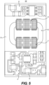
- substrate
- conductive pattern
- terminal
- magnetic core
- lead frame
- Prior art date
- Legal status (The legal status is an assumption and is not a legal conclusion. Google has not performed a legal analysis and makes no representation as to the accuracy of the status listed.)
- Pending
Links
Images











Classifications
-
- H—ELECTRICITY
- H01—ELECTRIC ELEMENTS
- H01F—MAGNETS; INDUCTANCES; TRANSFORMERS; SELECTION OF MATERIALS FOR THEIR MAGNETIC PROPERTIES
- H01F27/00—Details of transformers or inductances, in general
- H01F27/28—Coils; Windings; Conductive connections
- H01F27/30—Fastening or clamping coils, windings, or parts thereof together; Fastening or mounting coils or windings on core, casing, or other support
- H01F27/306—Fastening or mounting coils or windings on core, casing or other support
-
- H—ELECTRICITY
- H01—ELECTRIC ELEMENTS
- H01F—MAGNETS; INDUCTANCES; TRANSFORMERS; SELECTION OF MATERIALS FOR THEIR MAGNETIC PROPERTIES
- H01F27/00—Details of transformers or inductances, in general
- H01F27/28—Coils; Windings; Conductive connections
- H01F27/2804—Printed windings
-
- H—ELECTRICITY
- H01—ELECTRIC ELEMENTS
- H01F—MAGNETS; INDUCTANCES; TRANSFORMERS; SELECTION OF MATERIALS FOR THEIR MAGNETIC PROPERTIES
- H01F27/00—Details of transformers or inductances, in general
- H01F27/28—Coils; Windings; Conductive connections
- H01F27/2895—Windings disposed upon ring cores
-
- H—ELECTRICITY
- H01—ELECTRIC ELEMENTS
- H01F—MAGNETS; INDUCTANCES; TRANSFORMERS; SELECTION OF MATERIALS FOR THEIR MAGNETIC PROPERTIES
- H01F27/00—Details of transformers or inductances, in general
- H01F27/06—Mounting, supporting or suspending transformers, reactors or choke coils not being of the signal type
-
- H—ELECTRICITY
- H01—ELECTRIC ELEMENTS
- H01F—MAGNETS; INDUCTANCES; TRANSFORMERS; SELECTION OF MATERIALS FOR THEIR MAGNETIC PROPERTIES
- H01F27/00—Details of transformers or inductances, in general
- H01F27/24—Magnetic cores
- H01F27/26—Fastening parts of the core together; Fastening or mounting the core on casing or support
- H01F27/266—Fastening or mounting the core on casing or support
-
- H—ELECTRICITY
- H01—ELECTRIC ELEMENTS
- H01F—MAGNETS; INDUCTANCES; TRANSFORMERS; SELECTION OF MATERIALS FOR THEIR MAGNETIC PROPERTIES
- H01F27/00—Details of transformers or inductances, in general
- H01F27/28—Coils; Windings; Conductive connections
- H01F27/29—Terminals; Tapping arrangements for signal inductances
-
- H—ELECTRICITY
- H01—ELECTRIC ELEMENTS
- H01F—MAGNETS; INDUCTANCES; TRANSFORMERS; SELECTION OF MATERIALS FOR THEIR MAGNETIC PROPERTIES
- H01F27/00—Details of transformers or inductances, in general
- H01F27/28—Coils; Windings; Conductive connections
- H01F27/29—Terminals; Tapping arrangements for signal inductances
- H01F27/292—Surface mounted devices
-
- H—ELECTRICITY
- H01—ELECTRIC ELEMENTS
- H01F—MAGNETS; INDUCTANCES; TRANSFORMERS; SELECTION OF MATERIALS FOR THEIR MAGNETIC PROPERTIES
- H01F27/00—Details of transformers or inductances, in general
- H01F27/28—Coils; Windings; Conductive connections
- H01F27/32—Insulating of coils, windings, or parts thereof
- H01F27/324—Insulation between coil and core, between different winding sections, around the coil; Other insulation structures
-
- H—ELECTRICITY
- H01—ELECTRIC ELEMENTS
- H01F—MAGNETS; INDUCTANCES; TRANSFORMERS; SELECTION OF MATERIALS FOR THEIR MAGNETIC PROPERTIES
- H01F5/00—Coils
- H01F5/04—Arrangements of electric connections to coils, e.g. leads
-
- H—ELECTRICITY
- H05—ELECTRIC TECHNIQUES NOT OTHERWISE PROVIDED FOR
- H05K—PRINTED CIRCUITS; CASINGS OR CONSTRUCTIONAL DETAILS OF ELECTRIC APPARATUS; MANUFACTURE OF ASSEMBLAGES OF ELECTRICAL COMPONENTS
- H05K1/00—Printed circuits
- H05K1/18—Printed circuits structurally associated with non-printed electric components
- H05K1/181—Printed circuits structurally associated with non-printed electric components associated with surface mounted components
-
- H—ELECTRICITY
- H01—ELECTRIC ELEMENTS
- H01F—MAGNETS; INDUCTANCES; TRANSFORMERS; SELECTION OF MATERIALS FOR THEIR MAGNETIC PROPERTIES
- H01F5/00—Coils
- H01F5/04—Arrangements of electric connections to coils, e.g. leads
- H01F2005/043—Arrangements of electric connections to coils, e.g. leads having multiple pin terminals, e.g. arranged in two parallel lines at both sides of the coil
-
- H—ELECTRICITY
- H01—ELECTRIC ELEMENTS
- H01F—MAGNETS; INDUCTANCES; TRANSFORMERS; SELECTION OF MATERIALS FOR THEIR MAGNETIC PROPERTIES
- H01F5/00—Coils
- H01F5/04—Arrangements of electric connections to coils, e.g. leads
- H01F2005/046—Details of formers and pin terminals related to mounting on printed circuits
-
- H—ELECTRICITY
- H01—ELECTRIC ELEMENTS
- H01F—MAGNETS; INDUCTANCES; TRANSFORMERS; SELECTION OF MATERIALS FOR THEIR MAGNETIC PROPERTIES
- H01F27/00—Details of transformers or inductances, in general
- H01F27/06—Mounting, supporting or suspending transformers, reactors or choke coils not being of the signal type
- H01F2027/065—Mounting on printed circuit boards
-
- H—ELECTRICITY
- H01—ELECTRIC ELEMENTS
- H01F—MAGNETS; INDUCTANCES; TRANSFORMERS; SELECTION OF MATERIALS FOR THEIR MAGNETIC PROPERTIES
- H01F27/00—Details of transformers or inductances, in general
- H01F27/28—Coils; Windings; Conductive connections
- H01F27/2804—Printed windings
- H01F2027/2809—Printed windings on stacked layers
-
- H—ELECTRICITY
- H01—ELECTRIC ELEMENTS
- H01F—MAGNETS; INDUCTANCES; TRANSFORMERS; SELECTION OF MATERIALS FOR THEIR MAGNETIC PROPERTIES
- H01F27/00—Details of transformers or inductances, in general
- H01F27/28—Coils; Windings; Conductive connections
- H01F27/2804—Printed windings
- H01F2027/2814—Printed windings with only part of the coil or of the winding in the printed circuit board, e.g. the remaining coil or winding sections can be made of wires or sheets
Definitions
- the block coil can include additional first terminals and additional second terminals; the first terminal and the additional first terminals can define a first terminal group; and the second terminal and the additional second terminals can define a second terminal group.
- Each terminal in the first terminal group can be connected to a corresponding primary conductive pattern; and each terminal in the second terminal group can be connected to a corresponding secondary conductive pattern.
- the first terminal group can be located next to and spaced away from the second terminal group.
- the conductive pattern can be a primary conductive pattern, and the first terminal of the first block coil can be connected only to the primary conductive pattern.
- the conductive pattern can be a secondary conductive pattern, and the first terminal of the second block coil can be connected only to the secondary conductive pattern.
- the electronic module can further include a third block coil including first and second terminals, wherein the first terminal can be connected to a primary conductive pattern and wherein the second terminal can be connected to a secondary conductive pattern.
- the first block coil can include a first terminal group and a second terminal group, and the first terminal can be included in the first terminal group.
- Each terminal in the first terminal group can be connected to a corresponding primary conductive pattern
- each terminal in the second terminal group can be connected to a corresponding secondary conductive pattern.
- Each terminal in the first terminal group and each terminal in the second terminal group can be connected to a corresponding primary conductive pattern.
- Each terminal in the first terminal group and each terminal in the second terminal group can be connected to a corresponding secondary conductive pattern.
- the first group can be located next to and spaced away from the second group.
- the substrate or the lead frame can include first and second layers.
- the electronic module can further include a primary conductive pattern in the first layer and a secondary conductive pattern in the second layer, wherein from a side view of the substrate, a portion of the primary conductive pattern and a portion of the secondary conductive pattern can overlap vertically.
- the electronic module can further include an additional primary conductive pattern in a third layer of the substrate and an additional secondary conductive pattern in a fourth layer of the substrate, wherein from the side view of the substrate, a portion of the additional primary conductive pattern and a portion of the additional secondary conductive pattern can overlap vertically.
- the electronic component can include an integrated circuit (IC) and/or a capacitor.
- the electronic module can further include a space between the magnetic core and the substrate or the lead frame where the block coil extends over the magnetic core.
- the material can include a standoff, a standoff pip, an insulative ball, or an insulating shim.
- a magnetic component includes a substrate or a lead frame including a primary conductive pattern and a secondary conductive pattern; a magnetic core located on or above of the substrate or the lead frame; a material located between the magnetic core and either the substrate or the lead frame; a block coil including a resin body that is located on or above the substrate or the lead frame and that extends over the magnetic core, a first terminal that is on or embedded in the resin body and that is connected to the primary conductive pattern, and a second terminal on or embedded in the resin body and that is connected to the secondary conductive pattern; and an insulating material covering the substrate or the lead frame, the magnetic core, and the block coil.
- the magnetic core can be located on the substrate or the lead frame.
- the magnetic core can be located above of the substrate or the lead frame and can be attached to an inner, upper surface of the block coil.
- the magnetic component can further include a coating covering the magnetic core.
- the block coil can include additional first terminals and additional second terminals; the first terminal and the additional first terminals can define a first terminal group; and the second terminal and the additional second terminals can define a second terminal group.
- Each terminal in the first terminal group can be connected to a corresponding primary conductive pattern, and each terminal in the second terminal group can be connected to a corresponding secondary conductive pattern.
- the first terminal group can be located next to and spaced away from the second terminal group.
- the substrate or the lead frame can include first and second layers; the primary conductive pattern can be in the first layer; the secondary conductive pattern can be in the second layer; and from a side view of the substrate or lead frame, a portion of the primary conductive pattern and a portion of the secondary conductive pattern can overlap vertically.
- the magnetic component can further include an additional primary conductive pattern in a third layer of the substrate or the lead frame and an additional secondary conductive pattern in a fourth layer of the substrate or the lead frame, wherein from the side view of the substrate or the lead frame, a portion of the additional primary conductive pattern and a portion of the additional secondary conductive pattern can overlap vertically.
- the material can include a standoff, a standoff pip, an insulative ball, or an insulating shim.
- a magnetic component including a substrate or a lead frame including a first layer, and a conductive pattern; a magnetic core located on or above the substrate or the lead frame; a material located between the magnetic core and either the substrate or the lead frame; first and second block coils, each of the first and the second block coils including a resin body that is located on or above the substrate or the lead frame and that extends over the magnetic core and a first terminal that is on or embedded in the resin body and that is connected to the conductive pattern; and an insulating material covering the substrate or the lead frame, the magnetic core, and the block coil.
- the magnetic core can be located on the substrate or the lead frame.
- the magnetic core can be located above the substrate or the lead frame and can be attached to an inner, upper surface of the first block coil and/or the second block coil.
- the magnetic component can further include a coating covering the magnetic core.
- the magnetic component can further include a primary conductive pattern and a secondary conductive pattern, wherein the first terminal of the first block coil can be connected only to the primary conductive pattern and wherein the first terminal of the second block coil can be connected only to the secondary conductive pattern.
- the magnetic component can further include a third block coil including first and second terminals, wherein the first terminal can be connected to a primary conductive pattern and wherein the second terminal can be connected to a secondary conductive pattern.
- the first block coil can include a first terminal group and a second terminal group; the first terminal can be included in the first terminal group; each terminal in the first terminal group can be connected to a corresponding primary conductive pattern; and each terminal in the second terminal group can be connected to a corresponding secondary conductive pattern.
- the first group can be located next to and spaced away from the second group.
- the magnetic component can further include a primary conductive pattern in the first layer and a secondary conductive pattern in a second layer of the substrate or the lead frame, wherein from a side view of the substrate or the lead frame, a portion of the primary conductive pattern and a portion of the secondary conductive pattern can overlap vertically.
- the magnetic component can further include an additional primary conductive pattern in a third layer of the substrate or the lead frame and an additional secondary conductive pattern in a fourth layer of the substrate or the lead frame, wherein from the side view of the substrate, a portion of the additional primary conductive pattern and a portion of the additional secondary conductive pattern can overlap vertically.
- the material can include a standoff, a standoff pip, an insulative ball, or an insulating shim.
- an electronic module includes a substrate or a lead frame including primary conductive patterns and secondary conductive patterns; a magnetic core located on or above of the substrate or the lead frame; a material located between the magnetic core and either the substrate or the lead frame; a block coil including a resin body that is located on or above the substrate or the lead frame and that extends over the magnetic core, first terminals that define a first terminal group and that are on or embedded in the resin body, and second terminals that define a second terminal group and that on or are embedded in the resin body; an IC located on the substrate or the lead frame; and a capacitor located on the substrate or the lead frame.
- Two first terminals of the first terminal group are connected to corresponding primary conductive patterns; two second terminals of the second terminal group are connected corresponding secondary conductive patterns; and a first primary conductive pattern is closer to a second primary conductive pattern than any of the secondary conductive patterns.
- Each first terminal in the first terminal group can be connected to a corresponding primary conductive pattern, and each second terminal in the second terminal group can be connected to a corresponding secondary conductive pattern.
- the first terminal group can be located next to and spaced away from the second terminal group.
- the substrate or the lead frame can include first and second layers.
- the primary conductive patterns can be in the first layer; the secondary conductive patterns can be in the second layer; and from a side view of the substrate, portions of the primary conductive patterns can overlap vertically corresponding portions of the secondary conductive patterns.
- the electronic module can further include additional primary conductive patterns in a third layer of the substrate and additional secondary conductive patterns in a fourth layer of the substrate, wherein from the side view of the substrate, portions of the additional primary conductive patterns can overlap vertically corresponding portions of the additional secondary conductive pattern.
- the electronic module can further include an insulating material covering the substrate or the lead frame, the magnetic core, and the block coil.
- the electronic module can include the substrate, and the substrate can include a via hole.
- the magnetic core can be located on or above a first surface of the substrate or the lead frame, and the capacitor can be located on a second surface of the substrate or the lead frame opposite to the first surface.
- the electronic module can further include a coating covering the magnetic core.
- the material can include a standoff, a standoff pip, an insulative ball, or an insulating shim.
- an electronic module includes a substrate or a lead frame including primary conductive patterns and secondary conductive patterns; a magnetic core located on or above of the substrate or the lead frame; a material located between the magnetic core and either the substrate or the lead frame; first and second block coils, each of the first and the second block coils includes a resin body that is located on or above the substrate or the lead frame and that extends over the magnetic core, first terminals that define a first terminal group and that are on or embedded in the resin body, and second terminals that define a second terminal group and that are on or embedded in the resin body; an IC located on the substrate or the lead frame; and a capacitor located on the substrate or the lead frame.
- the electronic module can further include an insulating material covering the substrate or the lead frame, the magnetic core, and the block coil.
- the electronic module can include the substrate, and the substrate can include a via hole.
- the magnetic core can be located on or above a first surface of the substrate or the lead frame, and the capacitor can be located on a second surface of the substrate or the lead frame opposite to the first surface.
- the electronic module can further include a coating covering the magnetic core.
- the material can include a standoff, a standoff pip, an insulative ball, or an insulating shim.
- Figs. 1 and 2 show a magnetic component 100 that includes a substrate 20, a magnetic core 30, and two block coils 10.
- Figs. 3-5 show an electronic module 200 that includes the magnetic component 100 of Fig. 1 and additional electronic component(s) 50.
- two block coils 10 are shown in Fig. 1-5 , any number of block coils 10 can be used, including a single block coil 10.
- the substrate 20 can be any suitable substrate, including, for example, a printed circuit board (PCB).
- the substrate 20 can include a single layer or multiple layers and can include traces or conductive patterns 23 on an exterior surface (i.e., the top and the bottom surfaces) of the substrate 20 and/or in the substrate 20 (i.e., on an internal layer of the substrate 20). If the substrate 20 includes a single layer, then the traces or conductive patterns 23 of both the primary winding and the secondary winding can be located on the same layer, e.g., the top surface of the substrate 20. If the substrate 20 includes multiple layers, then the traces or conductive patterns 23 of the primary winding and the secondary winding can be located on the same layer or can be located on different layers.
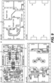
- Fig. 9 shows four possible layers of the substrate 20. Although four layers are shown in Fig. 9 , any number of layers can be used, including one layer.
- Figs. 1 and 2 no additional electronic components 50 are shown on the substrate 20, but as shown for the electronic module 200 of Figs. 3 and 5 , additional electronic component(s) 50 can be included on the substrate 20.
- the electronic component(s) 50 can be active components, such as transistors, integrated circuits (ICs), etc., or can be passive components, such as resistors, capacitors, inductors, etc.
- the electronic component(s) 50 can be connected to the same surface as the magnetic core 30 as shown in Figs. 3 and 5 and/or can be connected to the opposite surface as the magnetic core 30 (not shown). For example, locating capacitors on a surface of the substrate 20 opposite to the magnetic core 30 can contribute to (i) the "miniaturization" of electronic module 200 and (ii) prevent or greatly reduce short circuiting.
- the electronic module 200 can be, for example, a power converter, isolator, or transformer, and the electronic components 50 can be the components of the power converter, isolator, or transformer.
- the electronic module 200 can be any suitable power converter, including, for example, a DC-DC converter or an AC-DC converter.
- a DC-DC converter or an AC-DC converter.
- the electronic module 200 is an isolated DC-DC converter, then, as shown in Figs. 3 and 5 , electronic components 50 of a primary circuit 21 located on a first side of an isolation barrier can be located at one end of the substate, and electronic components 50 of a secondary circuit 22 located on a second side of the isolation barrier can be located at the opposite end of the substrate 20.
- Fig. 16 shows a similar magnetic component 100 as Figs. 1 and 2 , but the substrate 20 in Fig. 16 includes a single-layer substrate.
- the primary traces 23 and the secondary traces 23 can be separated by one or more layers.
- the primary traces 23 and the secondary traces 23 are separated by the 2 nd layer of the substrate 20.
- the primary traces 23 and the secondary traces 23 are separated by three thin film layers for a total separation of 0.15 mm.
- the hatched areas in Fig. 9 are keep-out areas, but other keep-out area arrangements are also possible.
- the area on the 1 st layer between the feet 12 of the terminals 11 of the block coils 10 can also be a keep-out area, which as shown in Fig. 10 includes a keep-out area with a minimum width of 0.4 mm between the block coils 10.
- one or more terminals 11 of each block coils 10 can be connected to a trace 23.
- a single secondary trace 23 can connect a foot of one secondary terminal 11 to a foot of another secondary terminal 11 to define a single turn of the secondary winding
- a primary trace 23 can connect the feet 12 of three primary terminals 11 to the feet 12 of three other primary terminals 11 to define a single turn of the primary winding. That is, it is possible for a single turn of a winding to include one or more terminals 11 connected by a single trace 23.
- FIG. 17 shows a possible circuit arrangement of an electronic module 200 including either (a) a single-layer substrate 20 or (b) a multi-layer substrate 20 in which the electronic component(s) 50 and all of the traces 23 are on the top surface of the substrate 20.
- one or more terminals 11 of each block coil 10 can be connected to a trace 23.
- the traces 23 on the substrate 20 can determine how many terminals 11 are included in a single turn and can determine how many turns are in either the primary or the secondary winding.
- the same block coil 10 can be used in different applications, which can save design costs because a different block coil 10 does not have to be made for each application.
- Fig. 32 shows an example in which a standoff 33 is used to offset the magnetic core 30 from the substrate 20.
- the standoff 33 can be attached to the substrate 20 and then the magnetic core 30 can be attached to the standoff 33.
- the standoff 33 can be attached to the magnetic core 30 and then the standoff 33 can be attached to the substrate 20.
- the standoff 33 can be unitary with the magnetic core 30, in which case the standoff 33 can be attached to the substrate 20.
- an adhesive 34 can be used to attach the standoff 33 to the substrate 20.
- the adhesive 34 may be omitted. Any suitable adhesive can be used, including, for example, a surface mount adhesive (SMA).
- SMA surface mount adhesive
- the standoff 33 can have a sausage shape or any other suitable shape.
- the standoff 33 can have a shape similar to the magnetic core 30 such that the standoff 33 extends along the entire bottom surface of the magnetic core 30.
- the standoff 33 can be made of any suitable material, which can be conductive or non-conductive.
- Figs. 33 and 34 show an example in which a standoff pip 35 is used to offset the magnetic core 30 from the substrate 20.
- the standoff pip 35 is different from the standoff 33 in that the standoff pip 35 penetrates a portion of the magnetic core 30.
- the standoff pip 35 can be attached to the substrate 20 and then the magnetic core 30 can be attached to the standoff pip 35.
- the standoff pip 35 can be attached to the magnetic core 30 and then the standoff pip 35 can be attached to the substrate 20.
- An adhesive (not shown) can be used to attach the standoff pip 35 to the substrate 20.
- Figs. 33 and 34 show four standoff pips 35, any number of standoff pips can be used.
- the standoff pip 35 can have a circular cross section or any other cross-sectional shape.
- the standoff pip 35 can have a shape similar to the magnetic core 30 such that the standoff pip 35 extends along the entire bottom surface of the magnetic core 30.
- the standoff pip 35 can be made of any suitable material, which can be conductive or non-conductive.
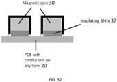
- Figs. 37 shows an example in which an insulative shim 37 is used to offset the magnetic core 30 from the substrate 20.
- the insulative shim 37 can be attached to the substrate 20 and then the magnetic core 30 can be attached to the insulative shim 37.
- the insulative shim 37 can be attached to the magnetic core 30 and then the insulative shim 37 can be attached to the substrate 20.
- An adhesive (not shown) can be used to attach the insulative shim 37 to the substrate 20.
- Fig. 37 shows two insulative shims 37, any number of insulative shims can be used.
- the insulative shim 37 can have a rectangular cross section or any other cross-sectional shape.
- the insulative shim 37 can have a shape similar to the magnetic core 30 such that the insulative shim 37 extends along the entire bottom surface of the magnetic core 30.
- the insulative shim 37 can be made of any suitable insulative material.
- the block coil 10 can include a resin body 17 and terminals 11.
- the resin body 17 can include two legs 13 connected by a bridge 14 to define a cavity or groove 16 that receives a portion of the magnetic core 30.
- the resin body 17 can have a U-shape as shown in Fig. 6 and 7 or can have any suitable shape such that the resin body 17 extends over or bridges the magnetic core 30.
- the resin body 17 can extend over three sides of a cross section of the magnetic core 30.
- the resin body 17 can include slots 15 in which the terminals 11 can be located or embedded in and can define a flat pick-up surface that a pick- and-place machine can use to precisely place the block coil 10 on a substrate 20 in one motion.
- the block coil 10 provides a structure that protects the terminals 11 and prevents or greatly reduces any chance of short-circuiting. Because the resin body 17 allows different arrangements of terminals 11 to be used with the same resin body 17, the same resin body 17 can be used in different applications, which can save design costs because a different resin body 17 does not have to be made for each application. For example, if the resin body 17 is made by a molding process, then the same mold can be used for different applications, saving design costs. In Figs. 6 and 7 , the slots 15 in the resin body 17 are visible, but in the finished product, the slots 15 may not be visible, for example, if a resin mold is used that fills the gaps in the slots 15.
- Fig. 6 shows twelve terminals 11 and four empty slots 15. Any number of terminals 11 can be used, including, for example, 14, 16, 18, 20, or more than 20 terminals.
- the terminals 11 can have a U-shape as shown in Fig. 6 and 7 or can have any suitable shape such that the terminals 11 extend over or bridge the magnetic core 30.
- the terminals 11 can extend over three sides of a cross section of the magnetic core 30.
- the terminals 11 can include feet 12 that can be surface mounted to the substrate 20. Alternatively, the terminals 11 can be connected to the substrate 20 in any suitable manner.
- the feet 12 of the terminals 11 can be attached to the substrate 20 such that the block coil 10, including the resin body 17, is located on or above the substrate 20.
- the terminals 11 can be located or embedded in slots 15 in the block coil 10.
- Fig. 6 shows sixteen slots 15, but any number of slots 15 could be used.
- the terminals 11 in the block coil 10, along with traces 23 on or in the substrate 20, can be included in the windings of the magnetic component 100. If the windings include primary windings and secondary windings, then some terminals 11 can be included in the primary winding and be connected to primary traces 23, and some terminals 11 can be included in the secondary winding and be connected to secondary traces 23. Alternatively, all of the terminals 11 in the block coil 10 either can be included in the primary winding and be connected to primary traces 23 or can be included in the secondary winding and be connected to secondary traces 23. If all of the terminals 11 in one block coil 10 are included in the primary winding, then all of the terminals 11 in another block coil 10 can be included in the secondary winding, and vice versa. If all of the terminals 11 in one block coil 10 are included in the primary winding, then another block can include terminals 11 in both the primary winding and the secondary winding, and vice versa.
- the terminals 11 in a block coil 10 can be included in groups. Which terminal group each terminal 11 belongs to is determined by the traces 23 on the substrate 20. For example, with one substrate 20, all of the terminals 11 might belong to a first terminal group, while with another substrate 20, the adjacent terminals 11 might be in two different terminal groups, either a first terminal group or a second terminal group.
- Fig. 6 shows two terminal groups, i.e., first and second terminal groups.
- the first terminal group includes four first terminals 11 on each end of the block coil 10
- the second terminal group includes four second terminals 11 in the middle of the block coil 10 in between the first terminals 11 of the first terminal group.
- Other arrangements are also possible.
- the first and second terminals 11 can alternate along the length of the block coil 10 such that each terminal 11 of one terminal group can be between two terminals 11 of the other terminal group.
- the terminal groups do not have to be split. That is, the terminals 11 of the first terminal group can be located on one end of the block coil 10 (e.g., seven first terminals 11 on one end), and the terminals 11 of the second terminal group can be located on the other end of the block coil 10 (e.g., seven second terminals 11 on the other end with two slots 15 in the middle without any terminals 11).
- the terminals 11 can also be arranged in a bifilar arrangement in which two windings are arranged next to each other. For example, adjacent terminals 11 can be connected to either a first primary winding or a second primary winding.
- Each terminal 11 of the first or the second terminal group can be closer to an adjacent terminal 11 of the same group than a terminal 11 of the other group. That is, each first terminal 11 can be closer to another first terminal 11 than any second terminal 11, and each second terminal 11 can be closer to another second terminal 11 than any first terminal 11.
- Slots 15 between adjacent terminal groups can be empty (i.e., the number of terminals 11 can be reduced or thinned) to help improve isolation between the first and second terminal groups. More empty slots 15 between adjacent terminal groups can increase the isolation between the terminal groups.
- the adjacent terminal groups can be spaced away from each other. Instead of including empty slots 15, adjacent terminal groups can be spaced farther apart from each other than adjacent terminals 11 in a terminal group. For example, adjacent terminal groups can be spaced apart twice the distance that adjacent terminals 11 in a terminal group are spaced part, with no empty slots 15 between the adjacent terminal groups.
- Fig. 8 shows two block coils 10 with terminals 11 with different widths. As shown in Fig. 8 , the terminals 11 of each block coil 10 can have the same width. Alternatively, the terminals 11 with different widths can be included in the same block coil 10.
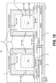
- Fig. 10 shows the cross-section of two block coils 10 connected to a multi-layer substrate 20.
- Fig. 10 shows various minimum distances that ensure adequate isolation.
- the walls of the resin body 17 should be at least 0.4 mm thick so that the terminals 11 are at least 0.4 mm from the cavity or groove 16 within the block coil 10. If the magnetic core 30 is coated, then 0.4 mm wall thickness can be reduced, for example, to 0.2 mm.
- the isolation distance will depend on the application.
- the minimum distance between the magnetic core 30 and the walls of the resin body 17 can be 0.0 mm so that there is no distance between the magnetic core 30 and the walls of the resin body 17.
- the minimum distance between the traces or conductive patterns 23 of the primary and secondary circuits should be at least 0.4 mm.
- the substrate 20 can include laser vias that can be created by laser and that do not have to extend all the way through the substrate 20 and can include buried vias that extend between internal layers of the substrate 20 but that do not extend the external surfaces of the substrate 20.
- Each of the multiple layers of the substrate 20 can be 0.05 mm or approximately 0.05 mm within manufacturing and/or measurement tolerances.
- the primary traces 23 and the secondary traces 23 can be separated by three internal layers such that the total distance between the primary traces 23 and the secondary traces 23 is at least 0.15 mm to ensure adequate isolation.
- distance 1 is the thickness of the walls of the block coil 10 and can be about 0.01 mm to about 2.0 mm, within manufacturing and/or measurement tolerances
- distance 2 is the distance between the trace 23 on the top layer of the substrate 20 and the magnetic core 30 and can be about 0.01 mm to about 2.0 mm, within manufacturing and/or measurement tolerances
- distance 3 is the smallest distance between the between the block coils 10 (which is the distance between the feet 12 of the terminals 11 in Fig. 18 ) and can be about 0.01 mm to about 2.0 mm, within manufacturing and/or measurement tolerances.
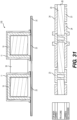
- Figs. 26-31 show different possible substrates 20 that can be used in either a magnetic component 100 or in an electronic module 200.
- Figs. 26-30 show different possible multi-layer substrates 20, while Fig. 31 shows a single-layer substrate 20.
- the substrate 20 can include multiple layers, including a top mask 24, one or more pre-preg layers 27, a core layer 28, one or more pre-preg layers 27, and a bottom mask 24.
- the core layer 28 can also include a core pre-preg layer 28a.
- the core layer 28 can include any suitable material, including, for example, FR-4. Traces 23 can be included on the top and bottom surfaces of the substrate 20 and can be included in interior layers of the substrate 20.
- the traces 23 on different layers can be connected by vias.
- the vias can include a hole in the substrate 20 that is plated with a conductive material, including, for example, a metal or metal alloy, and filled with any suitable material, including, for example, a resin. Alternatively, the vias can be filled with only conductive material.
- the vias can be made in any suitable manner, including, for example, mechanical drilling or laser drilling. Any suitable vias can be used, including, buried vias in which neither side of the vias is exposed on the top or bottom surface of the substrate 20, blind vias in which one side of the vias is exposed on the top or bottom surface of the substrate 20, and through-hole vias in which both sides of the vias are exposed on either the top or the bottom surface of the substrate 20.
- the traces 23 can include copper or other suitable conductive material.
- the substrate 20 can include a single layer, including a a top mask 24, a core layer 28, and a bottom mask 24.
- the traces 23 in Fig. 31 can be located on the top or the bottom surfaces of the substrate 20.
- Fig. 26 shows a multi-layer substrate 20 that includes a top mask 24, a pre-preg layer 27, a core pre-preg layer 28a, a core layer 28, two pre-preg layers 27, and a bottom mask 24. Traces 23 are located on the top and bottom surfaces of the substrate 20, the top surface of the core pre-preg layer 28a, and the bottom surface of the core layer 28.
- Fig. 27 shows a multi-layer substrate 20 that includes a top mask 24, a pre-preg layer 27, a core pre-preg layer 28a, a core layer 28, three pre-preg layers 27, and a bottom mask 24.
- Traces 23 are located on the top and bottom surfaces of the substrate 20, the top surface of the core pre-preg layer 28a, and the bottom surface of the core layer 28.
- Fig. 28 shows a multi-layer substrate 20 that includes a top mask 24, a pre-preg layer 27, a core layer 28, three pre-preg layers 27, and a bottom mask 24. Traces 23 are located on the top and bottom surfaces of the substrate 20 and the top and bottom surfaces of the core layer 28.
- Fig. 29 shows a multi-layer substrate 20 that includes a top mask 24, a pre-preg layer 27, a core layer 28, a pre-preg layer 27, and a bottom mask 24. Traces 23 are located on the top and bottom surfaces of the substrate 20 and the top and bottom surfaces of the core layer 28.
- Fig. 30 shows a multi-layer substrate 20 that includes a top mask 24, two pre-preg layers 27, a core layer 28, two pre-preg layers 27, and a bottom mask 24. Traces 23 are located on the top and bottom surfaces of the substrate 20 and the top and bottom surfaces of the core layer 28.
- the multi-layer substrate in Figs. 26-30 makes it easier to locate the primary and the secondary traces or conductive patterns 23 and to provide insulation between the primary and the secondary traces or conductive patterns 23. If multiple block coils 10 are used, then the multi-layer substrate in Figs. 26-30 can make it easier to provide isolation between the primary and the secondary traces or conductive patterns 23.
- the bottom portion of Fig. 31 shows a single-layer substrate 20 that includes a top mask 24, a core layer 28, and a bottom mask 24. Traces 23 are located on the top and bottom surfaces of the substrate 20.
- the top portion of Fig. 31 shows a magnetic component 100 including two block coils 10 mounted to the single-layer substrate 20 and including a magnetic core 30. The traces 23 are on the top surface of the single-layer substrate 50.
- the single-layer substrate 20 allows for a smaller magnetic component 100 or electronic module 200.
- one of the block coils 10 can include primary terminals 11 and the other block coils 10 can include secondary terminals 11 so that primary traces 23 connected to the primary terminals 11 and the secondary traces 23 connected to the secondary terminals can be located on the same surface of the substrate 10.
- portions of the secondary traces 23 and the primary traces 23 can overlap vertically, which can improve coupling between the primary and the secondary windings.
- the resistance can be lowered if primary traces 23 or if the secondary traces 23 are located on adjacent layers. That is, the resistance can be lowered in the primary winding if primary traces 23 on different layers are only separated by a single layer, and the resistance can be lowered in the secondary winding if secondary traces 23 on different layers are only separated by a single layer.
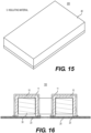
- Figs. 11-15 show a method of making an electronic module 200 with block coils 10 mounted to a substrate 20.
- Fig. 11 shows providing a substrate 20 and then applying solder paste 25.
- the substrate 20 can be one of the substrates 20 discussed above and can be multi-layer or single-layer substrate.
- Fig. 12 shows glue or adhesive 26 being dispensed on the substrate 20.
- the glue or adhesive 26 can be dispensed as part of a surface mount technology (SMT) process or separate from an SMT process.
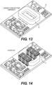
- Fig. 13 shows the placement of the magnetic core 30 and the electronic component(s) 50.
- Fig. 14 shows the placement of two block coils 10 that extend over or bridge the magnetic core 30.
- insulating material 40 covering the substrate 20, the electronic component(s) 50, the magnetic core 30, and the block coils 10.
- Fig. 15 shows that the insulating material 40 covers the entire substrate 20, but the insulating material 40 can cover only a portion of the substrate 40 and/or cover only one or some of the electronic component(s) 50, the magnetic core 30, and the block coils 10.
- a mother substrate can be used in which an array of electronic modules 200 are included in the mother substrate. The mother substrate is then diced or singulated to form individual electronic modules 200.
- individual electronic module 200 can be manufactured without using a mother substrate.
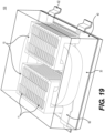
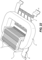
- Figs. 19-23 show a magnetic component 100 similar to the magnetic component 100 of Fig. 1 .
- the magnetic component 100 can include the block coils 10 and the magnetic core 30 of the magnetic component 100 of Fig. 1 .
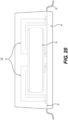
- the magnetic component 100 of Figs. 19-23 is different from the magnetic component 100 of Fig. 1 in that the block coils 10 of the magnetic component 100 of Figs. 19-23 are connected to a lead frame 60 instead of a substrate 20.
- the magnetic component 100 of Figs. 19-23 includes an insulating material 40, which is similar to the insulating material 40 applied to the electronic module 200 of Fig. 4 .
- the insulating material 40 is shown as transparent, but in Fig. 23 , the insulating material 40 is shown as not being transparent.
- Fig. 22 does not show the insulating material 40 and one of the block coils 10.
- additional electronic components can be included to form an electronic module 200 so that the magnetic component 100 can be part of, for example, a DC-DC converter.
- the lead frame 60 can include mounting terminals 62 and conductive patterns 61.
- the mounting terminals 62 can be used to connect the lead frame 60, and the magnetic component 100 or electronic module 200, to a host substrate (not shown).
- the conductive patterns 61 are similar to the traces 23 included on or in the substrate 20, and, as similarly described above, the conductive patterns 61 can connect one or more terminals 11 to define a single turn of winding.
- the conductive patterns 61 can determine which winding a terminal 11 is connected to.
- the conductive patterns 61 can be connected to the terminals 11 such that one block coil 10 includes two turns of a primary winding and that the other block coil includes four turns of a secondary winding.
- the terminals 11 in the block coils 10 in the magnetic component 100 of Figs. 19-23 can be separated into different terminal groups as described above with respect to the block coils 10 in the magnetic component 100 of Fig. 1 .
Landscapes
- Engineering & Computer Science (AREA)
- Power Engineering (AREA)
- Microelectronics & Electronic Packaging (AREA)
- Coils Or Transformers For Communication (AREA)
Abstract
An electronic module includes a substrate or a lead frame including a primary conductive pattern and a secondary conductive pattern; a magnetic core located on or above the substrate or the lead frame; a material located between the substrate and the magnetic core; a block coil including a resin body that is located on or above the substrate or the lead frame and that extends over the magnetic core, a first terminal that is on or embedded in the resin body and that is connected to the primary conductive pattern, and a second terminal that is on or embedded in the resin body and that is connected to the secondary conductive pattern; and an electronic component located on the substrate or the lead frame.
Description
- The present invention relates to block coils. More specifically, the present invention relates to block coils that can be attached to a substrate or a lead frame and that can be used in a magnetic component or an electronic module.
- It is known to use windings that include terminals that extend over a magnetic core. Because no structure supports the terminals, there is a risk that the terminals will short circuit or fall sideways.
- To overcome the problems described above, example embodiments of the present invention provide block coils that include a resin body and terminals on or in the resin body such that the risks of the block coil causing a short circuit and the terminals falling are eliminated or greatly reduced.
- According to an example embodiment of the present invention, an electronic module includes a substrate or a lead frame including a primary conductive pattern and a secondary conductive pattern; a magnetic core located on or above the substrate or the lead frame; a material located between the magnetic core and either the substrate or the lead frame; a block coil including a resin body that is located on or above the substrate or the lead frame and that extends over the magnetic core, a first terminal that is on or embedded in the resin body and that is connected to the primary conductive pattern, and a second terminal that is on or embedded in the resin body and that is connected to the secondary conductive pattern; and an electronic component located on the substrate or the lead frame.
- The block coil can include additional first terminals and additional second terminals; the first terminal and the additional first terminals can define a first terminal group; and the second terminal and the additional second terminals can define a second terminal group. Each terminal in the first terminal group can be connected to a corresponding primary conductive pattern; and each terminal in the second terminal group can be connected to a corresponding secondary conductive pattern. The first terminal group can be located next to and spaced away from the second terminal group.
- The substrate or the lead frame can include first and second layers. The primary conductive pattern can be in the first layer; the secondary conductive pattern can be in the second layer; and from a side view of the substrate, a portion of the primary conductive pattern and a portion of the secondary conductive pattern can overlap vertically. The electronic module can further include an additional primary conductive pattern in a third layer of the substrate and an additional secondary conductive pattern in a fourth layer of the substrate, wherein from the side view of the substrate, a portion of the additional primary conductive pattern and a portion of the additional secondary conductive pattern can overlap vertically.
- The electronic module can further include a space between the magnetic core and the substrate or the lead frame where the block coil extends over the magnetic core. The electronic component can include an integrated circuit (IC) and/or a capacitor. The material can include a standoff, a standoff pip, an insulative ball, or an insulating shim.
- According to an example embodiment of the present invention, an electronic module includes a substrate or a lead frame including a conductive pattern; a magnetic core located on or above the substrate or the lead frame; a material located between the substrate and the magnetic core; first and second block coils, each of the first and the second block coils including a resin body that is located on or above the substrate or the lead frame and that extends over the magnetic core and including a first terminal that is on or embedded in the resin body and that is connected to the conductive pattern; an electronic component located on the substrate or the lead frame; and an insulating material covering the substrate or the lead frame, the magnetic core, and the block coil.
- The conductive pattern can be a primary conductive pattern, and the first terminal of the first block coil can be connected only to the primary conductive pattern. The conductive pattern can be a secondary conductive pattern, and the first terminal of the second block coil can be connected only to the secondary conductive pattern. The electronic module can further include a third block coil including first and second terminals, wherein the first terminal can be connected to a primary conductive pattern and wherein the second terminal can be connected to a secondary conductive pattern.
- The first block coil can include a first terminal group and a second terminal group, and the first terminal can be included in the first terminal group. Each terminal in the first terminal group can be connected to a corresponding primary conductive pattern, and each terminal in the second terminal group can be connected to a corresponding secondary conductive pattern. Each terminal in the first terminal group and each terminal in the second terminal group can be connected to a corresponding primary conductive pattern. Each terminal in the first terminal group and each terminal in the second terminal group can be connected to a corresponding secondary conductive pattern. The first group can be located next to and spaced away from the second group.
- The substrate or the lead frame can include first and second layers. The electronic module can further include a primary conductive pattern in the first layer and a secondary conductive pattern in the second layer, wherein from a side view of the substrate, a portion of the primary conductive pattern and a portion of the secondary conductive pattern can overlap vertically. The electronic module can further include an additional primary conductive pattern in a third layer of the substrate and an additional secondary conductive pattern in a fourth layer of the substrate, wherein from the side view of the substrate, a portion of the additional primary conductive pattern and a portion of the additional secondary conductive pattern can overlap vertically.
- The electronic component can include an integrated circuit (IC) and/or a capacitor. The electronic module can further include a space between the magnetic core and the substrate or the lead frame where the block coil extends over the magnetic core. The material can include a standoff, a standoff pip, an insulative ball, or an insulating shim.
- According to an example embodiment of the present invention, a magnetic component includes a substrate or a lead frame including a primary conductive pattern and a secondary conductive pattern; a magnetic core located on or above of the substrate or the lead frame; a material located between the magnetic core and either the substrate or the lead frame; a block coil including a resin body that is located on or above the substrate or the lead frame and that extends over the magnetic core, a first terminal that is on or embedded in the resin body and that is connected to the primary conductive pattern, and a second terminal on or embedded in the resin body and that is connected to the secondary conductive pattern; and an insulating material covering the substrate or the lead frame, the magnetic core, and the block coil.
- The magnetic core can be located on the substrate or the lead frame. The magnetic core can be located above of the substrate or the lead frame and can be attached to an inner, upper surface of the block coil. The magnetic component can further include a coating covering the magnetic core.
- The block coil can include additional first terminals and additional second terminals; the first terminal and the additional first terminals can define a first terminal group; and the second terminal and the additional second terminals can define a second terminal group. Each terminal in the first terminal group can be connected to a corresponding primary conductive pattern, and each terminal in the second terminal group can be connected to a corresponding secondary conductive pattern. The first terminal group can be located next to and spaced away from the second terminal group.
- The substrate or the lead frame can include first and second layers; the primary conductive pattern can be in the first layer; the secondary conductive pattern can be in the second layer; and from a side view of the substrate or lead frame, a portion of the primary conductive pattern and a portion of the secondary conductive pattern can overlap vertically. The magnetic component can further include an additional primary conductive pattern in a third layer of the substrate or the lead frame and an additional secondary conductive pattern in a fourth layer of the substrate or the lead frame, wherein from the side view of the substrate or the lead frame, a portion of the additional primary conductive pattern and a portion of the additional secondary conductive pattern can overlap vertically. The material can include a standoff, a standoff pip, an insulative ball, or an insulating shim.
- According to an example embodiment of the present invention, a magnetic component including a substrate or a lead frame including a first layer, and a conductive pattern; a magnetic core located on or above the substrate or the lead frame; a material located between the magnetic core and either the substrate or the lead frame; first and second block coils, each of the first and the second block coils including a resin body that is located on or above the substrate or the lead frame and that extends over the magnetic core and a first terminal that is on or embedded in the resin body and that is connected to the conductive pattern; and an insulating material covering the substrate or the lead frame, the magnetic core, and the block coil.
- The magnetic core can be located on the substrate or the lead frame. The magnetic core can be located above the substrate or the lead frame and can be attached to an inner, upper surface of the first block coil and/or the second block coil. The magnetic component can further include a coating covering the magnetic core.
- The magnetic component can further include a primary conductive pattern and a secondary conductive pattern, wherein the first terminal of the first block coil can be connected only to the primary conductive pattern and wherein the first terminal of the second block coil can be connected only to the secondary conductive pattern. The magnetic component can further include a third block coil including first and second terminals, wherein the first terminal can be connected to a primary conductive pattern and wherein the second terminal can be connected to a secondary conductive pattern. The first block coil can include a first terminal group and a second terminal group; the first terminal can be included in the first terminal group; each terminal in the first terminal group can be connected to a corresponding primary conductive pattern; and each terminal in the second terminal group can be connected to a corresponding secondary conductive pattern. The first group can be located next to and spaced away from the second group. The magnetic component can further include a primary conductive pattern in the first layer and a secondary conductive pattern in a second layer of the substrate or the lead frame, wherein from a side view of the substrate or the lead frame, a portion of the primary conductive pattern and a portion of the secondary conductive pattern can overlap vertically. The magnetic component can further include an additional primary conductive pattern in a third layer of the substrate or the lead frame and an additional secondary conductive pattern in a fourth layer of the substrate or the lead frame, wherein from the side view of the substrate, a portion of the additional primary conductive pattern and a portion of the additional secondary conductive pattern can overlap vertically. The material can include a standoff, a standoff pip, an insulative ball, or an insulating shim.
- According to an example embodiment of the present invention, an electronic module includes a substrate or a lead frame including primary conductive patterns and secondary conductive patterns; a magnetic core located on or above of the substrate or the lead frame; a material located between the magnetic core and either the substrate or the lead frame; a block coil including a resin body that is located on or above the substrate or the lead frame and that extends over the magnetic core, first terminals that define a first terminal group and that are on or embedded in the resin body, and second terminals that define a second terminal group and that on or are embedded in the resin body; an IC located on the substrate or the lead frame; and a capacitor located on the substrate or the lead frame. Two first terminals of the first terminal group are connected to corresponding primary conductive patterns; two second terminals of the second terminal group are connected corresponding secondary conductive patterns; and a first primary conductive pattern is closer to a second primary conductive pattern than any of the secondary conductive patterns.
- Each first terminal in the first terminal group can be connected to a corresponding primary conductive pattern, and each second terminal in the second terminal group can be connected to a corresponding secondary conductive pattern. The first terminal group can be located next to and spaced away from the second terminal group.
- The substrate or the lead frame can include first and second layers. The primary conductive patterns can be in the first layer; the secondary conductive patterns can be in the second layer; and from a side view of the substrate, portions of the primary conductive patterns can overlap vertically corresponding portions of the secondary conductive patterns. The electronic module can further include additional primary conductive patterns in a third layer of the substrate and additional secondary conductive patterns in a fourth layer of the substrate, wherein from the side view of the substrate, portions of the additional primary conductive patterns can overlap vertically corresponding portions of the additional secondary conductive pattern.
- The electronic module can further include an insulating material covering the substrate or the lead frame, the magnetic core, and the block coil. The electronic module can include the substrate, and the substrate can include a via hole. The magnetic core can be located on or above a first surface of the substrate or the lead frame, and the capacitor can be located on a second surface of the substrate or the lead frame opposite to the first surface. The electronic module can further include a coating covering the magnetic core. The material can include a standoff, a standoff pip, an insulative ball, or an insulating shim.
- According to an example embodiment of the present invention, an electronic module includes a substrate or a lead frame including primary conductive patterns and secondary conductive patterns; a magnetic core located on or above of the substrate or the lead frame; a material located between the magnetic core and either the substrate or the lead frame; first and second block coils, each of the first and the second block coils includes a resin body that is located on or above the substrate or the lead frame and that extends over the magnetic core, first terminals that define a first terminal group and that are on or embedded in the resin body, and second terminals that define a second terminal group and that are on or embedded in the resin body; an IC located on the substrate or the lead frame; and a capacitor located on the substrate or the lead frame. Two first terminals of the first terminal group are connected to corresponding primary conductive patterns; two second terminals of the second terminal group are connected corresponding secondary conductive patterns; and a first primary conductive pattern is closer to a second primary conductive pattern than any of the secondary conductive patterns.
- Each first terminal in the first terminal group can be connected to a corresponding primary conductive pattern, and each second terminal in the second terminal group can be connected to a corresponding secondary conductive pattern. The first terminal group can be located next to and can be spaced away from the second terminal group.
- The substrate or the lead frame can include first and second layers. The primary conductive patterns can be in the first layer; the secondary conductive patterns can be in the second layer; and from a side view of the substrate, portions of the primary conductive patterns can overlap vertically corresponding portions of the secondary conductive patterns. The electronic module can further include additional primary conductive patterns in a third layer of the substrate and additional secondary conductive patterns in a fourth layer of the substrate, wherein from the side view of the substrate, portions of the additional primary conductive patterns can overlap vertically corresponding portions of the additional secondary conductive pattern.
- The electronic module can further include an insulating material covering the substrate or the lead frame, the magnetic core, and the block coil. The electronic module can include the substrate, and the substrate can include a via hole. The magnetic core can be located on or above a first surface of the substrate or the lead frame, and the capacitor can be located on a second surface of the substrate or the lead frame opposite to the first surface. The electronic module can further include a coating covering the magnetic core. The material can include a standoff, a standoff pip, an insulative ball, or an insulating shim.
- The above and other features, elements, characteristics, steps, and advantages of the present invention will become more apparent from the following detailed description of example embodiments of the present invention with reference to the attached drawings.
-
-
Fig. 1 is a top perspective view of block coils mounted to a substrate of a magnetic component. -
Fig. 2 is a top view of the block coils mounted to a PCB of the magnetic component ofFig. 1 . -
Fig. 3 is a top perspective view of block coils mounted to a PCB of the magnetic component ofFig. 1 in an electronic module. -
Fig. 4 is a top perspective view of the electronic module ofFig. 3 with insulating material covering the block coils. -
Fig. 5 is a top view of the electronic module ofFig. 3 . -
Fig. 6 is top perspective view of the block coil ofFig. 1 . -
Fig. 7 is bottom perspective view of the block coil ofFig. 1 . -
Fig. 8 is a top perspective view of block coils with terminals with different widths. -
Fig. 9 shows top views of different layers of the PCB that can be used with the electronic module ofFig. 3 . -
Fig. 10 is a partial sectional view of the electronic module ofFig. 4 with insulating material covering the block coils. -
Figs. 11-15 are perspective views showing a method of manufacturing the electronic module ofFig. 3 . -
Fig. 16 is a sectional view of block coil mounted to a single-layer substrate of an electronic component. -
Fig. 17 is a top view of the top layer of the substrate ofFig. 16 . -
Fig. 18 is a sectional view of a magnetic component showing various distances. -
Fig. 19 is a top perspective view of block coils mounted to lead frame of a magnetic component. -
Fig. 20 is a side sectional view of the block coils mounted to the lead frame of the magnetic component ofFig. 19 . -
Fig. 21 is a bottom perspective view of the block coils mounted to the lead frame of the magnetic component ofFig. 19 . -
Fig. 22 is a top perspective view of a partially assembled magnetic component ofFig. 20 . -
Fig. 23 is a top perspective view of the magnetic component ofFig. 20 with insulating material covering the block coils. -
Fig. 24 shows an E-E or E-I magnetic core that can be used with three block coils. -
Fig. 25 shows a rod-shaped magnetic core that can be used with a single block coil. -
Figs. 26-31 show example substrates that can be used in the magnetic component ofFig. 1 and the electronic module ofFig. 3 . -
Fig. 32 is a sectional view of a magnetic module with material between the magnetic core and substrate. -
Figs. 33 and 34 are a sectional view and a top view of a magnetic module with a magnetic core with standoff pips. -
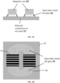
Figs. 35 and 36 are a sectional view and a top view of a magnetic module with glue including glass balls between the magnetic core and the substrate. -
Fig. 37 is a sectional view of a magnetic module with insulating shim between the magnetic core and the substrate. -
Figs. 1 and2 show amagnetic component 100 that includes asubstrate 20, amagnetic core 30, and two block coils 10.Figs. 3-5 show anelectronic module 200 that includes themagnetic component 100 ofFig. 1 and additional electronic component(s) 50. Although twoblock coils 10 are shown inFig. 1-5 , any number of block coils 10 can be used, including asingle block coil 10. - The
magnetic component 100 can include one or more windings that wind around themagnetic core 30. For example, themagnetic component 100 can include a primary winding and a secondary winding that both extend around themagnetic core 30. Each winding can include one ormore terminals 11 in a block coil or block coils 10 and can include one or more traces orconductive patterns 23 on or in thesubstrate 20. - The
substrate 20 can be any suitable substrate, including, for example, a printed circuit board (PCB). Thesubstrate 20 can include a single layer or multiple layers and can include traces orconductive patterns 23 on an exterior surface (i.e., the top and the bottom surfaces) of thesubstrate 20 and/or in the substrate 20 (i.e., on an internal layer of the substrate 20). If thesubstrate 20 includes a single layer, then the traces orconductive patterns 23 of both the primary winding and the secondary winding can be located on the same layer, e.g., the top surface of thesubstrate 20. If thesubstrate 20 includes multiple layers, then the traces orconductive patterns 23 of the primary winding and the secondary winding can be located on the same layer or can be located on different layers.Fig. 9 shows four possible layers of thesubstrate 20. Although four layers are shown inFig. 9 , any number of layers can be used, including one layer. - As shown in
Fig. 3 (inFig. 3 , the insulatingmaterial 40 is shown as transparent) andFig. 4 (inFig. 4 , the insulatingmaterial 40 is not transparent), an insulatingmaterial 40 can be applied to theelectronic module 200 to cover thesubstrate 20, themagnetic core 30, the twoblock coils 10, and any additional electronic component(s) 50. Any suitable insulatingmaterial 40 can be used, including, for example, a molding compound or an epoxy. The insulatingmaterial 40 can be applied in any suitable manner. The insulatingmaterial 40 can improve and help maintain isolation between the primary and the secondary circuit of themagnetic component 100. Insulatingmaterial 40 can also be applied to themagnetic component 100 ofFig. 1 . - In
Figs. 1 and2 , no additionalelectronic components 50 are shown on thesubstrate 20, but as shown for theelectronic module 200 ofFigs. 3 and5 , additional electronic component(s) 50 can be included on thesubstrate 20. The electronic component(s) 50 can be active components, such as transistors, integrated circuits (ICs), etc., or can be passive components, such as resistors, capacitors, inductors, etc. The electronic component(s) 50 can be connected to the same surface as themagnetic core 30 as shown inFigs. 3 and5 and/or can be connected to the opposite surface as the magnetic core 30 (not shown). For example, locating capacitors on a surface of thesubstrate 20 opposite to themagnetic core 30 can contribute to (i) the "miniaturization" ofelectronic module 200 and (ii) prevent or greatly reduce short circuiting. - The
electronic module 200 can be, for example, a power converter, isolator, or transformer, and theelectronic components 50 can be the components of the power converter, isolator, or transformer. Theelectronic module 200 can be any suitable power converter, including, for example, a DC-DC converter or an AC-DC converter. For example, if theelectronic module 200 is an isolated DC-DC converter, then, as shown inFigs. 3 and5 ,electronic components 50 of aprimary circuit 21 located on a first side of an isolation barrier can be located at one end of the substate, andelectronic components 50 of asecondary circuit 22 located on a second side of the isolation barrier can be located at the opposite end of thesubstrate 20. -
Fig. 16 shows a similarmagnetic component 100 asFigs. 1 and2 , but thesubstrate 20 inFig. 16 includes a single-layer substrate. - In
Fig. 9 , the 1st layer of thesubstrate 20 shows the top surface of anelectronic module 200 on which themagnetic core 30 can be located and to which the block coils 10 and theelectronic components 50 can be attached. The 1st layer can include traces orconductive patterns 23 that connect theelectronic components 50. Thetraces 23 of the primary winding (i.e., primary traces or primary conductive patterns) and thetraces 23 of the secondary winding (i.e., secondary traces or secondary conductive patterns) can be located on different layers of thesubstrate 20 as shown inFig. 9 or can be located on the same layer of thesubstrate 20. For example, the primary traces 23 can be located on the 3rd layer of thesubstrate 20, and thesecondary traces 23 can be located on the 1st layer. The primary traces 23 and thesecondary traces 23 can be separated by one or more layers. InFig. 9 , the primary traces 23 and thesecondary traces 23 are separated by the 2nd layer of thesubstrate 20. In the cross-sectional view ofFig. 10 , the primary traces 23 and thesecondary traces 23 are separated by three thin film layers for a total separation of 0.15 mm. The hatched areas inFig. 9 are keep-out areas, but other keep-out area arrangements are also possible. For example, the area on the 1st layer between thefeet 12 of theterminals 11 of the block coils 10 can also be a keep-out area, which as shown inFig. 10 includes a keep-out area with a minimum width of 0.4 mm between the block coils 10. The outer layer of thesubstrate 20 can include input/output (I/O) terminals P1, P2, P3, P4 that can be used to connect theelectronic module 200 to a host substrate (not shown). I/O terminals P1, P2 can be connected to an input voltage, and I/O terminals P3, P4 can provide an output voltage. - As shown in
Fig. 9 , one ormore terminals 11 of each block coils 10 can be connected to atrace 23. For example, in one of the block coils 10, a singlesecondary trace 23 can connect a foot of onesecondary terminal 11 to a foot of anothersecondary terminal 11 to define a single turn of the secondary winding, or in one of the block coils 10, aprimary trace 23 can connect thefeet 12 of threeprimary terminals 11 to thefeet 12 of three otherprimary terminals 11 to define a single turn of the primary winding. That is, it is possible for a single turn of a winding to include one ormore terminals 11 connected by asingle trace 23.Fig. 17 shows a possible circuit arrangement of anelectronic module 200 including either (a) a single-layer substrate 20 or (b) amulti-layer substrate 20 in which the electronic component(s) 50 and all of thetraces 23 are on the top surface of thesubstrate 20. As inFig. 9 , one ormore terminals 11 of eachblock coil 10 can be connected to atrace 23. The traces 23 on thesubstrate 20 can determine howmany terminals 11 are included in a single turn and can determine how many turns are in either the primary or the secondary winding. Thus, thesame block coil 10 can be used in different applications, which can save design costs because adifferent block coil 10 does not have to be made for each application. - The
magnetic core 30 can have any suitable shape including the ring shape shown inFigs. 1-3 and5 or other suitable shapes such as E-I or E-Emagnetic core 31 as shown inFig. 24 , a straight or rod-shapedmagnetic core 32 as shown inFig. 25 , oval-shaped magnetic core (not shown), etc. Themagnetic core magnetic core magnetic core magnetic core substrate 20 or the block coil(s) 10. If themagnetic core magnetic core - The
magnetic core 30 can be offset from thesubstrate 20 such that themagnetic core 30 floats above thesubstrate 20 with a space between themagnetic core 30 and thesubstate 20. Any suitable material or structure can be used to provide the offset between themagnetic core 30 and thesubstrate 20 or to allow themagnetic core 30 to float above thesubstrate 20.Figs. 32-37 show different examples of structures and materials that can be used with asubstrate 20, but similar structures and materials can be used with thelead frame 60 shown inFigs. 19-23 and discussed below. -
Fig. 32 shows an example in which a standoff 33 is used to offset themagnetic core 30 from thesubstrate 20. The standoff 33 can be attached to thesubstrate 20 and then themagnetic core 30 can be attached to the standoff 33. Alternatively, the standoff 33 can be attached to themagnetic core 30 and then the standoff 33 can be attached to thesubstrate 20. Instead of the standoff 33 being separate from themagnetic core 30, the standoff 33 can be unitary with themagnetic core 30, in which case the standoff 33 can be attached to thesubstrate 20. As shown inFig. 32 , an adhesive 34 can be used to attach the standoff 33 to thesubstrate 20. In some applications, the adhesive 34 may be omitted. Any suitable adhesive can be used, including, for example, a surface mount adhesive (SMA). AlthoughFig. 32 shows a single standoff 33, any number of standoffs can be used. The standoff 33 can have a sausage shape or any other suitable shape. For example, the standoff 33 can have a shape similar to themagnetic core 30 such that the standoff 33 extends along the entire bottom surface of themagnetic core 30. The standoff 33 can be made of any suitable material, which can be conductive or non-conductive. -
Figs. 33 and 34 show an example in which astandoff pip 35 is used to offset themagnetic core 30 from thesubstrate 20. Thestandoff pip 35 is different from the standoff 33 in that thestandoff pip 35 penetrates a portion of themagnetic core 30. Thestandoff pip 35 can be attached to thesubstrate 20 and then themagnetic core 30 can be attached to thestandoff pip 35. Alternatively, thestandoff pip 35 can be attached to themagnetic core 30 and then thestandoff pip 35 can be attached to thesubstrate 20. An adhesive (not shown) can be used to attach thestandoff pip 35 to thesubstrate 20. AlthoughFigs. 33 and 34 show fourstandoff pips 35, any number of standoff pips can be used. Thestandoff pip 35 can have a circular cross section or any other cross-sectional shape. For example, thestandoff pip 35 can have a shape similar to themagnetic core 30 such that thestandoff pip 35 extends along the entire bottom surface of themagnetic core 30. Thestandoff pip 35 can be made of any suitable material, which can be conductive or non-conductive. -
Figs. 35 and 36 show an example in which insulativeballs 36 are used to offset themagnetic core 30 from thesubstrate 20. Theinsulative balls 26 can include any suitable insulative material, including, for example, glass. Theinsulative balls 36 can be embedded in an adhesive or glue attached to thesubstrate 20 and then themagnetic core 30 can be attached to the standoff. Alternatively, theinsulative ball 36 can be attached to themagnetic core 30 and then theinsulative ball 36 can be attached to thesubstrate 20. AlthoughFigs. 35 and 36 show four structures withinsulative balls 36, any number of structures can be used. Theinsulative ball 36 can have a circular cross section or any other cross-sectional shape. For example, the structure including theinsulative balls 36 can have a shape similar to themagnetic core 30 such that the structure extends along the entire bottom surface of themagnetic core 30. -
Figs. 37 shows an example in which aninsulative shim 37 is used to offset themagnetic core 30 from thesubstrate 20. Theinsulative shim 37 can be attached to thesubstrate 20 and then themagnetic core 30 can be attached to theinsulative shim 37. Alternatively, theinsulative shim 37 can be attached to themagnetic core 30 and then theinsulative shim 37 can be attached to thesubstrate 20. An adhesive (not shown) can be used to attach theinsulative shim 37 to thesubstrate 20. AlthoughFig. 37 shows twoinsulative shims 37, any number of insulative shims can be used. Theinsulative shim 37 can have a rectangular cross section or any other cross-sectional shape. For example, theinsulative shim 37 can have a shape similar to themagnetic core 30 such that theinsulative shim 37 extends along the entire bottom surface of themagnetic core 30. Theinsulative shim 37 can be made of any suitable insulative material. -
Figs. 6 and7 show theblock coil 10. Theblock coil 10 can include aresin body 17 andterminals 11. Theresin body 17 can include twolegs 13 connected by abridge 14 to define a cavity or groove 16 that receives a portion of themagnetic core 30. Theresin body 17 can have a U-shape as shown inFig. 6 and7 or can have any suitable shape such that theresin body 17 extends over or bridges themagnetic core 30. Theresin body 17 can extend over three sides of a cross section of themagnetic core 30. Theresin body 17 can includeslots 15 in which theterminals 11 can be located or embedded in and can define a flat pick-up surface that a pick- and-place machine can use to precisely place theblock coil 10 on asubstrate 20 in one motion. That is, multiple turns of the winding(s) can be created with one motion. In addition, theblock coil 10 provides a structure that protects theterminals 11 and prevents or greatly reduces any chance of short-circuiting. Because theresin body 17 allows different arrangements ofterminals 11 to be used with thesame resin body 17, thesame resin body 17 can be used in different applications, which can save design costs because adifferent resin body 17 does not have to be made for each application. For example, if theresin body 17 is made by a molding process, then the same mold can be used for different applications, saving design costs. InFigs. 6 and7 , theslots 15 in theresin body 17 are visible, but in the finished product, theslots 15 may not be visible, for example, if a resin mold is used that fills the gaps in theslots 15. - The
resin body 17 can be made of any suitable insulating material, including, for example, liquid crystal polymer (LCP) resin, and can be made in any suitable manner. Theterminals 11 can be made of any suitable conductive material, including, for example, copper or copper alloy. -
Fig. 6 shows twelveterminals 11 and fourempty slots 15. Any number ofterminals 11 can be used, including, for example, 14, 16, 18, 20, or more than 20 terminals. Theterminals 11 can have a U-shape as shown inFig. 6 and7 or can have any suitable shape such that theterminals 11 extend over or bridge themagnetic core 30. Theterminals 11 can extend over three sides of a cross section of themagnetic core 30. Theterminals 11 can includefeet 12 that can be surface mounted to thesubstrate 20. Alternatively, theterminals 11 can be connected to thesubstrate 20 in any suitable manner. Thefeet 12 of theterminals 11 can be attached to thesubstrate 20 such that theblock coil 10, including theresin body 17, is located on or above thesubstrate 20. Theterminals 11 can be located or embedded inslots 15 in theblock coil 10. As shown inFig. 6 , not all of theslots 15 have to have a correspondingterminal 11. InFig. 6 , fourslots 15 do not have a correspondingterminal 11, but any number ofslots 15 could be empty.Fig. 6 shows sixteenslots 15, but any number ofslots 15 could be used. - The
terminals 11 in theblock coil 10, along withtraces 23 on or in thesubstrate 20, can be included in the windings of themagnetic component 100. If the windings include primary windings and secondary windings, then someterminals 11 can be included in the primary winding and be connected toprimary traces 23, and someterminals 11 can be included in the secondary winding and be connected tosecondary traces 23. Alternatively, all of theterminals 11 in theblock coil 10 either can be included in the primary winding and be connected toprimary traces 23 or can be included in the secondary winding and be connected tosecondary traces 23. If all of theterminals 11 in oneblock coil 10 are included in the primary winding, then all of theterminals 11 in anotherblock coil 10 can be included in the secondary winding, and vice versa. If all of theterminals 11 in oneblock coil 10 are included in the primary winding, then another block can includeterminals 11 in both the primary winding and the secondary winding, and vice versa. - The
terminals 11 in ablock coil 10 can be included in groups. Which terminal group each terminal 11 belongs to is determined by thetraces 23 on thesubstrate 20. For example, with onesubstrate 20, all of theterminals 11 might belong to a first terminal group, while with anothersubstrate 20, theadjacent terminals 11 might be in two different terminal groups, either a first terminal group or a second terminal group. For example,Fig. 6 shows two terminal groups, i.e., first and second terminal groups. InFig. 6 , the first terminal group includes fourfirst terminals 11 on each end of theblock coil 10, and the second terminal group includes foursecond terminals 11 in the middle of theblock coil 10 in between thefirst terminals 11 of the first terminal group. Other arrangements are also possible. For example, the first andsecond terminals 11 can alternate along the length of theblock coil 10 such that each terminal 11 of one terminal group can be between twoterminals 11 of the other terminal group. Alternatively, the terminal groups do not have to be split. That is, theterminals 11 of the first terminal group can be located on one end of the block coil 10 (e.g., sevenfirst terminals 11 on one end), and theterminals 11 of the second terminal group can be located on the other end of the block coil 10 (e.g., sevensecond terminals 11 on the other end with twoslots 15 in the middle without any terminals 11). Theterminals 11 can also be arranged in a bifilar arrangement in which two windings are arranged next to each other. For example,adjacent terminals 11 can be connected to either a first primary winding or a second primary winding. - Each
terminal 11 of the first or the second terminal group can be closer to anadjacent terminal 11 of the same group than a terminal 11 of the other group. That is, eachfirst terminal 11 can be closer to another first terminal 11 than anysecond terminal 11, and eachsecond terminal 11 can be closer to another second terminal 11 than anyfirst terminal 11.Slots 15 between adjacent terminal groups can be empty (i.e., the number ofterminals 11 can be reduced or thinned) to help improve isolation between the first and second terminal groups. Moreempty slots 15 between adjacent terminal groups can increase the isolation between the terminal groups. The adjacent terminal groups can be spaced away from each other. Instead of includingempty slots 15, adjacent terminal groups can be spaced farther apart from each other thanadjacent terminals 11 in a terminal group. For example, adjacent terminal groups can be spaced apart twice the distance thatadjacent terminals 11 in a terminal group are spaced part, with noempty slots 15 between the adjacent terminal groups. -
Fig. 8 shows twoblock coils 10 withterminals 11 with different widths. As shown inFig. 8 , theterminals 11 of eachblock coil 10 can have the same width. Alternatively, theterminals 11 with different widths can be included in thesame block coil 10. -
Fig. 10 shows the cross-section of twoblock coils 10 connected to amulti-layer substrate 20.Fig. 10 shows various minimum distances that ensure adequate isolation. For example, the walls of theresin body 17 should be at least 0.4 mm thick so that theterminals 11 are at least 0.4 mm from the cavity or groove 16 within theblock coil 10. If themagnetic core 30 is coated, then 0.4 mm wall thickness can be reduced, for example, to 0.2 mm. The isolation distance will depend on the application. The minimum distance between themagnetic core 30 and the walls of theresin body 17 can be 0.0 mm so that there is no distance between themagnetic core 30 and the walls of theresin body 17. On the surface ofsubstrate 20, the minimum distance between the traces orconductive patterns 23 of the primary and secondary circuits should be at least 0.4 mm. - As shown in
Fig. 10 , thesubstrate 20 can include laser vias that can be created by laser and that do not have to extend all the way through thesubstrate 20 and can include buried vias that extend between internal layers of thesubstrate 20 but that do not extend the external surfaces of thesubstrate 20. Each of the multiple layers of thesubstrate 20 can be 0.05 mm or approximately 0.05 mm within manufacturing and/or measurement tolerances. As shown inFig. 10 , the primary traces 23 and thesecondary traces 23 can be separated by three internal layers such that the total distance between theprimary traces 23 and thesecondary traces 23 is at least 0.15 mm to ensure adequate isolation. Although a minimum distance of 0.4 mm between the primary and the secondary circuits is required on the surface of asubstrate 20, the minimum distance between the primary and the secondary circuits inside of thesubstrate 20 depends on isolation requirement of each product. Other distances are also possible. For example, inFig. 18 ,distance 1 is the thickness of the walls of theblock coil 10 and can be about 0.01 mm to about 2.0 mm, within manufacturing and/or measurement tolerances;distance 2 is the distance between thetrace 23 on the top layer of thesubstrate 20 and themagnetic core 30 and can be about 0.01 mm to about 2.0 mm, within manufacturing and/or measurement tolerances; anddistance 3 is the smallest distance between the between the block coils 10 (which is the distance between thefeet 12 of theterminals 11 inFig. 18 ) and can be about 0.01 mm to about 2.0 mm, within manufacturing and/or measurement tolerances. -
Figs. 26-31 show differentpossible substrates 20 that can be used in either amagnetic component 100 or in anelectronic module 200.Figs. 26-30 show different possiblemulti-layer substrates 20, whileFig. 31 shows a single-layer substrate 20. As shown inFigs. 26-30 , thesubstrate 20 can include multiple layers, including atop mask 24, one or morepre-preg layers 27, acore layer 28, one or morepre-preg layers 27, and abottom mask 24. Thecore layer 28 can also include acore pre-preg layer 28a. Thecore layer 28 can include any suitable material, including, for example, FR-4.Traces 23 can be included on the top and bottom surfaces of thesubstrate 20 and can be included in interior layers of thesubstrate 20. The traces 23 on different layers can be connected by vias. The vias can include a hole in thesubstrate 20 that is plated with a conductive material, including, for example, a metal or metal alloy, and filled with any suitable material, including, for example, a resin. Alternatively, the vias can be filled with only conductive material. The vias can be made in any suitable manner, including, for example, mechanical drilling or laser drilling. Any suitable vias can be used, including, buried vias in which neither side of the vias is exposed on the top or bottom surface of thesubstrate 20, blind vias in which one side of the vias is exposed on the top or bottom surface of thesubstrate 20, and through-hole vias in which both sides of the vias are exposed on either the top or the bottom surface of thesubstrate 20. Thetraces 23 can include copper or other suitable conductive material. Similarly, as shown inFig. 31 , thesubstrate 20 can include a single layer, including a atop mask 24, acore layer 28, and abottom mask 24. Thetraces 23 inFig. 31 can be located on the top or the bottom surfaces of thesubstrate 20. -
Fig. 26 shows amulti-layer substrate 20 that includes atop mask 24, apre-preg layer 27, acore pre-preg layer 28a, acore layer 28, twopre-preg layers 27, and abottom mask 24.Traces 23 are located on the top and bottom surfaces of thesubstrate 20, the top surface of thecore pre-preg layer 28a, and the bottom surface of thecore layer 28. -
Fig. 27 shows amulti-layer substrate 20 that includes atop mask 24, apre-preg layer 27, acore pre-preg layer 28a, acore layer 28, threepre-preg layers 27, and abottom mask 24.Traces 23 are located on the top and bottom surfaces of thesubstrate 20, the top surface of thecore pre-preg layer 28a, and the bottom surface of thecore layer 28. -
Fig. 28 shows amulti-layer substrate 20 that includes atop mask 24, apre-preg layer 27, acore layer 28, threepre-preg layers 27, and abottom mask 24.Traces 23 are located on the top and bottom surfaces of thesubstrate 20 and the top and bottom surfaces of thecore layer 28. -
Fig. 29 shows amulti-layer substrate 20 that includes atop mask 24, apre-preg layer 27, acore layer 28, apre-preg layer 27, and abottom mask 24.Traces 23 are located on the top and bottom surfaces of thesubstrate 20 and the top and bottom surfaces of thecore layer 28. -
Fig. 30 shows amulti-layer substrate 20 that includes atop mask 24, twopre-preg layers 27, acore layer 28, twopre-preg layers 27, and abottom mask 24.Traces 23 are located on the top and bottom surfaces of thesubstrate 20 and the top and bottom surfaces of thecore layer 28. - The multi-layer substrate in
Figs. 26-30 makes it easier to locate the primary and the secondary traces orconductive patterns 23 and to provide insulation between the primary and the secondary traces orconductive patterns 23. If multiple block coils 10 are used, then the multi-layer substrate inFigs. 26-30 can make it easier to provide isolation between the primary and the secondary traces orconductive patterns 23. - The bottom portion of
Fig. 31 shows a single-layer substrate 20 that includes atop mask 24, acore layer 28, and abottom mask 24.Traces 23 are located on the top and bottom surfaces of thesubstrate 20. The top portion ofFig. 31 shows amagnetic component 100 including twoblock coils 10 mounted to the single-layer substrate 20 and including amagnetic core 30. Thetraces 23 are on the top surface of the single-layer substrate 50. The single-layer substrate 20 allows for a smallermagnetic component 100 orelectronic module 200. As an example, one of the block coils 10 can includeprimary terminals 11 and the other block coils 10 can includesecondary terminals 11 so thatprimary traces 23 connected to theprimary terminals 11 and thesecondary traces 23 connected to the secondary terminals can be located on the same surface of thesubstrate 10. - As shown in
Fig. 10 , portions of thesecondary traces 23 and the primary traces 23 can overlap vertically, which can improve coupling between the primary and the secondary windings. The larger the overlap between the primary and the secondary windings, the larger the coupling between the primary and the secondary windings. The resistance can be lowered if primary traces 23 or if thesecondary traces 23 are located on adjacent layers. That is, the resistance can be lowered in the primary winding if primary traces 23 on different layers are only separated by a single layer, and the resistance can be lowered in the secondary winding if secondary traces 23 on different layers are only separated by a single layer. -
Figs. 11-15 show a method of making anelectronic module 200 withblock coils 10 mounted to asubstrate 20.Fig. 11 shows providing asubstrate 20 and then applyingsolder paste 25. Thesubstrate 20 can be one of thesubstrates 20 discussed above and can be multi-layer or single-layer substrate.Fig. 12 shows glue or adhesive 26 being dispensed on thesubstrate 20. The glue or adhesive 26 can be dispensed as part of a surface mount technology (SMT) process or separate from an SMT process.Fig. 13 shows the placement of themagnetic core 30 and the electronic component(s) 50.Fig. 14 shows the placement of twoblock coils 10 that extend over or bridge themagnetic core 30.Fig. 15 shows insulating material 40 covering thesubstrate 20, the electronic component(s) 50, themagnetic core 30, and the block coils 10.Fig. 15 shows that the insulatingmaterial 40 covers theentire substrate 20, but the insulatingmaterial 40 can cover only a portion of thesubstrate 40 and/or cover only one or some of the electronic component(s) 50, themagnetic core 30, and the block coils 10. Typically, a mother substrate can be used in which an array ofelectronic modules 200 are included in the mother substrate. The mother substrate is then diced or singulated to form individualelectronic modules 200. Alternative, individualelectronic module 200 can be manufactured without using a mother substrate. -
Figs. 19-23 show amagnetic component 100 similar to themagnetic component 100 ofFig. 1 . For brevity, descriptions of similar components are not repeated. Themagnetic component 100 can include the block coils 10 and themagnetic core 30 of themagnetic component 100 ofFig. 1 . - The
magnetic component 100 ofFigs. 19-23 is different from themagnetic component 100 ofFig. 1 in that the block coils 10 of themagnetic component 100 ofFigs. 19-23 are connected to alead frame 60 instead of asubstrate 20. Themagnetic component 100 ofFigs. 19-23 includes an insulatingmaterial 40, which is similar to the insulatingmaterial 40 applied to theelectronic module 200 ofFig. 4 . InFigs. 19-21 , the insulatingmaterial 40 is shown as transparent, but inFig. 23 , the insulatingmaterial 40 is shown as not being transparent. For clarity,Fig. 22 does not show the insulatingmaterial 40 and one of the block coils 10. - Although not shown, additional electronic components can be included to form an
electronic module 200 so that themagnetic component 100 can be part of, for example, a DC-DC converter. - The
lead frame 60 can include mountingterminals 62 andconductive patterns 61. The mountingterminals 62 can be used to connect thelead frame 60, and themagnetic component 100 orelectronic module 200, to a host substrate (not shown). Theconductive patterns 61 are similar to thetraces 23 included on or in thesubstrate 20, and, as similarly described above, theconductive patterns 61 can connect one ormore terminals 11 to define a single turn of winding. Theconductive patterns 61 can determine which winding a terminal 11 is connected to. For example, theconductive patterns 61 can be connected to theterminals 11 such that oneblock coil 10 includes two turns of a primary winding and that the other block coil includes four turns of a secondary winding. Theterminals 11 in the block coils 10 in themagnetic component 100 ofFigs. 19-23 can be separated into different terminal groups as described above with respect to the block coils 10 in themagnetic component 100 ofFig. 1 . - It should be understood that the foregoing description is only illustrative of the present invention. Various alternatives and modifications can be devised by those skilled in the art without departing from the present invention. Accordingly, the present invention is intended to embrace all such alternatives, modifications, and variances that fall within the scope of the appended claims.
Claims (22)
- An electronic module comprising:a substrate or a lead frame including a primary conductive pattern and a secondary conductive pattern;a magnetic core located on or above the substrate or the lead frame;a material located between the magnetic core and either the substrate or the lead frame;a block coil including:a resin body that is located on or above the substrate or the lead frame and that extends over the magnetic core;a first terminal that is on or embedded in the resin body and that is connected to the primary conductive pattern; anda second terminal that is on or embedded in the resin body and that is connected to the secondary conductive pattern; andan electronic component located on the substrate or the lead frame.
- The electronic module according to claim 1, whereinthe block coil includes additional first terminals and additional second terminals;the first terminal and the additional first terminals define a first terminal group; andthe second terminal and the additional second terminals define a second terminal group.
- The electronic module according to Claim 2, whereineach terminal in the first terminal group is connected to a corresponding primary conductive pattern; andeach terminal in the second terminal group is connected to a corresponding secondary conductive pattern.
- The electronic module according to any of the preceding Claims, wherein the substrate or the lead frame includes first and second layers.
- The electronic module according to Claim 4, whereinthe primary conductive pattern is in the first layer;the secondary conductive pattern is in the second layer; andfrom a side view of the substrate, a portion of the primary conductive pattern and a portion of the secondary conductive pattern overlap vertically.
- The electronic module according to Claim 5, further comprising:an additional primary conductive pattern in a third layer of the substrate; andan additional secondary conductive pattern in a fourth layer of the substrate; whereinfrom the side view of the substrate, a portion of the additional primary conductive pattern and a portion of the additional secondary conductive pattern overlap vertically.
- The electronic module according to any of the preceding Claims, further comprising a space between the magnetic core and the substrate or the lead frame where the block coil extends over the magnetic core.
- An electronic module comprising:a substrate or a lead frame including a conductive pattern;a magnetic core located on or above the substrate or the lead frame;a material located between the magnetic core and either the substrate or the lead frame;first and second block coils, each of the first and the second block coils including:a resin body that is located on or above the substrate or the lead frame and that extends over the magnetic core; anda first terminal that is on or embedded in the resin body and that is connected to the conductive pattern;an electronic component located on the substrate or the lead frame; andan insulating material covering the substrate or the lead frame, the magnetic core, and the block coil.
- The electronic module according to Claim 8, whereinthe conductive pattern is a primary conductive pattern; andthe first terminal of the first block coil is connected only to the primary conductive pattern.
- The electronic module according to Claim 8, whereinthe conductive pattern is a secondary conductive pattern; andthe first terminal of the second block coil is connected only to the secondary conductive pattern.
- The electronic module according to any of Claims 8 to 10, further comprising a third block coil including first and second terminals; whereinthe first terminal is connected to a primary conductive pattern; andthe second terminal is connected to a secondary conductive pattern.
- The electronic module according to any of Claims 8 to 11, whereinthe first block coil includes a first terminal group and a second terminal group; andthe first terminal is included in the first terminal group.
- The electronic module according to Claim 12, whereineach terminal in the first terminal group is connected to a corresponding primary conductive pattern; andeach terminal in the second terminal group is connected to a corresponding secondary conductive pattern.
- The electronic module according to Claim 12 or 13, wherein each terminal in the first terminal group and each terminal in the second terminal group is connected to a corresponding primary conductive pattern.
- The electronic module according to any of Claims 12 or 13, wherein each terminal in the first terminal group and each terminal in the second terminal group is connected to a corresponding secondary conductive pattern.
- The electronic module according to Claim 2 or 12, wherein the first terminal group is located next to and spaced away from the second terminal group.
- The electronic module according to Claim 1 or 8, wherein the substrate or the lead frame includes first and second layers.
- The electronic module according to Claim 17, further comprising:a primary conductive pattern in the first layer; anda secondary conductive pattern in the second layer; whereinfrom a side view of the substrate, a portion of the primary conductive pattern and a portion of the secondary conductive pattern overlap vertically.
- The electronic module according to Claim 18, further comprising:an additional primary conductive pattern in a third layer of the substrate; andan additional secondary conductive pattern in a fourth layer of the substrate; whereinfrom the side view of the substrate, a portion of the additional primary conductive pattern and a portion of the additional secondary conductive pattern overlap vertically.
- The electronic module according to Claim 1 or 8, wherein the electronic component includes an integrated circuit (IC) and/or a capacitor.
- The electronic module according to Claim 8, further comprising a space between the magnetic core and the substrate or the lead frame where the block coil extends over the magnetic core.
- The electronic module according to Claim 1 or 8, wherein the material includes a standoff, a standoff pip, an insulative ball, or an insulating shim.
Applications Claiming Priority (1)
| Application Number | Priority Date | Filing Date | Title |
|---|---|---|---|
| US202363537073P | 2023-09-07 | 2023-09-07 |
Publications (1)
| Publication Number | Publication Date |
|---|---|
| EP4521427A1 true EP4521427A1 (en) | 2025-03-12 |
Family
ID=92708561
Family Applications (1)
| Application Number | Title | Priority Date | Filing Date |
|---|---|---|---|
| EP24198721.3A Pending EP4521427A1 (en) | 2023-09-07 | 2024-09-05 | Block coil |
Country Status (3)
| Country | Link |
|---|---|
| US (1) | US20250087408A1 (en) |
| EP (1) | EP4521427A1 (en) |
| CN (1) | CN119581194A (en) |
Citations (4)
| Publication number | Priority date | Publication date | Assignee | Title |
|---|---|---|---|---|
| US5430613A (en) * | 1993-06-01 | 1995-07-04 | Eaton Corporation | Current transformer using a laminated toroidal core structure and a lead frame |
| US20210012951A1 (en) * | 2019-07-09 | 2021-01-14 | Murata Manufacturing Co., Ltd. | Surface-mounted magnetic-component module |
| WO2022098960A1 (en) * | 2020-11-06 | 2022-05-12 | Murata Manufacturing Co., Ltd. | Embedded magnetic component device including vented channel and multilayer windings |
| WO2024035892A1 (en) * | 2022-08-10 | 2024-02-15 | Murata Manufacturing Co., Ltd. | Block coil |
-
2024
- 2024-09-03 CN CN202411227974.3A patent/CN119581194A/en active Pending
- 2024-09-05 EP EP24198721.3A patent/EP4521427A1/en active Pending
- 2024-09-05 US US18/825,357 patent/US20250087408A1/en active Pending
Patent Citations (4)
| Publication number | Priority date | Publication date | Assignee | Title |
|---|---|---|---|---|
| US5430613A (en) * | 1993-06-01 | 1995-07-04 | Eaton Corporation | Current transformer using a laminated toroidal core structure and a lead frame |
| US20210012951A1 (en) * | 2019-07-09 | 2021-01-14 | Murata Manufacturing Co., Ltd. | Surface-mounted magnetic-component module |
| WO2022098960A1 (en) * | 2020-11-06 | 2022-05-12 | Murata Manufacturing Co., Ltd. | Embedded magnetic component device including vented channel and multilayer windings |
| WO2024035892A1 (en) * | 2022-08-10 | 2024-02-15 | Murata Manufacturing Co., Ltd. | Block coil |
Also Published As
| Publication number | Publication date |
|---|---|
| CN119581194A (en) | 2025-03-07 |
| US20250087408A1 (en) | 2025-03-13 |
Similar Documents
| Publication | Publication Date | Title |
|---|---|---|
| US12505951B2 (en) | Block coil | |
| US12315667B2 (en) | Method of manufacturing an embedded magnetic component device | |
| US10319509B2 (en) | Embedded magnetic component device | |
| US20230335335A1 (en) | Embedded magnetic device including multilayer windings | |
| CN117480580A (en) | Embedded magnetic devices including multi-layer windings | |
| US20250087408A1 (en) | Block coil | |
| US11657951B2 (en) | Integrated embedded transformer module | |
| EP4521428A1 (en) | Block coil | |
| EP4621814A1 (en) | Block coil | |
| US20250299871A1 (en) | Block coil | |
| WO2022098960A1 (en) | Embedded magnetic component device including vented channel and multilayer windings | |
| EP4625455A1 (en) | Block coil | |
| US12444531B2 (en) | Embedded magnetic device including multilayer windings | |
| US20260013048A1 (en) | Surface-mount-technology-to-pin-through-hole adapter |
Legal Events
| Date | Code | Title | Description |
|---|---|---|---|
| PUAI | Public reference made under article 153(3) epc to a published international application that has entered the european phase |
Free format text: ORIGINAL CODE: 0009012 |
|
| STAA | Information on the status of an ep patent application or granted ep patent |
Free format text: STATUS: REQUEST FOR EXAMINATION WAS MADE |
|
| 17P | Request for examination filed |
Effective date: 20240905 |
|
| AK | Designated contracting states |
Kind code of ref document: A1 Designated state(s): AL AT BE BG CH CY CZ DE DK EE ES FI FR GB GR HR HU IE IS IT LI LT LU LV MC ME MK MT NL NO PL PT RO RS SE SI SK SM TR |