BACKGROUND
-
This section is intended to provide information relevant to understanding the various technologies described herein. As the section's title implies, this is a discussion of related art that should in no way imply that it is prior art. Generally, related art may or may not be considered prior art. It should therefore be understood that any statement in this section should be read in this light, and not as any admission of prior art.
-
In some modern circuit architectures, deficiencies can arise when implementing voltage regulators in conventional package-die structures that appear to cause adverse issues and problems in circuit based applications and designs. For instance, conventional integrated voltage regulation (IVR) schemes and techniques can be cumbersome and somewhat difficult to implement in power conversion factors with high efficiency. Some conventional integrated voltage regulators use inefficient inductors having small Q-factors for power conversion efficiency, which adversely impacts performance. Some other conventional integrated voltage regulators use large inductors that consume too much area on-chip, which adversely impacts integration in some conventional package-die structures. Thus, there exists a need for more efficient inductor design schemes and techniques that reduce performance inefficiencies, improve integration schemes and enhance power conversion factoring by providing more effective inductor designs for circuit based applications.
SUMMARY
-
Described herein are various implementations of a device with magnetic plates embedded within a substrate having a first magnetic flux. The device may include one or more conductive cylinders that provide an electric path that passes through the magnetic plates. Also, the magnetic plates may enable a second magnetic flux within the magnetic plates such that the second magnetic flux is greater than the first magnetic flux.
-
Described herein are various implementations of a device having a plurality of inductor structures embedded within a substrate. The inductor structures may include a first inductor structure that provides a first magnetic flux with first magnetic plates embedded within the substrate. The first inductor structure may provide a first electric path with first plated thru-holes that pass through the first magnetic plates. The inductor structures may include a second inductor structure that provides a second magnetic flux with second magnetic plates embedded within the substrate. The second inductor structure may provide a second electric path with second plated thru-holes that pass through the second magnetic plates.
-
Described herein are various implementations of a device having a plurality of inductor structures embedded within a substrate. The inductor structures may include a first inductor structure that provides a first magnetic flux with first magnetic plates embedded within the substrate. The inductor structures may include a second inductor structure that provides a second magnetic flux with second magnetic plates embedded within the substrate. The first inductor structure and the second inductor structure may be electrically coupled together so as to provide parallel electric paths through the first and second magnetic plates.
BRIEF DESCRIPTION OF THE DRAWINGS
-
Implementations of various techniques are described herein with reference to the accompanying drawings. It should be understood, however, that the accompanying drawings illustrate only various implementations described herein and are not meant to limit embodiments of various techniques described herein.
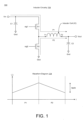
- Figure 1 illustrates a schematic diagram of inductor circuitry in accordance with various implementations described herein.
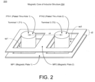
- Figure 2 illustrates a diagram of a magnetic core of an inductor structure in accordance with various implementations described herein.
- Figure 3 illustrates a diagram of a substrate with embedded magnetic core of an inductor structure in accordance with various implementations described herein.
- Figures 4A-4B illustrate diagrams of a substrate with embedded magnetic core of an inductor structure in accordance with implementations described herein.
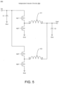
- Figure 5 illustrates a diagram of independent inductor circuitry in accordance with implementations described herein.
- Figure 6 illustrates a diagram of coupled inductor circuitry in accordance with implementations described herein.
- Figure 7 illustrates a diagram of a magnetic core of an inductor structure in accordance with various implementations described herein.
- Figure 8 illustrates a diagram of a substrate with embedded magnetic core of an inductor structure in accordance with various implementations described herein.
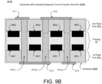
- Figures 9A-9B illustrate diagrams of a substrate with embedded magnetic core of an inductor structure in accordance with implementations described herein.
- Figure 10 illustrates a diagram of inductor circuitry with embedded capacitor in accordance with various implementations described herein.
- Figure 11 illustrates a diagram of a substrate with embedded inductor structure and capacitor in accordance with various implementations described herein.
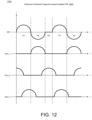
- Figure 12 illustrates a diagram of resonant switched capacitor based isolated integrated voltage regulator in accordance with implementations described herein.
DETAILED DESCRIPTION
-
Various implementations described herein are directed to embedded inductor schemes and techniques for various circuit related applications in physical designs. Also, in some implementations, various embedded inductor schemes and techniques described herein provide for novel package substrate cores with embedded inductors for integrated voltage regulators (IVRs). Objectives of the embedded inductor structures described herein may be used to improve the energy density of IVRs (integrated voltage regulators, such as, e.g., voltage regulator inside the package/die). Also, objectives of the embedded inductor structures described herein may provide a larger Q-factor for inductors to improve power conversion efficiency in various circuit based applications. In addition, objectives of the embedded inductor structures described herein may also improve manufacturability with the same/larger inductance values. Further, objectives of the embedded inductor structures described herein may reduce space usage of IVRs, including, e.g., reducing area used by inductor structures, which may reduce system integration difficulty and may increase power density.
-
Various implementations of embedded inductor schemes and techniques for circuit based applications will now be described herein in Figures 1-12.
-
Figure 1 illustrates a diagram 100 of inductor circuitry 104 in accordance with various implementations described herein.
-
In some implementations, the inductor circuitry 104 may provide for fabricating embedded inductor related circuitry with various integrated circuit (IC) components that are arranged and/or coupled together as an assemblage or some combination of parts that provide for physical circuit designs and structures. In some instances, a method of designing, providing and fabricating the inductor circuitry 104 as an integrated device may involve use of various circuit components and/or related structures described herein so as to implement various embedded inductor techniques associated therewith. Also, the inductor circuitry 104 may be integrated with various circuitry and/or related components on a single chip, and the inductor circuitry 104 may be implemented in some embedded devices for various automotive, mobile, computer, server and/or Internet-of-Things (IoT) based applications, including remote sensor nodes.
-
As shown in Figure 1, the inductor circuitry 104 may have an inductor structure with an inductor coil (IC) disposed between multiple terminals (T1, T2). The inductor circuitry 104 may have multiple switches (S1, S2) coupled in series between input voltage node (Vin) and ground (Vss or Gnd). Also, the inductor circuitry 104 may include an input capacitor (C1) coupled between input voltage supply (Vin) and ground (Vss or Gnd), and the inductor circuitry 104 may include an output capacitor (C2) coupled between an output voltage node (Vout) and ground (Vss or Gnd). The switches (S1, S2) may include a first switch (S1) coupled between the input voltage node (Vin) and a first terminal (T1) of the inductor coil (IC), and the switches (S1, S2) may include a second switch (S2) coupled between the first terminal (T1) of the inductor coil (IC) and ground (Vss or Gnd). The first terminal (T1) of the inductor coil (IC) may be coupled to a node disposed between the switches (S1, S2). Also, a second terminal (T2) of the inductor coil (IC) may be coupled to the output voltage node (Vout). The first transistor (S1) may be activated by a first activation signal (sig1) coupled to a gate thereof, and the second transistor (S2) may be activated by a second activation signal (sig2) coupled to a gate thereof. In various instances, the switches (S1, S2) may be implemented with various devices, such as, e.g., n-type transistors, p-type transistors, or some combination thereof.
-
In addition, Figure 1 shows a waveform diagram 124 that depicts the expected waveforms P1 and P2 corresponding to the inductor circuitry 104, wherein the waveform P1 provides an increasing current rise of a ripple signal passing through the inductor circuitry 104, and wherein the waveform P2 provides a decreasing current fall of the ripple signal passing through the inductor circuitry 104. The ripple signal may refer to current (i_L) through the inductor circuitry 104 per unit time (t). The inductance value of inductor coil (IC) corresponding to the inductor circuitry 104 may be large enough to keep the output current ripple small so as to have a small output ripple voltage. For instance, in some scenarios, the input voltage may be approximately 1V to 2.5V, and the inductor circuitry 104 may provide the output voltage at approximately 0.4 V to 1.2V. However, various other values, behaviors and characteristics may be achieved with different inputoutput voltages.
-
Figure 2 illustrates a diagram 200 of a magnetic core of an inductor structure 204 in accordance with various implementations described herein.
-
In some implementations, the inductor structure 204 may provide for fabricating embedded inductor related circuitry with various integrated circuit (IC) components that are arranged and/or coupled together as an assemblage or some combination of parts so as to provide for physical circuit designs and structures. In some instances, a method of designing, providing and fabricating the inductor structure 204 as an integrated device may involve use of various circuit components and/or related structures described herein so as to implement various embedded inductor techniques associated therewith. Also, the inductor structure 204 may be integrated with various circuitry and/or various related components on a single chip, and also, the inductor structure 204 may be implemented in some embedded devices for various automotive, mobile, computer, server and/or loT based applications, including remote sensor nodes.
-
As shown in Figure 2, the inductor structure 204 may include magnetic plates (MP1, MP2) embedded within a substrate (e.g., shown in Figure 3) having a first magnetic flux, and also, the inductor structure 204 may include one or more conductive cylinders or one or more plated thru-holes (PTH1, PTH2) that may be configured to provide an electric path that passes through the magnetic plates (MP1, MP2). In various instances, the magnetic plates (MP1, MP2) may be configured to enable a second magnetic flux within the magnetic plates (MP1, MP2) such that the second magnetic flux is greater than the first magnetic flux corresponding to the substrate. Thus, the one or more conductive cylinders (PTH1, PTH2) may refer to one or more plated thru-holes that pass through the magnetic plates (MP1, MP2) of the inductor structure 204.
-
In some instances, the PTH (plated-thru-hole) refers to a type of structure that provides interconnection between two layers, such as, e.g., two metal layers, including two copper layers, on top and bottom of a dielectric layer. Also, in some instances, the structure may be formed by drilling a hole first and then plating the hole with a conductive material, such as, e.g., a metal, including copper. Also, in some other instances, a PTH (plated-thru-hole) or via may refer to a hole that is created within a substrate that connects one or more layers. For instance, after a hole is created by mechanical drilling, chemical etching, laser ablation or any other similar mechanism, the hole is then filled or lined with an electrically and/or thermally conductive material through any combination of plating, deposition, liquid filling, plugging or other via filling mechanism.
-
In some implementations, the one or more conductive cylinders (PTH1, PTH2) may have a first conductive cylinder comprising a first plated thru-hole (PTH1) that passes through a first opening or first aperture (op1) formed in each of the magnetic plates (MP1, MP2) of inductor structure 204. The one or more conductive cylinders (PTH1, PTH2) may have a second conductive cylinder comprising a second plated thru-hole (PTH2) that passes through a second opening or second aperture (op2) formed in each of magnetic plates (MP1, MP2) of inductor structure 204. The first plated thru-hole (PTH1) may refer to a node that corresponds to the first terminal (T1) of the inductor coil (IC) as shown in Figure 1, and the second plated thru-hole (PTH2) may refer to a node that corresponds to the second terminal (T2) of the inductor coil (IC) as shown in Figure 1.
-
In some implementations, the magnetic plates (MP1, MP2) may include a first magnetic plate (MP1) and a second magnetic plate (MP2) that may be formed of various magnetic materials, such as, e.g., ferrite with ur = 1000, having various thicknesses, such as, e.g., 10um. Also, the plated thru-holes (PTH1, PTH2) may be displaced horizontally at a first distance (d1), such as, e.g., of approximately 500um, and further, the magnetic plates (MP1, MP2) may be displaced vertically at a second distance (d2), such as, e.g., of approximately 400um. In various other instances, the second distance (d2) may include any range of values between approximately 50um and 1.2mm, including, e.g., any value of approximately 50um, 100um, 200, 800um, 1mm and/or 1.2mm.
-
Figure 3 illustrates a diagram 300 of a substrate 308 with embedded magnetic core 318 of inductor structure 304 in accordance with various implementations described herein. Figure 3 has similar corresponding features to that shown in Figure 2.
-
In some implementations, the inductor structure 304 may provide for fabricating embedded inductor related circuitry with various integrated circuit (IC) components that are arranged and/or coupled together as an assemblage or some combination of parts so as to provide for physical circuit designs and structures. In some instances, a method of designing, providing and fabricating the inductor structure 304 as an integrated device may involve use of various circuit components and/or related structures described herein so as to implement various embedded inductor techniques associated therewith. Also, the inductor structure 304 may be integrated with various circuitry and/or various related components on a single chip, and also, the inductor structure 304 may be implemented in some embedded devices for various automotive, mobile, computer, server and/or loT based applications, including remote sensor nodes.
-
As shown in Figure 3, the substrate 308 may include multiple layers, including, e.g., a first substrate layer SL1, a second substrate layer SL2, and a third substrate layer SL3, that are integrated together to form the substrate 308. In some implementations, the embedded magnetic core 318 may be formed within the second substrate layer SL2, and also, the first substrate layer SL1 and the third substrate layer SL3 may include conductive lines (CL) and conductive bumps (CB) that are used to electrically couple the IVR die 324 to the CPU die 328. Also, the IVR die 324 refers to an integrated voltage regulator (IVR), and the CPU die 328 refers to a central processing unit (CPU). In some instances, so as to implement the inductor together with the IVR, one approach is to place the IVR beside the CPU core so they share a common heat sink to avoid thermal issues.
-
In various implementations, the multiple layers (e.g., SL1, SL2, SL3) may refer to any number of layers and/or any combination of layers. Also, in reference to Figure 3, each layer (e.g., SL1, SL2, SL3) may refer to a group of layers or layer group having one or more layers within each layer group, such as, e.g., the first substrate layer (SL1) may refer to a first substrate layer group, and so on, wherein each substrate layer (e.g., SL2, SL3) may refer to a substrate layer group. Also, in some instances, a coreless substrate may be used so that there may not be a clear visible delineation of the substrate groups, wherein the magnetic layers may be inserted in an internal pair of layers.
-
In various implementations, as described herein, the inductor structure 304 may include the magnetic plates (MP1, MP2) embedded within the substrate 308 having a first magnetic flux, and also, the inductor structure 304 may include one or more conductive cylinders or plated thru-holes (PTH1, PTH2) that are configured to provide an electric path that passes through magnetic plates (MP1, MP2). Also, as described herein, the magnetic plates (MP1, MP2) enable a second magnetic flux within the magnetic plates (MP1, MP2) such that the second magnetic flux is greater than the first magnetic flux.
-
In some implementations, the conductive cylinders or plated thru-holes (PTH1, PTH2) include a first plated thru-hole (PTH1) and a second plated thru-hole (PTH2), and conductive lines (CL1, CL2, CL3) may be used to electrically couple the IVR die 324 to the CPU die 328. For instance, the conductive lines (CL1, CL2, CL3) may include a first conductive line (CL1) electrically coupled to a first end of the first plated thru-hole (PTH1), a second conductive line (CL2) electrically coupled to a first end of the second plated thru-hole (PTH2), and a third conductive line (CL3) electrically coupled to second ends of the first plated thru-hole (PTH1) and the second plated thru-hole (PTH2). The third conductive line (CL3) electrically couples the first plated thru-hole (PTH1) to the second plated thru-hole (PTH2) so as to provide the electric path through the inductor structure 318 between the first conductive line (CL1) to the second conductive line (CL2).
-
In various implementations, the substrate 308 may have a prepreg layer (SL2) and multiple rigid cores (SL1, SL3) such that the prepreg layer (SL2) is disposed between the multiple rigid cores (SL1, SL3). Also, as shown, the magnetic plates (MP1, MP2) may be embedded within the prepreg layer (SL2), and also, the conductive cylinders or plated thru-holes (PTH1, PTH2) may pass through the multiple rigid cores (SL1, SL3) and the prepreg layer (SL2) of the substrate 308. As shown and described in Figure 4A, the first and third substrate layers (SL1, SL3) may be rigid core layers, and the second substrate layer (SL2) may be a prepreg layer. In other instances, as shown in Figure 4B, the first and third substrate layers (SL1, SL3) may be prepreg layers, and the second substrate layer (SL2) may be a rigid core layer.
-
In some implementations, the magnetic plates (MP1, MP2) are embedded into the substrate core (e.g., prepreg layer) by using a rigid core material (e.g., BT, ABF, Epoxy, etc.) that provides stiffness to support the substrate and the dielectric material (or prepreg material), which is flexible (e.g., Polyimide, Polyamide resin). Since the dielectric material or prepreg material is more flexible than the rigid core material, then the magnetic plates (MP1, MP2) may be pushed into the substrate after processing. In some instances, the magnetic plates (MP1, MP2) may be used to increase permeability so that a magnetic field inside the material is much stronger, and as such, the magnetic plates (MP1, MP2) may provide an area having a much-strengthened magnetic field flux or density. Also, the prepreg layers and rigid core layers may include any type of dielectric material, including, in some instances, dielectric core layers may be implemented as prepreg layers.
-
Figures 4A-4B illustrate diagrams of a substrate with embedded magnetic core of an inductor structure in accordance with various implementations described herein. In particular, Figure 4A shows a diagram 404A of a substrate 408A with embedded magnetic core of an inductor structure 404A, and Figure 4B shows a diagram 404B of the substrate 408B with embedded magnetic core of an inductor structure 404B.
-
In some implementations, as shown in Figure 4A, the substrate 408A may have multiple layers, including, e.g., first rigid core layer (RC1), prepreg layer (PP), and second rigid core layer (RC2), wherein the prepreg layer (PP) is disposed between the rigid core layers (RC1, RC2). Also, as shown in the cross-sectional view of indictor structure 404A, the magnetic core may include magnetic plates (MP1, MP2) with magnetic segments (MS1, MS2) formed in the prepreg layer (PP).
-
In some implementations, the conductive cylinders or plated thru-holes (PTH1, PTH2) include the first plated thru-hole (PTH1) and the second plated thru-hole (PTH2), and conductive lines (CL1, CL2, CL3) may be used to electrically couple the plated thru-holes (PTH1, PTH2) together so as to form an electric path therethrough. For instance, the conductive lines (CL1, CL2, CL3) may include first conductive line (CL1) electrically coupled to the first end of first plated thru-hole (PTH1), the second conductive line (CL2) electrically coupled to the first end of the second plated thru-hole (PTH2), and the third conductive line (CL3) electrically coupled to second ends of first plated thru-hole (PTH1) and the second plated thru-hole (PTH2). Also, as shown in Figure 4A, the third conductive line (CL3) electrically couples the first plated thru-hole (PTH1) to the second plated thru-hole (PTH2) so as to provide the electric path through the inductor structure 404A between the first conductive line (CL1) to the second conductive line (CL2).
-
Therefore, in some implementations, as shown in Figure 4A, the substrate 408A has a prepreg layer (PP) and multiple rigid cores (RC1, RC2) such that the prepreg layer (PP) is disposed between the multiple rigid cores (RC1, RC2). Also, the magnetic plates (MP1, MP2) with magnetic segments (MS1, MS2) are embedded within the prepreg layer (PP), and the one or more conductive cylinders (PTH1, PTH2) pass through the multiple rigid cores (RC1, RC2) and the prepreg layer (PP) of the substrate 408A.
-
In some implementations, as shown in Figure 4B, the substrate 408B may have multiple layers, including, e.g., first prepreg (pre-impregnated) layer (PP1), rigid core layer (RC), and second prepreg layer (PP2), wherein the rigid core layer (RC) is disposed between the prepreg layers (PP1, PP2). Also, as shown in cross-sectional view of indictor structure 404B, the magnetic core may include magnetic plates (MP1, MP2) with magnetic segments (MS1, MS2) formed in the prepreg layers (PP1, PP2).
-
In some implementations, the conductive cylinders or plated thru-holes (PTH1, PTH2) include the first plated thru-hole (PTH1) and the second plated thru-hole (PTH2), and conductive lines (CL1, CL2, CL3) may be used to electrically couple the plated thru-holes (PTH1, PTH2) together so as to form an electric path therethrough. For instance, the conductive lines (CL1, CL2, CL3) may include first conductive line (CL1) electrically coupled to the first end of first plated thru-hole (PTH1), the second conductive line (CL2) electrically coupled to the first end of the second plated thru-hole (PTH2), and the third conductive line (CL3) electrically coupled to second ends of first plated thru-hole (PTH1) and the second plated thru-hole (PTH2). Also, as shown in Figure 4B, the third conductive line (CL3) electrically couples the first plated thru-hole (PTH1) to the second plated thru-hole (PTH2) so as to provide the electric path through the inductor structure 404B between the first conductive line (CL1) to the second conductive line (CL2).
-
Therefore, in some implementations, as shown in Figure 4B, the substrate 408B has a rigid core (RC) and multiple prepreg cores (PP1, PP2) such that the rigid core (RC) is disposed between the multiple prepreg layers(PP1, PP2). Also, the magnetic plates (MP1, MP2) with magnetic segments (MS1, MS2) are embedded within the multiple prepreg layers (PP1, PP2), and the one or more conductive cylinders (PTH1, PTH2) pass through prepreg layers (PP1, PP2) and rigid core (RC) of substrate 408B.
-
Also, in various implementations, in reference to Figures 4A-4B, the multiple substrate layers (e.g., RC1/PP/RC2 and PP1/RC/PP2) may refer to any number of layers and/or any combination of layers. Also, each layer (e.g., RC1/PP/RC2 and PP1/RC/PP2) may refer to a group of layers or layer group having one or more layers within each layer group, such as, e.g., each PP layer may refer to a PP layer group, and so on, wherein each substrate layer (e.g., RC1/PP/RC2 and PP1/PP/PP2) may refer to a substrate layer group. Also, in some instances, a coreless substrate may be used so that there may not be a clear visible delineation of the substrate groups, wherein the magnetic layers may be inserted in an internal pair of dielectric layers, in some applications.
-
Figure 5 illustrates a schematic diagram 500 of independent inductor circuitry 504 in accordance with various implementations described herein.
-
In some implementations, the inductor circuitry 504 may provide for fabricating embedded inductor related circuitry with various integrated circuit (IC) components that are arranged and/or coupled together as an assemblage or some combination of parts that provide for physical circuit designs and structures. In some instances, a method of designing, providing and fabricating the inductor circuitry 504 as an integrated device may involve use of various circuit components and/or related structures described herein so as to implement various embedded inductor techniques associated therewith. Also, the inductor circuitry 504 may be integrated with various circuitry and/or related components on a single chip, and the inductor circuitry 504 may be implemented in some embedded devices for various automotive, mobile, computer, server and/or Internet-of-Things (IoT) based applications, including remote sensor nodes.
-
As shown in Figure 5, the inductor circuitry 504 may have an inductor structure with independent inductor coils (IC1, IC2), including, e.g., first inductor coil (IC1) disposed between terminals (T1, T2) and second inductor coil (IC2) disposed between terminals (T3, T4). The inductor circuitry 504 may include multiple sets of switches (S1/S2 and S3/S4) separately coupled in series between the input voltage node (Vin) and ground (Vss or Gnd). In some instances, the inductor circuitry 504 may have the input capacitor (C1) coupled between the input voltage supply (Vin) and ground (Vss or Gnd), and also, the inductor circuitry 504 may have the output capacitor (C2) coupled between the output voltage node (Vout) and ground (Vss or Gnd).
-
Also, the switches (S1, S2) may have the first switch (S1) coupled between the input voltage node (Vin) and the first terminal (T1) of the first inductor coil (IC1), and also, the switches (S1, S2) may have the second switch (S2) coupled between the first terminal (T1) of the first inductor coil (IC1) and ground (Vss or Gnd). The first terminal (T1) of first inductor coil (IC1) may be coupled to a node disposed between the switches (S1, S2). The second terminal (T2) of first inductor coil (IC1) may be coupled to the output voltage node (Vout). The first transistor (S1) may be activated by the first activation signal (sig1) coupled to a gate thereof, and the second transistor (S2) may be activated by the second activation signal (sig2) coupled to a gate thereof. In various instances, the switches (S1, S2) may be implemented with various devices, such as, e.g., n-type transistors, p-type transistors, or some combination thereof.
-
Also, the switches (S3, S4) may have a third switch (S3) coupled between the input voltage node (Vin) and a third terminal (T3) of the second inductor coil (IC2), and the switches (S3, S4) may have a fourth switch (S4) coupled between the third terminal (T3) of the second inductor coil (IC2) and ground (Vss or Gnd). The third terminal (T3) of second inductor coil (IC2) may be coupled to a node disposed between switches (S3, S4). Also, a fourth terminal (T4) of second inductor coil (IC2) may be coupled to the output voltage node (Vout). In some instances, a third transistor (S3) may be activated by a third activation signal (sig3) coupled to a gate thereof, and a fourth transistor (S4) may be activated by a fourth activation signal (sig4) coupled to a gate thereof. In various instances, the switches (S3, S4) may be implemented with various devices, such as, e.g., n-type transistors, p-type transistors, or some combination thereof.
-
Thus, in various implementations, the independent inductor circuitry 504 may include a plurality of inductor structures (IC1, IC2) embedded within a substrate, and also, the inductor structures (IC1, IC2) may have a first inductor structure (IC1) that provides a first magnetic flux with first magnetic plates embedded within the substrate, and also, the inductor structures (IC1, IC2) may have a second inductor structure (IC2) that provides a second magnetic flux with second magnetic plates embedded within the substrate. Also, the first inductor structure (IC1) may provide a first electric path with first plated thru-holes (PTH) that pass through the first magnetic plates, and also, wherein the second inductor structure (IC2) may provide a second electric path with second plated thru-holes (PTH) that pass through the second magnetic plates. Further description related to the inductor structures (IC1, IC2), the plated thru-holes (PTH), and magnetic plates (MP) are provided herein in greater detail with reference to Figure 7.
-
In various implementations, in reference to combination of Figures 5 and 7, the first inductor structure (IC1) is separate and distinct from second inductor structure (IC2), and as described herein, the substrate has a first magnetic flux. Also, the first magnetic plates (MP1) enable a second magnetic flux within first magnetic plates (MP1) such that the second magnetic flux'is greater than the first magnetic flux, and the second magnetic plates (MP2) enable a third magnetic flux within the second magnetic plates such that the third magnetic flux is greater than the first magnetic flux.
-
As described in reference to Figure 4A, the substrate may have a prepreg (PP) disposed between multiple rigid cores (RC1, RC2), and the first magnetic plates (MP1) and the second magnetic plates (MP2) may be embedded within the prepreg (PP) of the substrate. Also, the first plated thru-holes (PTH1) and the second plated thru-holes (PTH2) pass through the multiple rigid cores (RC1, RC2) and prepreg (PP) of the substrate.
-
As described in reference to Figure 4B, the substrate may include a rigid core (RC) disposed between multiple prepreg layers (PP1, PP2), and the first magnetic plates (MP1) and the second magnetic plates (MP2) may be embedded within the multiple prepreg layers (PP1, PP2) of the substrate. Also, the first plated thru-holes (PTH1) and the second plated thru-holes (PTH2) pass through the multiple prepreg layers (PP1, PP2) and the rigid core (RC) of the substrate.
-
Figure 6 illustrates a schematic diagram 500 of coupled inductor circuitry 604 in accordance with various implementations described herein.
-
In some implementations, the inductor circuitry 604 may provide for fabricating embedded inductor related circuitry with various integrated circuit (IC) components that are arranged and/or coupled together as an assemblage or some combination of parts that provide for physical circuit designs and structures. In some instances, a method of designing, providing and fabricating the inductor circuitry 604 as an integrated device may involve use of various circuit components and/or related structures described herein so as to implement various embedded inductor techniques associated therewith. Also, the inductor circuitry 604 may be integrated with various circuitry and/or related components on a single chip, and the inductor circuitry 604 may be implemented in some embedded devices for various automotive, mobile, computer, server and/or Internet-of-Things (IoT) based applications, including remote sensor nodes.
-
As shown in Figure 6, the inductor circuitry 604 may have an inductor structure with coupled inductor coils (IC1, IC2), including, e.g., the first inductor coil (IC1) disposed between terminals (T1, T2) and the second inductor coil (IC2) disposed between terminals (T3, T4). Also, the inductor circuitry 604 may include the multiple sets of switches (S1/S2 and S3/S4) separately coupled in series between the input voltage node (Vin) and ground (Vss or Gnd). Also, in various implementations, the inductor circuitry 604 may include the input capacitor (C1) coupled between input voltage supply (Vin) and ground (Vss or Gnd), and also, the inductor circuitry 604 may have the output capacitor (C2) coupled between the output voltage node (Vout) and ground (Vss or Gnd).
-
Also, the switches (S1, S2) may have the first switch (S1) coupled between the input voltage node (Vin) and the first terminal (T1) of the first inductor coil (lC1), and also, the switches (S1, S2) may have the second switch (S2) coupled between the first terminal (T1) of the first inductor coil (IC1) and ground (Vss or Gnd). The first terminal (T1) of first inductor coil (IC1) may be coupled to a node disposed between the switches (S1, S2). The second terminal (T2) of first inductor coil (IC1) may be coupled to the output voltage node (Vout). The first transistor (S1) may be activated by the first activation signal (sig1) coupled to the gate thereof, and the second transistor (S2) may be activated by second activation signal (sig2) coupled to the gate thereof. In some instances, the switches (S1, S2) may be implemented with various devices, such as, e.g., n-type transistors, p-type transistors, or some combination thereof.
-
Also, the switches (S3, S4) may have the third switch (S3) coupled between the input voltage node (Vin) and the third terminal (T3) of the second inductor coil (IC2), and the switches (S3, S4) may have the fourth switch (S4) coupled between the third terminal (T3) of the second inductor coil (IC2) and ground (Vss or Gnd). The third terminal (T3) of second inductor coil (IC2) may be coupled to a node disposed between switches (S3, S4). The fourth terminal (T4) of the second inductor coil (IC2) may be coupled to the output voltage node (Vout). The third transistor (S3) may be activated by the third activation signal (sig3) coupled to the gate thereof, and the fourth transistor (S4) may be activated by the fourth activation signal (sig4) coupled to the gate thereof. Also, in various instances, the switches (S3, S4) may be implemented with various devices, such as, e.g., n-type transistors, p-type transistors, or some combination thereof.
-
Thus, in various implementations, the coupled inductor circuitry 604 may have a plurality of inductor structures (IC1, IC2) embedded within a substrate, and the inductor structures (IC1, IC2) may have a first inductor structure (IC1) that provides a first magnetic flux with first magnetic plates embedded within the substrate, and the inductor structures (IC1, IC2) may have a second inductor structure (IC2) that provides a second magnetic flux with second magnetic plates embedded within the substrate. The first inductor structure (IC1) and the second inductor structure (IC2) are electrically coupled together so as to provide parallel electric paths through the first and second magnetic plates. Further description related to inductor structures (IC1, IC2), plated thru-holes (PTH), and magnetic plates (MP) are provided herein in greater detail with reference to Figure 7.
-
In various implementations, in reference to combination of Figures 6 and 7, the first inductor structure (IC1) may provide a first electric path with first plated thru-holes (PTH1) that pass through the first magnetic plates (MP1), and also, the second inductor structure (IC2) may provide a second electric path with second plated thru-holes (PTH2) that pass through second magnetic plates (MP2). Also, the first inductor structure (IC1) may have a separate structure that is coupled together with the second inductor structure (IC2). In some instances, as shown in Figure 4A, the substrate may have a prepreg layer (PP) disposed between multiple rigid cores (RC1, RC2), and the first magnetic plates (MP1) and the second magnetic plates (MP2) may be embedded within the prepreg layer (PP) of the substrate. As shown in Figure 4B, the substrate may include a rigid core (RC) disposed between multiple prepreg layers (PP1, PP2), and also, the first magnetic plates (MP1) and the second magnetic plates (MP2) may be embedded within the multiple prepreg layers (PP1, PP2) of the substrate.
-
Figure 7 illustrates a diagram 700 of a magnetic core of an inductor structure 704 in accordance with various implementations described herein.
-
In some implementations, the inductor structure 704 may provide for fabricating embedded inductor related circuitry with various integrated circuit (IC) components that are arranged and/or coupled together as an assemblage or some combination of parts so as to provide for physical circuit designs and structures. In some instances, a method of designing, providing and fabricating the inductor structure 704 as an integrated device may involve use of various circuit components and/or related structures described herein so as to implement various embedded inductor techniques associated therewith. Also, the inductor structure 704 may be integrated with various circuitry and/or various related components on a single chip, and also, the inductor structure 704 may be implemented in some embedded devices for various automotive, mobile, computer, server and/or loT based applications, including remote sensor nodes.
-
As shown in Figure 7, the inductor structure 704 may include magnetic plates (MP1, MP2) embedded within a substrate (e.g., shown in Figure 3) having a first magnetic flux, and also, the inductor structure 704 may include conductive cylinders or plated thru-holes (PTH1, PTH2, PTH3, PTH4) that may be configured to provide one or more electric paths that pass through the magnetic plates (MP1, MP2). Also, in various instances, the magnetic plates (MP1, MP2) may be configured to enable a second magnetic flux within the magnetic plates (MP1, MP2) such that the second magnetic flux is greater than the first magnetic flux corresponding to the substrate. Thus, the conductive cylinders (PTH1, PTH2, PTH3, PTH4) may refer to plated thru-holes (PTH) that pass through the magnetic plates (MP1, MP2) of the inductor structure 704.
-
In some implementations, the conductive cylinders (PTH1, PTH2, PTH3, PTH4) may have a first conductive cylinder comprising a first plated thru-hole (PTH1) that passes through the magnetic plates (MP1, MP2) of inductor structure 704. Also, the conductive cylinders (PTH1, PTH2, PTH3, PTH4) may have a second conductive cylinder comprising a second plated thru-hole (PTH2) that passes through the magnetic plates (MP1, MP2) of inductor structure 704. Also, the conductive cylinders (PTH1, PTH2, PTH3, PTH4) may have a third conductive cylinder comprising a third plated thru-hole (PTH3) that passes through the magnetic plates (MP1, MP2) of inductor structure 704. Also, the conductive cylinders (PTH1, PTH2, PTH3, PTH4) may have a fourth conductive cylinder comprising a fourth plated thru-hole (PTH4) that passes through the magnetic plates (MP1, MP2) of inductor structure 704.
-
In some implementations, the first plated thru-hole (PTH1) may refer to a node that corresponds to the first terminal (T1) of the first inductor coil (IC1) as shown in Figures 5-6, and the second plated thru-hole (PTH2) may refer to a node that corresponds to the second terminal (T2) of the first inductor coil (IC1) as shown in Figures 5-6. Also, in some instances, the third plated thru-hole (PTH3) may refer to a node that corresponds to the third terminal (T3) of the second inductor coil (IC2) as shown in Figures 5-6, and also, the fourth plated thru-hole (PTH4) may refer to a node that corresponds to the fourth terminal (T4) of the second inductor coil (IC2) as shown in Figures 5-6.
-
In some implementations, the inductor structures (IC1, IC2) may be configured to provide a multi-phase coupled inductor structure (e.g., as shown in Figure 6) with the first inductor structure (IC1) and the second inductor structure (IC2). Also, the first electric path (P0) may provide a first current direction for a first phase (e.g., direction of arrow for P0), and also, the second electric path (P1) may provide a second current direction for a second phase (e.g., direction of arrow for P1) that is opposite to the first current direction and the first phase.
-
Figure 8 illustrates a diagram 800 of a substrate 808 with embedded magnetic core 818 of inductor structure 804 in accordance with various implementations described herein. Figure 8 has similar corresponding features to that shown in Figure 3.
-
In some implementations, the inductor structure 804 may provide for fabricating embedded inductor related circuitry with various integrated circuit (IC) components that are arranged and/or coupled together as an assemblage or some combination of parts so as to provide for physical circuit designs and structures. In some instances, a method of designing, providing and fabricating the inductor structure 804 as an integrated device may involve use of various circuit components and/or related structures described herein so as to implement various embedded inductor techniques associated therewith. Also, the inductor structure 804 may be integrated with various circuitry and/or various related components on a single chip, and also, the inductor structure 804 may be implemented in some embedded devices for various automotive, mobile, computer, server and/or loT based applications, including remote sensor nodes.
-
As shown in Figure 8, the substrate 808 may include multiple layers, including, e.g., first substrate layer SL1, second substrate layer SL2, and third substrate layer SL3, that are integrated together to form substrate 808. In some implementations, embedded magnetic core 818 may be formed within the second substrate layer SL2, and also, the first substrate layer SL1 and the third substrate layer SL3 may have conductive lines (CL) and conductive bumps (CB) that are used to electrically couple IVR die 824 to CPU die 828. Also, the IVR die 824 refers to an integrated voltage regulator (IVR), and the CPU die 828 refers to a central processing unit (CPU).
-
In various implementations, as described herein, the inductor structure 804 may include the magnetic plates (MP1, MP2) embedded within the substrate 808 having a first magnetic flux, and also, the inductor structure 804 may include one or more conductive cylinders or plated thru-holes (PTH1) that is configured to provide an electric path that passes through magnetic plates (MP1, MP2). Thus, the one or more conductive cylinders may comprise a single plated thru-hole (PTH1) that passes through the magnetic plates (MP1, MP2) of the inductor structure 804. Also, as described herein, the magnetic plates (MP1, MP2) enable a second magnetic flux within the magnetic plates (MP1, MP2) such that the second magnetic flux is greater than the first magnetic flux.
-
In various implementations, the conductive cylinder or plated thru-hole (PTH1) may only include the first plated thru-hole (PTH1), and conductive lines (CL1, CL2, CL3) may be used to electrically couple the IVR die 824 that is mounted to the first substrate layer (SL1) to the CPU die 828 that is mounted to the third substrate layer (SL3). For instance, conductive lines (CL1, CL2, CL3) may have a first conductive line (CL1) electrically coupled to a first end of the first plated thru-hole (PTH1), a second conductive line (CL2) electrically coupled to a second end of the first plated thru-hole (PTH1). As such, in some instances, the first and second conductive lines (CL1, CL2) electrically couple the IVR die 824 to the CPU die 828 by way of the first plated thru-hole (PTH1) so as to thereby provide the electric path through the inductor structure 818 between the first conductive line (CL1) and the second conductive line (CL2).
-
In various implementations, the substrate 808 may have a prepreg layer (SL2) and multiple rigid cores (SL1, SL3) such that the prepreg layer (SL2) is disposed between the multiple rigid cores (SL1, SL3). Also, as shown, the magnetic plates (MP1, MP2) may be embedded within the prepreg layer (SL2), and also, the conductive cylinder or plated thru-hole (PTH1) may pass through the multiple rigid cores (SL1, SL3) and the prepreg layer (SL2) of the substrate 808. As shown and described in Figure 4A, the first and third substrate layers (SL1, SL3) may be rigid core layers, and the second substrate layer (SL2) may be a prepreg layer. In other instances, as shown in Figure 4B, the first and third substrate layers (SL1, SL3) may be prepreg layers, and the second substrate layer (SL2) may be a rigid core layer.
-
Figures 9A-9B illustrate diagrams of a substrate with embedded magnetic core of an inductor structure in accordance with various implementations described herein. In particular, Figure 9A shows a diagram 900A of a substrate 908A with embedded magnetic core of an inductor structure 904A, and Figure 9B shows a diagram 900B of a substrate 908B with embedded magnetic core of an inductor structure 904B. Figures 9A-9B have similar corresponding features to that shown in Figures 4A-4B.
-
In some implementations, as shown in Figure 9A, the substrate 908A may have multiple layers, including, e.g., first rigid core layer (RC1), prepreg layer (PP), and second rigid core layer (RC2), wherein the prepreg layer (PP) is disposed between the rigid core layers (RC1, RC2). Also, as shown in the cross-sectional view of indictor structure 904A, the magnetic core may include magnetic plates (MP1, MP2) with magnetic segments (MS1, MS2) formed in the prepreg layer (PP).
-
In some implementations, the conductive cylinder or plated thru-hole (PTH1) include only the first plated thru-hole (PTH1), and the conductive lines (CL1, CL3) may be used to electrically couple the plated thru-hole (PTH1) to the conductive lines (CL1, CL3) so as to form an electric path therethrough. Thus, the conductive cylinder may comprise only a single plated thru-hole (PTH1) that passes through the magnetic plates (MP1, MP2) having the magnetic segments (MS1, MS2) of the inductor structure 904A.
-
In some implementations, as shown in Figure 9B, the substrate 908B may have multiple layers, including, e.g., first rigid core layer (RC1), prepreg layer (PP), and second rigid core layer (RC2), wherein the prepreg layer (PP) is disposed between the rigid core layers (RC1, RC2). Also, as shown in the cross-sectional view of indictor structure 904B, the magnetic core may include magnetic plates (MP1, MP2) with magnetic segments (MS1, MS2) formed in the prepreg layer (PP).
-
In some implementations, the conductive cylinders or plated thru-holes (PTH1, PTH2, PTH3) may include first plated thru-hole (PTH1), second plated thru-hole (PTH2), and third plated thru-hole (PTH3) along with conductive lines (CL1, CL2, CL3, CL4) may be used to electrically couple the plated thru-holes (PTH1, PTH2, PTH3) to the conductive lines (CL1, CL2, CL3, CL4) so as to form an electric path therethrough. As such, in some instances, the multiple conductive cylinders may comprise at least three plated thru-holes (PTH1, PTH2, PTH3) that pass through the magnetic plates (MP1, MP2) with magnetic segments (MS1, MS2) of the inductor structure 904B.
-
Figure 10 illustrates a diagram 1000 of inductor circuitry 1004 with embedded capacitor (EC) in accordance with various implementations described herein.
-
In some implementations, the inductor circuitry 1004 may provide for fabricating embedded inductor related circuitry with various integrated circuit (IC) components that are arranged and/or coupled together as an assemblage or some combination of parts that provide for physical circuit designs and structures. In some instances, a method of designing, providing and fabricating the inductor circuitry 1004 as an integrated device may involve use of various circuit components and/or related structures described herein so as to implement various embedded inductor techniques associated therewith. Also, the inductor circuitry 1004 may be integrated with various circuitry and/or related components on a single chip, and the inductor circuitry 1004 may be implemented in some embedded devices for various automotive, mobile, computer, server and/or Internet-of-Things (IoT) based applications, including remote sensor nodes.
-
As shown in Figure 10, the inductor circuitry 1004 may include multiple inductor structures with coupled inductor coils (IC1/IC2 and IC3/IC4), including the first inductor coil (IC1) disposed between the terminals (T1, T2), the second inductor coil (IC2) disposed between the terminals (T3, T4), third inductor coil (IC3) disposed between terminals (T5, T6), and fourth inductor coil (IC4) disposed between terminals (T7, T8). Also, the inductor circuitry 1004 may include multiple sets of switches (S1/S2 and S3/S4) separately coupled in series with the coupled inductor coils (IC1/IC2 and IC3/IC4) between nodes (Vin/Vout) and ground (Vss or Gnd). Also, in some implementations, the inductor circuitry 1004 may include input capacitor (C1) coupled between input voltage supply (Vin) and ground (Vss or Gnd), and the inductor circuitry 1004 may have output capacitor (C2) coupled between the output voltage node (Vout) and ground (Vss or Gnd). Also, in some implementations, the inductor circuitry 1004 may include embedded capacitor (EC) coupled between input voltage supply (Vin or Vdd) and ground (Vss or Gnd).
-
Also, the switches (S1, S2) may have the first switch (S1) coupled between the input voltage node (Vin) and terminal (T1) of first inductor coil (IC1), and also, the switches (S1, S2) may have the second switch (S2) coupled between terminal (T4) of the second inductor coil (IC2) and the output voltage node (Vout). Also, terminal (T2) of first inductor coil (IC1) may be coupled to terminal (T3) of the second inductor coil (IC2). Also, the first switch (S1) may be activated by first activation signal (sig1), and the second switch (S2) may be activated by second activation signal (sig2). Also, in some instances, the switches (S1, S2) may be implemented with various devices, such as, e.g., n-type transistors, p-type transistors, or some combination thereof.
-
Also, the switches (S3, S4) may have the third switch (S3) coupled between the input ground node (Vss) and terminal (T5) of third inductor coil (IC3), and the switches (S3, S4) may have the fourth switch (S4) coupled between terminal (T8) of fourth inductor coil (IC4) and the output ground node (Vss). Also, terminal (T6) of third inductor coil (IC3) may be coupled to terminal (T7) of fourth inductor coil (IC4). Also, third switch (S3) may be activated by third activation signal (sig3), and the fourth switch (S4) may be activated by fourth activation signal (sig4). Also, in some instances, the switches (S3, S4) may be implemented with various devices, such as, e.g., n-type transistors, p-type transistors, or some combination thereof.
-
Thus, in various implementations, the coupled inductor circuitry 1004 may have a plurality of inductor structures (IC1, IC2, IC3, IC4) embedded within a substrate, and the inductor structures (IC1, IC2, IC3, IC4) may include the first inductor structure (IC1) that provides a first magnetic flux with first magnetic plates embedded within the substrate, and the inductor structures (IC1, IC2, IC3, IC4) may include the second inductor structure (IC2) that provides a second magnetic flux with second magnetic plates embedded within the substrate. Also, the first inductor structure (IC1) and the second inductor structure (IC2) are electrically coupled together so as to provide a first combined electric path (lout) by way of Vin and Vout through the first and second magnetic plates.
-
Also, in various implementations, the coupled inductor circuitry 1004 may have a plurality of inductor structures (IC1, IC2, IC3, IC4) embedded within a substrate, and the inductor structures (IC1, IC2, IC3, IC4) may include the third inductor structure (IC3) that provides a third magnetic flux with third magnetic plates embedded within the substrate, and the inductor structures (IC1, IC2, IC3, IC4) may include the fourth inductor structure (IC4) that provides a fourth magnetic flux with fourth magnetic plates embedded within the substrate. Also, the third inductor structure (IC3) and fourth inductor structure (IC4) are electrically coupled together so as to provide another combined electric path by way of the ground line (Vss) through the third and fourth magnetic plates.
-
Also, in some implementations, the embedded capacitor (EC) may be disposed between a first set of inductor coils (IC1, IC3) and a second set of inductor coils (IC2, IC4) such that a current (IEC) may pass from node Vdd to node Vss through the embedded capacitor (EC). In reference to Figure 7, the embedded capacitor (EC) may be switched to assist with implementation of the embedded inductor structure so as to be extended to a two-phase coupled inductor. In this instance, current direction in the two pairs of PTHs are opposite to each other. Once there is a current change in one phase, there will be an induced current in the same direction of change in.the other phase. Therefore, the ripple current may be greatly reduced, and the total output di/dt may be improved.
-
Figure 11 illustrates a diagram 1100 of substrate 1108 with embedded inductor structure 1104 and embedded capacitor (EC) in accordance with various implementations described herein. Also, it should be appreciated that Figure 11 has similar corresponding features to that shown in Figure 9B.
-
In some implementations, as shown in Figure 11, the substrate 1108 may have multiple layers, including, e.g., first rigid core layer (RC1), prepreg layer (PP), and second rigid core layer (RC2), wherein the prepreg layer (PP) is disposed between the rigid core layers (RC1, RC2). Also, as shown in the cross-sectional view of indictor structure 1104, the magnetic core may include magnetic plates (MP1, MP2) with magnetic segments (MS1, MS2) formed in the prepreg layer (PP).
-
In some implementations, the conductive cylinders or plated thru-holes (PTH1, PTH2, PTH3) may include first plated thru-hole (PTH1), second plated thru-hole (PTH2), and third plated thru-hole (PTH3) along with conductive lines (CL1, CL2, CL3, CL4) may be used to electrically couple the plated thru-holes (PTH1, PTH2, PTH3) to the conductive lines (CL1, CL2, CL3, CL4) so as to form an electric path therethrough. As such, in some instances, the multiple conductive cylinders may comprise at least three plated thru-holes (PTH1, PTH2, PTH3) that pass through the magnetic plates (MP1, MP2) with magnetic segments (MS1, MS2) of the inductor structure 904B.
-
In various implementations, the inductor structure 1104 may have at least one embedded capacitor (EC) disposed between the magnetic plates (MP1, MP2), wherein the electric path passes through the embedded capacitor (EC) by way of at least one of the three plated thru-holes, such as, e.g., second plated thru-hole (PTH2). Also, in some instances, the first plated thru-hole (PTH1) passes through a first opening in each of the magnetic plates (MP1, MP2) of the inductor structure 1104, the second plated thru-hole (PTH2) passes through a second opening in each of the magnetic plates (MP1, MP2) of the inductor structure 1104, and the third plated thru-hole (PTH3) passes through a third opening in each of the magnetic plates (MP1, MP2) of the inductor structure 1104. Also, in some instances, as shown in Figure 11, the second conductive cylinder or the second plated thru-hole (PTH2) may comprise the embedded capacitor (EC).
-
Figure 12 illustrates a waveform diagram 1200 of a resonant switched capacitor based isolated integrated voltage regulator (IVR) in accordance with implementations described herein. Also, it should be appreciated that Figure 12 has similar corresponding features, behaviors and/or characteristics associated with Figures 10-11.
-
As shown in Figure 12, the waveform diagram 1200 refers to a graph of current (I) versus time (t) in multiple graphical representations of current (IEC) through embedded capacitor (EC) in Figures 10-11 when compared to various output currents (lout_1, lout_2, lout_3) from the inductor circuitry 1004 with the embedded capacitor (EC).
-
In various implementations, the switches (S1, S2, S3, S4) in Figure 10 may be controlled so that during P1, switches S1 and S3 are turned ON, so LC resonance occurs within the L (composed with PTH 2, CL2, and PTH3 and associated magnetics around) and EC. When the LC resonant current reaches back to zero, P2 starts, wherein S1 and S3 are turned OFF, and S2 and S4 are turned ON. The residual voltage in EC then forces the new LC loop to resonance within the L (composed with PTH1, CL3, and PTH2) and EC. During P2, IEC is negative, so lout is positive. There will be dead-time (DT in Figure 12) for another cycle (including P1 and P2) to start after. The DT is controlled so to have different conversion ratio or effective output current. It is desired to have >3 phases with 360/N (N is number of phases) degree apart from each other (whose current outputs are as shown in Figure 12), so to reduce output ripple voltage and increase efficiency. In this manner, an isolated LC resonance switched-cap converter may be realized.
-
It should be intended that the subject matter of the claims may not be limited to the implementations and illustrations provided herein, but include modified forms of those implementations including portions of implementations and combinations of elements of different implementations in accordance with the claims. It should be appreciated that in the development of any such implementation, as in any engineering or design project, numerous implementation-specific decisions should be made to achieve developers' specific goals, such as compliance with system-related and business related constraints, which may vary from one implementation to another. Moreover, it should be appreciated that such a development effort may be complex and time consuming, but would nevertheless be a routine undertaking of design, fabrication, and manufacture for those of ordinary skill having benefit of this disclosure.
-
Reference has been made in detail to various implementations, examples of which are illustrated in the accompanying drawings and figures. In the following detailed description, numerous specific details are set forth to provide a thorough understanding of the disclosure provided herein. However, the disclosure provided herein may be practiced without these specific details. In some other instances, well-known methods, procedures, components, circuits and networks have not been described in detail so as not to unnecessarily obscure details of the embodiments.
-
It should also be understood that, although the terms first, second, etc. may be used herein to describe various elements, these elements should not be limited by these terms. These terms are only used to distinguish one element from another. For example, a first element could be termed a second element, and, similarly, a second element could be termed a first element. The first element and the second element are both elements, respectively, but they are not to be considered the same element.
-
The terminology used in the description of the disclosure provided herein is for the purpose of describing particular implementations and is not intended to limit the disclosure provided herein. As used in the description of the disclosure provided herein and appended claims, the singular forms "a," "an," and "the" are intended to include the plural forms as well, unless the context clearly indicates otherwise. The term "and/or" as used herein refers to and encompasses any and all possible combinations of one or more of the associated listed items. The terms "includes," "including," "comprises," and/or "comprising," when used in this specification, specify a presence of stated features, integers, steps, operations, elements, and/or components, but do not preclude the presence or addition of one or more other features, integers, steps, operations, elements, components and/or groups thereof.
-
As used herein, the term "if" may be construed to mean "when" or "upon" or "in response to determining" or "in response to detecting," depending on the context. Similarly, the phrase "if it is determined" or "if [a stated condition or event] is detected" may be construed to mean "upon determining" or "in response to determining" or "upon detecting [the stated condition or event]" or "in response to detecting [the stated condition or event]," depending on the context. The terms "up" and "down"; "upper" and "lower"; "upwardly" and "downwardly"; "below" and "above"; and other similar terms indicating relative positions above or below a given point or element may be used in connection with some implementations of various technologies described herein.
-
While the foregoing is directed to implementations of various related techniques described herein, other and further implementations may be devised in accordance with the disclosure herein, which may be determined by the claims that follow.
-
Although the subject matter has been described herein in language specific to structural features and/or methodological acts, it should be understood that the subject matter defined in the appended claims is not necessarily limited to the specific features or acts described above. Rather, specific features and acts described above are disclosed as example forms of implementing the claims.
-
Implementations of the present disclosure may include:
- 1. An inductor structure comprising:
- magnetic plates embedded within a substrate having a first magnetic flux; and
- one or more conductive cylinders that provide an electric path that passes through the magnetic plates,
- wherein the magnetic plates enable a second magnetic flux within the magnetic plates such that the second magnetic flux is greater than the first magnetic flux.
- 2. The inductor structure of clause 1, wherein:
\ the one or more conductive cylinders comprise one or more plated thru-holes that pass through the magnetic plates of the inductor structure. - 3. The inductor structure of clause 2, wherein:
- the one or more conductive cylinders include a first conductive cylinder comprising a first plated thru-hole that passes through a first opening in each of the magnetic plates of the inductor structure, and
- the one or more conductive cylinders include a second conductive cylinder comprising a second plated thru-hole that passes through a second opening in each of the magnetic plates of the inductor structure.
- 4. The inductor structure of clause 3, further comprising:
- a first conductive line electrically coupled to a first end of the first plated thru-hole;
- a second conductive line electrically coupled to a first end of the second plated thru-hole; and
- a third conductive line electrically coupled to second ends of the first plated thru-hole and the second plated thru-hole,
- wherein the third conductive line electrically couples the first plated thru-hole to the second plated thru-hole so as to provide the electric path through the inductor structure between the first conductive line to the second conductive line.
- 5. The inductor structure of clause 1, wherein:
- the substrate has a dielectric core and multiple rigid cores such that the dielectric core is disposed between the multiple rigid cores,
- the magnetic plates are embedded within the dielectric core, and
- the one or more conductive cylinders pass through the multiple rigid cores and the dielectric core of the substrate.
- 6. The inductor structure of clause 1, wherein:
- the substrate has a rigid core and multiple dielectric cores such that the rigid core is disposed between the multiple dielectric cores,
- the magnetic plates are embedded within the multiple dielectric cores, and
- the one or more conductive cylinders pass through the multiple dielectric cores and the rigid core of the substrate.
- 7. The inductor structure of clause 1, wherein:
the one or more conductive cylinders comprise a single plated thru-hole that passes through the magnetic plates of the inductor structure. - 8. The inductor structure of clause 1, wherein:
the one or more conductive cylinders comprise three plated thru-holes that pass through the magnetic plates of the inductor structure. - 9. The inductor structure of clause 8, further comprising:
- an embedded capacitor disposed between the magnetic plates,
- wherein the electric path passes through the embedded capacitor by way of at least one of the three plated thru-holes.
- 10. The inductor structure of clause 8, wherein:
- the one or more conductive cylinders include a first conductive cylinder comprising a first plated thru-hole that passes through a first opening in each of the magnetic plates of the inductor structure,
- the one or more conductive cylinders include a second conductive cylinder comprising a second plated thru-hole that passes through a second opening in each of the magnetic plates of the inductor structure,
- the one or more conductive cylinders include a third conductive cylinder comprising a third plated thru-hole that passes through a third opening in each of the magnetic plates of the inductor structure, and
- the second conductive cylinder comprises an embedded capacitor.
- 11. A device comprising:
- a plurality of inductor structures embedded within a substrate,
- wherein the inductor structures include a first inductor structure that provides a first magnetic flux with first magnetic plates embedded within the substrate,
- wherein the first inductor structure provides a first electric path with first plated thru-holes that pass through the first magnetic plates,
- wherein the inductor structures include a second inductor structure that provides a second magnetic flux with second magnetic plates embedded within the substrate, and
- wherein the second inductor structure provides a second electric path with second plated thru-holes that pass through the second magnetic plates.
- 12. The device of clause 11, wherein:
- the first inductor structure is separate from the second inductor structure,
- the substrate has a first magnetic flux,
- the first magnetic plates enable a second magnetic flux within the first magnetic plates such that the second magnetic flux is greater than the first magnetic flux, and
- the second magnetic plates enable a third magnetic flux within the second magnetic plates such that the third magnetic flux is greater than the first magnetic flux.
- 13. The device of clause 11, wherein:
- the substrate has a dielectric core disposed between multiple rigid cores,
- the first magnetic plates and the second magnetic plates are embedded within the dielectric core of the substrate, and
- the first plated thru-holes and the second plated thru-holes pass through the multiple rigid cores and the dielectric core of the substrate.
- 14. The device of clause 11, wherein:
- the substrate has a rigid core disposed between multiple dielectric cores,
- the first magnetic plates and the second magnetic plates are embedded within the multiple dielectric cores of the substrate, and
- the first plated thru-holes and the second plated thru-holes pass through the multiple dielectric cores and the rigid core of the substrate.
- 15. A device comprising:
- a plurality of inductor structures embedded within a substrate,
- wherein the inductor structures include a first inductor structure that provides a first magnetic flux with first magnetic plates embedded within the substrate,
- wherein the inductor structures include a second inductor structure that provides a second magnetic flux with second magnetic plates embedded within the substrate, and
- wherein the first inductor structure and the second inductor structure are electrically coupled together so as to provide parallel electric paths through the first and second magnetic plates.
- 16. The device of clause 15, wherein:
- the first inductor structure provides a first electric path with first plated thru-holes that pass through the first magnetic plates, and
- the second inductor structure provides a second electric path with second plated thru-holes that pass through the second magnetic plates.
- 17. The device of clause 16, wherein:
- the plurality of inductor structures provide a multi-phase coupled inductor structure with the first inductor structure and the second inductor structure,
- the first electric path provides a first current direction for a first phase, and
- the second electric path provides a second current direction for a second phase that is opposite to the first current direction and the first phase.
- 18. The device of clause 15, wherein the first inductor structure has a separate structure that is coupled together with the second inductor structure.
- 19. The device of clause 15, wherein:
- the substrate has a dielectric core disposed between multiple rigid cores, and
- the first magnetic plates and the second magnetic plates are embedded within the dielectric core of the substrate.
- 20. The device'of clause 15, wherein:
- the substrate has a rigid core disposed between multiple dielectric cores, and
- the first magnetic plates and the second magnetic plates are embedded within the multiple dielectric cores of the substrate.