EP4520715A1 - Mems device with compensation of the mechanical stress and related manufacturing process - Google Patents
Mems device with compensation of the mechanical stress and related manufacturing process Download PDFInfo
- Publication number
- EP4520715A1 EP4520715A1 EP24195113.6A EP24195113A EP4520715A1 EP 4520715 A1 EP4520715 A1 EP 4520715A1 EP 24195113 A EP24195113 A EP 24195113A EP 4520715 A1 EP4520715 A1 EP 4520715A1
- Authority
- EP
- European Patent Office
- Prior art keywords
- cavity
- region
- forming
- suspended
- semiconductive
- Prior art date
- Legal status (The legal status is an assumption and is not a legal conclusion. Google has not performed a legal analysis and makes no representation as to the accuracy of the status listed.)
- Pending
Links
Images












Classifications
-
- B—PERFORMING OPERATIONS; TRANSPORTING
- B81—MICROSTRUCTURAL TECHNOLOGY
- B81B—MICROSTRUCTURAL DEVICES OR SYSTEMS, e.g. MICROMECHANICAL DEVICES
- B81B7/00—Microstructural systems ; Auxiliary parts of microstructural devices or systems
- B81B7/0032—Packages or encapsulation
- B81B7/0045—Packages or encapsulation for reducing stress inside of the package structure
- B81B7/0048—Packages or encapsulation for reducing stress inside of the package structure between the MEMS die and the substrate
-
- B—PERFORMING OPERATIONS; TRANSPORTING
- B81—MICROSTRUCTURAL TECHNOLOGY
- B81B—MICROSTRUCTURAL DEVICES OR SYSTEMS, e.g. MICROMECHANICAL DEVICES
- B81B2203/00—Basic microelectromechanical structures
- B81B2203/01—Suspended structures, i.e. structures allowing a movement
- B81B2203/0118—Cantilevers
-
- B—PERFORMING OPERATIONS; TRANSPORTING
- B81—MICROSTRUCTURAL TECHNOLOGY
- B81C—PROCESSES OR APPARATUS SPECIALLY ADAPTED FOR THE MANUFACTURE OR TREATMENT OF MICROSTRUCTURAL DEVICES OR SYSTEMS
- B81C2201/00—Manufacture or treatment of microstructural devices or systems
- B81C2201/01—Manufacture or treatment of microstructural devices or systems in or on a substrate
- B81C2201/0161—Controlling physical properties of the material
- B81C2201/0163—Controlling internal stress of deposited layers
- B81C2201/0167—Controlling internal stress of deposited layers by adding further layers of materials having complementary strains, i.e. compressive or tensile strain
Definitions
- the present invention relates to a micro-electromechanical (MEMS) device with compensation of the mechanical stress and to the related manufacturing process.
- MEMS micro-electromechanical
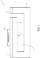
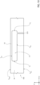
- Figure 1 shows a MEMS device 1 which includes a respective semiconductor body 2, having a cavity 4 extending therewithin. Furthermore, the MEMS device 1 comprises a cantilever 5, which has an end integral with the semiconductor body 2 and includes a respective semiconductive portion 6. An oxide layer 7, which is typically formed by thermal oxide, extends above the semiconductor body 2 and the semiconductive portion 6; furthermore, a transducer 8, which is for example a pressure transducer, extends above the portion of oxide layer 7 that overlies the semiconductive portion 6 and, although not shown, may include, inter alia, a pressure deformable membrane, which is coupled to the cantilever 5 so as to form a corresponding sensing cavity, and corresponding electrodes.
- a transducer 8 which is for example a pressure transducer
- the fact of arranging the transducer 8 above the cantilever 5 allows reducing the impact on the transducer 8 of the residual mechanical stresses which generate during the packaging process of the MEMS device 1 or which generate during the step of soldering the package.
- the cantilever 5 tends to bend downwards, i.e. towards the cavity 4, as qualitatively shown in Figure 1 .
- This deformation of the cantilever 5 is undesired, since it may cause generation of an offset in the transducer 8 and may also lead the non-constrained end of the cantilever 5 to contact the bottom of the cavity 4, in which case the (undesired) stiction of the non-constrained end of the cantilever 5 to the bottom of the cavity 4 may occur.
- the deformation of the cantilever 5 and the resulting drawbacks may also occur in case, above the semiconductive portion 6 of the cantilever 5, a set of layers is present including at least one layer with compressive behavior, not necessarily in direct contact with the semiconductive portion 6 of the cantilever 5.
- WO 2010/061364 A2 discloses a MEMS device according to the preamble of claim 1.
- the aim of the present invention is therefore to provide a MEMS device which at least partially overcomes the drawbacks of the prior art.
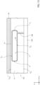
- Figure 2 shows an orthogonal reference system XYZ and a MEMS device 10, which comprises a semiconductor body 12, formed for example by silicon.
- the semiconductor body 12 may comprise for example a semiconductor substrate and one or more epitaxial layers (not shown individually in Figure 2 ). Furthermore, the semiconductor body 12 is delimited upwardly by a front surface S front and is delimited downwardly by a bottom surface S bot . As a first approximation, the front surface S front and the bottom surface S bot are parallel to the XY plane.
- the semiconductor body 12 houses a cavity 13 and forms a fixed semiconductive region 14 and a suspended semiconductive region 16, which extends cantilevered from the fixed semiconductive region 14.
- the fixed semiconductive region 14 delimits the cavity 13 downwardly and laterally; the suspended semiconductive region 16 delimits the cavity 13 upwardly.
- the fixed semiconductive region 14 and the suspended semiconductive region 16 are delimited upwardly by the front surface S front .
- the suspended semiconductive region 16 has a first end, which is fixed to the fixed semiconductive region 14, and a second end, which is free; furthermore, the suspended semiconductive region 16 is delimited downwardly by a first internal surface S in1 , which delimits the cavity 13 upwardly. Furthermore, the cavity 13 is delimited laterally by a lateral surface Si and is delimited downwardly by a second internal surface S in2 , which are formed by the fixed semiconductive region 14.
- the suspended semiconductive region 16 is delimited laterally by a first trench portion 19, which faces, upwardly, the front surface S front and also faces, downwardly, the first internal surface S in1 , so as to communicate with the underlying cavity 13.
- the first trench portion 19 has an elongated shape, for example a 'C' shape, with approximately constant width. Consequently, the first trench portion 19 is delimited laterally by three pairs 17 of lateral walls, which define a lateral trench surface S 19 .
- each pair 17 of lateral walls comprises a respective first wall, formed by the suspended semiconductive region 16, and a respective second wall, formed by the fixed semiconductive region 14 and facing the corresponding first wall, the first and the second walls being approximately parallel to each other and spaced by a distance CD, as visible in Figure 3 , wherein for brevity only the first and the second walls arranged parallel to the XY plane have been indicated (by 18A and 18B, respectively).
- the distance CD is the same for the three pairs 17 of lateral walls and may for example be comprised in the range 0.2 ⁇ m - 2 ⁇ m (boundaries included); however, the distance CD may also be variable according to the pair of lateral walls.
- the MEMS device 10 further comprises a front dielectric layer 20, which is formed by thermal oxide and extends above the front surface S front .
- the front dielectric layer 20 includes a first portion 24, which overlies the fixed semiconductive region 14, in direct contact, and a second portion 26, which overlies the suspended semiconductive region 16, in direct contact.
- the first and the second portions 24, 26 are separated by a second trench portion 39, which extends through the front dielectric layer 20 and communicates with the underlying first trench portion 19, forming a single trench therewith; as a first approximation, in top view the second trench portion 39 may have the same 'C' shape as the first trench portion 19, in such a way that the aforementioned trench also has approximatively a 'C' shape.
- the front dielectric layer 20 may have a thickness comprised in the range 0.5pm - 3.2pm (boundaries included).
- the first portion 24 of the front dielectric layer 20 and the fixed semiconductive region 14 form a fixed structure 25; the second portion 26 of the front dielectric layer 20 and the suspended semiconductive region 16 form a suspended structure 27, which is delimited laterally by the first and the second trench portions 19, 39 and extends cantilevered from the fixed structure 25, being fixed thereto, so as to overlay the cavity 13.
- the MEMS device 10 further comprises an internal dielectric layer 30, which conformally coats the cavity 13, therefore coating the cavity 13 without filling it.
- the internal dielectric layer 30 coats the lateral surface S 1 and the first and the second internal surfaces S in1 , S in2 .
- the compensation portion 31 to indicate the portion of the internal dielectric layer 30 which coats the first internal surface S in1 .
- the compensation portion 31 also forms the suspended structure 27; furthermore, the compensation portion 31 is a mechanical tension compensation portion.
- the internal dielectric layer 30 has a thickness equal to half the distance CD.
- the MEMS device 10 comprises a coating region 33, which is formed by thermal oxide and coats the lateral trench surface S 19 , so as to contact upwardly and downwardly, respectively, with the front dielectric layer 20 and the internal dielectric layer 30, forming a single thermal oxide region therewith.
- the MEMS device 10 further comprises a transducer 40, which is arranged above the second portion 26 of the front dielectric layer 20.
- the transducer 40 is a capacitive pressure transducer and, although not shown, includes a respective pressure deformable membrane and respective electrodes, in such a way that, in use, the transducer 40 is configured to generate an electrical signal indicative of pressure.
- the type of transducer is irrelevant for the purposes of the present invention.
- the suspended semiconductive region 16 is interposed between the second portion 26 of the front dielectric layer 20 and the compensation portion 31 of the internal dielectric layer 30, which, as explained, are both formed by thermal oxide and, therefore, have a same compressive behavior. Therefore, since the second portion 26 of the front dielectric layer 20 and the compensation portion 31 of the internal dielectric layer 30 extend on opposite faces of the suspended semiconductive region 16, a compensation of the tensions which act on the suspended semiconductive region 16 is obtained, reducing the deformation of the suspended semiconductive region 16 and, more generally, of the suspended structure 27. In this manner, possible offsets that might affect the transducer 40, in case the suspended structure 27 were bent, are reduced.
- the MEMS device 10 may be manufactured by the manufacturing process described hereinbelow, from a semiconductive wafer 100, which is intended to form the semiconductor body 12 and is delimited by the front surface S front and the bottom surface S bot .
- the cavity 13 is formed, in a per se known manner.
- the cavity 13 is of buried type, therefore it extends at a distance from the front surface S front and from the bottom surface S bot .
- the semiconductive wafer 100 forms the fixed semiconductive region 14 and a temporary semiconductive region 16', which closes the cavity 13 upwardly and is intended to form the suspended semiconductive region 16.
- an etching process (for example, of dry or wet type) is performed, so as to selectively remove a portion of the temporary semiconductive region 16' and form the first trench portion 19, which communicates with the cavity 13 downwardly.
- the remaining portion of the temporary semiconductive region 16' forms the suspended semiconductive region 16.
- Figure 6 refers to an initial step of the thermal oxidation process
- Figure 7 refers to an intermediate step of the thermal oxidation process
- Figure 8 refers to a terminal step of the thermal oxidation process.
- the shape of the first trench portion 19 does not change during the thermal oxidation process, i.e. the changes in the shape of the first trench portion 19 (in particular, the modifications of the lateral walls) caused by this oxidation are neglected.
- the manufacturing process causes the formation of a preliminary layer 130 of thermal oxide, which coats the lateral surface S 1 and the first and the second internal surfaces S in1 , S in2 of the cavity 13, and the front surface S front ; furthermore, the preliminary layer 130 coats the lateral trench surface S 19 , i.e. the pairs 17 of lateral walls of the first trench portion 19, without completely filling the first trench portion 19, i.e. without closing the first trench portion 19, which forms an opening arranged facing the cavity 13.
- the preliminary layer 130 has a substantially uniform thickness, which increases over time.
- the portions of preliminary layer 130 that coat the front surface S front and the pairs 17 of lateral walls of the first trench portion 19 are exposed to the reagent used in the thermal oxidation process, therefore they gradually increase in thickness; furthermore, since the first trench portion 19 is not closed, the reagent may continue to enter the cavity 13, allowing the gradual increase in thickness also of the portions of the preliminary layer 130 that coat the lateral surface S 1 and the first and the second internal surfaces S in1 , S in2 of the cavity 13.
- the thickness of the preliminary layer 130 becomes approximately equal to half the distance CD, it occurs that, as shown in Figure 7 , the portions of preliminary layer 130 that coat the pairs 17 of lateral walls of the first trench portion 19 obstruct the first trench portion 19, sealing the cavity 13. Since the reagent can no longer access the cavity 13, the thermal oxidation process, and therefore the increase in thickness of the preliminary layer 130, stops within the cavity 13, while continues outside, and in particular, above the front surface S front .
- the portions of preliminary layer 130 that coat the lateral surface S 1 and the first and the second internal surfaces S in1 , S in2 of the cavity 13 form the internal dielectric layer 30; the portions of preliminary layer 130 that coat the front surface S front form the front dielectric layer 20; furthermore, the portions of preliminary layer 130 that coat the pairs 17 of lateral walls of the first trench portion 19 form a top closing region 46, which precisely fills the first trench portion 19, sealing it.
- the thermal oxidation process continues, above the front surface S front , with a resulting increase in thickness of the front dielectric layer 20, as shown in Figure 8 .
- the internal dielectric layer 30 does not undergo modifications.
- a dielectric structure 45 of thermal oxide is present, which comprises the front dielectric layer 20, the internal dielectric layer 30 and the top closing region 46. Furthermore, although not previously described, during the thermal oxidation process, a temporary layer 48 of thermal oxide, whose thickness gradually increases over time during the thermal oxidation process, forms below the bottom surface S bot .
- the temporary layer 48 is removed, in a per se known manner.
- the transducer 40 is formed in a per se known manner; forming the transducer 40 may include forming further regions/layers, not shown.
- an etching for example, of wet or dry type is performed, so as to selectively remove a portion of the front dielectric layer 20 (thus forming the second trench portion 39) and an underlying portion of the top closing region 46, thanks to the use of a mask (not shown).
- a mask not shown
- the first and the second portions 24, 26 of the front dielectric layer 20 are defined and the release of the suspended structure 27 is obtained.
- the remaining portion of the top closing region 46 forms the coating region 33.
- variations are possible, wherein the mask is such that the top closing region 46 is entirely removed, so as to expose the pairs 17 of lateral walls of the trench 19; in this case, the etching process is defined by the trench 19.
- the manufacturing process may therefore proceed in a per se known manner, for example by performing dicing operations on the semiconductive wafer 100, which are not further described.
- a hole 219 is formed, as shown in Figure 10 .
- the hole 219 may have a cylindrical section and extends vertically between the second internal surface S in2 and the bottom surface S bot .
- a thermal oxidation process is performed, in the same manner as described with reference to Figures 6-8 , in such a way as to form the internal dielectric layer 30 and a bottom closing region 246, which is formed by thermal oxide and fills the hole 219, so as to seal the cavity 13.
- the thermal oxidation process causes the formation, within the cavity 13 and the hole 219, of a thermal oxide preliminary layer, whose thickness increases over time, up to obstructing the hole 219; the closing of the hole 219 occurs before the end of the thermal oxidation process.
- the thickness of the internal dielectric layer 30 depends on the shape of the hole 219; for example, in case the hole 219 has an invariant section for translations parallel to the Z-axis, the thickness of the internal dielectric layer 30 depends on the shape of the section of the hole 219.
- the formation of the front dielectric layer 20 and the temporary layer 48 also occurs.
- the temporary layer 48 is removed.
- an epitaxial growth of semiconductor material may be carried out from the bottom surface S bot , as shown in Figure 13 .
- a bottom epitaxial region 248 of semiconductor material which allows the thickness of the semiconductive wafer 100 to be increased, if desired, is formed below the bottom surface S bot ; in any case, the bottom epitaxial region 248 is optional.
- the manufacturing process proceeds with the formation of the transducer 40 on a portion of the front dielectric layer 20 that overlies the temporary semiconductive region 16' and a successive etching process, which selectively removes a portion of the top dielectric layer 20, so as to form the second trench portion 39 and expose a part of the temporary semiconductive region 16', as shown in Figure 14 .
- an etching process (for example, of dry or wet type) is performed to selectively remove a portion of the exposed part of the temporary semiconductive region 16', so as to form the first trench portion 19, and a part of the internal dielectric layer 30 that extends below the first trench portion 19, so as to release the suspended structure 27, as shown in Figure 15 .
- the coating region 33 is absent.
- the front dielectric layer 20 may be removed and successively an alternative dielectric layer 220, formed for example of silicon nitride, may be formed above the front surface S front , as shown in Figure 16 .
- the manufacturing process may then proceed as described with reference to Figures 13-15 , but the transducer 40 is formed on the alternative dielectric layer 220, as shown in Figure 17 .
- the alternative dielectric layer 220 has a tensile behavior, therefore it would per se tend to cause the suspended structure 27 to bend upwards.
- the transducer 40 may include one or more respective layers (not shown) with compressive behavior; consequently, the compensation portion 31 of the internal dielectric layer 30 may be sized so as to compensate the overall behavior of the layers present above the suspended semiconductive region 16, including any layers that form the transducer 40 and are not in direct contact with the suspended semiconductive region 16.
- a layer (not shown) formed by a dielectric different from thermal oxide, which may have tensile behavior, may be present.
- the manufacturing process envisages, after forming the cavity 13 of buried type, forming a plurality of holes 319, which extend between the second internal surface S in2 and the bottom surface S bot , as shown in Figure 18 . Pairs of adjacent holes 319 laterally delimit corresponding semiconductive pillars 320.
- a thermal oxidation process is performed, as already described with reference to Figure 11 .
- the internal dielectric layer 30 and a plurality of bottom closing regions 346 are formed.
- Each bottom closing region 346 is formed by thermal oxide and fills a corresponding hole 319.
- the cavity 13 is thus sealed.
- the thermal oxidation process also causes the formation of the front dielectric layer 20 and the temporary layer 48.
- the front dielectric layer 20, the temporary layer 48 and the bottom closing regions 346 are removed.
- the holes 319 are opened again and also extend through the portion of internal dielectric layer 30 that coats the second internal surface S in2 , forming corresponding openings of the cavity 13.
- a thermal treatment is performed in a hydrogen (H 2 ) environment, which causes a redistribution of the material which forms the semiconductive pillars 320, in such a way that the openings of the cavity 13 close and the internal dielectric layer 30 completely coats again the second internal surface S in2 ; furthermore, between the cavity 13 and the bottom surface S bot an additional cavity 333, of buried type, is formed which, purely by way of example, may allow for example a differential-type pressure transduction to be carried out.
- H 2 hydrogen
- the manufacturing process may continue for example as described with reference to Figure 16 , therefore with the formation of the alternative dielectric layer 220 and with the subsequent operations previously described, but without forming the bottom epitaxial region 248. Furthermore, in case (not shown), after the operations shown in Figure 19 , only the temporary layer 48 and the bottom closing regions 346 were removed (i.e., leaving the front dielectric layer 20), the manufacturing process might proceed as described with reference to Figures 14 and 15 .
- the cavity may be formed in a "silicon-on-insulator" structure 400, which includes a top semiconductive substrate 410 and a bottom semiconductive substrate 412, which are formed for example by silicon and are coupled by interposition of an insulating layer 414 of silicon oxide.
- the cavity 413 is delimited upwardly by a part 416' of the top semiconductive substrate 410, which is delimited downwardly by the first internal surface S in1 ; the second internal surface S in2 is formed by the bottom semiconductive substrate 412.
- a top portion of the lateral surface S 1 is formed by the insulating layer 414; a bottom portion of the lateral surface S 1 is formed by the bottom semiconductive substrate 412.
- the manufacturing process may proceed as described with reference to Figures 5-9 ; the part 416' of the top semiconductive substrate 410 performs the function previously performed by the temporary semiconductive region 16'.
- the MEMS device 430 shown in Figure 23 is obtained, wherein the front dielectric layer (indicated again by 20 and traversed by the second trench portion 39) extends on the top semiconductive substrate 410; the first trench portion (indicated again by 19) extends through the top semiconductive substrate 410 and delimits the suspended semiconductive region (here indicated by 416), which is formed by a residual portion of the part 416' of the top semiconductive substrate 410; the internal dielectric layer (indicated again by 30) coats the cavity 413; the compensation portion (indicated again by 31) extends below the suspended semiconductive region 416.
- the suspended structure (here indicated by 427) is formed by the suspended semiconductive region 416, the compensation portion 31 and the portion of front dielectric layer 20 overlying the suspended semiconductive region 416.
- the present solution allows reducing the bending of the suspended structure which extends cantilevered and supports the transducer, resulting in performance improvement of the latter. Furthermore, the present solution allows setting the thickness of the thermal oxide region which extends below the suspended semiconductive region, so as to adapt the compressive action of this thermal oxide region as a function of the composition of the layers that extend above the suspended semiconductive region.
- the compressive layer arranged above the suspended semiconductive region may form part of the transducer or in any case may not be in direct contact with the suspended semiconductive region.
- the present solution is inexpensive and may be easily integrated into a process flow of a known type.
- the transducer may be of any type.
- the transducer may be suitable for being controlled (e.g., electrically controlled) in order to transduce a control signal into a corresponding transduced signal (e.g., an acoustic signal).
- the shapes of the first and the second trench portions 19, 39 may vary with respect to what has been described; more generally, the relationship between the thickness of the internal dielectric layer 30 and the shape of the first trench portion 19 may vary with respect to what has been described.
- the front dielectric layer 20 may be formed by an oxide other than a thermal oxide, such as for example a deposited oxide.
- the number and the type of layers arranged above the suspended semiconductive region may differ with respect to what has been described.
Landscapes
- Engineering & Computer Science (AREA)
- Microelectronics & Electronic Packaging (AREA)
- Computer Hardware Design (AREA)
- Micromachines (AREA)
Abstract
Description
- The present invention relates to a micro-electromechanical (MEMS) device with compensation of the mechanical stress and to the related manufacturing process.
- As is known, nowadays MEMS devices that envisage the presence of a cantilever are very widespread.
- For example,
Figure 1 shows aMEMS device 1 which includes arespective semiconductor body 2, having acavity 4 extending therewithin. Furthermore, theMEMS device 1 comprises acantilever 5, which has an end integral with thesemiconductor body 2 and includes a respectivesemiconductive portion 6. Anoxide layer 7, which is typically formed by thermal oxide, extends above thesemiconductor body 2 and thesemiconductive portion 6; furthermore, atransducer 8, which is for example a pressure transducer, extends above the portion ofoxide layer 7 that overlies thesemiconductive portion 6 and, although not shown, may include, inter alia, a pressure deformable membrane, which is coupled to thecantilever 5 so as to form a corresponding sensing cavity, and corresponding electrodes. - In practice, the fact of arranging the
transducer 8 above thecantilever 5 allows reducing the impact on thetransducer 8 of the residual mechanical stresses which generate during the packaging process of theMEMS device 1 or which generate during the step of soldering the package. However, due to the compressive behavior of theoxide layer 7, thecantilever 5 tends to bend downwards, i.e. towards thecavity 4, as qualitatively shown inFigure 1 . This deformation of thecantilever 5 is undesired, since it may cause generation of an offset in thetransducer 8 and may also lead the non-constrained end of thecantilever 5 to contact the bottom of thecavity 4, in which case the (undesired) stiction of the non-constrained end of thecantilever 5 to the bottom of thecavity 4 may occur. - In general, the deformation of the
cantilever 5 and the resulting drawbacks may also occur in case, above thesemiconductive portion 6 of thecantilever 5, a set of layers is present including at least one layer with compressive behavior, not necessarily in direct contact with thesemiconductive portion 6 of thecantilever 5. -
WO 2010/061364 A2 discloses a MEMS device according to the preamble ofclaim 1. - The aim of the present invention is therefore to provide a MEMS device which at least partially overcomes the drawbacks of the prior art.
- According to the present invention, a MEMS device and a manufacturing process are provided, as defined in the attached claims.
- For a better understanding of the present invention, embodiments thereof are now described, purely by way of nonlimiting example, with reference to the attached drawings, wherein:
-
Figure 1 schematically shows a cross-section of a MEMS device; -
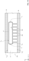
Figure 2 schematically shows a cross-section of an embodiment of the present MEMS device; -
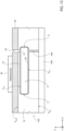
Figure 3 schematically shows a top view with portions removed of the MEMS device shown inFigure 2 ; -
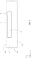
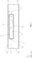
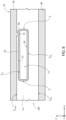
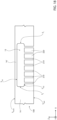
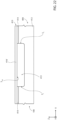
Figures 4-9 schematically show cross-sections of the MEMS device shown inFigure 2 , during successive steps of a manufacturing process; -
Figures 10-15 schematically show cross-sections of a variation of the MEMS device shown inFigure 2 , during successive steps of a manufacturing process; -
Figures 16-17 schematically show cross-sections of a variation of the MEMS device shown inFigure 2 , during successive steps of a manufacturing process; and -
Figures 18-21 schematically show cross-sections of a variation of the MEMS device shown inFigure 2 , during successive steps of a manufacturing process; and -
Figures 22-23 schematically show cross-sections of a variation of the MEMS device shown inFigure 2 , during successive steps of a manufacturing process. -
Figure 2 shows an orthogonal reference system XYZ and aMEMS device 10, which comprises asemiconductor body 12, formed for example by silicon. - In a per se known manner, the
semiconductor body 12 may comprise for example a semiconductor substrate and one or more epitaxial layers (not shown individually inFigure 2 ). Furthermore, thesemiconductor body 12 is delimited upwardly by a front surface Sfront and is delimited downwardly by a bottom surface Sbot. As a first approximation, the front surface Sfront and the bottom surface Sbot are parallel to the XY plane. - The
semiconductor body 12 houses acavity 13 and forms a fixedsemiconductive region 14 and a suspendedsemiconductive region 16, which extends cantilevered from the fixedsemiconductive region 14. In particular, the fixedsemiconductive region 14 delimits thecavity 13 downwardly and laterally; the suspendedsemiconductive region 16 delimits thecavity 13 upwardly. - In greater detail, the fixed
semiconductive region 14 and the suspendedsemiconductive region 16 are delimited upwardly by the front surface Sfront. The suspendedsemiconductive region 16 has a first end, which is fixed to the fixedsemiconductive region 14, and a second end, which is free; furthermore, the suspendedsemiconductive region 16 is delimited downwardly by a first internal surface Sin1, which delimits thecavity 13 upwardly. Furthermore, thecavity 13 is delimited laterally by a lateral surface Si and is delimited downwardly by a second internal surface Sin2, which are formed by the fixedsemiconductive region 14. - In even greater detail, the suspended
semiconductive region 16 is delimited laterally by afirst trench portion 19, which faces, upwardly, the front surface Sfront and also faces, downwardly, the first internal surface Sin1, so as to communicate with theunderlying cavity 13. - As shown in
Figure 3 , wherein thecavity 13 is shown with a dashed line, in top view thefirst trench portion 19 has an elongated shape, for example a 'C' shape, with approximately constant width. Consequently, thefirst trench portion 19 is delimited laterally by threepairs 17 of lateral walls, which define a lateral trench surface S19. In particular, eachpair 17 of lateral walls comprises a respective first wall, formed by the suspendedsemiconductive region 16, and a respective second wall, formed by the fixedsemiconductive region 14 and facing the corresponding first wall, the first and the second walls being approximately parallel to each other and spaced by a distance CD, as visible inFigure 3 , wherein for brevity only the first and the second walls arranged parallel to the XY plane have been indicated (by 18A and 18B, respectively). As a first approximation, the distance CD is the same for the threepairs 17 of lateral walls and may for example be comprised in the range 0.2µm - 2µm (boundaries included); however, the distance CD may also be variable according to the pair of lateral walls. - The
MEMS device 10 further comprises a frontdielectric layer 20, which is formed by thermal oxide and extends above the front surface Sfront. In particular, the frontdielectric layer 20 includes afirst portion 24, which overlies the fixedsemiconductive region 14, in direct contact, and asecond portion 26, which overlies the suspendedsemiconductive region 16, in direct contact. The first and thesecond portions second trench portion 39, which extends through the frontdielectric layer 20 and communicates with the underlyingfirst trench portion 19, forming a single trench therewith; as a first approximation, in top view thesecond trench portion 39 may have the same 'C' shape as thefirst trench portion 19, in such a way that the aforementioned trench also has approximatively a 'C' shape. - Purely by way of example, the front
dielectric layer 20 may have a thickness comprised in the range 0.5pm - 3.2pm (boundaries included). - In practice, the
first portion 24 of the frontdielectric layer 20 and the fixedsemiconductive region 14 form afixed structure 25; thesecond portion 26 of the frontdielectric layer 20 and the suspendedsemiconductive region 16 form a suspendedstructure 27, which is delimited laterally by the first and thesecond trench portions fixed structure 25, being fixed thereto, so as to overlay thecavity 13. - The
MEMS device 10 further comprises an internaldielectric layer 30, which conformally coats thecavity 13, therefore coating thecavity 13 without filling it. In particular, the internaldielectric layer 30 coats the lateral surface S1 and the first and the second internal surfaces Sin1, Sin2. In the following, reference is made to thecompensation portion 31 to indicate the portion of the internaldielectric layer 30 which coats the first internal surface Sin1. Thecompensation portion 31 also forms the suspendedstructure 27; furthermore, thecompensation portion 31 is a mechanical tension compensation portion. - As explained in greater detail below, as a first approximation the internal
dielectric layer 30 has a thickness equal to half the distance CD. - Furthermore, the
MEMS device 10 comprises acoating region 33, which is formed by thermal oxide and coats the lateral trench surface S19, so as to contact upwardly and downwardly, respectively, with the frontdielectric layer 20 and the internaldielectric layer 30, forming a single thermal oxide region therewith. - The
MEMS device 10 further comprises atransducer 40, which is arranged above thesecond portion 26 of the frontdielectric layer 20. - Purely by way of example, the
transducer 40 is a capacitive pressure transducer and, although not shown, includes a respective pressure deformable membrane and respective electrodes, in such a way that, in use, thetransducer 40 is configured to generate an electrical signal indicative of pressure. In any case, the type of transducer is irrelevant for the purposes of the present invention. - In practice, the suspended
semiconductive region 16 is interposed between thesecond portion 26 of the frontdielectric layer 20 and thecompensation portion 31 of the internaldielectric layer 30, which, as explained, are both formed by thermal oxide and, therefore, have a same compressive behavior. Therefore, since thesecond portion 26 of the frontdielectric layer 20 and thecompensation portion 31 of the internaldielectric layer 30 extend on opposite faces of the suspendedsemiconductive region 16, a compensation of the tensions which act on the suspendedsemiconductive region 16 is obtained, reducing the deformation of the suspendedsemiconductive region 16 and, more generally, of the suspendedstructure 27. In this manner, possible offsets that might affect thetransducer 40, in case the suspendedstructure 27 were bent, are reduced. - The
MEMS device 10 may be manufactured by the manufacturing process described hereinbelow, from asemiconductive wafer 100, which is intended to form thesemiconductor body 12 and is delimited by the front surface Sfront and the bottom surface Sbot. - Initially, as shown in
Figure 4 , thecavity 13 is formed, in a per se known manner. In particular, initially thecavity 13 is of buried type, therefore it extends at a distance from the front surface Sfront and from the bottom surface Sbot. In this manner, thesemiconductive wafer 100 forms the fixedsemiconductive region 14 and a temporary semiconductive region 16', which closes thecavity 13 upwardly and is intended to form the suspendedsemiconductive region 16. - Subsequently, as shown in
Figure 5 , an etching process (for example, of dry or wet type) is performed, so as to selectively remove a portion of the temporary semiconductive region 16' and form thefirst trench portion 19, which communicates with thecavity 13 downwardly. The remaining portion of the temporary semiconductive region 16' forms the suspendedsemiconductive region 16. - Successively, as shown in
Figures 6 ,7 and8 , a thermal oxidation process is performed; in particular,Figure 6 refers to an initial step of the thermal oxidation process, whileFigure 7 refers to an intermediate step of the thermal oxidation process;Figure 8 refers to a terminal step of the thermal oxidation process. For simplicity it is assumed that, as a first approximation, the shape of thefirst trench portion 19 does not change during the thermal oxidation process, i.e. the changes in the shape of the first trench portion 19 (in particular, the modifications of the lateral walls) caused by this oxidation are neglected. - In greater detail, as shown in
Figure 6 , initially the manufacturing process causes the formation of apreliminary layer 130 of thermal oxide, which coats the lateral surface S1 and the first and the second internal surfaces Sin1, Sin2 of thecavity 13, and the front surface Sfront; furthermore, thepreliminary layer 130 coats the lateral trench surface S19, i.e. thepairs 17 of lateral walls of thefirst trench portion 19, without completely filling thefirst trench portion 19, i.e. without closing thefirst trench portion 19, which forms an opening arranged facing thecavity 13. Thepreliminary layer 130 has a substantially uniform thickness, which increases over time. In fact, the portions ofpreliminary layer 130 that coat the front surface Sfront and thepairs 17 of lateral walls of thefirst trench portion 19 are exposed to the reagent used in the thermal oxidation process, therefore they gradually increase in thickness; furthermore, since thefirst trench portion 19 is not closed, the reagent may continue to enter thecavity 13, allowing the gradual increase in thickness also of the portions of thepreliminary layer 130 that coat the lateral surface S1 and the first and the second internal surfaces Sin1, Sin2 of thecavity 13. - When the thickness of the
preliminary layer 130 becomes approximately equal to half the distance CD, it occurs that, as shown inFigure 7 , the portions ofpreliminary layer 130 that coat thepairs 17 of lateral walls of thefirst trench portion 19 obstruct thefirst trench portion 19, sealing thecavity 13. Since the reagent can no longer access thecavity 13, the thermal oxidation process, and therefore the increase in thickness of thepreliminary layer 130, stops within thecavity 13, while continues outside, and in particular, above the front surface Sfront. In these conditions, the portions ofpreliminary layer 130 that coat the lateral surface S1 and the first and the second internal surfaces Sin1, Sin2 of thecavity 13 form the internaldielectric layer 30; the portions ofpreliminary layer 130 that coat the front surface Sfront form the frontdielectric layer 20; furthermore, the portions ofpreliminary layer 130 that coat thepairs 17 of lateral walls of thefirst trench portion 19 form atop closing region 46, which precisely fills thefirst trench portion 19, sealing it. - Successively, the thermal oxidation process continues, above the front surface Sfront, with a resulting increase in thickness of the
front dielectric layer 20, as shown inFigure 8 . Conversely, theinternal dielectric layer 30 does not undergo modifications. - In practice, at the end of the thermal oxidation process, a
dielectric structure 45 of thermal oxide is present, which comprises thefront dielectric layer 20, theinternal dielectric layer 30 and thetop closing region 46. Furthermore, although not previously described, during the thermal oxidation process, atemporary layer 48 of thermal oxide, whose thickness gradually increases over time during the thermal oxidation process, forms below the bottom surface Sbot . - Subsequently, as shown in
Figure 9 , thetemporary layer 48 is removed, in a per se known manner. Furthermore, thetransducer 40 is formed in a per se known manner; forming thetransducer 40 may include forming further regions/layers, not shown. - Finally, to obtain the
MEMS device 10 shown inFigure 2 , an etching (for example, of wet or dry type) is performed, so as to selectively remove a portion of the front dielectric layer 20 (thus forming the second trench portion 39) and an underlying portion of thetop closing region 46, thanks to the use of a mask (not shown). In this manner, the first and thesecond portions front dielectric layer 20 are defined and the release of the suspendedstructure 27 is obtained. The remaining portion of thetop closing region 46 forms thecoating region 33. Although not shown, however, variations (not shown) are possible, wherein the mask is such that thetop closing region 46 is entirely removed, so as to expose thepairs 17 of lateral walls of thetrench 19; in this case, the etching process is defined by thetrench 19. - The manufacturing process may therefore proceed in a per se known manner, for example by performing dicing operations on the
semiconductive wafer 100, which are not further described. - According to a variation of the manufacturing process, following the formation of the
cavity 13, of buried type and delimited upwardly by the temporary semiconductive region 16', ahole 219 is formed, as shown inFigure 10 . Purely by way of example, thehole 219 may have a cylindrical section and extends vertically between the second internal surface Sin2 and the bottom surface Sbot. - Subsequently, as shown in
Figure 11 , a thermal oxidation process is performed, in the same manner as described with reference toFigures 6-8 , in such a way as to form theinternal dielectric layer 30 and abottom closing region 246, which is formed by thermal oxide and fills thehole 219, so as to seal thecavity 13. Although not shown in detail, even in this case the thermal oxidation process causes the formation, within thecavity 13 and thehole 219, of a thermal oxide preliminary layer, whose thickness increases over time, up to obstructing thehole 219; the closing of thehole 219 occurs before the end of the thermal oxidation process. Consequently, the thickness of theinternal dielectric layer 30 depends on the shape of thehole 219; for example, in case thehole 219 has an invariant section for translations parallel to the Z-axis, the thickness of theinternal dielectric layer 30 depends on the shape of the section of thehole 219. - During the thermal oxidation process, the formation of the
front dielectric layer 20 and thetemporary layer 48 also occurs. - Subsequently, as shown in
Figure 12 , thetemporary layer 48 is removed. Successively, optionally, an epitaxial growth of semiconductor material may be carried out from the bottom surface Sbot, as shown inFigure 13 . In this manner, abottom epitaxial region 248 of semiconductor material, which allows the thickness of thesemiconductive wafer 100 to be increased, if desired, is formed below the bottom surface Sbot; in any case, thebottom epitaxial region 248 is optional. - Subsequently, the manufacturing process proceeds with the formation of the
transducer 40 on a portion of thefront dielectric layer 20 that overlies the temporary semiconductive region 16' and a successive etching process, which selectively removes a portion of thetop dielectric layer 20, so as to form thesecond trench portion 39 and expose a part of the temporary semiconductive region 16', as shown inFigure 14 . Subsequently, an etching process (for example, of dry or wet type) is performed to selectively remove a portion of the exposed part of the temporary semiconductive region 16', so as to form thefirst trench portion 19, and a part of theinternal dielectric layer 30 that extends below thefirst trench portion 19, so as to release the suspendedstructure 27, as shown inFigure 15 . In this case, thecoating region 33 is absent. - According to a variation, following the operations shown in
Figure 12 , thefront dielectric layer 20 may be removed and successively analternative dielectric layer 220, formed for example of silicon nitride, may be formed above the front surface Sfront, as shown inFigure 16 . In this case, the manufacturing process may then proceed as described with reference toFigures 13-15 , but thetransducer 40 is formed on thealternative dielectric layer 220, as shown inFigure 17 . - The
alternative dielectric layer 220 has a tensile behavior, therefore it would per se tend to cause the suspendedstructure 27 to bend upwards. However, thetransducer 40 may include one or more respective layers (not shown) with compressive behavior; consequently, thecompensation portion 31 of theinternal dielectric layer 30 may be sized so as to compensate the overall behavior of the layers present above the suspendedsemiconductive region 16, including any layers that form thetransducer 40 and are not in direct contact with the suspendedsemiconductive region 16. - In general, even in the case of the manufacturing process described with reference to
Figures 4-9 , in lieu of thefront dielectric layer 20 or above thefront dielectric layer 20, a layer (not shown) formed by a dielectric different from thermal oxide, which may have tensile behavior, may be present. - According to a further variation, the manufacturing process envisages, after forming the
cavity 13 of buried type, forming a plurality ofholes 319, which extend between the second internal surface Sin2 and the bottom surface Sbot, as shown inFigure 18 . Pairs ofadjacent holes 319 laterally delimit correspondingsemiconductive pillars 320. - Subsequently, as shown in
Figure 19 , a thermal oxidation process is performed, as already described with reference toFigure 11 . In this manner, theinternal dielectric layer 30 and a plurality ofbottom closing regions 346 are formed. Eachbottom closing region 346 is formed by thermal oxide and fills acorresponding hole 319. Thecavity 13 is thus sealed. The thermal oxidation process also causes the formation of thefront dielectric layer 20 and thetemporary layer 48. - Subsequently, as shown in
Figure 20 , thefront dielectric layer 20, thetemporary layer 48 and thebottom closing regions 346 are removed. In practice, theholes 319 are opened again and also extend through the portion of internaldielectric layer 30 that coats the second internal surface Sin2, forming corresponding openings of thecavity 13. - Successively, as shown in
Figure 21 , a thermal treatment is performed in a hydrogen (H2) environment, which causes a redistribution of the material which forms thesemiconductive pillars 320, in such a way that the openings of thecavity 13 close and theinternal dielectric layer 30 completely coats again the second internal surface Sin2; furthermore, between thecavity 13 and the bottom surface Sbot anadditional cavity 333, of buried type, is formed which, purely by way of example, may allow for example a differential-type pressure transduction to be carried out. - Subsequently, the manufacturing process may continue for example as described with reference to
Figure 16 , therefore with the formation of thealternative dielectric layer 220 and with the subsequent operations previously described, but without forming thebottom epitaxial region 248. Furthermore, in case (not shown), after the operations shown inFigure 19 , only thetemporary layer 48 and thebottom closing regions 346 were removed (i.e., leaving the front dielectric layer 20), the manufacturing process might proceed as described with reference toFigures 14 and15 . - According to a further variation of the manufacturing process, as shown in
Figure 22 , the cavity (here indicated by 413) may be formed in a "silicon-on-insulator"structure 400, which includes a topsemiconductive substrate 410 and a bottomsemiconductive substrate 412, which are formed for example by silicon and are coupled by interposition of an insulatinglayer 414 of silicon oxide. In this case, thecavity 413 is delimited upwardly by a part 416' of the topsemiconductive substrate 410, which is delimited downwardly by the first internal surface Sin1; the second internal surface Sin2 is formed by the bottomsemiconductive substrate 412. Furthermore, a top portion of the lateral surface S1 is formed by the insulatinglayer 414; a bottom portion of the lateral surface S1 is formed by the bottomsemiconductive substrate 412. - In this case, the manufacturing process may proceed as described with reference to
Figures 5-9 ; the part 416' of the topsemiconductive substrate 410 performs the function previously performed by the temporary semiconductive region 16'. In this manner, theMEMS device 430 shown inFigure 23 is obtained, wherein the front dielectric layer (indicated again by 20 and traversed by the second trench portion 39) extends on the topsemiconductive substrate 410; the first trench portion (indicated again by 19) extends through the topsemiconductive substrate 410 and delimits the suspended semiconductive region (here indicated by 416), which is formed by a residual portion of the part 416' of the topsemiconductive substrate 410; the internal dielectric layer (indicated again by 30) coats thecavity 413; the compensation portion (indicated again by 31) extends below the suspendedsemiconductive region 416. The suspended structure (here indicated by 427) is formed by the suspendedsemiconductive region 416, thecompensation portion 31 and the portion of frontdielectric layer 20 overlying the suspendedsemiconductive region 416. - The advantages that the present solution affords are clear from the preceding description.
- In particular, the present solution allows reducing the bending of the suspended structure which extends cantilevered and supports the transducer, resulting in performance improvement of the latter. Furthermore, the present solution allows setting the thickness of the thermal oxide region which extends below the suspended semiconductive region, so as to adapt the compressive action of this thermal oxide region as a function of the composition of the layers that extend above the suspended semiconductive region. In this regard, as previously mentioned, the compressive layer arranged above the suspended semiconductive region may form part of the transducer or in any case may not be in direct contact with the suspended semiconductive region.
- In addition, the present solution is inexpensive and may be easily integrated into a process flow of a known type.
- Finally, it is clear that modifications and variations may be made to the present MEMS device and the manufacturing process, without departing from the scope of the present invention, as defined in the attached claims.
- For example, in general the transducer may be of any type. Furthermore, the transducer may be suitable for being controlled (e.g., electrically controlled) in order to transduce a control signal into a corresponding transduced signal (e.g., an acoustic signal).
- Furthermore, referring for simplicity to the embodiment shown in
Figure 2 (but the same considerations also apply to the other embodiments), the shapes of the first and thesecond trench portions internal dielectric layer 30 and the shape of thefirst trench portion 19 may vary with respect to what has been described. - As regards the embodiment shown in
Figure 2 , thefront dielectric layer 20 may be formed by an oxide other than a thermal oxide, such as for example a deposited oxide. - Finally, as previously mentioned, the number and the type of layers arranged above the suspended semiconductive region may differ with respect to what has been described.
Claims (13)
- A MEMS device comprising:- a fixed body (14;400) delimiting a cavity (13;413);- a suspended structure (27;427) extending cantilevered from the fixed body, above the cavity, and comprising a suspended semiconductive region (16;416); and- a transducer (40) arranged above the suspended structure;and wherein the suspended structure further comprises a compensation region (31), which extends below the suspended semiconductive region; the MEMS device (10) being characterized in that the compensation region (31) is made of thermal oxide.
- The MEMS device according to claim 1, further comprising at least one compressive region (20) arranged above the suspended semiconductive region (16;416).
- The MEMS device according to claim 2, wherein the compressive region (20) comprises a front dielectric layer (20) of thermal oxide, arranged above the suspended semiconductive region (16;416).
- The MEMS device according to claim 3, wherein the front dielectric layer (20) contacts the suspended semiconductive region (16;416), and wherein the transducer (40) is arranged above the front dielectric layer.
- The MEMS device according to any of the preceding claims, comprising an internal dielectric layer (30) of thermal oxide, which coats the cavity (13) and forms the compensation region (31).
- A process for manufacturing a MEMS device (10;430), comprising:- forming a fixed body (14;400) delimiting a cavity (13;413);- forming a suspended structure (27;427) extending cantilevered from the fixed body, above the cavity, and comprising a suspended semiconductive region (16;416); and- forming a transducer (40) arranged above the suspended structure;and wherein forming the suspended structure comprises forming a compensation region (31), which extends below the suspended semiconductive region; the manufacturing process being characterized in that the compensation region (31) is made of thermal oxide.
- The manufacturing process according to claim 6, comprising forming at least one compressive region (20) arranged above the suspended semiconductive region (16;416).
- The manufacturing process according to claim 7, wherein forming at least one compressive region (20) comprises forming a front dielectric layer (20) of thermal oxide, arranged above the suspended semiconductive region (16; 416) .
- The manufacturing process according to any of claims 6 to 8, wherein forming a fixed body (12) comprises forming a semiconductor body (12) delimited by a front surface (Sfront) and a bottom surface (Sbot) ; said manufacturing process further comprising:- forming the cavity (13) so that it is buried into the semiconductor body;- forming at least one opening (19;219) which extends into the semiconductor body, between the cavity and one of the front surface and the bottom surface; and- performing a thermal oxidation process, so as to coat the cavity with an internal dielectric layer (30) of thermal oxide, which forms the compensation region (31);and wherein forming the suspended structure comprises releasing the suspended structure following the formation of the internal dielectric layer.
- The manufacturing process according to claim 9 when dependent on claim 8, comprising forming the front dielectric layer (20) by said thermal oxidation process.
- The manufacturing process according to claim 9 or 10, comprising, by the thermal oxidation process:- increasing the thickness of the internal dielectric layer (30); and- causing the formation of a closing region (46;246) of thermal oxide which closes the opening (19;219), sealing the cavity (13), so as to stop the increase in thickness of the internal dielectric layer (30) before the end of the thermal oxidation process, in such a way that the thickness of the internal dielectric layer (30) depends on the shape of the opening.
- The manufacturing process according to any of claims 9 to 11, wherein forming at least one opening (19;219) comprises forming, after forming the cavity (13) and before performing the thermal oxidation process, a plurality of openings (319) which extend between the cavity (13) and the bottom surface (Sbot), in such a way that the openings delimit a plurality of pillar semiconductive regions (320); and wherein the execution of the thermal oxidation process causes the formation, in each opening (319), of a corresponding closing region (346) of thermal oxide, so as to seal the cavity; said manufacturing process further comprising:- selectively removing the closing regions; and- performing a thermal treatment so as to cause the formation, from the pillar semiconductive regions (320), of an additional cavity (333), which is of buried type and extends between the cavity and the bottom surface (Sbot).
- The manufacturing process according to any of claims 6 to 8, wherein forming a fixed body (12) comprises forming a structure (400) comprising an insulating layer (414) and a top semiconductive substrate (410) and a bottom semiconductive substrate (412), which are coupled by interposition of the insulating layer; said manufacturing process further comprising:- forming the cavity (413) so that it is delimited upwardly by a part (416') of the top semiconductive substrate and is delimited laterally by portions of the insulating layer and the bottom semiconductive substrate;- forming a trench (19) which extends through the part of the top semiconductive substrate; and- performing a thermal oxidation process, so as to coat the cavity with an internal dielectric layer (30) of thermal oxide, which forms the compensation region (31).
Applications Claiming Priority (1)
| Application Number | Priority Date | Filing Date | Title |
|---|---|---|---|
| IT102023000018465A IT202300018465A1 (en) | 2023-09-08 | 2023-09-08 | MEMS DEVICE WITH MECHANICAL STRESS COMPENSATION AND RELATED MANUFACTURING PROCESS |
Publications (1)
| Publication Number | Publication Date |
|---|---|
| EP4520715A1 true EP4520715A1 (en) | 2025-03-12 |
Family
ID=88690188
Family Applications (1)
| Application Number | Title | Priority Date | Filing Date |
|---|---|---|---|
| EP24195113.6A Pending EP4520715A1 (en) | 2023-09-08 | 2024-08-19 | Mems device with compensation of the mechanical stress and related manufacturing process |
Country Status (2)
| Country | Link |
|---|---|
| EP (1) | EP4520715A1 (en) |
| IT (1) | IT202300018465A1 (en) |
Citations (1)
| Publication number | Priority date | Publication date | Assignee | Title |
|---|---|---|---|---|
| WO2010061364A2 (en) | 2008-11-26 | 2010-06-03 | Freescale Semiconductor, Inc. | Electromechanical transducer device and method of forming a electromechanical transducer device |
-
2023
- 2023-09-08 IT IT102023000018465A patent/IT202300018465A1/en unknown
-
2024
- 2024-08-19 EP EP24195113.6A patent/EP4520715A1/en active Pending
Patent Citations (1)
| Publication number | Priority date | Publication date | Assignee | Title |
|---|---|---|---|---|
| WO2010061364A2 (en) | 2008-11-26 | 2010-06-03 | Freescale Semiconductor, Inc. | Electromechanical transducer device and method of forming a electromechanical transducer device |
Also Published As
| Publication number | Publication date |
|---|---|
| IT202300018465A1 (en) | 2025-03-08 |
Similar Documents
| Publication | Publication Date | Title |
|---|---|---|
| US6913941B2 (en) | SOI polysilicon trench refill perimeter oxide anchor scheme | |
| US6552404B1 (en) | Integratable transducer structure | |
| JP4869943B2 (en) | Micropart with sealed microcavity and method for manufacturing such micropart | |
| US6376291B1 (en) | Process for manufacturing buried channels and cavities in semiconductor material wafers | |
| EP1826174B1 (en) | Method for forming thin film structure having small tensile stress | |
| CN102574676B (en) | Process for manufacturing MEMS devices having buried cavities and MEMS device obtained thereby | |
| US6392158B1 (en) | Structure equipped with electric contacts formed through said structure substrate and method for obtaining said structure | |
| US10800649B2 (en) | Planar processing of suspended microelectromechanical systems (MEMS) devices | |
| US20090181489A1 (en) | Microphone manufacturing method | |
| EP2943766B1 (en) | Structured gap for a mems pressure sensor | |
| US20090206422A1 (en) | Micromechanical diaphragm sensor having a double diaphragm | |
| JPH09129896A (en) | Method for manufacturing monolithic semiconductor device integrated with surface microfabrication structure | |
| TWI848033B (en) | Sensor device and method for producing a sensor device | |
| US20070202628A1 (en) | Manufacturing process for integrated piezo elements | |
| JP2002250665A (en) | Capacitive sensor and method of manufacturing the same | |
| US9458008B1 (en) | Method of making a MEMS die having a MEMS device on a suspended structure | |
| KR20220080415A (en) | MEMS microphone and method of manufacturing the same | |
| CN120081331A (en) | MEMS devices with mechanical stress compensation and related manufacturing processes | |
| US6724058B2 (en) | Method for producing a filled recess in a material layer, and an integrated circuit configuration produced by the method | |
| JPH06302834A (en) | Manufacture of thin-film structure | |
| JP2000088685A (en) | Micro mechanical structure | |
| EP4467951B1 (en) | Capacitive mems pressure transducer and related manufacturing process | |
| IT202300018465A1 (en) | MEMS DEVICE WITH MECHANICAL STRESS COMPENSATION AND RELATED MANUFACTURING PROCESS | |
| US20210387854A1 (en) | Method for Manufacturing an Integrated MEMS Transducer Device and Integrated MEMS Transducer Device | |
| US20260118197A1 (en) | Pressure sensor having high detection performance and optimized manufacturing |
Legal Events
| Date | Code | Title | Description |
|---|---|---|---|
| PUAI | Public reference made under article 153(3) epc to a published international application that has entered the european phase |
Free format text: ORIGINAL CODE: 0009012 |
|
| STAA | Information on the status of an ep patent application or granted ep patent |
Free format text: STATUS: THE APPLICATION HAS BEEN PUBLISHED |
|
| AK | Designated contracting states |
Kind code of ref document: A1 Designated state(s): AL AT BE BG CH CY CZ DE DK EE ES FI FR GB GR HR HU IE IS IT LI LT LU LV MC ME MK MT NL NO PL PT RO RS SE SI SK SM TR |
|
| STAA | Information on the status of an ep patent application or granted ep patent |
Free format text: STATUS: REQUEST FOR EXAMINATION WAS MADE |
|
| 17P | Request for examination filed |
Effective date: 20250825 |
|
| REG | Reference to a national code |
Ref country code: DE Ref legal event code: R079 Free format text: PREVIOUS MAIN CLASS: B81B0003000000 Ipc: B81B0007000000 Ref country code: DE Ref legal event code: R079 Ref document number: 602024005079 Country of ref document: DE Free format text: PREVIOUS MAIN CLASS: B81B0003000000 Ipc: B81B0007000000 |
|
| GRAP | Despatch of communication of intention to grant a patent |
Free format text: ORIGINAL CODE: EPIDOSNIGR1 |
|
| STAA | Information on the status of an ep patent application or granted ep patent |
Free format text: STATUS: GRANT OF PATENT IS INTENDED |
|
| RIC1 | Information provided on ipc code assigned before grant |
Ipc: B81B 7/00 20060101AFI20251127BHEP |
|
| INTG | Intention to grant announced |
Effective date: 20251222 |
|
| GRAS | Grant fee paid |
Free format text: ORIGINAL CODE: EPIDOSNIGR3 |
|
| GRAA | (expected) grant |
Free format text: ORIGINAL CODE: 0009210 |
|
| STAA | Information on the status of an ep patent application or granted ep patent |
Free format text: STATUS: THE PATENT HAS BEEN GRANTED |