EP4520599A1 - Battery system and power transmission method using same - Google Patents
Battery system and power transmission method using same Download PDFInfo
- Publication number
- EP4520599A1 EP4520599A1 EP23903708.8A EP23903708A EP4520599A1 EP 4520599 A1 EP4520599 A1 EP 4520599A1 EP 23903708 A EP23903708 A EP 23903708A EP 4520599 A1 EP4520599 A1 EP 4520599A1
- Authority
- EP
- European Patent Office
- Prior art keywords
- voltage
- level
- wiring
- auxiliary
- power path
- Prior art date
- Legal status (The legal status is an assumption and is not a legal conclusion. Google has not performed a legal analysis and makes no representation as to the accuracy of the status listed.)
- Pending
Links
Images


Classifications
-
- B—PERFORMING OPERATIONS; TRANSPORTING
- B60—VEHICLES IN GENERAL
- B60R—VEHICLES, VEHICLE FITTINGS, OR VEHICLE PARTS, NOT OTHERWISE PROVIDED FOR
- B60R16/00—Electric or fluid circuits specially adapted for vehicles and not otherwise provided for; Arrangement of elements of electric or fluid circuits specially adapted for vehicles and not otherwise provided for
- B60R16/02—Electric or fluid circuits specially adapted for vehicles and not otherwise provided for; Arrangement of elements of electric or fluid circuits specially adapted for vehicles and not otherwise provided for electric constitutive elements
- B60R16/03—Electric or fluid circuits specially adapted for vehicles and not otherwise provided for; Arrangement of elements of electric or fluid circuits specially adapted for vehicles and not otherwise provided for electric constitutive elements for supply of electrical power to vehicle subsystems or for
- B60R16/033—Electric or fluid circuits specially adapted for vehicles and not otherwise provided for; Arrangement of elements of electric or fluid circuits specially adapted for vehicles and not otherwise provided for electric constitutive elements for supply of electrical power to vehicle subsystems or for characterised by the use of electrical cells or batteries
-
- B—PERFORMING OPERATIONS; TRANSPORTING
- B60—VEHICLES IN GENERAL
- B60R—VEHICLES, VEHICLE FITTINGS, OR VEHICLE PARTS, NOT OTHERWISE PROVIDED FOR
- B60R16/00—Electric or fluid circuits specially adapted for vehicles and not otherwise provided for; Arrangement of elements of electric or fluid circuits specially adapted for vehicles and not otherwise provided for
- B60R16/02—Electric or fluid circuits specially adapted for vehicles and not otherwise provided for; Arrangement of elements of electric or fluid circuits specially adapted for vehicles and not otherwise provided for electric constitutive elements
- B60R16/023—Electric or fluid circuits specially adapted for vehicles and not otherwise provided for; Arrangement of elements of electric or fluid circuits specially adapted for vehicles and not otherwise provided for electric constitutive elements for transmission of signals between vehicle parts or subsystems
-
- H—ELECTRICITY
- H02—GENERATION; CONVERSION OR DISTRIBUTION OF ELECTRIC POWER
- H02J—ELECTRIC POWER NETWORKS; CIRCUIT ARRANGEMENTS OR SYSTEMS FOR SUPPLYING OR DISTRIBUTING ELECTRIC POWER; SYSTEMS FOR STORING ELECTRIC ENERGY
- H02J1/00—Circuit arrangements for DC mains or DC distribution networks
- H02J1/06—Two-wire DC power distribution systems
-
- H—ELECTRICITY
- H02—GENERATION; CONVERSION OR DISTRIBUTION OF ELECTRIC POWER
- H02J—ELECTRIC POWER NETWORKS; CIRCUIT ARRANGEMENTS OR SYSTEMS FOR SUPPLYING OR DISTRIBUTING ELECTRIC POWER; SYSTEMS FOR STORING ELECTRIC ENERGY
- H02J1/00—Circuit arrangements for DC mains or DC distribution networks
- H02J1/08—Three-wire DC power distribution systems; Systems having more than three wires
- H02J1/084—Three-wire DC power distribution systems; Systems having more than three wires for selectively connecting the load or loads to one or several among a plurality of power lines or power sources
-
- H—ELECTRICITY
- H02—GENERATION; CONVERSION OR DISTRIBUTION OF ELECTRIC POWER
- H02J—ELECTRIC POWER NETWORKS; CIRCUIT ARRANGEMENTS OR SYSTEMS FOR SUPPLYING OR DISTRIBUTING ELECTRIC POWER; SYSTEMS FOR STORING ELECTRIC ENERGY
- H02J7/00—Circuit arrangements for charging or discharging batteries or for supplying loads from batteries
-
- H—ELECTRICITY
- H02—GENERATION; CONVERSION OR DISTRIBUTION OF ELECTRIC POWER
- H02M—APPARATUS FOR CONVERSION BETWEEN AC AND AC, BETWEEN AC AND DC, OR BETWEEN DC AND DC, AND FOR USE WITH MAINS OR SIMILAR POWER SUPPLY SYSTEMS; CONVERSION OF DC OR AC INPUT POWER INTO SURGE OUTPUT POWER; CONTROL OR REGULATION THEREOF
- H02M3/00—Conversion of DC power input into DC power output
- H02M3/02—Conversion of DC power input into DC power output without intermediate conversion into AC
- H02M3/04—Conversion of DC power input into DC power output without intermediate conversion into AC by static converters
- H02M3/10—Conversion of DC power input into DC power output without intermediate conversion into AC by static converters using discharge tubes with control electrode or semiconductor devices with control electrode
- H02M3/145—Conversion of DC power input into DC power output without intermediate conversion into AC by static converters using discharge tubes with control electrode or semiconductor devices with control electrode using devices of a triode or transistor type requiring continuous application of a control signal
- H02M3/155—Conversion of DC power input into DC power output without intermediate conversion into AC by static converters using discharge tubes with control electrode or semiconductor devices with control electrode using devices of a triode or transistor type requiring continuous application of a control signal using semiconductor devices only
- H02M3/156—Conversion of DC power input into DC power output without intermediate conversion into AC by static converters using discharge tubes with control electrode or semiconductor devices with control electrode using devices of a triode or transistor type requiring continuous application of a control signal using semiconductor devices only with automatic control of output voltage or current, e.g. switching regulators
- H02M3/158—Conversion of DC power input into DC power output without intermediate conversion into AC by static converters using discharge tubes with control electrode or semiconductor devices with control electrode using devices of a triode or transistor type requiring continuous application of a control signal using semiconductor devices only with automatic control of output voltage or current, e.g. switching regulators including plural semiconductor devices as final control devices for a single load
- H02M3/1582—Buck-boost converters
-
- H—ELECTRICITY
- H03—ELECTRONIC CIRCUITRY
- H03M—CODING; DECODING; CODE CONVERSION IN GENERAL
- H03M1/00—Analogue/digital conversion; Digital/analogue conversion
- H03M1/12—Analogue/digital converters
-
- B—PERFORMING OPERATIONS; TRANSPORTING
- B60—VEHICLES IN GENERAL
- B60Y—INDEXING SCHEME RELATING TO ASPECTS CROSS-CUTTING VEHICLE TECHNOLOGY
- B60Y2400/00—Special features of vehicle units
- B60Y2400/11—Electric energy storages
- B60Y2400/112—Batteries
-
- H—ELECTRICITY
- H02—GENERATION; CONVERSION OR DISTRIBUTION OF ELECTRIC POWER
- H02J—ELECTRIC POWER NETWORKS; CIRCUIT ARRANGEMENTS OR SYSTEMS FOR SUPPLYING OR DISTRIBUTING ELECTRIC POWER; SYSTEMS FOR STORING ELECTRIC ENERGY
- H02J2105/00—Networks for supplying or distributing electric power characterised by their spatial reach or by the load
- H02J2105/30—Networks for supplying or distributing electric power characterised by their spatial reach or by the load the load networks being external to vehicles, i.e. exchanging power with vehicles
Definitions
- the present disclosure relates to a battery system and a power delivery method using the same.
- a voltage supplied from an auxiliary (AUX) terminal of a vehicle may be 12 V or 24 V.
- a conventional battery system may be classified into a system corresponding to 12V and a system corresponding to 24V.
- a separate element may be provided in a path based on each voltage level in order to perform the classification into the systems corresponding to each voltage level as described above. Accordingly, a battery management system (BMS) including the element for each voltage level may have a large number of elements, which may cause an insufficient space on a board or require a board for each voltage level.
- BMS battery management system
- the present disclosure attempts to provide a battery system for determining a power path through which a voltage is delivered to various elements based on a level of the voltage input from an auxiliary (AUX) terminal, and a power delivery method using the same.
- AUX auxiliary
- a battery system including: a battery pack; and a battery management system (BMS) receiving an auxiliary voltage from an auxiliary (AUX) line, selecting one of a first power path and a second power path from the auxiliary voltage to a plurality of driving elements based on a level of the auxiliary voltage, and supplying power to the plurality of driving elements through the selected one power path, wherein the BMS includes a first wiring configuring the first power path, a second wiring configuring the second power path a switching element including a first end to which the auxiliary voltage is provided, a second end which is connected to the first wiring, and a third end which is connected to the second wiring, and a buck-boost element stepping down the voltage supplied through the second wiring.
- BMS battery management system
- the BMS further may include a main control unit (MCU) generating a switch control signal based on a signal indicating a noise-filtered voltage from the auxiliary voltage, and the switching element may connect the first end to the second end or the third end based on the switch control signal.
- MCU main control unit
- the BMS may further include an analog-digital converter (ADC) analog-digital converting the filtered voltage to generate a voltage signal indicating a level of the filtered voltage, and transmitting the generated signal to the MCU.
- ADC analog-digital converter
- the selecting of the one of the first power path and the second power path may include analog-to-digital converting a noise-filtered voltage from the auxiliary voltage to generate a voltage signal indicating a level of the noise-filtered voltage; and generating a switch control signal based on the voltage signal.
- the method in which the switch control signal has a second level when the noise-filtered voltage has a level corresponding to a second voltage, may further include connecting, by the switching element, the third end to the first end based on the switch control signa.
- the ADC 202 may generate a voltage signal VS by analog-to-digital converting a signal indicating the voltage at the node N_FT.
- the voltage signal VS may be a signal indicating a level of the voltage output from the input filter 201.
- the SBC 208 may supply power to the MCU 209.
- the SBC 208 may generate a driving voltage 5V_PWR of the MCU 209 and supply the same to the MCU 209.
- a first wiring LN1 may be a wiring that provides the power path from an output of the input filter 201 to a node N1 connected to one end of each of the plurality of driving elements 205 to 208.
- One end of the first wiring LN1 may be connected to the second end N_SW2 of the switching element 203, and the other end of the first wiring LN1 may be connected to the node N1.
- a second wiring LN2 may be a wiring that provides the power path from the output of the input filter 201 to the buck-boost element 204.
- One end of the second wiring LN2 may be connected to the third end N_SW3 of the switching element 203, and the other end of the second wiring LN2 may be connected to one end of the buck-boost element 204.
- the MCU 209 may generate a switch control signal CTR_SW based on the voltage signal VS received from the node N_FT through the ADC 202.
- the MCU 209 may select the power path from the first auxiliary voltage V1 or the second auxiliary voltage V2 to the plurality of driving elements 205 to 208 through the switch control signal CTR_SW.
- the MCU 209 may select one of a first power path configured by the first wiring LN1 and a second power path configured by the second wiring LN2.
- the MCU 209 may generate the switch control signal CTR_SW of a first level when the voltage signal VS has a level corresponding to the first auxiliary voltage V1.
- the MCU 209 may generate the switch control signal CTR_SW of a second level when the voltage signal VS has a level corresponding to the second auxiliary voltage V2.
- the switching element 203 may connect the output line LN_FT of the input filter 201 to the first wiring LN1.
- the switching element 203 may connect the output line LN_FT of the input filter 201 to the second wiring LN2.
- the BMS 200 may supply power to the plurality of driving elements 205 to 208 through one power path selected from the first power path configured by the first wiring LN1 and the second power path configured by the second wiring LN2.
- a configuration of the buck-boost element 204 and step-up and step-down methods of the buck-boost element 204 are not particularly limited.
- the buck-boost element 204 may be operated when the voltage corresponding to the second auxiliary voltage V2 is supplied thereto through the second wiring.
- the buck-boost element 204 may output the voltage of the level corresponding to the first auxiliary voltage by stepping down the voltage input through the second wiring LN2.
- the other end of the buck-boost element 204 may be connected to the wirings connected to the plurality of driving elements 205 to 208 through the node N1.
- Power may be supplied to the plurality of driving elements 205 to 208 through the first wiring LN1 or the buck-boost element 204.
- the main relay driver 205 may use a voltage of power supplied through the node N1 as its driving voltage.
- the main relay driver may generate the main relay driving voltage V_REL by using the voltage of power supplied through the node N1, and close the main relay 300 by providing the main relay driving voltage V_REL to the main relay 300.
- the precharge relay driver 206 may use power supplied through the node N1 as its driving voltage.
- the precharge relay driver may generate the precharge relay driving voltage V_PRE by using the voltage of power supplied through the node N1, and close the precharge relay 310 by providing the precharge relay driving voltage V_PRE to the precharge relay 310.
- the current sensor regulator 207 may supply the driving voltage V_CS required for operating the current sensor 400 by converting the voltage of power supplied through the node N1 to a voltage of a level suitable for the current sensor 400.
- the SBC 208 may generate the voltage of 5V_PWR based on power supplied through the node N1 and supply the same to the MCU 209.
- FIG. 1 shows one node N1.
- the BMS 200 may include two or more nodes connected to the first wiring LN1 and the other end of the buck-boost element 204, and the plurality of driving elements 205 to 208 may be connected to the first wiring or the other end of buck-boost element 204 through two or more nodes.
- the battery system 1 may be connected to the external device 2.
- the external device 2 may include a loading or charging device such as an inverter or a converter.
- a loading or charging device such as an inverter or a converter.
- both the ends P+ and P- of the battery system 1 may be connected to the charger and supplied with power from the charger to be charged.
- both the ends P+ and P- of the battery system 1 may be connected to the load, and power supplied by the battery pack 100 may thus be discharged through the load.
- FIG. 2 shows the power path when the first auxiliary voltage is supplied from an auxiliary (AUX) line.
- the input filter 201 may deliver a noise-filtered voltage from the first auxiliary voltage V1 to the switching element 203 through the output line LN_FT.
- the ADC 202 may transmit, to the MCU 209, the voltage signal VS which is a digital conversion of the voltage at the node N_FT on the output line LN_FT.
- the voltage signal VS may have the level corresponding to the first auxiliary voltage V1, and the MCU 209 may thus generate the switch control signal CTR_SW of the first level and transmit the same to the switching element 203.
- the switching element 203 receiving the switch control signal CTR_SW of the first level may connect the first end N_SW1 with the second end N_SW2 to thus connect the output line LN_FT of the input filter 201 to the first wiring LN1.
- the first wiring LN1 may be connected to the wirings connected to the plurality of driving elements 205 to 208 through the node N1.
- the first auxiliary voltage V1 supplied to the AUX line may be supplied to the plurality of driving elements 205 to 208 through the output line LN_FT of the input filter 201, the first wiring LN1, and the node N1.
- FIG. 3 shows the power path when the second auxiliary voltage is supplied from the AUX line.
- the input filter 201 may deliver the noise-filtered voltage from the second auxiliary voltage V2 to the switching element 203 through the output line LN_FT.
- the ADC 202 may transmit, to the MCU 209, the voltage signal VS which is the digital conversion of the voltage at the node N_FT on the output line LN_FT.
- the voltage signal VS may have the level corresponding to the second auxiliary voltage V2, and the MCU 209 may thus generate the switch control signal CTR_SW of the second level and transmit the same to the switching element 203.
- the switching element 203 receiving the switch control signal CTR_SW of the second level may connect the first end N_SW1 with the third end N_SW3 to thus connect the output line LN_FT of the input filter 201 to the second wiring LN2.
- the second wiring LN2 may be connected to the buck-boost element 204.
- the MCU 209 may receive the voltage signal VS from the ADC 202 to determine whether the voltage signal VS has a level corresponding to the first auxiliary voltage V1 or that of the second auxiliary voltage V2 (S400).
- the switching element 203 receiving the switch control signal of the second level may connect the first end N_SW1 with a third end N_SW3, and deliver power to a buck-boost element 204 through a second wiring LN2 (S800).
- the output voltage of the buck-boost element 204 may be delivered to the plurality of driving elements 205 to 208 (S1000).
- the plurality of driving elements 205 to 208 may be driven using the output voltage of the buck-boost element 204 as the driving voltage.
Landscapes
- Engineering & Computer Science (AREA)
- Power Engineering (AREA)
- Mechanical Engineering (AREA)
- Theoretical Computer Science (AREA)
- Charge And Discharge Circuits For Batteries Or The Like (AREA)
- Direct Current Feeding And Distribution (AREA)
- Dc-Dc Converters (AREA)
Abstract
Description
- This application claims the benefit of priority based on
Korean Patent Application No. 10-2022-0177519 filed in the Korean Intellectual Property Office on December 16, 2022 - The present disclosure relates to a battery system and a power delivery method using the same.
- A voltage supplied from an auxiliary (AUX) terminal of a vehicle may be 12 V or 24 V. A conventional battery system may be classified into a system corresponding to 12V and a system corresponding to 24V.
- A separate element may be provided in a path based on each voltage level in order to perform the classification into the systems corresponding to each voltage level as described above. Accordingly, a battery management system (BMS) including the element for each voltage level may have a large number of elements, which may cause an insufficient space on a board or require a board for each voltage level.
- The present disclosure attempts to provide a battery system for determining a power path through which a voltage is delivered to various elements based on a level of the voltage input from an auxiliary (AUX) terminal, and a power delivery method using the same.
- According to an embodiment, provided is a battery system including:
a battery pack; and a battery management system (BMS) receiving an auxiliary voltage from an auxiliary (AUX) line, selecting one of a first power path and a second power path from the auxiliary voltage to a plurality of driving elements based on a level of the auxiliary voltage, and supplying power to the plurality of driving elements through the selected one power path, wherein the BMS includes a first wiring configuring the first power path, a second wiring configuring the second power path a switching element including a first end to which the auxiliary voltage is provided, a second end which is connected to the first wiring, and a third end which is connected to the second wiring, and a buck-boost element stepping down the voltage supplied through the second wiring. - The BMS further may include a main control unit (MCU) generating a switch control signal based on a signal indicating a noise-filtered voltage from the auxiliary voltage, and the switching element may connect the first end to the second end or the third end based on the switch control signal.
- The BMS may further include an analog-digital converter (ADC) analog-digital converting the filtered voltage to generate a voltage signal indicating a level of the filtered voltage, and transmitting the generated signal to the MCU.
- Each of the plurality of driving elements is driven at a voltage level of a first voltage, the MCU may generate the switch control signal of a first level when the noise-filtered voltage has a level corresponding to the first voltage, and the switching element connectsthe second end to the first end.
- The MCU may generate the switch control signal of a second level when the noise-filtered voltage has a level corresponding to a second voltage, the switching element connects the third end to the first end, and the buck-boost element may output the voltage of the level corresponding to the first voltage by stepping down the voltage supplied through the second wiring, and supply the outputed voltage to the plurality of driving elements.
- According to another embodiment, provided is a power delivery method including: receiving, by a battery management system (BMS), an auxiliary voltage from an auxiliary (AUX) line of a vehicle; selecting, by the BMS, one of a first power path and a second power path from the auxiliary voltage to a plurality of driving elements driven at a voltage level of a first voltage based on a level of the auxiliary voltage; connecting, by the BMS, a first end to a second end or a third end based on the selection by using a switching element including the first end to which the auxiliary voltage is provided, the second end which is connected to a first wiring configuring the first power path, and the third end which is connected to a second wiring configuring the second power path; and supplying power to the plurality of driving elements through the selected one power path.
- The selecting of the one of the first power path and the second power path may include analog-to-digital converting a noise-filtered voltage from the auxiliary voltage to generate a voltage signal indicating a level of the noise-filtered voltage; and generating a switch control signal based on the voltage signal.
- The method, in which the switch control signal has a first level when the noise-filtered voltage has a level corresponding to the first voltage, may further include connecting, by the switching element, the second end to the first end based on the switch control signal.
- The method, in which the switch control signal has a second level when the noise-filtered voltage has a level corresponding to a second voltage, may further include connecting, by the switching element, the third end to the first end based on the switch control signa.
- The method may further include: outputting, by the buck-boost element, the voltage of the level corresponding to the first voltage by stepping down the voltage supplied through the second wiring; and supplying, by the buck-boost element, the outputed voltage to the plurality of driving elements.
- According to the present disclosure, the 12 V and 24 V systems may be implemented as one battery management system (BMS) mounted on one board, and the 12V system and the 24V system may thus be flexibly utilized only by managing a bill of materials (BOM).
- According to the present disclosure, both of the 12 V and 24 V systems may be designed using one board, and the BMS may thus be designed regardless of the 12 V or 24 V AUX system provided by the vehicle terminal.
-
-
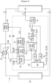
FIG. 1 is a block diagram schematically showing a battery system according to an embodiment. -
FIG. 2 shows a power path when a first auxiliary voltage is supplied from an auxiliary (AUX) line. -
FIG. 3 shows the power path when a second auxiliary voltage is supplied from the auxiliary (AUX) line. -
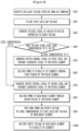
FIG. 4 is a flowchart of a power delivery method using a battery system according to another embodiment. - Hereinafter, embodiments disclosed in the specification are described in detail with reference to the accompanying drawings, the same or similar components are denoted by the same or similar reference numerals, and an overlapping description thereof is omitted. Terms "module" and/or "unit" for components described in the following description are used only to make the specification easily understood. Therefore, these terms do not have meanings or roles distinguished from each other in themselves. Further, in describing the embodiments of the present disclosure, omitted is a detailed description when it is decided that the detailed description of the known art related to the present disclosure may obscure the gist. Furthermore, it is to be understood that the accompanying drawings are provided only to allow the embodiment of the present disclosure to be easily understood, and the spirit of the present disclosure is not limited by the accompanying drawings and includes all the modifications, equivalents and substitutions included in the spirit and scope of the present disclosure.
- Terms including ordinal numbers such as "first," "second" and the like, may be used to describe various components. However, these components are not limited by these terms. The terms are used only to distinguish one component from another component.
- It is to be understood that terms "include," "have" and the like used in the present application specify the presence of features, numerals, steps, operations, components, parts or combinations thereof, mentioned in the specification, and do not preclude the presence or possible addition of one or more other features, numerals, steps, operations, components, parts or combinations thereof.
- A program implemented as a set of instructions embodying a control algorithm necessary to control another configuration may be installed in a configuration for controlling another configuration under a specific control condition among configurations according to an embodiment. The control configuration may process input data and stored data, based on the installed program to thus generate output data. The control configuration may include a non-volatile memory that stores the program and a memory that stores the data.
-
FIG. 1 is a block diagram schematically showing a battery system according to an embodiment. - Referring to
FIG. 1 , abattery system 1 may include abattery pack 100, a battery management system (BMS) 200, amain relay 300, aprecharge relay 310, and acurrent sensor 400. - The
battery pack 100 may be implemented as two or more battery cells connected in series with each other, a plurality of battery cells connected in series with each other in which two or more battery cells are connected in parallel with each other, or two or more battery cells connected in parallel with each other. - One end of the
precharge relay 310 may be connected to one end of themain relay 300, and the other end of theprecharge relay 310 may be connected to the other end of themain relay 300. One end of each of themain relay 300 and theprecharge relay 310 may be connected to thebattery pack 100, and the other end of each of themain relay 300 and theprecharge relay 310 may be connected to at least one component of an external device 2. - The BMS 200 may include an
input filter 201, an analog-digital converter (ADC) 202, aswitching element 203, a buck-boost element 204, and a plurality ofdriving elements 205 to 208, and a main control unit (MCU) 209. The plurality ofdriving elements 205 to 208 are respective examples of elements operated to control charging and discharging of thebattery pack 100. - The
BMS 200 may receive an auxiliary voltage from an auxiliary (AUX) line, determine a power path for connecting the auxiliary voltage to the plurality ofdriving elements 205 to 208 based on a level of the auxiliary voltage, and supply power to the plurality ofdriving elements 205 to 208 through a wiring of the power path. - The BMS 200 may include at least one AUX line. For example, the auxiliary voltage of a vehicle may be supplied through the AUX line. Hereinafter, for convenience of explanation, the description describes that one of a first auxiliary voltage V1 and a second auxiliary voltage V2 is supplied through the AUX line. The second auxiliary voltage V2 may be higher than the first auxiliary voltage V1. For example, the first auxiliary voltage V1 may be 12 V and the second auxiliary voltage V2 may be 24 V.
- The
input filter 201 may filter the voltage supplied from the AUX line. One end of theinput filter 201 may be connected to the AUX line, and the other end of theinput filter 201 may be connected to one end of theswitching element 203 through an output line LN_FT. Theinput filter 201 may be implemented as an inductor or a capacitor, and any of various known noise removal filters may be applied to theinput filter 201. The voltage passed through theinput filter 201 may be delivered to theswitching element 203 through the output line LN_FT. The output line LN_FT may be a wiring that provides the power path from an output terminal of theinput filter 201 to one end of theswitching element 203. - One end of the
ADC 202 may be connected to a node N_FT on the output line LN_FT, and the other end of theADC 202 may be connected to theMCU 209. TheADC 202 may generate a voltage signal VS by analog-to-digital converting a signal indicating the voltage at the node N_FT. The voltage signal VS may be a signal indicating a level of the voltage output from theinput filter 201. - The plurality of
driving elements 205 to 208 may include at least one of amain relay driver 205, aprecharge relay driver 206, acurrent sensor regulator 207, and a system basis chip (SBC) 208. A voltage level of power required for operating the plurality ofdriving elements 205 to 208 may be a voltage level of the first auxiliary voltage V1.FIG. 1 shows that the plurality of driving elements are themain relay driver 205, theprecharge relay driver 206, thecurrent sensor regulator 207, and theSBC 208. However, the present disclosure is not limited thereto. For example, the plurality of driving elements may include a high voltage interlock connector (HVIL). - The
main relay driver 205 may control driving of themain relay 300. Opening and closing of themain relay 300 may be controlled by a main relay control signal CTR_REL supplied from theMCU 209. Themain relay driver 205 may supply a main relay driving voltage V_REL to themain relay 300 which opens or closes themain relay 300 based the main relay control signal CTR_REL. - The
precharge relay driver 206 may control driving of theprecharge relay 310. The opening and closing of theprecharge relay 310 may be controlled by a precharge relay control signal CTR_PRE supplied from theMCU 209. Theprecharge relay driver 206 may supply a precharge relay driving voltage V_PRE to theprecharge relay 310 which opens or closes theprecharge relay 310 based on the precharge relay control signal CTR_PRE. - The
current sensor regulator 207 may supply a driving voltage V_CS to thecurrent sensor 400 which measures a current flowing in a high voltage path to which thebattery pack 100 is connected. Thecurrent sensor 400 may be disposed on a high voltage line connected from thebattery pack 100 to both ends P+ and P- of thebattery system 1. For example, when an excessive current flows in the high voltage path, a circuit phenomenon may occur in the pack, and theMCU 209 may detect this phenomenon by monitoring current information acquired by thecurrent sensor 400. Thecurrent sensor 400 may be implemented as a resistance detection type sensor that detects the current by using a resistance or a magnetic field detection type sensor that detects a magnetic field. - The
SBC 208 may supply power to theMCU 209. TheSBC 208 may generate a driving voltage 5V_PWR of theMCU 209 and supply the same to theMCU 209. - The switching
element 203 may include a first end N_SW1, a second end N_SW2, and a third end N_SW3. - The first end N_SW1 of the
switching element 203 may be connected to the node N_FT through the output line LN_FT. - A first wiring LN1 may be a wiring that provides the power path from an output of the
input filter 201 to a node N1 connected to one end of each of the plurality of drivingelements 205 to 208. One end of the first wiring LN1 may be connected to the second end N_SW2 of theswitching element 203, and the other end of the first wiring LN1 may be connected to the node N1. - A second wiring LN2 may be a wiring that provides the power path from the output of the
input filter 201 to the buck-boost element 204. One end of the second wiring LN2 may be connected to the third end N_SW3 of theswitching element 203, and the other end of the second wiring LN2 may be connected to one end of the buck-boost element 204. - The
MCU 209 may generate a switch control signal CTR_SW based on the voltage signal VS received from the node N_FT through theADC 202. TheMCU 209 may select the power path from the first auxiliary voltage V1 or the second auxiliary voltage V2 to the plurality of drivingelements 205 to 208 through the switch control signal CTR_SW. TheMCU 209 may select one of a first power path configured by the first wiring LN1 and a second power path configured by the second wiring LN2. TheMCU 209 may generate the switch control signal CTR_SW of a first level when the voltage signal VS has a level corresponding to the first auxiliary voltage V1. TheMCU 209 may generate the switch control signal CTR_SW of a second level when the voltage signal VS has a level corresponding to the second auxiliary voltage V2. - When the switch control signal CTR_SW has the first level, the switching
element 203 may connect the output line LN_FT of theinput filter 201 to the first wiring LN1. When the switch control signal CTR_SW has the second level, the switchingelement 203 may connect the output line LN_FT of theinput filter 201 to the second wiring LN2. TheBMS 200 may supply power to the plurality of drivingelements 205 to 208 through one power path selected from the first power path configured by the first wiring LN1 and the second power path configured by the second wiring LN2. - A configuration of the buck-
boost element 204 and step-up and step-down methods of the buck-boost element 204 are not particularly limited. The buck-boost element 204 may be operated when the voltage corresponding to the second auxiliary voltage V2 is supplied thereto through the second wiring. The buck-boost element 204 may output the voltage of the level corresponding to the first auxiliary voltage by stepping down the voltage input through the second wiring LN2. The other end of the buck-boost element 204 may be connected to the wirings connected to the plurality of drivingelements 205 to 208 through the node N1. - Power may be supplied to the plurality of driving
elements 205 to 208 through the first wiring LN1 or the buck-boost element 204. - The
main relay driver 205 may use a voltage of power supplied through the node N1 as its driving voltage. When the main relay control signal CTR_REL supplied from theMCU 209 is an on-level signal, the main relay driver may generate the main relay driving voltage V_REL by using the voltage of power supplied through the node N1, and close themain relay 300 by providing the main relay driving voltage V_REL to themain relay 300. - The
precharge relay driver 206 may use power supplied through the node N1 as its driving voltage. When the precharge relay control signal CTR_PRE supplied from theMCU 209 is the on-level signal, the precharge relay driver may generate the precharge relay driving voltage V_PRE by using the voltage of power supplied through the node N1, and close theprecharge relay 310 by providing the precharge relay driving voltage V_PRE to theprecharge relay 310. - The
current sensor regulator 207 may supply the driving voltage V_CS required for operating thecurrent sensor 400 by converting the voltage of power supplied through the node N1 to a voltage of a level suitable for thecurrent sensor 400. - The
SBC 208 may generate the voltage of 5V_PWR based on power supplied through the node N1 and supply the same to theMCU 209. -
FIG. 1 shows one node N1. However, the present disclosure is not limited thereto. TheBMS 200 may include two or more nodes connected to the first wiring LN1 and the other end of the buck-boost element 204, and the plurality of drivingelements 205 to 208 may be connected to the first wiring or the other end of buck-boost element 204 through two or more nodes. - The
battery system 1 may be connected to the external device 2. The external device 2 may include a loading or charging device such as an inverter or a converter. When the external device 2 is a charger, both the ends P+ and P- of thebattery system 1 may be connected to the charger and supplied with power from the charger to be charged. When the external device 2 is a load, both the ends P+ and P- of thebattery system 1 may be connected to the load, and power supplied by thebattery pack 100 may thus be discharged through the load. - Hereinafter, the description describes the power path of the voltage supplied from the AUX line with reference to
FIGS. 2 and3 . -
FIG. 2 shows the power path when the first auxiliary voltage is supplied from an auxiliary (AUX) line. - Referring to
FIG. 2 , when the first auxiliary voltage V1 is supplied to the AUX line, theinput filter 201 may deliver a noise-filtered voltage from the first auxiliary voltage V1 to theswitching element 203 through the output line LN_FT. TheADC 202 may transmit, to theMCU 209, the voltage signal VS which is a digital conversion of the voltage at the node N_FT on the output line LN_FT. - The voltage signal VS may have the level corresponding to the first auxiliary voltage V1, and the
MCU 209 may thus generate the switch control signal CTR_SW of the first level and transmit the same to theswitching element 203. - The switching
element 203 receiving the switch control signal CTR_SW of the first level may connect the first end N_SW1 with the second end N_SW2 to thus connect the output line LN_FT of theinput filter 201 to the first wiring LN1. The first wiring LN1 may be connected to the wirings connected to the plurality of drivingelements 205 to 208 through the node N1. - Therefore, the first auxiliary voltage V1 supplied to the AUX line may be supplied to the plurality of driving
elements 205 to 208 through the output line LN_FT of theinput filter 201, the first wiring LN1, and the node N1. -
FIG. 3 shows the power path when the second auxiliary voltage is supplied from the AUX line. - Referring to
FIG. 3 , when the second auxiliary voltage V2 is supplied to the AUX line, theinput filter 201 may deliver the noise-filtered voltage from the second auxiliary voltage V2 to theswitching element 203 through the output line LN_FT. TheADC 202 may transmit, to theMCU 209, the voltage signal VS which is the digital conversion of the voltage at the node N_FT on the output line LN_FT. - The voltage signal VS may have the level corresponding to the second auxiliary voltage V2, and the
MCU 209 may thus generate the switch control signal CTR_SW of the second level and transmit the same to theswitching element 203. - The switching
element 203 receiving the switch control signal CTR_SW of the second level may connect the first end N_SW1 with the third end N_SW3 to thus connect the output line LN_FT of theinput filter 201 to the second wiring LN2. The second wiring LN2 may be connected to the buck-boost element 204. - The buck-
boost element 204 may be operated by the voltage input through the second wiring LN2, and may step up or down the input voltage to output the voltage of the level corresponding to the first auxiliary voltage. An output terminal of the buck-boost element 204 may be connected to the wirings connected to the plurality of drivingelements 205 to 208 through the node N1. For example, when the first auxiliary voltage V1 is 12 V and the second auxiliary voltage V2 is 24 V, the buck-boost element 204 may step down the input voltage corresponding to 24 V and output the voltage of 12 V. - Therefore, the second auxiliary voltage V2 supplied to the AUX line may be supplied to the plurality of driving
elements 205 to 208 through the output line LN_FT of theinput filter 201, the second wiring LN2, the buck-boost element 204, and the node N1. -
FIG. 4 is a flowchart of a power delivery method using a battery system according to another embodiment. - Hereinafter, the description may omit a description of a component that overlaps with the description thereof provided above among descriptions of respective components of a battery management system (BMS) 200.
- Referring to
FIG. 4 , theBMS 200 may receive an auxiliary voltage supplied from an auxiliary (AUX) line (S100). - An
input filter 201 may filter the input auxiliary voltage (S200). - An analog-digital converter (ADC) 202 may generate a voltage signal VS by analog-to-digital converting a signal indicating a voltage at a node N_FT on an output line LN_FT of the input filter 201 (S300).
- A main control unit (MCU) 209 may select a path from a first auxiliary voltage V1 or a second auxiliary voltage V2 to a plurality of driving
elements 205 to 208 as one of a first power path and a second power path through a switch control signal CTR_SW, and supply power to the plurality of drivingelements 205 to 208 through the selected one power path. - The
MCU 209 may receive the voltage signal VS from theADC 202 to determine whether the voltage signal VS has a level corresponding to the first auxiliary voltage V1 or that of the second auxiliary voltage V2 (S400). - The
MCU 209 may generate the switch control signal of a first level and transmit the same to a switching element 203 (S500) when the voltage signal VS has the level corresponding to the first auxiliary voltage V1 in step S400. - The switching
element 203 receiving the switch control signal of the first level may connect a first end N_SW1 with a second end N_SW2, and deliver power to the plurality of drivingelements 205 to 208 through a first wiring LN1 (S600). - The
MCU 209 may generate the switch control signal of a second level and transmit the same to the switching element 203 (S700) when the voltage signal VS has a level corresponding to the second auxiliary voltage V2 in step S400. - The switching
element 203 receiving the switch control signal of the second level may connect the first end N_SW1 with a third end N_SW3, and deliver power to a buck-boost element 204 through a second wiring LN2 (S800). - The buck-
boost element 204 may step down power and output a voltage of the level corresponding to the first auxiliary voltage (S900). - The output voltage of the buck-
boost element 204 may be delivered to the plurality of drivingelements 205 to 208 (S1000). The plurality of drivingelements 205 to 208 may be driven using the output voltage of the buck-boost element 204 as the driving voltage. - In this way, the switching
element 203 may supply power to the plurality of drivingelements 205 to 208 through a wiring of the power path determined by theMCU 209 among the first wiring LN1 and the second wiring LN2, based on the switch control signal received from theMCU 209. - Although the embodiments of the present disclosure have been described in detail hereinabove, the scope of the present disclosure is not limited thereto. Various modifications and improvements made by those skilled in the art to which the present disclosure pertains also belong to the scope of the present disclosure.
Claims (10)
- A battery system comprising:
a battery pack; anda battery management system (BMS) receiving an auxiliary voltage from an auxiliary (AUX) line, selecting one of a first power path and a second power path from the auxiliary voltage to a plurality of driving elements based on a level of the auxiliary voltage, and supplying power to the plurality of driving elements through the selected one power path, wherein the BMS includesa first wiring configuring the first power path,a second wiring configuring the second power path,a switching element including a first end to which the auxiliary voltage is provided, a second end which is connected to the first wiring, and a third end which is connected to the second wiring, anda buck-boost element stepping down the voltage supplied through the second wiring. - The system of claim 1, whereinthe BMS further includesa main control unit (MCU) generating a switch control signal based on a signal indicating a noise-filtered voltage from the auxiliary voltage, andthe switching element connectsthe first end to the second end or the third end based on the switch control signal.
- The system of claim 2, whereinthe BMS further includesan analog-digital converter (ADC) analog-digital converting the filtered voltage to generate a voltage signal indicating a level of the filtered voltage, and transmitting the generated signal to the MCU.
- The system of claim 2, whereineach of the plurality of driving elements is driven at a voltage level of a first voltage,the MCU generates the switch control signal of a first level when the noise-filtered voltage has a level corresponding to the first voltage, andthe switching element connectsthe second end to the first end.
- The system of claim 4, whereinthe MCU generates the switch control signal of a second level when the noise-filtered voltage has a level corresponding to a second voltage,the switching element connects the third end to the first end, andthe buck-boost element outputs the voltage of the level corresponding to the first voltage by stepping down the voltage supplied through the second wiring, and supplies the outputed voltage to the plurality of driving elements.
- A power delivery method comprising:receiving, by a battery management system (BMS), an auxiliary voltage from an auxiliary (AUX) line of a vehicle;selecting, by the BMS, one of a first power path and a second power path from the auxiliary voltage to a plurality of driving elements driven at a voltage level of a first voltage based on a level of the auxiliary voltage;connecting, by the BMS, a first end to a second end or a third end based on the selection by using a switching element including the first end to which the auxiliary voltage is provided, the second end which is connected to a first wiring configuring the first power path, and the third end which is connected to a second wiring configuring the second power path; andsupplying power to the plurality of driving elements through the selected one power path.
- The method of claim 6, whereinthe selecting of the one of the first power path and the second power path includesanalog-to-digital converting a noise-filtered voltage from the auxiliary voltage to generate a voltage signal indicating a level of the filtered voltage; andgenerating a switch control signal based on the voltage signal.
- The method of claim 7, in whichthe switch control signal has a first level when the noise-filtered voltage has a level corresponding to the first voltage,further comprising connecting, by the switching element, the second end to the first end based on the switch control signal.
- The method of claim 7, in whichthe switch control signal has a second level when the noise-filtered voltage has a level corresponding to a second voltage,further comprising connecting, by the switching element, the third end to the first end based on the switch control signa.
- The method of claim 9, further comprising:outputting, by the buck-boost element, the voltage of the level corresponding to the first voltage by stepping down the voltage supplied through the second wiring; andsupplying, by the buck-boost element, the outputed voltage to the plurality of driving elements.
Applications Claiming Priority (2)
| Application Number | Priority Date | Filing Date | Title |
|---|---|---|---|
| KR1020220177519A KR20240094867A (en) | 2022-12-16 | 2022-12-16 | Battery system and power delivery method using the same |
| PCT/KR2023/015952 WO2024128504A1 (en) | 2022-12-16 | 2023-10-16 | Battery system and power transmission method using same |
Publications (2)
| Publication Number | Publication Date |
|---|---|
| EP4520599A1 true EP4520599A1 (en) | 2025-03-12 |
| EP4520599A4 EP4520599A4 (en) | 2025-10-29 |
Family
ID=91485096
Family Applications (1)
| Application Number | Title | Priority Date | Filing Date |
|---|---|---|---|
| EP23903708.8A Pending EP4520599A4 (en) | 2022-12-16 | 2023-10-16 | BATTERY SYSTEM AND POWER TRANSFER METHOD WITH IT |
Country Status (5)
| Country | Link |
|---|---|
| EP (1) | EP4520599A4 (en) |
| JP (1) | JP7753612B2 (en) |
| KR (1) | KR20240094867A (en) |
| CN (1) | CN119522172A (en) |
| WO (1) | WO2024128504A1 (en) |
Family Cites Families (11)
| Publication number | Priority date | Publication date | Assignee | Title |
|---|---|---|---|---|
| JP5127387B2 (en) * | 2007-10-01 | 2013-01-23 | 三洋電機株式会社 | Power supply for vehicle |
| KR101305759B1 (en) * | 2011-10-27 | 2013-09-06 | 엘에스산전 주식회사 | Power supply system for electric vehicle |
| US9800075B2 (en) * | 2014-06-04 | 2017-10-24 | Societe Bic | Smart charging cable and method for operating a portable electronic device |
| US10079496B2 (en) * | 2014-09-03 | 2018-09-18 | Mophie Inc. | Systems for managing charging devices based on battery health information |
| JP2017112795A (en) | 2015-12-18 | 2017-06-22 | 株式会社東芝 | vehicle |
| WO2017211418A1 (en) | 2016-06-09 | 2017-12-14 | Incell International Ab | Battery module and method performed therein |
| KR101959907B1 (en) * | 2017-08-08 | 2019-03-19 | 주식회사 경신 | Integration type power conversion apparatus for vehicle |
| US11203262B2 (en) * | 2019-09-09 | 2021-12-21 | Thermo King Corporation | Transport climate control system with an accessory power distribution unit for managing transport climate control loads |
| JP7013500B2 (en) * | 2020-01-30 | 2022-01-31 | 矢崎総業株式会社 | Vehicle power system |
| EP4074543A4 (en) | 2020-06-19 | 2023-06-28 | LG Energy Solution, Ltd. | Melt bonding prevention method and battery system employing same |
| KR20220039089A (en) * | 2020-09-21 | 2022-03-29 | 현대자동차주식회사 | Power control apparatus and open-circuit faults diagnosis method thereof |
-
2022
- 2022-12-16 KR KR1020220177519A patent/KR20240094867A/en active Pending
-
2023
- 2023-10-16 EP EP23903708.8A patent/EP4520599A4/en active Pending
- 2023-10-16 JP JP2024569633A patent/JP7753612B2/en active Active
- 2023-10-16 CN CN202380048851.0A patent/CN119522172A/en active Pending
- 2023-10-16 WO PCT/KR2023/015952 patent/WO2024128504A1/en not_active Ceased
Also Published As
| Publication number | Publication date |
|---|---|
| EP4520599A4 (en) | 2025-10-29 |
| WO2024128504A1 (en) | 2024-06-20 |
| JP2025517523A (en) | 2025-06-05 |
| CN119522172A (en) | 2025-02-25 |
| JP7753612B2 (en) | 2025-10-15 |
| KR20240094867A (en) | 2024-06-25 |
Similar Documents
| Publication | Publication Date | Title |
|---|---|---|
| KR101947865B1 (en) | High-voltage charge booster and method for charging a direct current traction battery at a direct current charging pillar and corresponding electric vehicle | |
| US7453171B2 (en) | DC power source determination circuitry for use with an adapter | |
| EP1928078A1 (en) | Multiple input/output power converter and fuel cell vehicle with same | |
| US5652498A (en) | Charge and discharge monitoring device for serially connected electric storage cells | |
| US20050267697A1 (en) | Arrangement for voltage supply to several users and controllers for a on-board network comprising at least two energy stores | |
| EP2421113A2 (en) | Power supply device for detecting disconnection of voltage detection lines | |
| CN102918739A (en) | Battery | |
| CN110546032B (en) | dual voltage battery | |
| CN109286320A (en) | voltage conversion unit | |
| CN110266096B (en) | Power supply network system of automobile and control method of electronic relay | |
| US20260103114A1 (en) | Battery Unit, Method and Apparatus for Operating the Battery Unit | |
| US11110801B2 (en) | Fault diagnosis system of power converter for electric vehicle | |
| EP1734634A2 (en) | A chargeable-and-dischargeable power supply system | |
| EP4129773A1 (en) | In-vehicle power supply system | |
| US20230208151A1 (en) | Battery Unit, Method, and Apparatus for Operating the Battery Unit | |
| JP7438601B2 (en) | Communication ID assignment method and system providing the method | |
| JP7753612B2 (en) | Battery system and power transmission method using the same | |
| EP3812205B1 (en) | Power supply system | |
| KR102642838B1 (en) | Integrated controlling module for usb-type charging connector of vehicles | |
| KR20230074351A (en) | Battery system and control method thereof | |
| EP4124514B1 (en) | In-vehicle power supply system | |
| JP2008288824A (en) | Microcomputer self-diagnosis device and power supply device using the same | |
| EP4524584A1 (en) | Battery system, relay reverse electromotive force protection circuit, and protection circuit monitoring method | |
| EP4614661A1 (en) | Battery system and method for controlling connection between battery packs using same | |
| EP4583359A1 (en) | Method and apparatus for setting battery pack identifier |
Legal Events
| Date | Code | Title | Description |
|---|---|---|---|
| STAA | Information on the status of an ep patent application or granted ep patent |
Free format text: STATUS: THE INTERNATIONAL PUBLICATION HAS BEEN MADE |
|
| PUAI | Public reference made under article 153(3) epc to a published international application that has entered the european phase |
Free format text: ORIGINAL CODE: 0009012 |
|
| STAA | Information on the status of an ep patent application or granted ep patent |
Free format text: STATUS: REQUEST FOR EXAMINATION WAS MADE |
|
| 17P | Request for examination filed |
Effective date: 20241203 |
|
| AK | Designated contracting states |
Kind code of ref document: A1 Designated state(s): AL AT BE BG CH CY CZ DE DK EE ES FI FR GB GR HR HU IE IS IT LI LT LU LV MC ME MK MT NL NO PL PT RO RS SE SI SK SM TR |
|
| A4 | Supplementary search report drawn up and despatched |
Effective date: 20250930 |
|
| RIC1 | Information provided on ipc code assigned before grant |
Ipc: B60R 16/033 20060101AFI20250924BHEP Ipc: H02J 7/00 20060101ALI20250924BHEP Ipc: H02J 1/08 20060101ALI20250924BHEP |
|
| DAV | Request for validation of the european patent (deleted) | ||
| DAX | Request for extension of the european patent (deleted) |