EP4518636A1 - Composite material with piezoelectric properties, production process thereof and electronic component comprising the composite material - Google Patents
Composite material with piezoelectric properties, production process thereof and electronic component comprising the composite material Download PDFInfo
- Publication number
- EP4518636A1 EP4518636A1 EP24197707.3A EP24197707A EP4518636A1 EP 4518636 A1 EP4518636 A1 EP 4518636A1 EP 24197707 A EP24197707 A EP 24197707A EP 4518636 A1 EP4518636 A1 EP 4518636A1
- Authority
- EP
- European Patent Office
- Prior art keywords
- composite material
- comprised
- pvdf
- nanoparticles
- composite
- Prior art date
- Legal status (The legal status is an assumption and is not a legal conclusion. Google has not performed a legal analysis and makes no representation as to the accuracy of the status listed.)
- Pending
Links
Images





Classifications
-
- H—ELECTRICITY
- H10—SEMICONDUCTOR DEVICES; ELECTRIC SOLID-STATE DEVICES NOT OTHERWISE PROVIDED FOR
- H10N—ELECTRIC SOLID-STATE DEVICES NOT OTHERWISE PROVIDED FOR
- H10N30/00—Piezoelectric or electrostrictive devices
- H10N30/80—Constructional details
- H10N30/85—Piezoelectric or electrostrictive active materials
- H10N30/852—Composite materials, e.g. having 1-3 or 2-2 type connectivity
-
- C—CHEMISTRY; METALLURGY
- C08—ORGANIC MACROMOLECULAR COMPOUNDS; THEIR PREPARATION OR CHEMICAL WORKING-UP; COMPOSITIONS BASED THEREON
- C08K—Use of inorganic or non-macromolecular organic substances as compounding ingredients
- C08K3/00—Use of inorganic substances as compounding ingredients
- C08K3/01—Use of inorganic substances as compounding ingredients characterized by their specific function
- C08K3/013—Fillers, pigments or reinforcing additives
-
- C—CHEMISTRY; METALLURGY
- C08—ORGANIC MACROMOLECULAR COMPOUNDS; THEIR PREPARATION OR CHEMICAL WORKING-UP; COMPOSITIONS BASED THEREON
- C08J—WORKING-UP; GENERAL PROCESSES OF COMPOUNDING; AFTER-TREATMENT NOT COVERED BY SUBCLASSES C08B, C08C, C08F, C08G or C08H
- C08J5/00—Manufacture of articles or shaped materials containing macromolecular substances
- C08J5/18—Manufacture of films or sheets
-
- C—CHEMISTRY; METALLURGY
- C09—DYES; PAINTS; POLISHES; NATURAL RESINS; ADHESIVES; COMPOSITIONS NOT OTHERWISE PROVIDED FOR; APPLICATIONS OF MATERIALS NOT OTHERWISE PROVIDED FOR
- C09D—COATING COMPOSITIONS, e.g. PAINTS, VARNISHES OR LACQUERS; FILLING PASTES; CHEMICAL PAINT OR INK REMOVERS; INKS; CORRECTING FLUIDS; WOODSTAINS; PASTES OR SOLIDS FOR COLOURING OR PRINTING; USE OF MATERIALS THEREFOR
- C09D127/00—Coating compositions based on homopolymers or copolymers of compounds having one or more unsaturated aliphatic radicals, each having only one carbon-to-carbon double bond, and at least one being terminated by a halogen; Coating compositions based on derivatives of such polymers
- C09D127/02—Coating compositions based on homopolymers or copolymers of compounds having one or more unsaturated aliphatic radicals, each having only one carbon-to-carbon double bond, and at least one being terminated by a halogen; Coating compositions based on derivatives of such polymers not modified by chemical after-treatment
- C09D127/12—Coating compositions based on homopolymers or copolymers of compounds having one or more unsaturated aliphatic radicals, each having only one carbon-to-carbon double bond, and at least one being terminated by a halogen; Coating compositions based on derivatives of such polymers not modified by chemical after-treatment containing fluorine atoms
- C09D127/16—Homopolymers or copolymers of vinylidene fluoride
-
- C—CHEMISTRY; METALLURGY
- C09—DYES; PAINTS; POLISHES; NATURAL RESINS; ADHESIVES; COMPOSITIONS NOT OTHERWISE PROVIDED FOR; APPLICATIONS OF MATERIALS NOT OTHERWISE PROVIDED FOR
- C09D—COATING COMPOSITIONS, e.g. PAINTS, VARNISHES OR LACQUERS; FILLING PASTES; CHEMICAL PAINT OR INK REMOVERS; INKS; CORRECTING FLUIDS; WOODSTAINS; PASTES OR SOLIDS FOR COLOURING OR PRINTING; USE OF MATERIALS THEREFOR
- C09D5/00—Coating compositions, e.g. paints, varnishes or lacquers, characterised by their physical nature or the effects produced; Filling pastes
- C09D5/24—Electrically-conducting paints
-
- C—CHEMISTRY; METALLURGY
- C09—DYES; PAINTS; POLISHES; NATURAL RESINS; ADHESIVES; COMPOSITIONS NOT OTHERWISE PROVIDED FOR; APPLICATIONS OF MATERIALS NOT OTHERWISE PROVIDED FOR
- C09D—COATING COMPOSITIONS, e.g. PAINTS, VARNISHES OR LACQUERS; FILLING PASTES; CHEMICAL PAINT OR INK REMOVERS; INKS; CORRECTING FLUIDS; WOODSTAINS; PASTES OR SOLIDS FOR COLOURING OR PRINTING; USE OF MATERIALS THEREFOR
- C09D7/00—Features of coating compositions, not provided for in group C09D5/00; Processes for incorporating ingredients in coating compositions
- C09D7/40—Additives
- C09D7/60—Additives non-macromolecular
- C09D7/61—Additives non-macromolecular inorganic
-
- C—CHEMISTRY; METALLURGY
- C09—DYES; PAINTS; POLISHES; NATURAL RESINS; ADHESIVES; COMPOSITIONS NOT OTHERWISE PROVIDED FOR; APPLICATIONS OF MATERIALS NOT OTHERWISE PROVIDED FOR
- C09D—COATING COMPOSITIONS, e.g. PAINTS, VARNISHES OR LACQUERS; FILLING PASTES; CHEMICAL PAINT OR INK REMOVERS; INKS; CORRECTING FLUIDS; WOODSTAINS; PASTES OR SOLIDS FOR COLOURING OR PRINTING; USE OF MATERIALS THEREFOR
- C09D7/00—Features of coating compositions, not provided for in group C09D5/00; Processes for incorporating ingredients in coating compositions
- C09D7/40—Additives
- C09D7/66—Additives characterised by particle size
- C09D7/67—Particle size smaller than 100 nm
-
- H—ELECTRICITY
- H04—ELECTRIC COMMUNICATION TECHNIQUE
- H04R—LOUDSPEAKERS, MICROPHONES, GRAMOPHONE PICK-UPS OR LIKE ACOUSTIC ELECTROMECHANICAL TRANSDUCERS; ELECTRIC HEARING AIDS; PUBLIC ADDRESS SYSTEMS
- H04R17/00—Piezoelectric transducers; Electrostrictive transducers
- H04R17/02—Microphones
-
- H—ELECTRICITY
- H04—ELECTRIC COMMUNICATION TECHNIQUE
- H04R—LOUDSPEAKERS, MICROPHONES, GRAMOPHONE PICK-UPS OR LIKE ACOUSTIC ELECTROMECHANICAL TRANSDUCERS; ELECTRIC HEARING AIDS; PUBLIC ADDRESS SYSTEMS
- H04R31/00—Apparatus or processes specially adapted for the manufacture of transducers or diaphragms therefor
- H04R31/003—Apparatus or processes specially adapted for the manufacture of transducers or diaphragms therefor for diaphragms or their outer suspension
-
- H—ELECTRICITY
- H10—SEMICONDUCTOR DEVICES; ELECTRIC SOLID-STATE DEVICES NOT OTHERWISE PROVIDED FOR
- H10N—ELECTRIC SOLID-STATE DEVICES NOT OTHERWISE PROVIDED FOR
- H10N30/00—Piezoelectric or electrostrictive devices
- H10N30/01—Manufacture or treatment
- H10N30/07—Forming of piezoelectric or electrostrictive parts or bodies on an electrical element or another base
- H10N30/074—Forming of piezoelectric or electrostrictive parts or bodies on an electrical element or another base by depositing piezoelectric or electrostrictive layers, e.g. aerosol or screen printing
- H10N30/077—Forming of piezoelectric or electrostrictive parts or bodies on an electrical element or another base by depositing piezoelectric or electrostrictive layers, e.g. aerosol or screen printing by liquid phase deposition
-
- H—ELECTRICITY
- H10—SEMICONDUCTOR DEVICES; ELECTRIC SOLID-STATE DEVICES NOT OTHERWISE PROVIDED FOR
- H10N—ELECTRIC SOLID-STATE DEVICES NOT OTHERWISE PROVIDED FOR
- H10N30/00—Piezoelectric or electrostrictive devices
- H10N30/01—Manufacture or treatment
- H10N30/09—Forming piezoelectric or electrostrictive materials
- H10N30/092—Forming composite materials
-
- C—CHEMISTRY; METALLURGY
- C08—ORGANIC MACROMOLECULAR COMPOUNDS; THEIR PREPARATION OR CHEMICAL WORKING-UP; COMPOSITIONS BASED THEREON
- C08J—WORKING-UP; GENERAL PROCESSES OF COMPOUNDING; AFTER-TREATMENT NOT COVERED BY SUBCLASSES C08B, C08C, C08F, C08G or C08H
- C08J2327/00—Characterised by the use of homopolymers or copolymers of compounds having one or more unsaturated aliphatic radicals, each having only one carbon-to-carbon double bond, and at least one being terminated by a halogen; Derivatives of such polymers
- C08J2327/02—Characterised by the use of homopolymers or copolymers of compounds having one or more unsaturated aliphatic radicals, each having only one carbon-to-carbon double bond, and at least one being terminated by a halogen; Derivatives of such polymers not modified by chemical after-treatment
- C08J2327/12—Characterised by the use of homopolymers or copolymers of compounds having one or more unsaturated aliphatic radicals, each having only one carbon-to-carbon double bond, and at least one being terminated by a halogen; Derivatives of such polymers not modified by chemical after-treatment containing fluorine atoms
- C08J2327/16—Homopolymers or copolymers of vinylidene fluoride
-
- C—CHEMISTRY; METALLURGY
- C08—ORGANIC MACROMOLECULAR COMPOUNDS; THEIR PREPARATION OR CHEMICAL WORKING-UP; COMPOSITIONS BASED THEREON
- C08K—Use of inorganic or non-macromolecular organic substances as compounding ingredients
- C08K3/00—Use of inorganic substances as compounding ingredients
- C08K3/18—Oxygen-containing compounds, e.g. metal carbonyls
- C08K3/20—Oxides; Hydroxides
- C08K3/22—Oxides; Hydroxides of metals
- C08K2003/2244—Oxides; Hydroxides of metals of zirconium
-
- C—CHEMISTRY; METALLURGY
- C08—ORGANIC MACROMOLECULAR COMPOUNDS; THEIR PREPARATION OR CHEMICAL WORKING-UP; COMPOSITIONS BASED THEREON
- C08K—Use of inorganic or non-macromolecular organic substances as compounding ingredients
- C08K2201/00—Specific properties of additives
- C08K2201/001—Conductive additives
-
- C—CHEMISTRY; METALLURGY
- C08—ORGANIC MACROMOLECULAR COMPOUNDS; THEIR PREPARATION OR CHEMICAL WORKING-UP; COMPOSITIONS BASED THEREON
- C08K—Use of inorganic or non-macromolecular organic substances as compounding ingredients
- C08K2201/00—Specific properties of additives
- C08K2201/011—Nanostructured additives
-
- H—ELECTRICITY
- H04—ELECTRIC COMMUNICATION TECHNIQUE
- H04R—LOUDSPEAKERS, MICROPHONES, GRAMOPHONE PICK-UPS OR LIKE ACOUSTIC ELECTROMECHANICAL TRANSDUCERS; ELECTRIC HEARING AIDS; PUBLIC ADDRESS SYSTEMS
- H04R17/00—Piezoelectric transducers; Electrostrictive transducers
- H04R17/02—Microphones
- H04R17/025—Microphones using a piezoelectric polymer
-
- H—ELECTRICITY
- H04—ELECTRIC COMMUNICATION TECHNIQUE
- H04R—LOUDSPEAKERS, MICROPHONES, GRAMOPHONE PICK-UPS OR LIKE ACOUSTIC ELECTROMECHANICAL TRANSDUCERS; ELECTRIC HEARING AIDS; PUBLIC ADDRESS SYSTEMS
- H04R2201/00—Details of transducers, loudspeakers or microphones covered by H04R1/00 but not provided for in any of its subgroups
- H04R2201/003—Mems transducers or their use
-
- H—ELECTRICITY
- H10—SEMICONDUCTOR DEVICES; ELECTRIC SOLID-STATE DEVICES NOT OTHERWISE PROVIDED FOR
- H10N—ELECTRIC SOLID-STATE DEVICES NOT OTHERWISE PROVIDED FOR
- H10N30/00—Piezoelectric or electrostrictive devices
- H10N30/30—Piezoelectric or electrostrictive devices with mechanical input and electrical output, e.g. functioning as generators or sensors
- H10N30/304—Beam type
- H10N30/306—Cantilevers
-
- H—ELECTRICITY
- H10—SEMICONDUCTOR DEVICES; ELECTRIC SOLID-STATE DEVICES NOT OTHERWISE PROVIDED FOR
- H10N—ELECTRIC SOLID-STATE DEVICES NOT OTHERWISE PROVIDED FOR
- H10N30/00—Piezoelectric or electrostrictive devices
- H10N30/80—Constructional details
- H10N30/85—Piezoelectric or electrostrictive active materials
- H10N30/853—Ceramic compositions
- H10N30/8536—Alkaline earth metal based oxides, e.g. barium titanates
Definitions
- the present invention relates to a composite material with piezoelectric properties, to a process for producing a thin film comprising the composite material and to the electronic component comprising the composite material.
- the electronic component may be for example a microelectromechanical (MEMS) device such as an acoustic sensor or actuator, in particular a microphone.
- MEMS microelectromechanical
- Acoustoelectric conversion may also be used for small-scale energy harvesting and powering.
- acoustoelectric conversion converts acoustic waves into electrical signals and may be obtained by exploiting several phenomena such as, for example, the piezoelectric effect.
- piezoelectric films are used to manufacture acoustoelectric transducers.
- piezoelectric polymers have aroused particular interest, such as, for example, polyvinylidene fluoride (PVDF) and its copolymers, or composites based on a piezoelectric polymeric matrix that have shown acoustoelectric transduction capabilities.
- PVDF polyvinylidene fluoride
- PVDF as a semicrystalline polymer, has five polymorphs: ⁇ , ⁇ , ⁇ , ⁇ and ⁇ .
- the piezoelectric property of PVDF is attributed to the existence of polar crystalline phases, including the ⁇ - and ⁇ -phase, and the ⁇ -phase shows the greatest electric dipole moment among all crystalline phases of the polymer. Therefore, one of the strategies to improve the piezoelectric performances of PVDF-based sensors, actuators and energy harvesting transducers has been that of increasing the ⁇ -phase content.
- the piezoelectric coefficient of PVDF and its copolymers is not as high as that of inorganic piezoelectric materials, their good flexibility, strength, chemical resistance, and biocompatibility make them promising piezoelectric candidates for self-powered sensors, microphones, and energy harvesting transducers.
- PVDF-based composites containing piezoelectric ceramic fibers have also been prepared over the years in order to optimize PVDF-based devices and to obtain higher sensitivity and higher output power, thus laying the foundation for various applications, for example, in the wearable devices and implants sectors.
- the materials currently available have a long and complex production process, which may envisage over thirty deposition steps to form layers of useful thickness in commercial applications.
- the aim of the present invention is to provide a new material with improved piezoelectric and ferroelectric properties which overcomes the drawbacks of the prior art and in particular which allows easier manufacturing of devices incorporating it.
- the present description relates to a composite material comprising a fluoropolymer matrix and a filler formed by nanoparticles of a ceramic of the BZT- ⁇ BXT type wherein X is selected from Ca, Sn and Mn and ⁇ is a molar fraction selected in the range between 0.10-0.90 doped with at least one doping element selected from the group consisting of Nb, La, Mn, Nd and W, provided that when X is Mn, the doping element is not Mn.
- the nanoparticles have an average diameter comprised between 100 and 200 nm.
- the present composite material has shown improved ferroelectric and piezoelectric properties and inductive behavior.
- nanoparticles favors an exchange at the matrix-nanoparticle interface.
- nanoparticles allow the conductive paths essential for the inductive properties and a flexible thin film to be obtained.
- the size range 100-200 nm maximizes the interface between polymer and filler.
- Average nanoparticle diameters greater than 200 nm do not guarantee an effective interface between the polymer and the ceramic for charge transfer. Instead, nanoparticles with an average diameter of less than 100 nm tend to coalescence, impeding a homogeneous distribution in the material.
- the doping elements La, Mn and Nd can replace the element in position A (barium and calcium site) while Nb and W can replace the element in position B (titanium and zirconium site).
- the fluoropolymer is selected from the group consisting of polyvinylidene fluoride (PVDF) and its copolymers, in particular, copolymers of PVDF with hexafluoropropylene (HFP) or with trifluoroethylene (TrFE).
- PVDF polyvinylidene fluoride
- HFP hexafluoropropylene
- TrFE trifluoroethylene
- PVDF and its copolymers may have a beta-phase percentage mass fraction, with respect to the sum of the masses of the crystalline phases, of at least 70%, more particularly between 86% and 99%.
- BZT-BCT Barium Zirconate Titanate-Barium Calcium Titanate
- the composite material has a ceramic (filler) content comprised between 10% and 25% by weight on the total weight of the composite, in particular 20%.
- the process comprises:
- this method allows a homogeneous and uniform thin film to be formed.
- the first spin-coating step leads to the application of the composite material on the entire surface of the substrate;
- the second spin-coating step conducted for example at 4000 rpm, favors a first evaporation of the solvent and
- the third spin-coating step conducted for example at 9000 rpm, favors the formation of the beta phase as it allows the complete stretching of the PVDF chains and the rotation of the groups H and F.
- the first annealing step favors a slow evaporation of the solvent which makes the surface of the thin film uniform and homogeneous; the second annealing step allows the polymer chains to consolidate after the total evaporation of the solvent.
- the composite material may be used for manufacturing electronic components such as acoustic sensors, in particular microphones, energy harvesting transducers and micro-actuators.
- PVDF powder 17.78 g are dissolved in a solution of 70 ml of DMSO and 30 ml of Acetone. The solution is placed on a magnetic plate and stirred by magnetic stirring at a temperature of 100°C.
- the BCNZT ceramic is prepared by Sol-Gel technique as described in EP 4074672 .
- the precursor solution is then dried at 150°C and the powders are recovered.
- the powders are homogenized and dry ground using a planetary ball mill at a speed of 400 rpm for 4 hours. They are subsequently calcined at 1400°C and wet regrinded for 8 hours with ethanol (1 ml) to obtain nanoparticles of the order of 100-200nm.
- the 2%BCNZT nanoparticles are added in different amounts (15%, 20% 25% by weight on the composite weight) to the PVDF solution and are dispersed by ultrasonication and stirring. The solution is left on a plate for approximately 10 days to reach stability.
- the solution is deposited by spin-coating on a substrate to form a thin film.
- Three spin-coating steps are performed: The method used envisages three steps:
- the sample is placed for 10 min on a plate at 70°C for a first initial evaporation and subsequently on a plate at 90°C for another 10 min for the annealing step, finally it is cooled to room temperature T.
- the films have been submitted to X-ray diffraction studies to verify the formation of the PVDF phases.
- Figure 1 shows the X-ray diffraction (XRD) spectrum of the composite sample comprising 25% of 2%BCNZT; from this it is clear that only the ⁇ -phase is present in the PVDF.
- the intensity of the 2%BCNZT peak also demonstrates a high homogeneity of the composite analyzed.
- the sample 10 comprises a semiconductor layer 11, for example of monocrystalline silicon; an insulating layer 12, for example of silicon oxide; a lower electrode layer 13, formed by a TiO 2 /Pt multilayer; a composite layer 14 of the present PVDF-BCNZT composite material; and a plurality of upper electrodes 15 of Pt.
- the stack of layers 11-13 has a total thickness of 700 um; the composite layer 14 has a thickness of 2 um and the upper electrodes 15 have a thickness of 120 nm.
- the sample is sprayed (Turbo-Pumped Thermal Evaporator K975X) with platinum to form the upper electrodes and etched at the end to contact the lower electrode.
- a sputtering process may also be used to form the upper electrodes.
- the electrodes were contacted with metal tips through manipulators on a hand-held spindle probe. Electrical property tests and impedance spectroscopy were performed with the Keysight B1500A semiconductor device analyzer. The ferroelectric properties were studied with the Aixact TFA TF2000E analyzer, applying a 30V, 5kHz triangular wave signal to the sample.
- the samples tested are films formed with:
- PVDF and PVDF-BZTBCT thin films show broader ferroelectric properties associated with inductive behavior, likely due to conductive paths emerging in the PVDF matrix.
- the shape of the ferroelectric curves of Figure 4 allows highlighting that the presence of Nb reduces the percolation path in the film which has a narrower characteristic with the same voltage.
- the described composites also showed an inductive nature measuring impedance and phase, as shown in Figures 6 and 7 .
- Films with different doping percentages were submitted to vibrometric testing using the MSA-500 Micro System Analyzer (Polytec) to estimate the piezoelectric parameters.
- the device was submitted to an acoustic wave generated by a loudspeaker controlled by an external sinusoidal signal (periodic chirp of 3 V) and the displacement was measured using a laser vibrometer. This allowed the resonance frequency to be extracted.
- Figure 8 shows the plot of the displacement as a function of the frequency presented by a device having a layer of the composite material containing PVDF and 20% of 2%BCNZT.
- the acoustic wave is sent from a speaker to the cantilever and with the Micro System Analyzer MSA-500 the response of a device comprising the described composite material of a certified commercial microphone was studied.
- the measurement was carried out by driving the speaker with a sinusoidal signal at various frequencies of the audible range, from 20Hz to 20 kHz.
- the response of the device comprising the composite material comprising PVDF and 20% of 2%BCNZT follows the signal detected by the microphone, with an amplitude that differs by one tenth from the certified microphone, as shown in Figure 9 , wherein A_Mic refers to the amplitude measured in the certified commercial microphone and A_DUT refers to the cantilever device using the present composite material.
- Figure 10 shows an example of device 20 using the present composite material.
- the device 20 is for example a MEMS sensor or actuator; in particular a microphone.
- the device 20 has a suspended structure 21, here a cantilever, suspended over a cavity 30.
- the cavity 30 is formed in a substrate 31 and delimits the suspended structure 21 at the bottom.
- the suspended structure 21 may be monolithic with the substrate 31.
- the suspended structure 21 and the fixed structure 31 are for example of monocrystalline silicon.
- the actuation or detection structure 32 comprises a lower electrode layer 23, for example formed by a TiO 2 /Pt multilayer; a composite layer 24, of the present PVDF_2% BCNZT composite material; and a plurality of upper electrodes 25, for example of Pt.
Landscapes
- Chemical & Material Sciences (AREA)
- Engineering & Computer Science (AREA)
- Materials Engineering (AREA)
- Organic Chemistry (AREA)
- Manufacturing & Machinery (AREA)
- Wood Science & Technology (AREA)
- Life Sciences & Earth Sciences (AREA)
- Composite Materials (AREA)
- Signal Processing (AREA)
- Medicinal Chemistry (AREA)
- Polymers & Plastics (AREA)
- Chemical Kinetics & Catalysis (AREA)
- Health & Medical Sciences (AREA)
- Acoustics & Sound (AREA)
- Physics & Mathematics (AREA)
- Nanotechnology (AREA)
- Inorganic Chemistry (AREA)
- Compositions Of Macromolecular Compounds (AREA)
Abstract
Description
- The present invention relates to a composite material with piezoelectric properties, to a process for producing a thin film comprising the composite material and to the electronic component comprising the composite material. The electronic component may be for example a microelectromechanical (MEMS) device such as an acoustic sensor or actuator, in particular a microphone.
- Significant progress has recently been made in the development of innovative materials for piezoelectric and acoustoelectric conversion. Acoustoelectric conversion has numerous applications, for example, for sound detection and recording, speed measurement, human activity detection, entertainment, information recognition, elderly care and security.
- Acoustoelectric conversion may also be used for small-scale energy harvesting and powering. In fact, acoustoelectric conversion converts acoustic waves into electrical signals and may be obtained by exploiting several phenomena such as, for example, the piezoelectric effect.
- Piezoelectric acoustoelectric conversion, based on the deformation of a material caused by the vibrations of acoustic waves, is particularly suitable for developing flexible devices.
- Conventionally, piezoelectric films are used to manufacture acoustoelectric transducers. In this context, recently, piezoelectric polymers have aroused particular interest, such as, for example, polyvinylidene fluoride (PVDF) and its copolymers, or composites based on a piezoelectric polymeric matrix that have shown acoustoelectric transduction capabilities.
- These materials are particularly advantageous as, compared to piezoelectric ceramics, they have excellent flexibility.
- It is generally recognized that PVDF, as a semicrystalline polymer, has five polymorphs: α, β, γ, δ and ε. The piezoelectric property of PVDF is attributed to the existence of polar crystalline phases, including the β- and γ-phase, and the β-phase shows the greatest electric dipole moment among all crystalline phases of the polymer. Therefore, one of the strategies to improve the piezoelectric performances of PVDF-based sensors, actuators and energy harvesting transducers has been that of increasing the β-phase content.
- Although the piezoelectric coefficient of PVDF and its copolymers is not as high as that of inorganic piezoelectric materials, their good flexibility, strength, chemical resistance, and biocompatibility make them promising piezoelectric candidates for self-powered sensors, microphones, and energy harvesting transducers.
- PVDF-based composites containing piezoelectric ceramic fibers have also been prepared over the years in order to optimize PVDF-based devices and to obtain higher sensitivity and higher output power, thus laying the foundation for various applications, for example, in the wearable devices and implants sectors.
- On the other hand, the materials currently available (for example aluminum nitride, AlN) have a long and complex production process, which may envisage over thirty deposition steps to form layers of useful thickness in commercial applications.
- New piezoelectric materials with improved performances and easy production are therefore being sought.
- Therefore, the aim of the present invention is to provide a new material with improved piezoelectric and ferroelectric properties which overcomes the drawbacks of the prior art and in particular which allows easier manufacturing of devices incorporating it.
- This aim is achieved thanks to a composite material, a method for producing a thin film and the electronic component thus obtained according to the attached claims.
- For a better understanding of the present invention, some embodiments thereof are now described, purely by way of non-limiting example, with reference to the attached drawings, wherein:
-
Figure 1 illustrates the X-ray diffraction (XRD) spectrum of the composite sample comprising PVDF and 25% of 2%BCNZT, i.e. (1-α)Ba(Zr(0.2-0.5y)Ti(0.8-0.5y))NbyO3-αBa0.7Ca0.3(Ti(1-y)Nby)O3, where α indicates the ratio between BZT and BCT and y=0.02 indicates the degree of substitution of Nb with respect to the sum of Ti and Zr; -
Figure 2 illustrates a cross-section through a portion of a generic MEMS device having a piezoelectric actuation structure; -
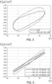
Figure 3 illustrates the results of the ferroelectric analysis conducted on a thin film made of PVDF and on a thin film formed with an undoped PVDF and BZT-BCT composite; -
Figure 4 illustrates the results of the ferroelectric analysis conducted on a thin film formed with a PVDF and 2%BCNZT composite present in quantities of 15%, 20% and 25% on the total weight of the composite; -
Figure 5 illustrates the plot of the capacitance C as a function of the frequency f in a composite material layer formed according to the present disclosure; -
Figure 6 illustrates the plot of the inductance Lp as a function of the frequency f in a composite material layer formed according to the present disclosure, for different percentages of dispersed phase load; -
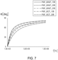
Figure 7 illustrates the plot of the phase Φ as a function of the frequency f in a composite material layer formed according to the present disclosure, for different percentages of dispersed phase load; -
Figure 8 illustrates the displacement s as a function of the frequency f in a composite material layer formed according to the present disclosure; -
Figure 9 illustrates the plot of the amplitude A as a function of the frequency f in a composite material layer formed according to the present disclosure and used respectively in an ultrasonic detector (A_DUT) and in an ultrasonic microphone (A_MIC); and -
Figure 10 shows an example ofdevice 20 using the present composite material. - The present description relates to a composite material comprising a fluoropolymer matrix and a filler formed by nanoparticles of a ceramic of the BZT-αBXT type wherein X is selected from Ca, Sn and Mn and α is a molar fraction selected in the range between 0.10-0.90 doped with at least one doping element selected from the group consisting of Nb, La, Mn, Nd and W, provided that when X is Mn, the doping element is not Mn. The nanoparticles have an average diameter comprised between 100 and 200 nm.
- Advantageously, the present composite material has shown improved ferroelectric and piezoelectric properties and inductive behavior.
- In particular, the presence of nanoparticles favors an exchange at the matrix-nanoparticle interface. Unlike the use of fibers, which favor the stiffening of the thin film, nanoparticles allow the conductive paths essential for the inductive properties and a flexible thin film to be obtained.
- In particular, the size range 100-200 nm maximizes the interface between polymer and filler. Average nanoparticle diameters greater than 200 nm do not guarantee an effective interface between the polymer and the ceramic for charge transfer. Instead, nanoparticles with an average diameter of less than 100 nm tend to coalescence, impeding a homogeneous distribution in the material.
- The doping elements La, Mn and Nd can replace the element in position A (barium and calcium site) while Nb and W can replace the element in position B (titanium and zirconium site).
- In one embodiment, the fluoropolymer is selected from the group consisting of polyvinylidene fluoride (PVDF) and its copolymers, in particular, copolymers of PVDF with hexafluoropropylene (HFP) or with trifluoroethylene (TrFE).
- In particular, PVDF and its copolymers may have a beta-phase percentage mass fraction, with respect to the sum of the masses of the crystalline phases, of at least 70%, more particularly between 86% and 99%.
- The ceramic of the BZT-αBXT type may be a ceramic of the Barium Zirconate Titanate-Barium Calcium Titanate (BZT-BCT) type, in particular a ceramic of the 1-α)Ba(Zr(0.2-0.5y)Ti(0.8-0.5y))NbyO3-αBa0.7Ca0.3(Ti(1-y)Nby)O3 type, where α indicates the ratio between BZT and BCT and y=0.01-5% by weight on the total weight of the ceramic indicates the degree of substitution of Nb with respect to the sum of Ti and Zr, in particular y=2% by weight on the total weight of the ceramic.
- The composite material has a ceramic (filler) content comprised between 10% and 25% by weight on the total weight of the composite, in particular 20%.
- Outside this range the properties begin to decay to a complete loss of inductive behavior. Filler percentages greater than 25% lead to an onset of coalescence phenomena, the frequency of which increases as the filler percentage increases; such coalescence phenomena lead to an increased possibility of electrical short circuits. In contrast, a filler percentage of less than 10% results in an uneven distribution of filler within the matrix.
- Hereinbelow there is described an embodiment of a process for producing a thin film formed with the composite material described above. In detail, the process comprises:
- a) submitting a dispersion of ceramic nanoparticles in an organic fluoropolymer solution to a first spin-coating step at a speed comprised between 500 and 1500 rpm, to a second spin-coating step at a speed comprised between 3500 and 5500 rpm; and to a third spin-coating step at a speed comprised between 8500 and 12000 rpm;
- b) submitting the product of step a) to a first annealing step at a temperature comprised between 60 and 70°C and to a second annealing step at a temperature comprised between 80 and 90°C.
- Advantageously, this method allows a homogeneous and uniform thin film to be formed.
- In particular, the first spin-coating step, conducted for example at 1000 rpm, leads to the application of the composite material on the entire surface of the substrate; the second spin-coating step, conducted for example at 4000 rpm, favors a first evaporation of the solvent and the third spin-coating step, conducted for example at 9000 rpm, favors the formation of the beta phase as it allows the complete stretching of the PVDF chains and the rotation of the groups H and F.
- Furthermore, the first annealing step favors a slow evaporation of the solvent which makes the surface of the thin film uniform and homogeneous; the second annealing step allows the polymer chains to consolidate after the total evaporation of the solvent.
- Thanks to its ferroelectric and piezoelectric properties, the composite material may be used for manufacturing electronic components such as acoustic sensors, in particular microphones, energy harvesting transducers and micro-actuators.
- Further characteristics will emerge from the following description of some merely illustrative and non-limiting examples.
- 17.78 g of PVDF powder are dissolved in a solution of 70 ml of DMSO and 30 ml of Acetone. The solution is placed on a magnetic plate and stirred by magnetic stirring at a temperature of 100°C.
- The BCNZT ceramic is prepared by Sol-Gel technique as described in
EP 4074672 . The precursor solution is then dried at 150°C and the powders are recovered. - Once recovered, the powders are homogenized and dry ground using a planetary ball mill at a speed of 400 rpm for 4 hours. They are subsequently calcined at 1400°C and wet regrinded for 8 hours with ethanol (1 ml) to obtain nanoparticles of the order of 100-200nm.
- The 2%BCNZT nanoparticles are added in different amounts (15%, 20% 25% by weight on the composite weight) to the PVDF solution and are dispersed by ultrasonication and stirring. The solution is left on a plate for approximately 10 days to reach stability.
- Once stabilized, the solution is deposited by spin-coating on a substrate to form a thin film. Three spin-coating steps are performed:
The method used envisages three steps: - 1000 rpm per 10 s;
- 4000 rpm per 30 s;
- 9000 rpm per 60 s.
- Subsequently the sample is placed for 10 min on a plate at 70°C for a first initial evaporation and subsequently on a plate at 90°C for another 10 min for the annealing step, finally it is cooled to room temperature T.
- The films have been submitted to X-ray diffraction studies to verify the formation of the PVDF phases.
-
Figure 1 shows the X-ray diffraction (XRD) spectrum of the composite sample comprising 25% of 2%BCNZT; from this it is clear that only the β-phase is present in the PVDF. The intensity of the 2%BCNZT peak also demonstrates a high homogeneity of the composite analyzed. - For the electrical characterization, a
sample 10 has been provided as shown inFigure 2 . - The
sample 10 comprises asemiconductor layer 11, for example of monocrystalline silicon; an insulatinglayer 12, for example of silicon oxide; alower electrode layer 13, formed by a TiO2/Pt multilayer; acomposite layer 14 of the present PVDF-BCNZT composite material; and a plurality ofupper electrodes 15 of Pt. - In the used sample, the stack of layers 11-13 has a total thickness of 700 um; the
composite layer 14 has a thickness of 2 um and theupper electrodes 15 have a thickness of 120 nm. - The sample is sprayed (Turbo-Pumped Thermal Evaporator K975X) with platinum to form the upper electrodes and etched at the end to contact the lower electrode. Alternatively, a sputtering process may also be used to form the upper electrodes.
- For all measurements, the electrodes were contacted with metal tips through manipulators on a hand-held spindle probe. Electrical property tests and impedance spectroscopy were performed with the Keysight B1500A semiconductor device analyzer. The ferroelectric properties were studied with the Aixact TFA TF2000E analyzer, applying a 30V, 5kHz triangular wave signal to the sample.
- In particular, the samples tested are films formed with:
- PVDF polymer only;
- Composite comprising PVDF and BCT-BZT;
- Composite comprising PVDF and 15% of 2%BCNZT;
- Composite comprising PVDF and 20% of 2%BCNZT;
- Composite comprising PVDF and 25% of 2%BCNZT.
- The results of the ferroelectric tests are shown in
Figures 3 and 4 . - PVDF and PVDF-BZTBCT thin films show broader ferroelectric properties associated with inductive behavior, likely due to conductive paths emerging in the PVDF matrix.
- The shape of the ferroelectric curves of
Figure 4 allows highlighting that the presence of Nb reduces the percolation path in the film which has a narrower characteristic with the same voltage. - Interesting properties of Nb-doped composites emerged thanks to impedance measurements. The samples were tested with the B1530 module of the B1500A, applying a 50mV AC signal and no DC polarization to the samples. With this module frequencies from 1kHz to 5MHz may be tested. These measurements confirmed the dielectric properties of the PVDF as shown in
Figure 5 . - The described composites also showed an inductive nature measuring impedance and phase, as shown in
Figures 6 and7 . - Finally, the piezoelectric properties were measured by a laser vibrometer (Polytec) on a cantilever-shaped device.
- Films with different doping percentages were submitted to vibrometric testing using the MSA-500 Micro System Analyzer (Polytec) to estimate the piezoelectric parameters. In particular, the device was submitted to an acoustic wave generated by a loudspeaker controlled by an external sinusoidal signal (periodic chirp of 3 V) and the displacement was measured using a laser vibrometer. This allowed the resonance frequency to be extracted.
Figure 8 shows the plot of the displacement as a function of the frequency presented by a device having a layer of the composite material containing PVDF and 20% of 2%BCNZT. - Once the resonance frequency was extracted, by setting voltage and frequency in proximity to the resonance, the deflection of the cantilever was estimated. The displacement and the corresponding value of the effective in-plane transverse piezoelectric coefficient e31f were shown in Table 1 according to the formula proposed by Mazzalai:

Figure 2 , the semiconductor layer 11-13), cf is the coverage factor of the electrodes, x2 is the length of the piezoelectric active area, x1 is the length of the laser impingement point, w(x2) is the deflection, V is the amplitude of the sinusoidal signal applied.Table 1 Content [%] Displacement Piezoelectric Coefficient PVDF BZTBCT Nb w(x2) [m] e31,f [C/m2] 15 15 0 2.00 e-9 0.672 15 20 0 3.30 e-9 1.109 15 15 2 4.25 e-9 1.785 15 20 2 9.00 e-9 3.781 15 25 2 2.70 e-9 1.134 - Furthermore, since a resonance frequency close to 4 kHz was detected, the behavior of various devices exposed to sound pressure was studied. The acoustic wave is sent from a speaker to the cantilever and with the Micro System Analyzer MSA-500 the response of a device comprising the described composite material of a certified commercial microphone was studied. The measurement was carried out by driving the speaker with a sinusoidal signal at various frequencies of the audible range, from 20Hz to 20 kHz. It has been found that the response of the device comprising the composite material comprising PVDF and 20% of 2%BCNZT follows the signal detected by the microphone, with an amplitude that differs by one tenth from the certified microphone, as shown in
Figure 9 , wherein A_Mic refers to the amplitude measured in the certified commercial microphone and A_DUT refers to the cantilever device using the present composite material. -
Figure 10 shows an example ofdevice 20 using the present composite material. - The
device 20 is for example a MEMS sensor or actuator; in particular a microphone. - The
device 20 has a suspendedstructure 21, here a cantilever, suspended over acavity 30. - The
cavity 30 is formed in asubstrate 31 and delimits the suspendedstructure 21 at the bottom. The suspendedstructure 21 may be monolithic with thesubstrate 31. The suspendedstructure 21 and the fixedstructure 31 are for example of monocrystalline silicon. - An insulating
layer 22, for example of silicon dioxide, extends above the suspendedstructure 21 and an actuation ordetection structure 32 extends on the insulatinglayer 22. - The actuation or
detection structure 32 comprises alower electrode layer 23, for example formed by a TiO2/Pt multilayer; acomposite layer 24, of the present PVDF_2% BCNZT composite material; and a plurality ofupper electrodes 25, for example of Pt. - Finally, it is clear that modifications and variations may be made to the composite material and the production process described and illustrated herein, without departing from the scope of the present invention, as defined in the attached claims.
Claims (11)
- A composite material comprising a fluoropolymer matrix and a filler consisting of nanoparticles of a ceramic of the BZT-αBXT type wherein X is selected from Ca, Sn and Mn and α is a molar fraction selected in the range between 0.10-0.90 doped with at least one doping element selected from the group consisting of Nb, La, Mn, Nd and W, provided that when X is Mn, the doping element is not Mn, wherein said nanoparticles have an average diameter comprised between 100 and 200 nm and wherein the filler is present in an amount comprised between 10 and 25% by weight on the total weight of the composite.
- The composite material according to claim 1, wherein the fluoropolymer matrix is selected from the group consisting of polyvinylidene fluoride (PVDF) and its copolymers.
- The composite material according to claim 2, wherein the copolymers are selected from the group consisting of copolymers of PVDF with hexafluoropropylene (HFP) or copolymers of PVDF with trifluoroethylene (TrFE).
- The composite material according to claim 2, wherein the polyvinylidene fluoride (PVDF) and its copolymers have a beta-phase percentage mass fraction, with respect to the sum of the masses of the crystalline phases, of at least 70%.
- The composite material according to claim 4, wherein the polyvinylidene fluoride (PVDF) and its copolymers have a beta-phase percentage mass fraction, with respect to the sum of the masses of the crystalline phases, comprised between 86% and 99%.
- The composite material according to claim 1, wherein the doping element is present in an amount comprised between 0.01% and 5% by weight on the total weight of the ceramic.
- The composite material according to claim 1, having a ceramic content of 20% by weight on the total weight of the composite.
- A process for producing a thin film comprising the composite material according to any of claims 1 to 7, comprising the steps of:a) submitting a dispersion of nanoparticles in an organic-phase fluoropolymer solution to a first spin-coating step at a speed comprised between 500 and 1500 rpm; to a second spin-coating step at a speed comprised between 3500 and 5500 rpm; and to a third spin-coating step at a speed comprised between 8500 and 12000 rpm;b) submitting the product of step a) to a first annealing step at a temperature comprised between 60 and 70°C and to a second annealing step at a temperature comprised between 80 and 90°C; wherein the nanoparticles are nanoparticles of a ceramic of the BZT-αBXT type wherein X is selected from Ca, Sn and Mn and α is a molar fraction selected in the range between 0.10-0.90 doped with at least one doping element selected from the group consisting of Nb, La, Mn, Nd and W, provided that when X is Mn, the doping element is not Mn, wherein said nanoparticles have an average diameter comprised between 100 and 200 nm and wherein the filler is present in an amount comprised between 10 and 25% by weight on the total weight of the composite.
- An electronic component comprising a piezoelectric layer including the composite material according to any of the preceding claims.
- The electronic component according to the preceding claim, forming an acoustic sensor.
- The electronic component according to the preceding claim, wherein the acoustic sensor is a microphone.
Applications Claiming Priority (1)
| Application Number | Priority Date | Filing Date | Title |
|---|---|---|---|
| IT102023000018027A IT202300018027A1 (en) | 2023-09-01 | 2023-09-01 | COMPOSITE MATERIAL WITH PIEZOELECTRIC PROPERTIES, MANUFACTURING PROCEDURE AND ELECTRONIC COMPONENT INCLUDING THE COMPOSITE MATERIAL |
Publications (1)
| Publication Number | Publication Date |
|---|---|
| EP4518636A1 true EP4518636A1 (en) | 2025-03-05 |
Family
ID=88689409
Family Applications (1)
| Application Number | Title | Priority Date | Filing Date |
|---|---|---|---|
| EP24197707.3A Pending EP4518636A1 (en) | 2023-09-01 | 2024-08-30 | Composite material with piezoelectric properties, production process thereof and electronic component comprising the composite material |
Country Status (4)
| Country | Link |
|---|---|
| US (1) | US20250081853A1 (en) |
| EP (1) | EP4518636A1 (en) |
| CN (1) | CN119552461A (en) |
| IT (1) | IT202300018027A1 (en) |
Citations (3)
| Publication number | Priority date | Publication date | Assignee | Title |
|---|---|---|---|---|
| US20110037015A1 (en) * | 2008-03-11 | 2011-02-17 | National Institute For Materials Science | Lead-free piezoelectric material |
| CN115028864A (en) * | 2022-06-10 | 2022-09-09 | 西北大学 | Element-doped BCZT/PVDF core-shell material, flexible film, preparation method and capacitor |
| EP4074672A1 (en) | 2021-04-15 | 2022-10-19 | STMicroelectronics S.r.l. | Method for the preparation of a lead-free piezoelectric material and precursor solution |
-
2023
- 2023-09-01 IT IT102023000018027A patent/IT202300018027A1/en unknown
-
2024
- 2024-08-29 US US18/819,799 patent/US20250081853A1/en active Pending
- 2024-08-30 CN CN202411208728.3A patent/CN119552461A/en active Pending
- 2024-08-30 EP EP24197707.3A patent/EP4518636A1/en active Pending
Patent Citations (3)
| Publication number | Priority date | Publication date | Assignee | Title |
|---|---|---|---|---|
| US20110037015A1 (en) * | 2008-03-11 | 2011-02-17 | National Institute For Materials Science | Lead-free piezoelectric material |
| EP4074672A1 (en) | 2021-04-15 | 2022-10-19 | STMicroelectronics S.r.l. | Method for the preparation of a lead-free piezoelectric material and precursor solution |
| CN115028864A (en) * | 2022-06-10 | 2022-09-09 | 西北大学 | Element-doped BCZT/PVDF core-shell material, flexible film, preparation method and capacitor |
Non-Patent Citations (5)
| Title |
|---|
| BARBATO P ET AL: "Green Synthesis of Piezoelectric Thin Films based on Niobium Doped Barium Zirconate Titanate - Barium Calcium Titanate (Nb-BZT-BCT)", vol. 101, 30 July 2023 (2023-07-30), IT, pages 73 - 78, XP093136020, ISSN: 2283-9216, Retrieved from the Internet <URL:https://www.cetjournal.it/cet/23/101/013.pdf> DOI: 10.3303/CET23101013 * |
| DASH S ET AL: "Enhancing functional properties of PVDF-HFP/BZT-BCT polymer-ceramic composites by surface hydroxylation of ceramic fillers", CERAMICS INTERNATIONAL, ELSEVIER, AMSTERDAM, NL, vol. 47, no. 23, 23 August 2021 (2021-08-23), pages 33563 - 33576, XP086830685, ISSN: 0272-8842, [retrieved on 20210823], DOI: 10.1016/J.CERAMINT.2021.08.265 * |
| SARKAR L ET AL: "Preparation and optimization of PVDF thin films for miniaturized sensor and actuator applications", SMART MATERIALS AND STRUCTURES, IOP PUBLISHING LTD., BRISTOL, GB, vol. 30, no. 7, 28 May 2021 (2021-05-28), pages 75013, XP020367162, ISSN: 0964-1726, [retrieved on 20210528], DOI: 10.1088/1361-665X/ABFF15 * |
| SHAIK H ET AL: "Towards [beta]-phase formation probability in spin coated PVDF thin films", JOURNAL OF POLYMER RESEARCH, SPRINGER NETHERLANDS, DORDRECHT, vol. 24, no. 3, 9 February 2017 (2017-02-09), pages 1 - 6, XP036205348, ISSN: 1022-9760, [retrieved on 20170209], DOI: 10.1007/S10965-017-1191-X * |
| XU C ET AL: "Enhanced piezoelectric properties and thermal stability in tetragonal-structured (Ba,Ca)( Zr,Ti)O3 piezoelectrics substituted with trace amount of Mn", CERAMICS INTERNATIONAL, ELSEVIER, AMSTERDAM, NL, vol. 42, no. 14, 19 July 2016 (2016-07-19), pages 16109 - 16115, XP029686958, ISSN: 0272-8842, DOI: 10.1016/J.CERAMINT.2016.07.125 * |
Also Published As
| Publication number | Publication date |
|---|---|
| IT202300018027A1 (en) | 2025-03-01 |
| US20250081853A1 (en) | 2025-03-06 |
| CN119552461A (en) | 2025-03-04 |
Similar Documents
| Publication | Publication Date | Title |
|---|---|---|
| US8310134B2 (en) | Composition for energy generator, storage, and strain sensor and methods of use thereof | |
| Khan et al. | Piezoelectric thin films: an integrated review of transducers and energy harvesting | |
| US20110192016A1 (en) | Energy conversion materials fabricated with boron nitride nanotubes (BNNTs) and BNNT polymer composites | |
| Han et al. | Origin of in situ domain formation of heavily Nb-doped Pb (Zr, Ti) O3 thin films sputtered on Ir/TiW/SiO2/Si substrates for mobile sensor applications | |
| Chamankar et al. | Comparing the piezo, pyro and dielectric properties of PZT particles synthesized by sol–gel and electrospinning methods | |
| US12281223B2 (en) | Piezoelectric composite material and method | |
| Bowen et al. | Manufacture and characterization of high activity piezoelectric fibres | |
| Dias et al. | Recent advances in ceramic-polymer composite electrets | |
| Rajala et al. | High bending-mode sensitivity of printed piezoelectric poly (vinylidenefluoride-co-trifluoroethylene) sensors | |
| Verma et al. | Interdependence of piezoelectric coefficient and film thickness in LiTaO3 cantilevers | |
| Wang et al. | Progress on the applications of piezoelectric materials in sensors | |
| Wang et al. | Piezoelectric thick films and their application in MEMS | |
| Komljenovic et al. | Piezo-to-piezo (P2P) conversion: simultaneous β-phase crystallization and poling of ultrathin, transparent and freestanding homopolymer PVDF films via MHz-order nanoelectromechanical vibration | |
| US20250081853A1 (en) | Composite material with piezoelectric properties, production process and electronic component comprising the composite material | |
| Kim et al. | Beam vibration control using cellulose-based electro-active paper sensor | |
| Su et al. | A curve-structured flexible pmut with enhanced acoustic sensitivity | |
| Lau et al. | Ferroelectric lead magnesium niobate–lead titanate single crystals for ultrasonic hydrophone applications | |
| Yang et al. | Manipulation of the oriented amorphous fraction of poly (vinylidene fluoride-co-trifluoroethylene) films by thermal annealing for high piezoelectricity | |
| Zhang et al. | Electromechanical coupling of lead zirconate titanate nanofibres | |
| Ryu et al. | Ferroelectric polymer PVDF-based nanogenerator | |
| Fuentes-Fernandez et al. | Fabrication of relaxer-based piezoelectric energy harvesters using a sacrificial poly-Si seeding layer | |
| Sierra et al. | Electrostriction contribution to the electromechanical response of cast chitosan films | |
| Riaz et al. | Piezoelectric Acoustic Vibration Sensor Based on Flexible-PCB Spin-coated with PVDF-TrFE | |
| Kunwar et al. | Investigating the Effects of Solvents and Nanocomposites on Tailoring the Elastic Modulus of Piezoelectric Thin Film PVDF-TrFE | |
| Isarakorn et al. | Energy harvesting MEMS device based on an epitaxial PZT thin film: fabrication and characterization |
Legal Events
| Date | Code | Title | Description |
|---|---|---|---|
| PUAI | Public reference made under article 153(3) epc to a published international application that has entered the european phase |
Free format text: ORIGINAL CODE: 0009012 |
|
| STAA | Information on the status of an ep patent application or granted ep patent |
Free format text: STATUS: THE APPLICATION HAS BEEN PUBLISHED |
|
| AK | Designated contracting states |
Kind code of ref document: A1 Designated state(s): AL AT BE BG CH CY CZ DE DK EE ES FI FR GB GR HR HU IE IS IT LI LT LU LV MC ME MK MT NL NO PL PT RO RS SE SI SK SM TR |
|
| STAA | Information on the status of an ep patent application or granted ep patent |
Free format text: STATUS: REQUEST FOR EXAMINATION WAS MADE |
|
| 17P | Request for examination filed |
Effective date: 20250812 |
|
| RIC1 | Information provided on ipc code assigned before grant |
Ipc: H10N 30/077 20230101AFI20251114BHEP Ipc: H04R 17/02 20060101ALI20251114BHEP Ipc: H10N 30/092 20230101ALI20251114BHEP Ipc: H10N 30/85 20230101ALI20251114BHEP Ipc: H10N 30/30 20230101ALN20251114BHEP Ipc: H10N 30/853 20230101ALN20251114BHEP |
|
| GRAP | Despatch of communication of intention to grant a patent |
Free format text: ORIGINAL CODE: EPIDOSNIGR1 |
|
| STAA | Information on the status of an ep patent application or granted ep patent |
Free format text: STATUS: GRANT OF PATENT IS INTENDED |
|
| INTG | Intention to grant announced |
Effective date: 20260105 |
|
| GRAS | Grant fee paid |
Free format text: ORIGINAL CODE: EPIDOSNIGR3 |
|
| GRAA | (expected) grant |
Free format text: ORIGINAL CODE: 0009210 |
|
| STAA | Information on the status of an ep patent application or granted ep patent |
Free format text: STATUS: THE PATENT HAS BEEN GRANTED |