EP4518120A1 - Control device and method for switching voltage regulator - Google Patents
Control device and method for switching voltage regulator Download PDFInfo
- Publication number
- EP4518120A1 EP4518120A1 EP24193712.7A EP24193712A EP4518120A1 EP 4518120 A1 EP4518120 A1 EP 4518120A1 EP 24193712 A EP24193712 A EP 24193712A EP 4518120 A1 EP4518120 A1 EP 4518120A1
- Authority
- EP
- European Patent Office
- Prior art keywords
- signal
- measurement
- offset
- control
- voltage
- Prior art date
- Legal status (The legal status is an assumption and is not a legal conclusion. Google has not performed a legal analysis and makes no representation as to the accuracy of the status listed.)
- Pending
Links
Images




Classifications
-
- H—ELECTRICITY
- H02—GENERATION; CONVERSION OR DISTRIBUTION OF ELECTRIC POWER
- H02M—APPARATUS FOR CONVERSION BETWEEN AC AND AC, BETWEEN AC AND DC, OR BETWEEN DC AND DC, AND FOR USE WITH MAINS OR SIMILAR POWER SUPPLY SYSTEMS; CONVERSION OF DC OR AC INPUT POWER INTO SURGE OUTPUT POWER; CONTROL OR REGULATION THEREOF
- H02M3/00—Conversion of DC power input into DC power output
- H02M3/02—Conversion of DC power input into DC power output without intermediate conversion into AC
- H02M3/04—Conversion of DC power input into DC power output without intermediate conversion into AC by static converters
- H02M3/10—Conversion of DC power input into DC power output without intermediate conversion into AC by static converters using discharge tubes with control electrode or semiconductor devices with control electrode
- H02M3/145—Conversion of DC power input into DC power output without intermediate conversion into AC by static converters using discharge tubes with control electrode or semiconductor devices with control electrode using devices of a triode or transistor type requiring continuous application of a control signal
- H02M3/155—Conversion of DC power input into DC power output without intermediate conversion into AC by static converters using discharge tubes with control electrode or semiconductor devices with control electrode using devices of a triode or transistor type requiring continuous application of a control signal using semiconductor devices only
- H02M3/156—Conversion of DC power input into DC power output without intermediate conversion into AC by static converters using discharge tubes with control electrode or semiconductor devices with control electrode using devices of a triode or transistor type requiring continuous application of a control signal using semiconductor devices only with automatic control of output voltage or current, e.g. switching regulators
- H02M3/158—Conversion of DC power input into DC power output without intermediate conversion into AC by static converters using discharge tubes with control electrode or semiconductor devices with control electrode using devices of a triode or transistor type requiring continuous application of a control signal using semiconductor devices only with automatic control of output voltage or current, e.g. switching regulators including plural semiconductor devices as final control devices for a single load
- H02M3/1582—Buck-boost converters
-
- H—ELECTRICITY
- H02—GENERATION; CONVERSION OR DISTRIBUTION OF ELECTRIC POWER
- H02M—APPARATUS FOR CONVERSION BETWEEN AC AND AC, BETWEEN AC AND DC, OR BETWEEN DC AND DC, AND FOR USE WITH MAINS OR SIMILAR POWER SUPPLY SYSTEMS; CONVERSION OF DC OR AC INPUT POWER INTO SURGE OUTPUT POWER; CONTROL OR REGULATION THEREOF
- H02M1/00—Details of apparatus for conversion
- H02M1/0003—Details of control, feedback or regulation circuits
- H02M1/0009—Devices or circuits for detecting current in a converter
-
- H—ELECTRICITY
- H02—GENERATION; CONVERSION OR DISTRIBUTION OF ELECTRIC POWER
- H02M—APPARATUS FOR CONVERSION BETWEEN AC AND AC, BETWEEN AC AND DC, OR BETWEEN DC AND DC, AND FOR USE WITH MAINS OR SIMILAR POWER SUPPLY SYSTEMS; CONVERSION OF DC OR AC INPUT POWER INTO SURGE OUTPUT POWER; CONTROL OR REGULATION THEREOF
- H02M1/00—Details of apparatus for conversion
- H02M1/0003—Details of control, feedback or regulation circuits
- H02M1/0025—Arrangements for modifying reference values, feedback values or error values in the control loop of a converter
-
- H—ELECTRICITY
- H02—GENERATION; CONVERSION OR DISTRIBUTION OF ELECTRIC POWER
- H02M—APPARATUS FOR CONVERSION BETWEEN AC AND AC, BETWEEN AC AND DC, OR BETWEEN DC AND DC, AND FOR USE WITH MAINS OR SIMILAR POWER SUPPLY SYSTEMS; CONVERSION OF DC OR AC INPUT POWER INTO SURGE OUTPUT POWER; CONTROL OR REGULATION THEREOF
- H02M1/00—Details of apparatus for conversion
- H02M1/14—Arrangements for reducing ripples from DC input or output
-
- H—ELECTRICITY
- H02—GENERATION; CONVERSION OR DISTRIBUTION OF ELECTRIC POWER
- H02M—APPARATUS FOR CONVERSION BETWEEN AC AND AC, BETWEEN AC AND DC, OR BETWEEN DC AND DC, AND FOR USE WITH MAINS OR SIMILAR POWER SUPPLY SYSTEMS; CONVERSION OF DC OR AC INPUT POWER INTO SURGE OUTPUT POWER; CONTROL OR REGULATION THEREOF
- H02M3/00—Conversion of DC power input into DC power output
- H02M3/02—Conversion of DC power input into DC power output without intermediate conversion into AC
- H02M3/04—Conversion of DC power input into DC power output without intermediate conversion into AC by static converters
- H02M3/10—Conversion of DC power input into DC power output without intermediate conversion into AC by static converters using discharge tubes with control electrode or semiconductor devices with control electrode
- H02M3/145—Conversion of DC power input into DC power output without intermediate conversion into AC by static converters using discharge tubes with control electrode or semiconductor devices with control electrode using devices of a triode or transistor type requiring continuous application of a control signal
- H02M3/155—Conversion of DC power input into DC power output without intermediate conversion into AC by static converters using discharge tubes with control electrode or semiconductor devices with control electrode using devices of a triode or transistor type requiring continuous application of a control signal using semiconductor devices only
- H02M3/156—Conversion of DC power input into DC power output without intermediate conversion into AC by static converters using discharge tubes with control electrode or semiconductor devices with control electrode using devices of a triode or transistor type requiring continuous application of a control signal using semiconductor devices only with automatic control of output voltage or current, e.g. switching regulators
- H02M3/157—Conversion of DC power input into DC power output without intermediate conversion into AC by static converters using discharge tubes with control electrode or semiconductor devices with control electrode using devices of a triode or transistor type requiring continuous application of a control signal using semiconductor devices only with automatic control of output voltage or current, e.g. switching regulators with digital control
-
- H—ELECTRICITY
- H02—GENERATION; CONVERSION OR DISTRIBUTION OF ELECTRIC POWER
- H02M—APPARATUS FOR CONVERSION BETWEEN AC AND AC, BETWEEN AC AND DC, OR BETWEEN DC AND DC, AND FOR USE WITH MAINS OR SIMILAR POWER SUPPLY SYSTEMS; CONVERSION OF DC OR AC INPUT POWER INTO SURGE OUTPUT POWER; CONTROL OR REGULATION THEREOF
- H02M3/00—Conversion of DC power input into DC power output
- H02M3/02—Conversion of DC power input into DC power output without intermediate conversion into AC
- H02M3/04—Conversion of DC power input into DC power output without intermediate conversion into AC by static converters
- H02M3/10—Conversion of DC power input into DC power output without intermediate conversion into AC by static converters using discharge tubes with control electrode or semiconductor devices with control electrode
- H02M3/145—Conversion of DC power input into DC power output without intermediate conversion into AC by static converters using discharge tubes with control electrode or semiconductor devices with control electrode using devices of a triode or transistor type requiring continuous application of a control signal
- H02M3/155—Conversion of DC power input into DC power output without intermediate conversion into AC by static converters using discharge tubes with control electrode or semiconductor devices with control electrode using devices of a triode or transistor type requiring continuous application of a control signal using semiconductor devices only
- H02M3/156—Conversion of DC power input into DC power output without intermediate conversion into AC by static converters using discharge tubes with control electrode or semiconductor devices with control electrode using devices of a triode or transistor type requiring continuous application of a control signal using semiconductor devices only with automatic control of output voltage or current, e.g. switching regulators
- H02M3/158—Conversion of DC power input into DC power output without intermediate conversion into AC by static converters using discharge tubes with control electrode or semiconductor devices with control electrode using devices of a triode or transistor type requiring continuous application of a control signal using semiconductor devices only with automatic control of output voltage or current, e.g. switching regulators including plural semiconductor devices as final control devices for a single load
Definitions
- the present invention relates to a control device and a method for switching voltage regulator.
- switching voltage regulators are devices having the function of converting an input direct voltage (DC) into an output direct voltage. They may have different topologies, one of the most widespread being the four-switch non-inverting topology.
- Switching voltage regulators may also operate according to different modes, including the buck control mode (step-down) and the boost control mode (step-up).
- Regulators so-called buck-boost regulators
- buck-boost regulators are also known which use both control modes in different operating steps of the regulator, depending on the value of the input voltage and, in particular, on the relationship (greater or smaller) of the input voltage with respect to the output voltage.
- Switching voltage regulators of this type are based on the regulation of the duty-cycle, i.e. the on and off times of switches and may be represented by the block diagram of Figure 1 .
- Figure 1 shows a voltage regulator 1 comprising a switching circuit 2 and a control device 3.
- the switching circuit 2 is here formed by a first half-bridge 4 and a second half-bridge 5.
- the first half-bridge 4 is formed by a first high-side switch (first HSS 11) and a first low-side switch (first LSS 12), series-coupled between an input terminal 6 and a reference potential line (ground) 7. An input voltage Vi is applied between the input terminal 6 and the reference potential line 7.
- the second half-bridge 5 is formed by a second high-side switch (second HSS 13) and a second low-side switch (second LSS 14), series-coupled between an output terminal 9 and the reference potential line 7.
- An output voltage Vo referred to ground, is present at the output terminal 9 and is provided to a load 18.
- the switches 11-14 are typically formed by MOSFET devices.
- the low-side switches (first LSS 12 and second LSS 14) have source terminals mutually coupled at a common node 17.
- a sense resistor 19 is arranged between the common node 17 and the reference potential line 7.
- An inductor 20 is coupled between intermediate nodes 15, 16 of the first and the second half-bridges 4, 5.
- the control device 3 is coupled to the input terminal 6 and the output terminal 9 and receives a reference voltage V ref . Furthermore, the control device 3 is coupled to the control terminals of the switches 11-14, as well as to the sense resistor 19, so as to operate a current control of the switching circuit 2.
- Regulators operating in buck-boost control mode operate in buck control mode when the input voltage Vi is greater than the output voltage Vo and vice versa.
- transition phases called buck-boost transition phases, may be envisaged.
- control device 3 generates a first switching signal TON1 and a second switching signal TOFF1, which are digital and opposite to each other.
- Signals TON1 and TOFF1 are provided respectively to the first HSS 11 and to the first LSS 12, which therefore switch in opposite manners.
- the second HSS 13 is always on (in Figure 2A it receives a high logic signal "1") and the second LSS 14 is always off (in Figure 2A it receives a low logic signal "0") .
- the switching circuit 2 when the first switching signal TON1 is high (logic signal “1") and the second switching signal TOFF1 is low (logic signal “0"), the first HSS 11 is on, the first LSS 12 is off, and a current (inductor current I L ) flows into the first HSS 11, the inductor 20, and the second HSS 13, as shown by a dashed line. Since the voltage on the inductor 20 is positive and equal to (Vi-Vo), the inductor current I L increases linearly with slope (Vi-Vo)/L (L being the inductance of the inductor 20) .
- the first HSS 11 switches off, the first LSS 12 switches on, and the inductor current I L flows into the first LSS 12, the inductor 20 and the second HSS 13, as shown by a dash-dotted line.
- the inductor current I L decreases linearly with slope -Vo/L.
- the sense resistor 19 senses the inductor current I L , provided to the control device 3.
- control device 3 controls on and off, in an alternated way, of the second HSS 13 and the second LSS 14; furthermore, it keeps the first HSS 11 always on and the first LSS 12 always off, as shown in Figure 2B .
- control device 3 generates a third switching signal TOFF2 and a fourth switching signal TON2, which are digital and opposite to each other.
- Signals TOFF2 and TON2 are provided respectively to the second HSS 13 and to the second LSS 14, which therefore switch in opposite manners.
- the first HSS 11 is always on (in Figure 2B it receives a high logic signal "1") and the first LSS 12 is always off (it receives a low logic signal "0").
- the switching circuit 2 when the fourth switching signal TON2 is high (logic signal “1") and the third switching signal TOFF2 is low (logic signal "0"), the second HSS 13 is off, the second LSS 14 is on, and the inductor current I L flows into the first HSS 11, the inductor 20, and the second LSS 14, as shown by a dash-dotted line. Therefore, the voltage on the inductor 20 is positive (equal, in a first approximation, to Vi, neglecting the drop on the sense resistor 19) and the inductor current I L increases linearly with slope Vi/L.
- the sense resistor 19 senses the inductor current I L and provides it to the control device 3.
- the second LSS 14 switches off, the second HSS 13 switches on, and the inductor current I L flows into the first HSS 11, the inductor 20 and the second HSS 13, as shown by a dashed line.
- the inductor current I L decreases linearly with slope (Vi-Vo) /L.
- buck-boost mixed control mode
- boost-mode control cycles and boost-mode control cycles are alternated, controlling selective switching-on and switching-off of all the switches 11-14 of the half-bridges 4, 5.
- the control device 3 uses the inductor current I L sensed by the sense resistor 19 (the valley value, in buck control mode, and the peak value, in boost control mode) to control the output voltage Vo and keep it proximate to the reference value V ref .
- control device 3 generally performs a current loop control of the switching circuit 2.
- An example of control device 3 operating in this manner is shown in the simplified block diagram of Figure 3 .
- the modulation signal PWM has a fixed period and the PWM modulator 34 modifies, in use, the duty-cycle of each period of the modulation signal PWM in response to the comparison between the reference current I C +I s and the inductor current I L .
- Figure 4 shows with a circle the acquisition points of the value of the inductor current I L , at the valleys, when the voltage regulator 1 operates in buck mode, and at the peaks, when the voltage regulator 1 operates in boost mode, as indicated above.
- Figure 4 also shows the desired average output current Io and the plot of the control signal Ic of Figure 3 (indicative of the transition threshold) to obtain the desired average output current Io.
- the valley value of the inductor current I L is approximately equal to the value of the control signal Ic (indicated by Ic(buck)).
- the comparison between the inductor current I L and the control current Ic occurs at the peaks of the inductor current I L (as indicated in the circles).
- control current Ic has a higher value (indicated in Figure 4 by I C (boost)), correlated to the peak value of the inductor current I L ; thereby, the average output current is equal to the desired value Io.
- Figure 4 also shows the corresponding plot of the output voltage Vo; as is noted, in the passage from the buck control mode to the boost control mode, the output voltage Vo undergoes a significant excursion (reduction) ⁇ Vo. This reduction, whose value also depends on the control loop bandwidth, is however undesired in a voltage regulator.
- the aim of the present invention is to provide a solution overcoming the drawbacks of the prior art.
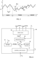
- Figure 5 shows approximately the behavior of the control current Ic during a transient from a buck control mode (with valley current measurement) to a boost control mode (with peak current measurement) and highlights the output current difference ⁇ Io between the (desired) regulated average current Io and the average value Im of the inductor current I L , shown with horizontal dashed line, during transition, for the switching circuit 2 of Figure 3 .
- the output current difference ⁇ Io is very high immediately after switching to the peak measurement mode and gradually reduces to reach the (desired) regulated average current Io in boost control mode.
- a buck-boost control mode is used.
- this output current difference ⁇ Io corresponds to the current necessary to keep the output voltage Vo at a regulation value and that, by compensating this output current difference ⁇ Io, both the excursion ⁇ Vo in the voltage output and the duration of the transient when switching between the valley and peak measurement modes may be significantly reduced.
- Figure 6 shows a control device 50 capable of compensating the output current difference ⁇ Io discussed above.
- the control device 50 is couplable to a switching circuit, similarly to the control device 3 in Figure 1 .
- the switching circuit is therefore not shown in Figure 5 and may be formed like the switching circuit 2 of Figure 1 .
- the control device 50 has a general structure similar to the control device 3 of Figure 3 . Consequently, the elements of the control device 50 common to the control device 3 of Figure 3 have been provided with the same reference numbers and will only be described briefly.
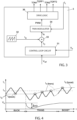
- control device 50 comprises a control loop circuit 31, which generates the control signal I C , a current signal, correlated to the difference between the output voltage Vo and a reference voltage V ref ; a ramp generator 32, which generates a current ramp I s ; an adder node 33 which receives the current ramp I s and the control signal I C and generates a reference current I R ; a PWM modulator 34, which compares the inductor current I L with the reference current I R and generates a pulse width modulation signal PWM; and a drive logic 36, which generates switch control signals TON1, TOFF1, TON2, TOFF2 from the modulation signal PWM, similarly to the control device 3 of Figure 3 .
- the control device 50 further comprises an offset generator 51 generating an offset current I OFFSET which is added to the control signal I C and the current ramp I s in the adder node 33 at the transient between the buck and boost control modes, in particles in the transient from the buck control mode to the boost control mode.
- the offset current I OFFSET may be maintained only during the transient phase or throughout the peak control phase.
- the offset generator 51 receives an activation signal M, for example a digital signal whose logic level determines the active or inactive state of the offset generator 51.
- the activation signal M is also indicative of the measurement mode of the current, valley or peak current, and therefore has a first logic state (for example a high logic state) during the valley measurement operation and a second logic level, in the example a low logic state, in the valley measurement mode.
- the activation signal M may be generated in different manners: for example, as shown in Figure 7 , the activation signal M is generated by a mode sense block 52 receiving at input the output voltage Vo and the input voltage Vi.
- the mode sense block 52 may be a simple comparator that compares the input voltage Vi and the output voltage Vo to each other and generates the activation signal M as a digital signal having a first logic value (for example a high value) when Vi > Vo and conversely a second logic value (a low value in the example).
- a hysteresis may be used in the comparison between Vi and Vo (for example using a hysteresis threshold comparator) to prevent the voltage regulator from oscillating between the high value and the low value when Vi is exactly equal to Vo.
- the activation signal M may also be sent to the PWM modulator for the decision on sampling the inductor current I L at the valleys (buck control mode) or the peaks (boost control mode) and/or to the drive logic 36 for the decision of the drive sequence of the switches 11-14.
- the activation signal M is also used in buck-boost control phase, if provided, wherein the valley current for Vi > Vo and the peak current for Vi ⁇ Vo are sensed.
- the mode sense block 52 senses a predetermined ratio between the input voltage Vi and the output voltage Vo, it switches the activation signal M, the offset generator 51 is activated and provides the adder node 33 with the offset current I OFFSET , which adds to the control signal I C and the current ramp Is.
- the value of the offset current I OFFSET may be a fixed value, set in the factory or during the setting phase of the control device 50; or it may be a configurable or variable value.
- the value of the offset current I OFFSET may be calculated by an analog or digital circuit internal or external to the offset generator 51 on the basis of the electrical quantities (Vi, Vo, I L , ...) of the voltage regulator.
- this value may be set on the basis of simulations.
- the input voltage Vi becomes lower than the output voltage Vo and the activation signal M switches from high to low.
- Figure 8 shows that, while the curve of the reference current I RB obtainable with the control device 3 of Figure 2 has a significant reduction (as discussed above with reference to Figure 4 ), the curve of the reference current I RA obtainable with the control device 50 of Figure 7 has an increase (current step), due to the injection of the offset current I OFFSET . Furthermore, while the inductor current I LB obtainable with the control device 3 of Figure 2 has a significant reduction and is detectable for several operating cycles, the inductor current I LA obtainable with the control device 50 of Figure 7 has a minimum reduction in the maximum and minimum values.
- the output voltage Vo shows a lower reduction with respect to the boost steady value, as shown in Figure 9 , wherein the output voltage Vo is indicated by VoA and the output voltage Vo obtainable with the control device 3 of Figure 2 is indicated by VoB.
- the output voltage VoA obtainable with the control device 50 of Figure 7 has a reduction (with respect to the regulated boost value) of about 50% lower than the excursion presented by the voltage output VoB.
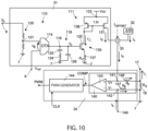
- Figure 10 shows a possible implementation of the control loop circuit 31 and the PWM modulator 34.
- These circuits described in detail in Italian patent application 102022000013240, filed on 6/22/2022 , corresponding to the European patent application 23178174.1, filed on 6/8/2023 , US patent application 18330754, filed on 6/7/2023 , and Chinese patent application 202310742484.6, filed on 6/23/2023 , are briefly described hereinbelow, for completeness.
- the control loop circuit 31 comprises a compensation module 110, receiving the output voltage Vo and the reference voltage V ref and providing a control voltage V c , and a voltage-to-current conversion module 111, providing the control signal I C as a function of the control voltage V c .
- the compensation module 110 comprises an error amplifier, here an operational transconductance amplifier (OTA) 114 having an output 116 providing an error signal V E , indicative of the difference between the output voltage V o and the reference voltage V ref , and a compensation network 118 coupled to the output 116 and generating the control voltage V c .
- OTA operational transconductance amplifier
- the compensation module 110 further comprises a voltage divider 120 coupled between the output terminal 9 and the reference potential line 7 and having an intermediate node 121.
- the OTA 114 has a first input coupled to the reference node 8 and a second input coupled to the intermediate node 121 of the voltage divider 120.
- the OTA 114 compares the reference voltage V ref with a fraction of the output voltage V o .
- the compensation network 118 is a parallel circuit coupled between the output terminal 6 and the reference potential line 7 and comprises a compensation resistor 124 and compensation capacitors 125, 126.
- the voltage-to-current conversion module 111 is formed by a first mirror branch 130 and a second mirror branch.
- the second mirror branch comprises an output transistor 131 of the PMOS type.
- the first mirror branch 130 is a series circuit coupled between the reference potential line 7 and a supply line 133 at a supply voltage V CC with respect to the reference potential line 7, and comprising a first transistor 135, here of the NMOS type, a second transistor 136, here of the PMOS type, and a control resistor 137 having resistance R C .
- the first transistor 135 has a gate terminal coupled to the output 116 of the OTA 114, and therefore receives the control voltage V C .
- the second transistor 136 has the source terminal connected to the supply node 133 and the gate terminal connected to the drain terminal.
- the gate terminal of the second transistor 136 is connected to the gate terminal of the output transistor 131.
- the first mirror branch 130 generates an intermediate control current I' c , as a function of the control voltage V c .
- the first and the second mirror branches 130, 131 have a current mirror ratio of 1:N, so that the control loop circuit 31 provides at output the control signal I C equal to N ⁇ I'c.
- the PWM modulator 34 comprises a current comparator 140, providing a comparison signal COMP, and a PWM generator 144, which generates the modulation signal PWM from a clock signal CLK and the comparison signal COMP.
- the current comparator 140 comprises a comparator element 143 having a positive input 141 and a negative input 142 and providing at output the comparison signal COMP.
- the current comparator 140 further comprises a first resistor 146 having resistance R A , coupled between the positive input 141 of the comparator element 143 and a first terminal of the sense resistor 19 (connected to the common node 17 of the switching circuit 2 of Figure 1 ); and a second resistor 147 having resistance R B , coupled between the negative input 142 of the comparator element 143 and a second terminal of the sense resistor 19 (connected to the reference potential line 7).
- the positive input 141 of the comparator element 143 is coupled to an output of the adder node 33 and the negative input 142 of the comparator element 143 is coupled to a bias node 149 providing a bias current I b .
- the configuration shown of the current comparator 140 refers to the valley control mode.
- a pair of switches (not shown) connects the output of the adder node 33 to both inputs 141 and 142 of the comparator element 143 and another pair of switches (not shown) connects the bias node 149 to both inputs 141 and 142.
- These switches are controlled so that, in peak control mode, the output of the adder node 33 is coupled to the negative input 142 of the comparator element 143 and the bias node 149 is coupled to the positive input 141 of the comparator element 143.
- the PWM generator 144 provides the modulation signal PWM, which is digital, whose period is a function of the period T of the clock signal CLK, and whose duty-cycle is variable in each cycle (or period) of the modulation signal PWM, in a per se known manner.
- the mirror circuit 131, 136 may be missing; in this case the drain terminal of the first transistor 135 may be connected directly to the adder node 33; with this solution, the current flowing into the first transistor 135 already represents the control signal I C provided to the adder node 33 (although of different sign).
- valley or peak current measurement mode is selected in the design step based on the ratio between the input voltage Vi and the output voltage Vo and other functions (for example, current limitation).
- the duration of the switch-on time of the high-side transistor might be too short to allow correct operation of the current comparator (140 in Figure 10 ).
- using a measurement mode based on the valleys of the inductor current may be useful, because in this manner the current comparator has more time to sense the inductor current during the switch-off phase of the high-side transistor.
- Switching from peak current sense mode to valley current sense mode also introduces an error in the current limitation value. This error may also be resolved by injecting an offset current.
- Figure 11 shows an embodiment of a voltage converter operating only in buck mode, with switches arranged externally to the switching circuit and with measurement of inductor current both at the peaks and at the valleys, alternately to each other, according to the operating conditions.
- Figure 11 shows a voltage converter 70 comprising a switching circuit 71 and a control device 73.
- the switching circuit 71 is here formed by a half-bridge circuit 74 comprising a high-side switch (HSS 75) and a low-side switch (LSS 76), receiving respective control signals T_HS and T_LS (similar for example to the first switching signal TON1 and, respectively, to the second switching signal TOFF1 of Figures 1 , 6 and 7 ) and series-connected between an input terminal 77 and a reference potential line (ground) 78.
- An input voltage Vi is applied between the input terminal 77 and the reference potential line 78 and an input capacitor 79, on which the input voltage Vi is applied, is coupled to the input terminal 77.
- An inductor 80 has a first terminal coupled to an intermediate node 81 of the half-bridge 74.
- a sense resistor 82 is coupled between a second terminal of the inductor 80 and an output terminal 83.
- An output capacitor 84 receiving the output voltage Vo, is coupled to the output terminal 83.
- the control device 72 has a structure similar to the control device 50 of Figure 7 ; the elements of the control device 72 common to the control device 50 have therefore been provided with the same reference numbers and will not be described.
- the mode sense block 52 is replaced by an activation block 87 based on sensing the ratio between the output voltage Vo and the input voltage Vi.
- the activation block 87 verifies whether the ratio between the output voltage Vo and the input voltage Vi is greater than a threshold value D TH , for example a fixed value such as 0.5.
- the activation signal M switches and activates the offset generator 51.
- the voltage converter 70 operates in a manner similar to what has been described with reference to Figures 6 and 7 .
- Figure 12 shows an embodiment of a voltage converter operating only in buck mode, with switches arranged internally to the switching voltage regulator and with measurement of the inductor current both at the peaks and at the valleys, alternately to each other, according to the operating conditions.
- Figure 12 shows a converter 90 comprising a switching circuit 91 and a control device 92.
- the switching circuit 91 has the same structure as the switching circuit 71 of Figure 11 , therefore its components have the same reference numbers.
- no sense resistor is arranged between the second terminal of the inductor 80 and the output terminal 83.
- the control device 92 has a structure similar to the control device 72 of Figure 10 , therefore it is only partially represented as regards the PWM modulator, here indicated by 134, and the common elements have been provided with the same reference numbers.
- the PWM modulator 134 comprises two current comparators: a peak current comparator 140-P and a valley current comparator 140-V, both formed for example as shown and described for the current comparator 140 of Figure 10 .
- the peak current comparator 140-P is coupled to the HSS 75 and senses the voltage drop between the drain and source terminals thereof. In practice, the resistance RDSon of the HHS 75 replaces the sense resistance 19 in Figure 10 .
- the valley current comparator 140-V is coupled to the LSS 76 and senses the voltage drop between the drain and source terminals thereof.
- the resistance RDSon of the LHS 76 replaces the sense resistance 19 in Figure 10 .
- the peak current comparator 140-P and the valley current comparator 140-V also both receive the reference current I R and the bias current I b and generate respective comparison signals COMP-P, COMP-V, similarly to what has been discussed with reference to Figure 10 .
- the reference current I R is generated by a single adder node (similar to the adder node 33 of Figure 11 ), adding the control current I C (generated by the control loop circuit 31, here not shown), the offset current I OFFSET (generated by the offset generator 51, here not shown) and the current ramp Is.
- the reference current I R supplied to only one of the peak and valley current comparators 140-P, 140-V comprises the offset current I OFFSET .
- the comparison signals COMP-P, COMP-V are provided to the PWM generator 144 which may thus generate the control signals T_HS and T_LS, similarly to what has been previously described.
- Figure 12 shows that the outputs of the peak and valley current comparators 140-P, 140-V are coupled to different inputs of the PWM generator 144, the comparison signals COMP-P, COMP-V might be provided to a same input of the PWM generator 144, since the respective peak and valley current comparators 140-P, 140-V operate alternately, as explained above.
- control device and method described here thus allow any voltage transient in DC-DC converters during the switching between peak current measurement operation and valley current measurement operation to be reduced by virtue of the injection of an offset current in a transient phase.
- This injection also allows the current limitation error to be reduced.
Landscapes
- Engineering & Computer Science (AREA)
- Power Engineering (AREA)
- Dc-Dc Converters (AREA)
Abstract
Control device (50) for a switching voltage regulator (1) . A control loop circuit (31) generates a control signal (IC) indicative of the difference between an output voltage (Vo) of a switching circuit (2) and a nominal voltage (Vref). A drive signal generator (34, 36) is coupled to the control loop circuit (31) and receives a measurement signal (IL) indicative of the current flowing in the switching circuit and having peaks and valleys. The drive signal generator also receives a reference signal (IR) correlated to the control signal (IC) and generates pulse width modulated switching signals (TON1, TOFF1, TON2, TOFF2) for the switching circuit (2) so as to maintain the output voltage (Vo) at a regulated value. The drive signal generator (34, 36) compares the measurement signal (IL) with the reference signal (IR) at peaks of the measurement signal in a first measurement mode and at valleys of the measurement signal in a second measurement mode. An offset generator (51) generates an offset signal (IOFFSET) which is added to the control signal (IC) at a transition between the first and the second measurement modes.
Description
- The present invention relates to a control device and a method for switching voltage regulator.
- As known, switching voltage regulators are devices having the function of converting an input direct voltage (DC) into an output direct voltage. They may have different topologies, one of the most widespread being the four-switch non-inverting topology.
- Switching voltage regulators may also operate according to different modes, including the buck control mode (step-down) and the boost control mode (step-up). Regulators (so-called buck-boost regulators) are also known which use both control modes in different operating steps of the regulator, depending on the value of the input voltage and, in particular, on the relationship (greater or smaller) of the input voltage with respect to the output voltage.
- Switching voltage regulators of this type are based on the regulation of the duty-cycle, i.e. the on and off times of switches and may be represented by the block diagram of
Figure 1 . -
Figure 1 shows avoltage regulator 1 comprising aswitching circuit 2 and acontrol device 3. - The
switching circuit 2 is here formed by a first half-bridge 4 and a second half-bridge 5. - The first half-
bridge 4 is formed by a first high-side switch (first HSS 11) and a first low-side switch (first LSS 12), series-coupled between aninput terminal 6 and a reference potential line (ground) 7. An input voltage Vi is applied between theinput terminal 6 and thereference potential line 7. - The second half-
bridge 5 is formed by a second high-side switch (second HSS 13) and a second low-side switch (second LSS 14), series-coupled between anoutput terminal 9 and thereference potential line 7. An output voltage Vo, referred to ground, is present at theoutput terminal 9 and is provided to aload 18. - The switches 11-14 are typically formed by MOSFET devices.
- The low-side switches (first
LSS 12 and second LSS 14) have source terminals mutually coupled at acommon node 17. - A
sense resistor 19 is arranged between thecommon node 17 and the referencepotential line 7. - An
inductor 20 is coupled betweenintermediate nodes bridges - An
input capacitor 21, on which the input voltage Vi is applied, is coupled to theinput terminal 6. Anoutput capacitor 22, on which the output voltage Vo is applied, is coupled to theoutput terminal 9. - The
control device 3 is coupled to theinput terminal 6 and theoutput terminal 9 and receives a reference voltage Vref. Furthermore, thecontrol device 3 is coupled to the control terminals of the switches 11-14, as well as to thesense resistor 19, so as to operate a current control of theswitching circuit 2. - Regulators operating in buck-boost control mode operate in buck control mode when the input voltage Vi is greater than the output voltage Vo and vice versa. In some cases, transition phases, called buck-boost transition phases, may be envisaged.
- In the buck control mode, the
control device 3 controls on and off, in an alternated way, of thefirst HSS 11 and thefirst LSS 12; furthermore, it keeps thesecond HSS 13 always on and thesecond LSS 14 always off, as shown inFigure 2A . - In particular, the
control device 3 generates a first switching signal TON1 and a second switching signal TOFF1, which are digital and opposite to each other. Signals TON1 and TOFF1 are provided respectively to thefirst HSS 11 and to thefirst LSS 12, which therefore switch in opposite manners. As indicated, thesecond HSS 13 is always on (inFigure 2A it receives a high logic signal "1") and thesecond LSS 14 is always off (inFigure 2A it receives a low logic signal "0") . - Therefore, in the
switching circuit 2, when the first switching signal TON1 is high (logic signal "1") and the second switching signal TOFF1 is low (logic signal "0"), thefirst HSS 11 is on, thefirst LSS 12 is off, and a current (inductor current IL) flows into thefirst HSS 11, theinductor 20, and thesecond HSS 13, as shown by a dashed line. Since the voltage on theinductor 20 is positive and equal to (Vi-Vo), the inductor current IL increases linearly with slope (Vi-Vo)/L (L being the inductance of the inductor 20) . - When the first and the second switching signals TON1, TOFF1 switch, the
first HSS 11 switches off, thefirst LSS 12 switches on, and the inductor current IL flows into thefirst LSS 12, theinductor 20 and thesecond HSS 13, as shown by a dash-dotted line. In this time interval, since the voltage on theinductor 20 is negative (Vi > Vo) and equal (as a first approximation, neglecting the drop on the sense resistor 19) to -Vo, the inductor current IL decreases linearly with slope -Vo/L. - In this phase, the
sense resistor 19 senses the inductor current IL, provided to thecontrol device 3. - In boost mode, the
control device 3 controls on and off, in an alternated way, of thesecond HSS 13 and thesecond LSS 14; furthermore, it keeps thefirst HSS 11 always on and thefirst LSS 12 always off, as shown inFigure 2B . - In particular, the
control device 3 generates a third switching signal TOFF2 and a fourth switching signal TON2, which are digital and opposite to each other. Signals TOFF2 and TON2 are provided respectively to thesecond HSS 13 and to thesecond LSS 14, which therefore switch in opposite manners. As indicated, thefirst HSS 11 is always on (inFigure 2B it receives a high logic signal "1") and thefirst LSS 12 is always off (it receives a low logic signal "0"). - Therefore, in the
switching circuit 2, when the fourth switching signal TON2 is high (logic signal "1") and the third switching signal TOFF2 is low (logic signal "0"), thesecond HSS 13 is off, thesecond LSS 14 is on, and the inductor current IL flows into thefirst HSS 11, theinductor 20, and thesecond LSS 14, as shown by a dash-dotted line. Therefore, the voltage on theinductor 20 is positive (equal, in a first approximation, to Vi, neglecting the drop on the sense resistor 19) and the inductor current IL increases linearly with slope Vi/L. - In this phase, the
sense resistor 19 senses the inductor current IL and provides it to thecontrol device 3. - When the third and the fourth switching signals TON2, TOFF2 switch, the
second LSS 14 switches off, thesecond HSS 13 switches on, and the inductor current IL flows into thefirst HSS 11, theinductor 20 and thesecond HSS 13, as shown by a dashed line. In this time interval, since the voltage on theinductor 20 is negative (Vi < Vo) and equal to Vi-Vo, the inductor current IL decreases linearly with slope (Vi-Vo) /L. - Furthermore, in a manner known per se and not described in detail, in the transition phases between the buck control mode and the boost control mode, a mixed control mode, called "buck-boost" control mode, is often used, wherein buck-mode control cycles and boost-mode control cycles are alternated, controlling selective switching-on and switching-off of all the switches 11-14 of the half-
bridges - As indicated, in both control modes, the
control device 3 uses the inductor current IL sensed by the sense resistor 19 (the valley value, in buck control mode, and the peak value, in boost control mode) to control the output voltage Vo and keep it proximate to the reference value Vref. - To this end, the
control device 3 generally performs a current loop control of theswitching circuit 2. An example ofcontrol device 3 operating in this manner is shown in the simplified block diagram ofFigure 3 . - In detail,
Figure 3 , thecontrol device 3 comprises acontrol loop circuit 31 which measures an error between the output voltage Vo and the reference voltage Vref and generates a control signal IC (a current control signal), correlated to this error; aramp generator 32 which generates a current ramp Is; anadder node 33 which generates a reference current IR as the sum of the control signal IC and the current ramp Is (IR = IC+Is); aPWM modulator 34 which compares the inductor current IL with the reference current IR and generates a modulation signal PWM; and adrive logic 36 which generates the switch control signals TON1, TOFF1, TON2, TOFF2 from the modulation signal PWM. - In the
control device 3, the modulation signal PWM has a fixed period and thePWM modulator 34 modifies, in use, the duty-cycle of each period of the modulation signal PWM in response to the comparison between the reference current IC+Is and the inductor current IL. - With this type of regulation, the problem exists that, during transitions between buck and boost control modes, due to the slow adaptation of the control signal IC (due to the presence of capacitances and compensation networks on the control node), the output voltage Vo may undergo undesirable transients.
- In this regard, with reference to
Figure 4 , showing the plot of the inductor current IL and the corresponding output voltage Vo as a function of time, in a transition step from the buck control mode to the boost control mode. - In particular,
Figure 4 shows with a circle the acquisition points of the value of the inductor current IL, at the valleys, when thevoltage regulator 1 operates in buck mode, and at the peaks, when thevoltage regulator 1 operates in boost mode, as indicated above. -
Figure 4 also shows the desired average output current Io and the plot of the control signal Ic ofFigure 3 (indicative of the transition threshold) to obtain the desired average output current Io. - As is noted, initially, in the buck control mode and in regulated condition, the valley value of the inductor current IL is approximately equal to the value of the control signal Ic (indicated by Ic(buck)).
- When the
voltage regulator 1 enters the boost control mode, the comparison between the inductor current IL and the control current Ic occurs at the peaks of the inductor current IL (as indicated in the circles). - At this stage, in regulated condition, the control current Ic has a higher value (indicated in
Figure 4 by IC (boost)), correlated to the peak value of the inductor current IL; thereby, the average output current is equal to the desired value Io. - In the transient between the buck control mode and the boost control mode, however, due to the presence of resistive and capacitive elements in the
control loop circuit 31 ofFigure 3 , the change in the value of the control current Ic up to the new regulated value Ic (boost) does not occur instantaneously, and the value of the control current Ic increases gradually (as shown in the transient portion of the control current Ic, indicated by Ic(trans) and with dashed line), to reach the regulated-condition steady value Ic (boost) . -
Figure 4 also shows the corresponding plot of the output voltage Vo; as is noted, in the passage from the buck control mode to the boost control mode, the output voltage Vo undergoes a significant excursion (reduction) ΔVo. This reduction, whose value also depends on the control loop bandwidth, is however undesired in a voltage regulator. - The aim of the present invention is to provide a solution overcoming the drawbacks of the prior art.
- According to the present invention, a control device and method for a switching voltage regulator are provided, as defined in the attached claims.
- For a better understanding of the present invention, some embodiments thereof are now described, purely by way of non-limiting example, with reference to the attached drawings, wherein:
-
Figure 1 shows a simplified circuit diagram of a known voltage regulator comprising a switching circuit and a control device; -
Figure 2A shows the current flow in the switching circuit ofFigure 1 in case of buck mode operation; -
Figure 2B shows the current flow in the switching circuit ofFigure 1 in the case of boost mode operation; -
Figure 3 shows a block diagram of a known control device; -
Figure 4 shows the plot of some electrical quantities in the voltage regulator ofFigure 1 and in the control device ofFigure 3 ; -
Figure 5 shows the plot of the control signal in the control device ofFigure 3 ; -
Figure 6 shows a block diagram of an embodiment of the present control device; -
Figure 7 shows another block diagram of an embodiment of the present control device; -
Figure 8 shows simulations of some electrical quantities in the control device ofFigure 7 , compared with similar electrical quantities in the control device ofFigure 3 ; -
Figure 9 shows a simulation of the behavior of the output voltage in the control device ofFigure 7 compared with the output voltage in the control device ofFigure 3 ; -
Figure 10 is an exemplary circuit diagram of a block of the control device ofFigure 6 or7 ; -
Figure 11 shows a block diagram of a different embodiment of the present voltage regulator; and -
Figure 12 shows a block diagram of yet another embodiment of the present voltage regulator. -
Figure 5 shows approximately the behavior of the control current Ic during a transient from a buck control mode (with valley current measurement) to a boost control mode (with peak current measurement) and highlights the output current difference ΔIo between the (desired) regulated average current Io and the average value Im of the inductor current IL, shown with horizontal dashed line, during transition, for theswitching circuit 2 ofFigure 3 . - As is noted, the output current difference ΔIo is very high immediately after switching to the peak measurement mode and gradually reduces to reach the (desired) regulated average current Io in boost control mode.
- For completeness, it should be noted that, during the transient between the buck control mode and the boost control mode (and vice versa), a buck-boost control mode is used.
- The Applicant has realized that this output current difference ΔIo corresponds to the current necessary to keep the output voltage Vo at a regulation value and that, by compensating this output current difference ΔIo, both the excursion ΔVo in the voltage output and the duration of the transient when switching between the valley and peak measurement modes may be significantly reduced.
-
Figure 6 shows acontrol device 50 capable of compensating the output current difference ΔIo discussed above. - The
control device 50 is couplable to a switching circuit, similarly to thecontrol device 3 inFigure 1 . The switching circuit is therefore not shown inFigure 5 and may be formed like theswitching circuit 2 ofFigure 1 . - The
control device 50 has a general structure similar to thecontrol device 3 ofFigure 3 . Consequently, the elements of thecontrol device 50 common to thecontrol device 3 ofFigure 3 have been provided with the same reference numbers and will only be described briefly. - In particular, the
control device 50 comprises acontrol loop circuit 31, which generates the control signal IC, a current signal, correlated to the difference between the output voltage Vo and a reference voltage Vref; aramp generator 32, which generates a current ramp Is; anadder node 33 which receives the current ramp Is and the control signal IC and generates a reference current IR; aPWM modulator 34, which compares the inductor current IL with the reference current IR and generates a pulse width modulation signal PWM; and adrive logic 36, which generates switch control signals TON1, TOFF1, TON2, TOFF2 from the modulation signal PWM, similarly to thecontrol device 3 ofFigure 3 . - The
control device 50 further comprises an offsetgenerator 51 generating an offset current IOFFSET which is added to the control signal IC and the current ramp Is in theadder node 33 at the transient between the buck and boost control modes, in particles in the transient from the buck control mode to the boost control mode. In thecontrol device 50, therefore, during the transients, the reference current IR is equal to the sum of three currents, the current ramp Is, the control signal IC and the offset current IOFFSET, IR = IC+Is+IOFFSET. - The offset current IOFFSET may be maintained only during the transient phase or throughout the peak control phase.
- To this end, the offset
generator 51 receives an activation signal M, for example a digital signal whose logic level determines the active or inactive state of the offsetgenerator 51. Here, the activation signal M is also indicative of the measurement mode of the current, valley or peak current, and therefore has a first logic state (for example a high logic state) during the valley measurement operation and a second logic level, in the example a low logic state, in the valley measurement mode. Alternatively, it might be indicative of the transitions of the control modes. - The activation signal M may be generated in different manners: for example, as shown in
Figure 7 , the activation signal M is generated by amode sense block 52 receiving at input the output voltage Vo and the input voltage Vi. - In this case, the
mode sense block 52 may be a simple comparator that compares the input voltage Vi and the output voltage Vo to each other and generates the activation signal M as a digital signal having a first logic value (for example a high value) when Vi > Vo and conversely a second logic value (a low value in the example). - Alternatively, a hysteresis may be used in the comparison between Vi and Vo (for example using a hysteresis threshold comparator) to prevent the voltage regulator from oscillating between the high value and the low value when Vi is exactly equal to Vo.
- The activation signal M may also be sent to the PWM modulator for the decision on sampling the inductor current IL at the valleys (buck control mode) or the peaks (boost control mode) and/or to the
drive logic 36 for the decision of the drive sequence of the switches 11-14. - It should be noted that the activation signal M is also used in buck-boost control phase, if provided, wherein the valley current for Vi > Vo and the peak current for Vi < Vo are sensed.
- In this manner, as soon as the
mode sense block 52 senses a predetermined ratio between the input voltage Vi and the output voltage Vo, it switches the activation signal M, the offsetgenerator 51 is activated and provides theadder node 33 with the offset current IOFFSET, which adds to the control signal IC and the current ramp Is. - The value of the offset current IOFFSET may be a fixed value, set in the factory or during the setting phase of the
control device 50; or it may be a configurable or variable value. - For example, the value of the offset current IOFFSET may be calculated by an analog or digital circuit internal or external to the offset
generator 51 on the basis of the electrical quantities (Vi, Vo, IL, ...) of the voltage regulator. - In particular, the value of the offset current IOFFSET may be chosen to be equal to the ripple of the inductor current IL when the input voltage Vi becomes lower or higher than the output voltage Vo, is equal to:

Figure 5 ), L is the inductance of the inductor (20 inFigure 1 ) and Vo is the output voltage of the voltage regulator. - For example, this value may be set on the basis of simulations.
- Simulations of the plots of the control current IC and the inductor current IL, obtainable with the
control device 50 ofFigure 7 and with current offset calculated according to (1) (curves ICA and ILA) compared with the plots of the same quantities for thecontrol device 3 ofFigure 2 (curves ICB and ILB), are shown inFigure 8 , together with the plot of the activation signal M when passing from the buck mode operation to the boost mode operation. - As is noted, at instant t1, the input voltage Vi becomes lower than the output voltage Vo and the activation signal M switches from high to low.
-
Figure 8 shows that, while the curve of the reference current IRB obtainable with thecontrol device 3 ofFigure 2 has a significant reduction (as discussed above with reference toFigure 4 ), the curve of the reference current IRA obtainable with thecontrol device 50 ofFigure 7 has an increase (current step), due to the injection of the offset current IOFFSET. Furthermore, while the inductor current ILB obtainable with thecontrol device 3 ofFigure 2 has a significant reduction and is detectable for several operating cycles, the inductor current ILA obtainable with thecontrol device 50 ofFigure 7 has a minimum reduction in the maximum and minimum values. - As a result, when the offset current IOFFSET is injected, the output voltage Vo shows a lower reduction with respect to the boost steady value, as shown in
Figure 9 , wherein the output voltage Vo is indicated by VoA and the output voltage Vo obtainable with thecontrol device 3 ofFigure 2 is indicated by VoB. As is noted, in the simulation shown inFigure 9 , the output voltage VoA obtainable with thecontrol device 50 ofFigure 7 has a reduction (with respect to the regulated boost value) of about 50% lower than the excursion presented by the voltage output VoB. -
Figure 10 shows a possible implementation of thecontrol loop circuit 31 and thePWM modulator 34. These circuits, described in detail inItalian patent application 102022000013240, filed on 6/22/2022 European patent application 23178174.1, filed on 6/8/2023 US patent application 18330754, filed on 6/7/2023 Chinese patent application 202310742484.6, filed on 6/23/2023 - With reference to
Figure 10 , thecontrol loop circuit 31 comprises acompensation module 110, receiving the output voltage Vo and the reference voltage Vref and providing a control voltage Vc, and a voltage-to-current conversion module 111, providing the control signal IC as a function of the control voltage Vc. - The
compensation module 110 comprises an error amplifier, here an operational transconductance amplifier (OTA) 114 having anoutput 116 providing an error signal VE, indicative of the difference between the output voltage Vo and the reference voltage Vref, and acompensation network 118 coupled to theoutput 116 and generating the control voltage Vc. - In
Figure 10 , thecompensation module 110 further comprises avoltage divider 120 coupled between theoutput terminal 9 and the referencepotential line 7 and having anintermediate node 121. - The
OTA 114 has a first input coupled to thereference node 8 and a second input coupled to theintermediate node 121 of thevoltage divider 120. - In practice, the
OTA 114 compares the reference voltage Vref with a fraction of the output voltage Vo. - The
compensation network 118 is a parallel circuit coupled between theoutput terminal 6 and the referencepotential line 7 and comprises acompensation resistor 124 andcompensation capacitors - The voltage-to-
current conversion module 111 is formed by afirst mirror branch 130 and a second mirror branch. - The second mirror branch comprises an
output transistor 131 of the PMOS type. - The
first mirror branch 130 is a series circuit coupled between the referencepotential line 7 and asupply line 133 at a supply voltage VCC with respect to the referencepotential line 7, and comprising afirst transistor 135, here of the NMOS type, asecond transistor 136, here of the PMOS type, and acontrol resistor 137 having resistance RC. - The
first transistor 135 has a gate terminal coupled to theoutput 116 of theOTA 114, and therefore receives the control voltage VC. - The
second transistor 136 has the source terminal connected to thesupply node 133 and the gate terminal connected to the drain terminal. - Furthermore, the gate terminal of the
second transistor 136 is connected to the gate terminal of theoutput transistor 131. - The
first mirror branch 130 generates an intermediate control current I'c, as a function of the control voltage Vc. - The first and the
second mirror branches control loop circuit 31 provides at output the control signal IC equal to N·I'c. - The
PWM modulator 34 comprises acurrent comparator 140, providing a comparison signal COMP, and aPWM generator 144, which generates the modulation signal PWM from a clock signal CLK and the comparison signal COMP. - The
current comparator 140 comprises acomparator element 143 having a positive input 141 and anegative input 142 and providing at output the comparison signal COMP. - The
current comparator 140 further comprises a first resistor 146 having resistance RA, coupled between the positive input 141 of thecomparator element 143 and a first terminal of the sense resistor 19 (connected to thecommon node 17 of theswitching circuit 2 ofFigure 1 ); and asecond resistor 147 having resistance RB, coupled between thenegative input 142 of thecomparator element 143 and a second terminal of the sense resistor 19 (connected to the reference potential line 7). - The positive input 141 of the
comparator element 143 is coupled to an output of theadder node 33 and thenegative input 142 of thecomparator element 143 is coupled to abias node 149 providing a bias current Ib. - It should be noted that the configuration shown of the
current comparator 140 refers to the valley control mode. Actually, a pair of switches (not shown) connects the output of theadder node 33 to bothinputs 141 and 142 of thecomparator element 143 and another pair of switches (not shown) connects thebias node 149 to bothinputs 141 and 142. These switches (not shown) are controlled so that, in peak control mode, the output of theadder node 33 is coupled to thenegative input 142 of thecomparator element 143 and thebias node 149 is coupled to the positive input 141 of thecomparator element 143. - The
PWM generator 144 provides the modulation signal PWM, which is digital, whose period is a function of the period T of the clock signal CLK, and whose duty-cycle is variable in each cycle (or period) of the modulation signal PWM, in a per se known manner. - It should be noted that the
mirror circuit first transistor 135 may be connected directly to theadder node 33; with this solution, the current flowing into thefirst transistor 135 already represents the control signal IC provided to the adder node 33 (although of different sign). - The injection of the offset current IOFFSET during a transient between the valley current measurement based control and the peak current measurement based control described above for the
voltage regulator 1 ofFigure 1 is also applicable to other types of voltage regulation circuits. - For example, it is applicable to a converter operating only in buck mode. In these circuits, switching between valley and peak current measurement modes is normally not necessary. The valley or peak current measurement mode is selected in the design step based on the ratio between the input voltage Vi and the output voltage Vo and other functions (for example, current limitation).
- In some cases, especially in case of operation with a high ratio between the input and output voltages and therefore with a small duty-cycle, the duration of the switch-on time of the high-side transistor might be too short to allow correct operation of the current comparator (140 in
Figure 10 ). In this condition, using a measurement mode based on the valleys of the inductor current may be useful, because in this manner the current comparator has more time to sense the inductor current during the switch-off phase of the high-side transistor. - However, if the input voltage drops to becoming proximate to the output voltage, the duty-cycle increases and the switch-off time becomes very small. In this case it is more convenient to operate with the peak current measurement mode, owing to the longer switch-on time.
- Also in this case, therefore, switching between the valley current sense control mode and the peak current sense control mode may be useful.
- Consequently, also in this case, it is advantageous to be able to inject an offset current during the transient between the two measurement modes.
- Furthermore, in high-frequency converters which operate with a high ratio between the input voltage and the output voltage, with a high variation of the input or output voltages, operating in valley or peak current measurement mode according the voltage difference between the input voltage and the output voltage (for example, valley measurement mode for a duty-cycle < 50% and peak current measurement mode for a duty cycle > 50%) might be convenient.
- Switching from peak current sense mode to valley current sense mode also introduces an error in the current limitation value. This error may also be resolved by injecting an offset current.
-
Figure 11 shows an embodiment of a voltage converter operating only in buck mode, with switches arranged externally to the switching circuit and with measurement of inductor current both at the peaks and at the valleys, alternately to each other, according to the operating conditions. - In detail,
Figure 11 shows avoltage converter 70 comprising a switchingcircuit 71 and a control device 73. - The switching
circuit 71 is here formed by a half-bridge circuit 74 comprising a high-side switch (HSS 75) and a low-side switch (LSS 76), receiving respective control signals T_HS and T_LS (similar for example to the first switching signal TON1 and, respectively, to the second switching signal TOFF1 ofFigures 1 ,6 and7 ) and series-connected between aninput terminal 77 and a reference potential line (ground) 78. An input voltage Vi is applied between theinput terminal 77 and the referencepotential line 78 and aninput capacitor 79, on which the input voltage Vi is applied, is coupled to theinput terminal 77. - An
inductor 80 has a first terminal coupled to anintermediate node 81 of the half-bridge 74. Asense resistor 82 is coupled between a second terminal of theinductor 80 and anoutput terminal 83. - An
output capacitor 84, receiving the output voltage Vo, is coupled to theoutput terminal 83. - The
control device 72 has a structure similar to thecontrol device 50 ofFigure 7 ; the elements of thecontrol device 72 common to thecontrol device 50 have therefore been provided with the same reference numbers and will not be described. - In the
control device 72, themode sense block 52 is replaced by anactivation block 87 based on sensing the ratio between the output voltage Vo and the input voltage Vi. - For example, the
activation block 87 verifies whether the ratio between the output voltage Vo and the input voltage Vi is greater than a threshold value DTH, for example a fixed value such as 0.5. - In particular, when the ratio Vo/Vi exceeds the threshold value DTH (plus a possible hysteresis), the activation signal M switches and activates the offset
generator 51. - For the rest, the
voltage converter 70 operates in a manner similar to what has been described with reference toFigures 6 and7 . -
Figure 12 shows an embodiment of a voltage converter operating only in buck mode, with switches arranged internally to the switching voltage regulator and with measurement of the inductor current both at the peaks and at the valleys, alternately to each other, according to the operating conditions. - In detail,
Figure 12 shows aconverter 90 comprising a switchingcircuit 91 and acontrol device 92. - The switching
circuit 91 has the same structure as the switchingcircuit 71 ofFigure 11 , therefore its components have the same reference numbers. - Here, no sense resistor is arranged between the second terminal of the
inductor 80 and theoutput terminal 83. - The
control device 92 has a structure similar to thecontrol device 72 ofFigure 10 , therefore it is only partially represented as regards the PWM modulator, here indicated by 134, and the common elements have been provided with the same reference numbers. - The PWM modulator 134 comprises two current comparators: a peak current comparator 140-P and a valley current comparator 140-V, both formed for example as shown and described for the
current comparator 140 ofFigure 10 . - The peak current comparator 140-P is coupled to the
HSS 75 and senses the voltage drop between the drain and source terminals thereof. In practice, the resistance RDSon of theHHS 75 replaces thesense resistance 19 inFigure 10 . - The valley current comparator 140-V is coupled to the
LSS 76 and senses the voltage drop between the drain and source terminals thereof. In practice, the resistance RDSon of theLHS 76 replaces thesense resistance 19 inFigure 10 . - The peak current comparator 140-P and the valley current comparator 140-V also both receive the reference current IR and the bias current Ib and generate respective comparison signals COMP-P, COMP-V, similarly to what has been discussed with reference to
Figure 10 . - As in the
voltage regulator 70 ofFigure 11 and in a manner not shown, the reference current IR is generated by a single adder node (similar to theadder node 33 ofFigure 11 ), adding the control current IC (generated by thecontrol loop circuit 31, here not shown), the offset current IOFFSET (generated by the offsetgenerator 51, here not shown) and the current ramp Is. - It should be noted that, since the offset current IOFFSET is added only in one of the measurement periods of the inductor current IL, for example in the peak current measurement phase, the reference current IR supplied to only one of the peak and valley current comparators 140-P, 140-V comprises the offset current IOFFSET.
- Furthermore, since they operate alternately, they may be activated and deactivated, according to the operating condition, by a specific signal, for example by the activation signal M of
Figure 11 . - The comparison signals COMP-P, COMP-V are provided to the
PWM generator 144 which may thus generate the control signals T_HS and T_LS, similarly to what has been previously described. - Although
Figure 12 shows that the outputs of the peak and valley current comparators 140-P, 140-V are coupled to different inputs of thePWM generator 144, the comparison signals COMP-P, COMP-V might be provided to a same input of thePWM generator 144, since the respective peak and valley current comparators 140-P, 140-V operate alternately, as explained above. - The control device and method described here thus allow any voltage transient in DC-DC converters during the switching between peak current measurement operation and valley current measurement operation to be reduced by virtue of the injection of an offset current in a transient phase.
- This injection also allows the current limitation error to be reduced.
- Finally, it is clear that modifications and variations may be made to the device and the method described and illustrated herein without thereby departing from the scope of the present invention, as defined in the attached claims.
Claims (15)
- A control device (50; 70; 90) for a switching voltage regulator (1) comprising a switching circuit (2; 71; 91), the control device (50; 70; 90) configured to receive an input voltage (Vi) and an output voltage (Vo) of the switching circuit and a measurement signal (IL) indicative of a current flowing into the switching circuit and having peaks and valleys, the control device comprising:a control loop circuit (31) configured to generate a control signal (IC) indicative of a difference between the output voltage (Vo) and a nominal voltage (Vref);a drive signal generator (34; 134, 36) coupled to the control loop circuit (31) and configured to receive the measurement signal (IL) and a reference signal (IR) correlated to the control signal (IC) and generate pulse width modulated switching signals (TON1, TOFF1, TON2, TOFF2; T_HS, T_LS) for the switching circuit (2; 71; 91) so as to maintain the output voltage (Vo) at a regulated value,wherein the drive signal generator (34; 134, 36) is configured to compare the measurement signal (IL) with the reference signal (IR) at peaks of the measurement signal in a first measurement mode and at valleys of the measurement signal in a second measurement mode,the control device further comprising:an offset generator (51) configured to generate an offset signal (IOFFSET) at a transition between the first and the second measurement modes, andan adder node (33) arranged between the control loop circuit (31) and the drive signal generator (34, 36) and configured to add the offset signal (IOFFSET) and the control signal (IC) and provide the reference signal (IR).
- The control device according to claim 1, further comprising a working mode detector (52; 87) configured to receive electrical signals (Vi, Vo) correlated to a current working condition of the switching device and configured to generate an activation signal (M) for the offset generator (51) upon sensing a predetermined relationship between the electrical signals (Vi, Vo).
- The control device according to the preceding claim, wherein the working mode detector (52; 87) is configured to interrupt the activation signal (M) upon sensing that the predetermined relationship is no longer met.
- The control device according to claim 2 or 3, wherein the electrical signals comprise the input voltage (Vi) and the output voltage (Vo) of the switching circuit (2; 71; 91), the working mode detector (52; 87) being configured to generate the activation signal (M) after sensing a predetermined relationship between the input voltage (Vi) and the output voltage (Vo).
- The control device according to the preceding claim, wherein the working mode detector (52) is configured to generate the activation signal (M) when it senses that the output voltage (Vo) becomes greater than the input voltage (Vi), plus possibly a hysteresis, or vice versa.
- The control device according to claim 4, wherein the working mode detector (87) is configured to generate the activation signal (M) when it senses that the ratio between the output voltage (Vo) and the input voltage (Vi) is greater than a threshold, plus possibly a hysteresis, or vice versa.
- The control device according to any of the preceding claims, wherein the offset generator (51) is a direct current generator.
- The control device according to any of the preceding claims, for a switching voltage regulator (1) comprising a high-side switch (75) and a low-side switch (76) series-coupled between an input node (77) and a reference potential line (78), wherein the drive signal generator (134, 36) comprises a first and a second measurement comparator (140-P, 140-P) configured to be coupled to the high-side switch (75) and, respectively, to the low-side switch (76) and to compare a respective measurement signal with the reference signal (IC) at peaks and, respectively, valleys of the respective measurement signal.
- A switching voltage regulator (1) comprising the control device (50; 70; 90) according to any of the preceding claims and the switching circuit (2; 71; 91), the switching circuit (2; 71, 91) including at least one half-bridge (4, 5; 75; 76), the at least one half-bridge circuit (4, 5; 75; 76) including a first and a second switch (11, 12; 75, 76) series-coupled between an input node (7; 77) and a reference potential node (8; 78) and receiving the switching signals (TON1, TOFF1, TON2, TOFF2; T_HS, T_LS) generated by the drive signal generator (34; 134, 36).
- A control method for a switching voltage regulator (1) comprising a switching circuit (2; 71; 91), the method comprising:receiving an input voltage (Vi) of the switching circuit;receiving an output voltage (Vo) of the switching circuit;receiving a measurement signal (IL) indicative of a current (IL) flowing into the switching circuit and having peaks and valleys;generating a control signal (IC) correlated to a difference between the output voltage (Vo) and a nominal voltage (Vref); andgenerating pulse width modulated signals (TON1, TOFF1, TON2, TOFF2; T_HS, T_LS) based on a comparison between the measurement signal (IL) and a reference signal (IR) correlated to the control signal (IC) so as to maintain the output voltage (Vo) at a regulated value,wherein the comparison between the measurement signal (IL) and the reference signal (IR) occurs at peaks of the measurement signal in a first measurement mode and at valleys of the measurement signal in a second measurement mode,the method further comprising adding an offset signal (IOFFSET) to the control signal (IC) in a transition between the first and the second measurement modes.
- The control method according to the preceding claim, further comprising:receiving electrical signals (Vi, Vo) correlated to a current working condition of the switching device;generating an activation signal (M) upon sensing a predetermined relationship between the electrical signals (Vi, Vo);generating the offset signal (IOFFSET) in response to the generation of the activation signal (M).
- The control method according to the preceding claim, wherein the activation signal (M) is generated in response to sensing a predetermined relationship between the input voltage (Vi) and the output voltage (Vo).
- The control method according to the preceding claim, wherein sensing a predetermined relationship between the input voltage (Vi) and the output voltage (Vo) comprises sensing when the output voltage (Vo) becomes greater than the input voltage (Vi), plus possibly a hysteresis, and vice versa, or sensing when the ratio between the output voltage (Vo) and the input voltage (Vi) becomes greater than a threshold, plus possibly a hysteresis, and vice versa.
- The control method according to any of claims 10-13, wherein the transition is a transition from the second measurement mode to the first measurement mode and the offset signal (IOFFSET) is interrupted upon sensing a transition from the first measurement mode to the second measurement mode successive to the transition from the second measurement mode to the first measurement mode.
- The control method according to any of claims 10-14, wherein the offset signal (IOFFSET) is a direct current.
Applications Claiming Priority (1)
| Application Number | Priority Date | Filing Date | Title |
|---|---|---|---|
| IT202300017652 | 2023-08-28 |
Publications (1)
| Publication Number | Publication Date |
|---|---|
| EP4518120A1 true EP4518120A1 (en) | 2025-03-05 |
Family
ID=88504713
Family Applications (1)
| Application Number | Title | Priority Date | Filing Date |
|---|---|---|---|
| EP24193712.7A Pending EP4518120A1 (en) | 2023-08-28 | 2024-08-08 | Control device and method for switching voltage regulator |
Country Status (2)
| Country | Link |
|---|---|
| US (1) | US20250079992A1 (en) |
| EP (1) | EP4518120A1 (en) |
Families Citing this family (1)
| Publication number | Priority date | Publication date | Assignee | Title |
|---|---|---|---|---|
| IT202200008930A1 (en) * | 2022-05-03 | 2023-11-03 | St Microelectronics Srl | CONTROL DEVICE FOR A SWITCHING VOLTAGE REGULATOR AND SWITCHING VOLTAGE REGULATOR |
Citations (3)
| Publication number | Priority date | Publication date | Assignee | Title |
|---|---|---|---|---|
| US20210067041A1 (en) * | 2019-08-29 | 2021-03-04 | Qualcomm Incorporated | Buck converter including inductor current sensing via high- and low-side switching device current sensing |
| EP4113815A1 (en) * | 2021-06-29 | 2023-01-04 | STMicroelectronics S.r.l. | Control device of a switching voltage regulator and switching voltage regulator |
| IT202200013240A1 (en) | 2022-06-22 | 2023-12-22 | St Microelectronics Srl | CONTROL DEVICE FOR A SWITCHING VOLTAGE REGULATOR WITH IMPROVED CONTROL PERFORMANCE AND CONTROL METHOD |
Family Cites Families (6)
| Publication number | Priority date | Publication date | Assignee | Title |
|---|---|---|---|---|
| US10038382B2 (en) * | 2016-01-19 | 2018-07-31 | Intersil Americas LLC | Current mode 3-state buck-boost PWM control architecture |
| US11264902B2 (en) * | 2016-03-02 | 2022-03-01 | Analog Devices International Unlimited Company | Inductor current based mode control for buck-boost converters |
| WO2018223348A1 (en) * | 2017-06-08 | 2018-12-13 | Texas Instruments Incorporated | Non-inverting buck-boost converter control |
| US10978947B2 (en) * | 2019-04-15 | 2021-04-13 | Qualcomm Incorporated | Single-inductor multiple-output (SIMO) power converter with a cross-regulation switch |
| TWI756891B (en) * | 2020-10-29 | 2022-03-01 | 和碩聯合科技股份有限公司 | Buck-boost converter |
| EP4020815B1 (en) * | 2020-12-28 | 2026-02-25 | STMicroelectronics S.r.l. | Pulse width modulation decoder circuit, corresponding device and methods of operation |
-
2024
- 2024-07-11 US US18/769,734 patent/US20250079992A1/en active Pending
- 2024-08-08 EP EP24193712.7A patent/EP4518120A1/en active Pending
Patent Citations (4)
| Publication number | Priority date | Publication date | Assignee | Title |
|---|---|---|---|---|
| US20210067041A1 (en) * | 2019-08-29 | 2021-03-04 | Qualcomm Incorporated | Buck converter including inductor current sensing via high- and low-side switching device current sensing |
| EP4113815A1 (en) * | 2021-06-29 | 2023-01-04 | STMicroelectronics S.r.l. | Control device of a switching voltage regulator and switching voltage regulator |
| IT202200013240A1 (en) | 2022-06-22 | 2023-12-22 | St Microelectronics Srl | CONTROL DEVICE FOR A SWITCHING VOLTAGE REGULATOR WITH IMPROVED CONTROL PERFORMANCE AND CONTROL METHOD |
| EP4297258A1 (en) * | 2022-06-22 | 2023-12-27 | STMicroelectronics S.r.l. | Control device for a switching voltage regulator having improved control performance and control method |
Also Published As
| Publication number | Publication date |
|---|---|
| US20250079992A1 (en) | 2025-03-06 |
Similar Documents
| Publication | Publication Date | Title |
|---|---|---|
| US11855537B2 (en) | Switching converters with adaptive constant on-time control and control methods thereof | |
| US10826392B2 (en) | Voltage regulator with an adaptive off-time generator | |
| CN101931326B (en) | Buck-boost converter with sample and hold circuit in current loop | |
| KR100953362B1 (en) | Current Mode Controlled Switching Regulator and Its Operation Control Method | |
| CN114337273B (en) | Control circuit with slope compensation and method | |
| US9013165B2 (en) | Switching regulator including a configurable multi-mode PWM controller implementing multiple control schemes | |
| US10014780B2 (en) | Multiphase switching converter | |
| US11750100B2 (en) | Multiphase switching converter with current mode constant on-time control | |
| US20210384830A1 (en) | Control circuit for an electronic converter, related integrated circuit, electronic converter and method | |
| WO2017124115A1 (en) | Sensor-less buck current regulator with average current mode control | |
| KR20080023648A (en) | How to generate ripple in buck regulator using fixed on-time to use output capacitor with any ESR | |
| CN212572391U (en) | Electronic circuit | |
| CN113630007A (en) | Multiphase power regulator with discontinuous conduction mode control | |
| EP4297258B1 (en) | Control device for a switching voltage regulator having improved control performance and control method | |
| US20250079992A1 (en) | Control device and method for switching voltage regulator | |
| US12355355B2 (en) | Switching power converter circuit and conversion control circuit and method thereof | |
| EP1870992A1 (en) | Method of feedback controlling a switched regulator | |
| US20250079993A1 (en) | Control device for a switching voltage regulator and control method | |
| CN114825932A (en) | BUCK-BOOST control circuit, method and converter | |
| US11081957B2 (en) | Power converter with multi-mode timing control | |
| US20250385607A1 (en) | Control unit and method for transitioning a power converter between a buck mode and a buck-boost mode | |
| US20250385608A1 (en) | Control unit and method for operating a power converter in a buck-boost mode | |
| EP4340203B1 (en) | Control device for a switching voltage regulator having reduced audio noise and control method | |
| CN119070628A (en) | Multi-stage switching converter circuit and multi-stage switching conversion method | |
| CN119543644A (en) | Control device and method for switching voltage regulator |
Legal Events
| Date | Code | Title | Description |
|---|---|---|---|
| PUAI | Public reference made under article 153(3) epc to a published international application that has entered the european phase |
Free format text: ORIGINAL CODE: 0009012 |
|
| STAA | Information on the status of an ep patent application or granted ep patent |
Free format text: STATUS: THE APPLICATION HAS BEEN PUBLISHED |
|
| AK | Designated contracting states |
Kind code of ref document: A1 Designated state(s): AL AT BE BG CH CY CZ DE DK EE ES FI FR GB GR HR HU IE IS IT LI LT LU LV MC ME MK MT NL NO PL PT RO RS SE SI SK SM TR |
|
| STAA | Information on the status of an ep patent application or granted ep patent |
Free format text: STATUS: REQUEST FOR EXAMINATION WAS MADE |
|
| 17P | Request for examination filed |
Effective date: 20250901 |