EP4513565A1 - Optical detection device - Google Patents
Optical detection device Download PDFInfo
- Publication number
- EP4513565A1 EP4513565A1 EP22938608.1A EP22938608A EP4513565A1 EP 4513565 A1 EP4513565 A1 EP 4513565A1 EP 22938608 A EP22938608 A EP 22938608A EP 4513565 A1 EP4513565 A1 EP 4513565A1
- Authority
- EP
- European Patent Office
- Prior art keywords
- layer
- pixel
- photodetection device
- disposed
- light incident
- Prior art date
- Legal status (The legal status is an assumption and is not a legal conclusion. Google has not performed a legal analysis and makes no representation as to the accuracy of the status listed.)
- Pending
Links
Images















Classifications
-
- H—ELECTRICITY
- H10—SEMICONDUCTOR DEVICES; ELECTRIC SOLID-STATE DEVICES NOT OTHERWISE PROVIDED FOR
- H10F—INORGANIC SEMICONDUCTOR DEVICES SENSITIVE TO INFRARED RADIATION, LIGHT, ELECTROMAGNETIC RADIATION OF SHORTER WAVELENGTH OR CORPUSCULAR RADIATION
- H10F39/00—Integrated devices, or assemblies of multiple devices, comprising at least one element covered by group H10F30/00, e.g. radiation detectors comprising photodiode arrays
- H10F39/80—Constructional details of image sensors
- H10F39/807—Pixel isolation structures
-
- H—ELECTRICITY
- H10—SEMICONDUCTOR DEVICES; ELECTRIC SOLID-STATE DEVICES NOT OTHERWISE PROVIDED FOR
- H10F—INORGANIC SEMICONDUCTOR DEVICES SENSITIVE TO INFRARED RADIATION, LIGHT, ELECTROMAGNETIC RADIATION OF SHORTER WAVELENGTH OR CORPUSCULAR RADIATION
- H10F39/00—Integrated devices, or assemblies of multiple devices, comprising at least one element covered by group H10F30/00, e.g. radiation detectors comprising photodiode arrays
- H10F39/80—Constructional details of image sensors
- H10F39/803—Pixels having integrated switching, control, storage or amplification elements
-
- H—ELECTRICITY
- H10—SEMICONDUCTOR DEVICES; ELECTRIC SOLID-STATE DEVICES NOT OTHERWISE PROVIDED FOR
- H10F—INORGANIC SEMICONDUCTOR DEVICES SENSITIVE TO INFRARED RADIATION, LIGHT, ELECTROMAGNETIC RADIATION OF SHORTER WAVELENGTH OR CORPUSCULAR RADIATION
- H10F39/00—Integrated devices, or assemblies of multiple devices, comprising at least one element covered by group H10F30/00, e.g. radiation detectors comprising photodiode arrays
- H10F39/80—Constructional details of image sensors
- H10F39/813—Electronic components shared by multiple pixels, e.g. one amplifier shared by two pixels
-
- H—ELECTRICITY
- H10—SEMICONDUCTOR DEVICES; ELECTRIC SOLID-STATE DEVICES NOT OTHERWISE PROVIDED FOR
- H10F—INORGANIC SEMICONDUCTOR DEVICES SENSITIVE TO INFRARED RADIATION, LIGHT, ELECTROMAGNETIC RADIATION OF SHORTER WAVELENGTH OR CORPUSCULAR RADIATION
- H10F39/00—Integrated devices, or assemblies of multiple devices, comprising at least one element covered by group H10F30/00, e.g. radiation detectors comprising photodiode arrays
- H10F39/10—Integrated devices
- H10F39/12—Image sensors
- H10F39/199—Back-illuminated image sensors
-
- H—ELECTRICITY
- H10—SEMICONDUCTOR DEVICES; ELECTRIC SOLID-STATE DEVICES NOT OTHERWISE PROVIDED FOR
- H10F—INORGANIC SEMICONDUCTOR DEVICES SENSITIVE TO INFRARED RADIATION, LIGHT, ELECTROMAGNETIC RADIATION OF SHORTER WAVELENGTH OR CORPUSCULAR RADIATION
- H10F39/00—Integrated devices, or assemblies of multiple devices, comprising at least one element covered by group H10F30/00, e.g. radiation detectors comprising photodiode arrays
- H10F39/80—Constructional details of image sensors
- H10F39/811—Interconnections
Definitions
- the present disclosure relates to a photodetection device.
- an element isolation region called a shallow trench isolation (STI) layer may be provided (see Patent Document 1).
- Patent Document 1 Japanese Patent Application Laid-Open No. 2018-148116
- a plurality of pixels may share a floating diffusion layer (floating gate).
- floating diffusion layer floating gate
- a light shielding member or the like may be disposed in the boundary region of pixels in order to prevent incidence of light from an adjacent pixel. Moreover, it is also necessary to take measures to prevent generation of dark current in the boundary region.
- the present disclosure provides a photodetection device capable of efficiently transferring charges from a transfer electrode, suppressing color mixture, and suppressing dark current.
- a photodetection device including:
- the polysilicon layer may have a step portion in contact with the silicon layer.
- the step portion may be disposed along an end surface of the silicon layer on the surface side opposite to the light incident surface.
- the step portion may be disposed on a side closer to the light incident surface than an end surface of the silicon layer on the surface side opposite to the light incident surface.
- a sidewall surface of the polysilicon layer and a sidewall surface of the insulating layer may be disposed so as to be in contact with the silicon layer.
- An interface between the polysilicon layer and the insulating layer may have a convex shape in a direction of the light incident surface.
- a part of the polysilicon layer may be covered with the insulating layer at the interface.
- the polysilicon layer may have a step portion or a convex surface portion in the direction of the light incident surface at the interface.
- the polysilicon layer may include
- the polysilicon layer may have a protrusion extending to a side of the insulating layer at the interface, and an end portion of the protrusion on the light incident surface side may be disposed inside the insulating layer.
- the insulating layer may be disposed between a sidewall portion of the protrusion and the silicon layer.
- a length of the protrusion from the interface to the side of insulating layer may be 10 nm or more.
- a width of the insulating layer disposed between a sidewall portion of the protrusion and the photoelectric conversion unit may be 20 nm or more.
- the polysilicon layer may be a conductive layer in conduction with a ground layer or a floating diffusion layer.
- Two of the polysilicon layers may be provided for each of the pixels, and
- Each of the two polysilicon layers may be shared by a plurality of pixels.
- the floating diffusion layer may be disposed in a boundary region of a first pixel group including a plurality of pixels and shared by the first pixel group, and the ground layer may be disposed in a boundary region of a second pixel group including a plurality of pixels different from the first pixel group and shared by the second pixel group.
- the pixel may include a phase difference detection pixel that detects a phase difference, and the floating diffusion layer may be shared by a plurality of the phase difference detection pixels that detects a phase difference.
- a transfer electrode disposed along an end surface of the silicon layer on the surface side opposite to the light incident surface, and configured to transfer a charge photoelectrically converted by the photoelectric conversion unit to the floating diffusion layer;
- An impurity diffusion region disposed inside the silicon layer from the sidewall surface of the polysilicon layer in the boundary region may be further included, and the sidewall portion may be disposed to face the impurity diffusion region.
- a plurality of the vertical electrodes may be provided for each of the pixels.
- a boundary layer including a semiconductor or a conductor and stacked on a light incident surface side of the insulating layer along the boundary region of the plurality of photoelectric conversion units may be further included, and a plane orientation in an extending direction of the boundary layer and a plane orientation in an extending direction of the vertical electrode may be (100) planes.
- a boundary layer including a semiconductor or a conductor stacked on a light incident surface side of the insulating layer along the boundary region of the plurality of photoelectric conversion units may be further included.
- the boundary layer may include a polysilicon layer or a fixed charge layer.
- the boundary layer may be a negative bias layer that induces a positive charge.
- the boundary region may be disposed so as to penetrate the silicon layer, and the boundary region may have a structure in which the boundary layer, the insulating layer, and the polysilicon layer are stacked in this order from the light incident surface side to the surface side opposite to the light incident surface side.
- Fig. 1 is a diagram illustrating a schematic configuration of a photodetection device 1 to which the present technology is applied.
- the photodetection device 1 of Fig. 1 may be referred to as an imaging device or an image sensor.
- the photodetection device 1 of Fig. 1 has a configuration in which a pixel array unit 3 having pixels 2 disposed in a two-dimensional array and a peripheral circuit unit around the pixel array unit 3 are disposed on a semiconductor substrate using, for example, silicon (Si) as a semiconductor.
- the peripheral circuit unit includes a vertical driving circuit 4, a column signal processing circuit 5, a horizontal driving circuit 6, an output circuit 7, a control circuit 8, and the like.
- the pixel 2 includes a photodiode as a photoelectric conversion element, a plurality of pixel transistors and the like.
- the plurality of pixel transistors includes four MOS transistors, which are a transfer transistor, a selection transistor, a reset transistor, and an amplification transistor, for example. Note that a configuration to omit the transfer transistor, a configuration to add a pixel transistor for another application, or the like is conceivable as the pixel transistor, and the type of the pixel transistor is not uniquely limited.
- the control circuit 8 receives an input clock and data instructing an operation mode, and outputs data such as internal information of the photodetection device 1. That is, the control circuit 8 generates a clock signal and a control signal that serve as a reference for operation of the vertical driving circuit 4, the column signal processing circuit 5, the horizontal driving circuit 6, and the like on the basis of a vertical synchronization signal, a horizontal synchronization signal, and a master clock. Then, the control circuit 8 outputs the generated clock signal and control signal to the vertical driving circuit 4, the column signal processing circuit 5, the horizontal driving circuit 6, and the like.
- the vertical driving circuit 4 includes, for example, a shift register, selects predetermined pixel driving wiring 9, supplies a pulse for driving the pixel 2 to the selected pixel driving wiring 9, and drives the pixels 2 in units of rows. That is, the vertical driving circuit 4 selectively scans each pixel 2 of the pixel array unit 3 sequentially in a vertical direction in units of rows. Therefore, a pixel signal based on a signal charge generated according to the amount of received light by a photoelectric conversion unit of each pixel 2 is supplied to the column signal processing circuit 5 through a vertical signal line 10.
- the column signal processing circuit 5 disposed for each column of the pixels 2 performs signal processing such as noise removal on the signals output from the pixels 2 of one column for each pixel column.
- the column signal processing circuit 5 performs signal processing such as correlated double sampling (CDS) for removing pixel-specific fixed pattern noise, AD conversion and the like.
- CDS correlated double sampling
- the horizontal driving circuit 6 including a shift register, for example, sequentially selects each of the column signal processing circuits 5 by sequentially outputting horizontal scanning pulses and outputs the pixel signal from each of the column signal processing circuits 5 to a horizontal signal line 11.
- the output circuit 7 performs signal processing for the signals sequentially supplied from each of the column signal processing circuits 5 through a horizontal signal line 11 and outputs the processed signals. Note that, in the output circuit 7, for example, there is a case where only buffering is performed, or a case where black level adjustment, column variation correction, various kinds of digital signal processing, and the like are performed.
- An input/output terminal 13 communicates signals with an outside.
- the photodetection device 1 configured as described above is a CMOS image sensor referred to as a column AD type in which the column signal processing circuit 5 that performs CDS processing and AD conversion processing is disposed for each pixel column.
- the photodetection device 1 also is a back-illuminated MOS photodetection device 1 on which light is incident from a back surface side on a side opposite to a front surface of a semiconductor substrate 12 on which the pixel transistors are formed.
- Fig. 2 is a diagram illustrating an equivalent circuit of the pixel 2.
- the pixel 2 includes a photoelectric conversion unit (photodiode) 21, a transfer transistor 24, a floating diffusion layer (floating diffusion) 25, a reset transistor 26, an amplification transistor 27, and a selection transistor 28.
- the photoelectric conversion unit 21 is a photoelectric conversion unit (photoelectric conversion region) that generates and accumulates a charge (signal charge) corresponding to the amount of received light.
- An anode terminal of the photoelectric conversion unit 21 is grounded, and a cathode terminal is connected to the floating diffusion layer 25 via the transfer transistor 24.
- the transfer transistor 24 When turned on by a transfer signal TR, the transfer transistor 24 reads the charge generated by the photoelectric conversion unit 21 and transfers the charge to the floating diffusion layer 25.
- the floating diffusion layer 25 is a charge holding unit that holds the charge read from the photoelectric conversion unit 21.
- the reset transistor 26 When turned on by a reset signal RST, the reset transistor 26 resets a potential of the floating diffusion layer 25 by discharging the charge held in the floating diffusion layer 25 to a constant voltage source Vdd.
- the amplification transistor 27 outputs the pixel signal corresponding to the potential of the floating diffusion layer 25. That is, the amplification transistor 27 configures a source follower circuit together with a load MOS (not illustrated) as a constant current source.
- the pixel signal indicating a level corresponding to the charge held in the floating diffusion layer 25 is output from the amplification transistor 27 to the column signal processing circuit 5 ( Fig. 1 ) via the selection transistor 28.
- the selection transistor 28 is turned on when the pixel 2 is selected by a selection signal SEL, and outputs the pixel signal of the pixel 2 to the column signal processing circuit 5 via the vertical signal line 10.
- the transfer signal TR, the reset signal RST, and the selection signal SEL are controlled by the vertical driving circuit 4 and supplied via the pixel driving wiring 9 ( Fig. 1 ).
- a polysilicon layer may be stacked on an STI layer along a boundary region of a pixel. Impurities are dosed to the polysilicon layer for making the layer conductive. A part of the dosed impurities is diffused from the polysilicon layer to a photoelectric conversion unit to form a diffusion capacitance. The amount of impurities diffused into the photoelectric conversion unit depends on a volume of the polysilicon layer.
- the above-described diffusion capacitance causes a change in photoelectric conversion efficiency and affects an electric field in the photoelectric conversion unit.
- the larger the diffusion capacitance the smaller the photoelectric conversion efficiency and the steeper the electric field in the photoelectric conversion unit.
- the electric field in the photoelectric conversion unit becomes steep due to diffusion of impurities, it becomes difficult to design the electric field of the photoelectric conversion unit.
- the first embodiment is characterized in suppressing diffusion of impurities from a pixel boundary side to the photoelectric conversion unit, and improving the degree of freedom in electric field design of the photoelectric conversion unit.
- Fig. 3 is a schematic plan view of pixels 2 in a pixel array unit 3 of a photodetection device 1 according to the first embodiment.
- the circles in Fig. 3 represent contacts ct1, ct2, and ct3.
- a gate hereinafter, transfer gate TG
- transfer gate TG a gate of a transfer transistor 24
- the four pixels 2 sharing the floating diffusion layer 25 may be referred to as color pixels.
- the four pixels 2 may be, for example, a Bayer array including two green pixels, one red pixel, and one blue pixel. Note that the number of pixels 2 sharing one floating diffusion layer 25 is not necessarily four, and may be, for example, two. Furthermore, a separate floating diffusion layer 25 may be provided for each pixel 2.
- one contact ct2 for grounding is shared by four adjacent pixels 2. This is also an example, and one contact ct2 for grounding may be shared by the number of pixels 2 other than the four pixels 2, or a separate contact ct2 for grounding may be provided for each pixel 2.
- the four pixels 2 sharing the contact ct3 connected to the floating diffusion layer 25 are different from the four pixels 2 sharing the contact ct2 for grounding. That is, the floating diffusion layer 25 is disposed in a boundary region of a first pixel group including a plurality of the pixels 2 and is shared by the first pixel group, and a ground layer 30 is disposed in a boundary region of a second pixel group including a plurality of the pixels 2 different from the first pixel group and is shared by the second pixel group. Furthermore, the contacts ct2 shared by the second pixel groups are connected to each other via a conductive layer 30a to form the ground layer 30.
- the contact ct1 for the transfer gate TG and the contact ct2 for grounding are disposed in a diagonal direction of the pixel 2, and a sufficient distance between the contact ct1 for the transfer gate TG and the contact ct2 for grounding is secured. Therefore, it is possible to increase the photoelectric conversion efficiency.
- a photoelectric conversion unit 21 of each pixel 2 and the pixel transistor 20 can be stacked, and the pixel transistors 20 can be further made to form a two-layer structure.
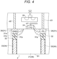
- Fig. 4 is a cross-sectional view of one pixel 2 of the photodetection device 1 according to the first embodiment.
- Fig. 4 is a diagonal cross-sectional view of each pixel 2 in Fig. 3 .
- An upper surface of Fig. 4 is a front surface, and a lower surface is a back surface, that is, a light incident surface S1. As described above, in the photodetection device 1 of Fig. 4 , light is incident from a back surface side.
- the pixel 2 in Fig. 4 has a structure in which the photoelectric conversion unit 21 and the pixel transistor 20 are stacked.
- the photoelectric conversion unit 21 is divided for each pixel 2 and is disposed in a silicon layer 36.
- a polysilicon layer 31 may be referred to as a conductor layer in the present specification
- an insulating layer 32 are stacked along the boundary region.
- the insulating layer 32 bonded to the polysilicon layer 31 and extending in a depth direction has a narrow width in a plane direction, it may be referred to as an STI layer 32 below.
- An interface between the polysilicon layer 31 and the STI layer 32 has a convex shape in a light incident surface S1 direction. With the convex shape, a part of the polysilicon layer 31 is covered with the STI layer 32 at the interface between the polysilicon layer 31 and the STI layer 32.
- the convex shape means that the polysilicon layer 31 has a step in the light incident surface S1 direction or has a convex surface portion at the interface.
- the polysilicon layer 31 has a protrusion 31p extending to an STI layer 32 side at the interface, and the interface has a step. An end portion of the protrusion 31p on the light incident surface S1 side is disposed inside STI layer 32.
- the protrusion 31p protruding from the polysilicon layer 31 is disposed so as to bite into the STI layer 32. Therefore, the STI layer 32 is disposed between a sidewall portion of the protrusion 31p and the silicon layer 36 in which the photoelectric conversion unit 21 is disposed.
- the polysilicon layer 31 in Fig. 4 has a first region 31a and a second region 31b along a pixel boundary region.
- the first region 31a is in contact with the silicon layer 36 in which the photoelectric conversion unit 21 is disposed.
- the second region 31b is bonded to the first region 31a and is disposed closer to the light incident surface S1 side than the first region 31a.
- the STI layer 32 is disposed between the second region 31b and the silicon layer 36.
- the polysilicon layer 31 is a conductive layer in conduction with the ground layer 30 or the floating diffusion layer 25. Two polysilicon layers 31 are provided for each pixel 2. One polysilicon layer 31 is in conduction with the ground layer 30, and the other polysilicon layer 31 is in conduction with the floating diffusion layer 25.
- the two polysilicon layers 31 provided in the pixel boundary region are shared by a plurality of pixels 2.
- the polysilicon layer 31 in conduction with the floating diffusion layer 25 is shared by the first pixel group including the four pixels 2
- the polysilicon layer 31 in conduction with the ground layer 30 is shared by the second pixel group including the four pixels 2.
- a boundary layer 33 is stacked on the light incident surface S1 side of the STI layer 32 along the boundary region of the plurality of photoelectric conversion units 21.
- the boundary layer 33 includes a polysilicon layer 34 or a fixed charge layer. A negative bias voltage is applied to the boundary layer 33. Thereby, a positive charge is induced on a surface of the boundary layer 33 at the time of light reception, and generation of a dark current and a white spot can be suppressed, and display quality can be improved.
- the boundary layer 33 is a through trench penetrating the silicon layer 36.
- impurities are dosed to the polysilicon layer 31 on a surface side opposite to the light incident surface S1 in order to make the polysilicon layer 31 conductive.
- the polysilicon layer 31 in conduction with the ground layer 30 and the polysilicon layer 31 in conduction with the floating diffusion layer 25 have different types of impurities to be dosed.
- the impurities When the impurities are dosed to the polysilicon layer 31, some of the dosed impurities are diffused into the silicon layer 36, and a diffusion layer is formed.
- the diffusion layer forms the diffusion capacitance.
- the transfer transistor 24 having the transfer gate TG and the other pixel transistors 20 are disposed in mutually different layers.
- the plurality of pixel transistors 20 is provided in the pixel 2, but an arrangement form of each pixel transistor 20 is arbitrary, and various modifications are conceivable.
- the photodetection device 1 having a stacked structure in which the substrate on which the pixel array unit 3 of Fig. 1 is formed and another substrate on which the vertical driving circuit 4, the column signal processing circuit 5, the horizontal driving circuit 6, the control circuit 8, and the like are formed are bonded in a stacking direction by Cu-Cu bonding or the like may be manufactured.
- Fig. 5 is a sectional view of the pixel 2 according to a comparative example.
- the same components as those in Fig. 4 are denoted by the same reference numerals.
- the cross-sectional shape of the interface between the polysilicon layer 31 and the STI layer 32 is different from that in Fig. 4 .
- the interface between the polysilicon layer 31 and the STI layer 32 in Fig. 5 is a flat surface, and the polysilicon layer 31 in Fig. 5 does not have the protrusion 31p as in Fig. 4 .
- Other structures are common to Figs. 4 and 5 .
- a volume of the polysilicon layer 31 in the pixel boundary region is smaller than that of the pixel 2 according to the present embodiment illustrated in Fig. 4 .
- the difference in volume between the polysilicon layers 31 in Figs. 4 and 5 will be described in more detail.
- Fig. 6 is a plan view near a bonding place between the polysilicon layers 31 and the STI layer 32 in Figs. 4 and 5 .
- Fig. 7A is a cross-sectional view taken along line A-A in Fig. 6 in the pixel 2 of Fig. 4
- Fig. 7B is a cross-sectional view taken along line B-B in Fig. 6 in the pixel 2 of Fig. 4 .
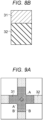
- Fig. 8A is a cross-sectional view taken along line A-A in Fig. 6 in the pixel 2 of Fig. 5
- Fig. 8B is a cross-sectional view taken along line B-B in Fig. 6 in the pixel 2 of Fig. 5 .
- the interface between the polysilicon layer 31 and the STI layer 32 is a flat surface, whereas in the pixel 2 according to the present embodiment, the interface between the polysilicon layer 31 and the STI layer 32 has the convex shape. Therefore, the volume of the polysilicon layer 31 according to the present embodiment is larger than the volume of the polysilicon layer 31 according to the comparative example.
- the polysilicon layer 31 functions as a conductor layer in conduction with the floating diffusion layer 25 or the ground layer 30. To cause the polysilicon layer 31 to function as a conductor layer, it is necessary to inject impurities into the polysilicon layer 31.
- the polysilicon layer 31 can incorporate more impurities therein than the STI layer 32.
- the interface between the polysilicon layer 31 and the STI layer 32 stacked in the pixel boundary region may have a convex shape on the light incident surface S1 side depending on conditions of a manufacturing process or the like.
- the volume of the polysilicon layer 31 increases, and the amount of impurities diffused from the sidewall portions of the polysilicon layer 31 and the STI layer 32 into the silicon layer 36 where the photoelectric conversion unit 21 is disposed can be suppressed.
- the shape of the interface between the polysilicon layer 31 and the STI layer 32 is not limited to those illustrated in Figs. 4 , 7A , and 7B , and various shapes are conceivable.
- Fig. 9A is a plan view according to a first specific example
- Fig. 9B is a cross-sectional view taken along line A-A in Fig. 9A
- Fig. 9C is a cross-sectional view taken along line B-B in Fig. 9A
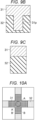
- Fig. 10A is a plan view according to a second specific example
- Fig. 10B is a cross-sectional view taken along line A-A in Fig. 10A
- Fig. 10C is a cross-sectional view taken along line B-B in Fig. 10A
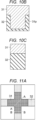
- Fig. 11A is a plan view according to a third specific example
- Fig. 11B is a cross-sectional view taken along line A-A in Fig.
- Fig. 11A is a plan view according to a fourth specific example
- Fig. 12B is a cross-sectional view taken along line A-A in Fig. 12A
- Fig. 12C is a cross-sectional view taken along line B-B in Fig. 12A .
- the first specific example and the second specific example include the columnar protrusion 31p protruding from a part of the polysilicon layer 31 to the STI layer 32, and the widths of the protrusions 31p are different from each other. Specifically, the width of the protrusion 31p in the second specific example is larger than that in the first specific example.
- the interface between the polysilicon layer 31 and the STI layer 32 has a convex shape.
- the interface of the polysilicon layer 31 has a convex shape in the light incident surface S1 direction
- the interface of the STI layer 32 has a concave shape in the plane direction opposite to the light incident surface S1.
- the fourth specific example includes a cross-shaped protrusion 31p protruding from a part of the polysilicon layer 31 to the STI layer 32, and the cross-sectional shape of the protrusion 31p in the plane direction is a twelve square shape as illustrated in Fig. 12A .
- the cross-sectional shapes of the protrusions 31p in the first specific example and the second specific example are circular as illustrated in Figs. 9A and 10A .
- Fig. 13 is a table comparing the comparative example illustrated in Figs. 8A and 8B with the first to fourth specific examples illustrated in Figs. 9A to 12C .
- Fig. 13 illustrates a volume ratio of the polysilicon layer 31, the interface shape between the polysilicon layer 31 and the STI layer 32, a relative ratio of the amount of impurities absorbed by the polysilicon layer 31, a relative ratio of the amount of impurities diffused into the silicon layer 36, and a relative value of a dosage of impurities dosed into the polysilicon layer 31 in the comparative example and the first to fourth specific examples.
- Fig. 13 illustrates the amount of impurities absorbed in the polysilicon layer 31 and the amount of impurities diffused into the silicon layer 36 in a case where the same amount (for example, 100) of impurities is dosed in the comparative example and the first to fourth specific examples.
- the volume of the polysilicon layer 31 increases in the order of the comparative example, the first specific example, the second specific example, the third specific example, and the fourth specific example. Furthermore, the amount of impurities absorbed in the polysilicon layer 31 increases in the order of the comparative example, the first specific example, the second specific example, the third specific example, and the fourth specific example. Moreover, the amount of impurities diffused into the silicon layer 36 decreases in the order of the comparative example, the first specific example, the second specific example, the third specific example, and the fourth specific example.
- a length L1 (see Fig. 7B ) of the protrusion 31p of the polysilicon layer 31 in the stacking direction is desirably 10 nm or more, for example.
- a width L2 (see Fig. 7B ) of the STI layer 32 disposed between the sidewall portion of the protrusion 31p and the silicon layer 36 is desirably 20 nm or more, for example.
- Fig. 4 illustrates an example in which the boundary layer 33 including the polysilicon layer 34 is disposed on the light incident surface S1 side of the STI layer 32, but the boundary layer 33 may be a fixed charge layer 35 instead of the polysilicon layer 34.
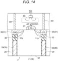
- Fig. 14 is a cross-sectional view of the pixel 2 including the boundary layer 33 having the fixed charge layer 35.
- the boundary layer 33 bonded to the STI layer 32 has a two-layer structure including the fixed charge layer 35 and an insulating layer 29.
- the fixed charge is a charge having the same polarity as a read charge.
- the fixed charge layer 35 Since a charge having a polarity opposite to the fixed charge is induced in the fixed charge layer 35, it is possible to suppress generation of a noise charge having the same polarity as the read charge in the vicinity of the pixel boundary.
- a material of the fixed charge layer 35 for example, Hf (hafnium), Ta (tantalum), Ti (titanium), or the like is used.
- Figs. 4 and 14 illustrate examples in which the end portion of the protrusion 31p of the polysilicon layer 31 on the light incident surface S1 side is provided inside the STI layer 32.
- the end portion of the protrusion 31p may extend to the vicinity of the boundary region between the STI layer 32 and the boundary layer 33.
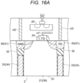
- Figs. 16A and 16B are cross-sectional views of the pixel 2 in the case where the interface between the polysilicon layer 31 and the STI layer 32 has a convex shape as illustrated in Fig. 11 .
- Fig. 16A illustrates an example in which the boundary layer 33 includes the polysilicon layer 34
- Fig. 16B illustrates an example in which the boundary layer 33 includes the fixed charge layer 35.
- the interface between the polysilicon layer 31 and the STI layer 32 in Figs. 16A and 16B has a convex shape, it is possible to increase the volume of the polysilicon layer 31 and to reduce the amount of impurities diffused into the silicon layer 36 as compared with the case of a flat surface.
- the polysilicon layer 31 and the STI layer (insulating layer) 32 are formed along the boundary region of the photoelectric conversion unit 21, and the interface between the polysilicon layer 31 and the STI layer 32 has a convex shape in the light incident surface S1 direction.
- the polysilicon layer 31 is doped with impurities for being made conductive, but much of the doped impurities are absorbed by the polysilicon layer 31.
- the volume of the polysilicon layer 31 is larger, and the impurities diffused from the sidewall portions of the polysilicon layer 31 and the STI layer 32 into the silicon layer 36 where the photoelectric conversion unit 21 is disposed can be suppressed. Thereby, the electric field does not change sharply in the vicinity of the pixel boundary of the photoelectric conversion unit 21, and the electric field design of the photoelectric conversion unit 21 becomes easy.
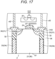
- Fig. 17 is a cross-sectional view of one pixel 2 of a photodetection device 1 according to a second embodiment.
- components common to those in Fig. 4 are denoted by the same reference numerals, and differences will be mainly described below.
- a cross-sectional structure of a polysilicon layer 31 and an insulating layer (STI layer) 32 in a boundary region is different from that in Fig. 4 .
- the boundary region of Fig. 17 at least a part of the polysilicon layer 31 is disposed so as to be in contact with a silicon layer 36, similarly to the boundary region of Fig. 4 .
- the polysilicon layer 31 in Fig. 17 has a step portion 31D in contact with the silicon layer 36.
- the step portion 31D indicates that the polysilicon layer 31 has a discontinuous sidewall surface.
- the polysilicon layer 31 has two discontinuous sidewall surfaces. A corner connecting a surface connecting the two discontinuous sidewall surfaces and each sidewall surface may have an acute angle or may be rounded.
- the silicon layer 36 is a layer in which a photoelectric conversion unit 21 is disposed.
- the step portion 31D of the polysilicon layer 31 is disposed along an end surface of the silicon layer 36 on a surface side opposite to a light incident surface S1. That is, a horizontal length of the polysilicon layer 31 above the end face of the silicon layer 36 is longer than the horizontal length of the polysilicon layer 31 below the end face of the silicon layer 36.
- the sidewall surface of the polysilicon layer 31 and the sidewall surface of the insulating layer 32 are flush with each other, and both sidewall surfaces are disposed so as to be in contact with the silicon layer 36.
- a boundary layer 33 is disposed closer to the light incident surface side than the insulating layer 32 in the boundary region of Fig. 17 , similarly to Fig. 4 .
- the boundary layer 33 includes a polysilicon layer 34 or a fixed charge layer. A negative bias voltage is applied to the boundary layer 33.
- the photodetection device 1 of Fig. 17 is different from the photodetection device 1 of Fig. 4 in that the sidewall surface of the polysilicon layer 31 and the sidewall surface of the insulating layer 32 in the boundary region are brought into contact with the silicon layer 36.
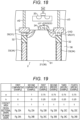
- Fig. 18 is a cross-sectional view of one pixel 2 of the photodetection device 1 according to a modification of the second embodiment.
- components common to those in Fig. 17 are denoted by the same reference numerals, and differences will be mainly described below.
- the photodetection device 1 of Fig. 18 is different from that of Fig. 17 in the structure of the step portion 31D of the polysilicon layer 31 in the boundary region.
- the step portion 31D in Fig. 18 is disposed closer to the light incident surface S1 than the end surface of the silicon layer 36 on the surface side opposite to the light incident surface S1. That is, in Fig. 18 , the horizontal length of the polysilicon layer 31 between the step portion 31D and the end surface of the silicon layer 36 is longer than the horizontal length of the polysilicon layer 31 on the light incident surface side with respect to the step portion 31D.
- the sidewall surface of the polysilicon layer 31 and the sidewall surface of the insulating layer 32 on the light incident surface side with respect to the step portion 31D are flush with each other, and both sidewall surfaces are disposed so as to be in contact with the silicon layer 36.
- the cross-sectional structure of the boundary region of each pixel 2 in the photodetection device 1 according to the second embodiment is not necessarily limited to that illustrated in Fig. 17 or 18 , and various modifications are assumed.
- Fig. 19 is a table illustrating characteristics of representative shapes of the photodetection device 1 according to the second embodiment.
- Fig. 19 illustrates characteristics of the shapes of the photodetection device 1 according to first and second comparative examples and first to fourth specific examples.
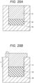
- Fig. 20A is a view illustrating the cross-sectional structure of the boundary region according to the first and second comparative examples.
- Fig. 20B is a view illustrating the cross-sectional structure of the boundary region according to the first and second specific examples.
- Fig. 20C is a view illustrating the cross-sectional structure of the boundary region according to the third and fourth specific examples.
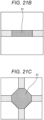
- Fig. 21A is a plan view of the boundary region according to the first comparative example, and illustrates an example of a cross shape.
- Fig. 21A is a plan view of the boundary region according to the first comparative example, and illustrates an example of a cross shape.
- Fig. 21A is a plan view of the boundary region according to the first comparative
- FIG. 21B is a plan view of the boundary region according to the second comparative example, the second specific example, and the fourth specific example, and illustrates an example of a rectangular shape.
- Fig. 21C is a plan view of the boundary region according to the first specific example and the third specific example, and illustrates an example of an octagonal shape.
- a parameter a in Fig. 19 is a parameter related to the length of the polysilicon layer 31 in a depth direction from the end face of the silicon layer 36 on the surface side opposite to the light incident surface S1.
- a parameter b is a parameter related to the horizontal length of the polysilicon layer 31 at the step portion 31D.
- a contact area is an area of a contact interface between the polysilicon layer 31 and the insulating layer 32.
- values of the parameters a and b are represented by a ratio in which a sum of the lengths of the parameters a and b is 1.
- the values of the parameters a and b are an example, and are not limited to the values in Fig. 19 .
- Fig. 19 illustrates characteristics of the cross-sectional shapes and the planar shapes of the boundary regions according to the first to fourth specific examples, but the cross-sectional shape and the planar shape of the boundary region of the photodetection device 1 according to the second embodiment are not limited to those illustrated in Fig. 19 .
- the step portion 31D is provided in the polysilicon layer 31 in the boundary region so that the step portion 31D is in contact with the silicon layer 36, the area of the polysilicon layer 31 in contact with the silicon layer 36 can be increased. Thereby, the volume of the polysilicon layer 31 increases, and the impurities diffused from the sidewall portions of the polysilicon layer 31 and the insulating layer (STI layer) 32 into the silicon layer 36 where the photoelectric conversion unit 21 is disposed can be suppressed. Therefore, an electric field does not change sharply near the boundary of the pixel 2 of the photoelectric conversion unit 21, and electric field design of the photoelectric conversion unit 21 becomes easy.
- a third embodiment is provided with a vertical electrode extending from a transfer electrode in a depth direction of a silicon layer 36 in a pixel 2, and efficiently collects a photoelectrically converted charge using the vertical electrode and easily transfers the charge from the transfer electrode and the vertical electrode to a floating diffusion layer 25.
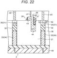
- Fig. 22 is a cross-sectional view of one pixel 2 of a photodetection device 1 according to the third embodiment.
- components common to those in Fig. 4 are denoted by the same reference numerals, and differences will be mainly described below.
- the pixel 2 in Fig. 22 includes the floating diffusion layer 25 (floating gate) or a ground layer 30 disposed along a boundary region of the pixel 2.
- the floating diffusion layer 25 and the ground layer 30 include a polysilicon layer 31, and an insulating layer (STI layer) 32 is disposed on a light incident surface side with respect to the polysilicon layer 31.
- a boundary layer 33 is disposed on the light incident surface side with respect to the insulating layer 32 in the boundary region.
- the boundary layer 33 includes a polysilicon layer 34 or a fixed charge layer.
- a sidewall surface of the polysilicon layer 31 constituting the floating diffusion layer 25 and a sidewall surface of the insulating layer 32 are flush with each other and are in contact with the silicon layer 36.
- N-type impurities are implanted into the polysilicon layer 31.
- the N-type impurities are diffused from the sidewall surface of the polysilicon layer 31 toward the silicon layer 36 to form an N-type diffusion region 42.
- the N-type diffusion region 42 has a self-alignment structure that diffuses from the sidewall surface of the polysilicon layer 31 to the silicon layer 36 in the boundary region.
- the N-type diffusion region 42 disposed in the sidewall portion of the floating diffusion layer 25 is referred to as a side contact structure.
- a transfer electrode 43 is disposed on an end surface of the silicon layer 36 on a surface side opposite to a light incident surface S1, and a vertical electrode 44 extends from the transfer electrode 43 in the depth direction of the silicon layer 36.
- a sidewall portion 48 is disposed along sidewall surfaces of the transfer electrode 43 and the vertical electrode 44.
- the sidewall portion 48 includes a silicon nitride layer 46. More specifically, the sidewall portion 48 has a laminated structure in which a silicon oxide film 45, a silicon nitride film 46, and a silicon oxide film 47 are stacked from the sidewall surfaces of the transfer electrode 43 and the vertical electrode 44 toward the N-type diffusion region 42.
- the sidewall portion 48 is disposed to face an N-type impurity region of the floating diffusion layer 25. Thereby, a charge transferred to the transfer electrode 43 via the vertical electrode 44 is transferred to the floating diffusion layer 25 via the sidewall portion 48 and the N-type impurity region.
- Fig. 23 is a sectional view of a pixel 101 according to a comparative example.
- the sidewall portion 48 is not disposed near the corner portion of the transfer electrode 43 and the vertical electrode 44 in Fig. 23 . For this reason, the electric field of the sidewall surface of the vertical electrode 44 becomes large, the electric field design of the silicon layer 36 becomes difficult, and the pixel 2 cannot be downsized.
- the pixel 2 in Fig. 22 is assumed to employ a manufacturing method in which a trench (STI) is formed in the silicon layer 36 from the surface side opposite to the light incident surface S1, and the boundary layer 33, the insulating layer 32, and the polysilicon layer 31 are sequentially formed.
- a manufacturing method in which a trench is formed in the boundary region from the light incident surface (back surface) side and each layer is formed may be employed.
- Fig. 24 is a cross-sectional view of the pixel 2 prepared by forming a trench 38 from the light incident surface side.
- the trench 38 in Fig. 24 is formed so as to penetrate the silicon layer 36 from the light incident surface (back surface) side in the boundary region.
- the polysilicon layer 31, the insulating layer (STI layer) 32, and the boundary layer 33 are stacked in this order from the surface side opposite to the light incident surface S1.
- a color filter layer 49 is disposed on the light incident surface side of the silicon layer 36.
- an on-chip lens layer (not illustrated) may be disposed on the light incident surface side of the color filter layer 49.
- the boundary layer 33 in Fig. 24 may be an insulating layer of SiO 2 or the like, or may include a light shielding member of aluminum (Al), tungsten (W), platinum (Pt), or the like. Furthermore, voids may be included in at least a part of the boundary layer 33. By forming the boundary layer 33 as a light shielding member, it is possible to prevent incidence of light from the adjacent pixel 2 and to improve performance of color mixture prevention.
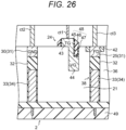
- Fig. 26 is a cross-sectional view of the pixel 2 according to a modification of Fig. 24 .
- Fig. 26 is different from Fig. 24 in the structure of the boundary layer 33.
- the boundary layer 33 in Fig. 26 has, for example, the polysilicon layer 31 or the fixed charge film, and a negative bias voltage is applied thereto. Thereby, pinning on the sidewall surface of the boundary layer 33 can be enhanced, and dark current can be suppressed.
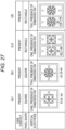
- Fig. 27 is a table summarizing characteristics of a plurality of representative specific examples of the vertical electrode 44.
- Fig. 27(a) is a plan view of the pixel 2 according to the first specific example.
- Fig. 27(a) illustrates arrangement locations of the floating diffusion layer 25, the transfer electrode 43, and the vertical electrode 44 in the adjacent four pixels 2.
- the transfer electrode 43 and the vertical electrode 44 each having a triangular planar shape are disposed to be shifted in each pixel 2.
- the floating diffusion layer 25 is disposed in the central boundary region of the total of four pixels 2, two in each of vertical and horizontal directions.
- the transfer electrode 43 and the vertical electrode 44 are symmetrically disposed in each of the four pixels 2 around the floating diffusion layer 25.
- the floating diffusion layer 25 in Fig. 27(a) has a side contact structure as illustrated in Fig. 24 .
- Fig. 27(b) is a plan view of the pixel 2 according to the second specific example.
- the direction of the transfer electrode 43 and the vertical electrode 44 of each pixel 2 is different from that in Fig. 27(a) , but is common to Fig. 27(a) in that the transfer electrode 43 and the vertical electrode 44 of each pixel 2 are symmetrically disposed with respect to the floating diffusion layer 25, and the transfer electrode 43 and the vertical electrode 44 have the sidewall portion 48.
- Fig. 27(c) is a plan view of the pixel 2 according to the third specific example.
- Fig. 27(c) illustrates an example of a phase difference detection pixel 2.
- the phase difference detection pixel 2 detects a phase difference using a left (L) pixel and a right (R) pixel as a set.
- Fig. 27(c) illustrates an example in which two phase difference detection pixels 2 share the floating diffusion layer 25. This example is common to Fig. 27(a) in that the transfer electrode 43 and the vertical electrode 44 are symmetrically disposed with respect to the floating diffusion layer 25, and the transfer electrode 43 and the vertical electrode 44 have the sidewall portion 48.
- Fig. 27(d) is a plan view of the pixel 2 according to the fourth specific example.
- Fig. 27(d) illustrates an example of the phase difference detection pixel 2 similarly to Fig. 27(c) , and the direction of the transfer electrode 43 and the vertical electrode 44 is different from that in Fig. 27(c) .
- Figs. 27(a) to 27(d) illustrate the examples in which the planar shapes of the transfer electrode 43 and the vertical electrode 44 are triangular, but the planar shapes of the transfer electrode 43 and the vertical electrode 44 are arbitrary. Furthermore, the numbers of transfer electrodes 43 and vertical electrodes 44 disposed in one pixel 2 are also arbitrary.
- Fig. 28 is a table summarizing characteristics of a plurality of representative modifications of the vertical electrode 44.
- Fig. 28(a) is a plan view of the pixel 2 according to the first modification.
- the floating diffusion layer 25 is disposed at the center of four adjacent pixels 2.
- the floating diffusion layer 25 has a side contact structure.
- the transfer electrode 43 having a square planar shape and the vertical electrode 44 having a circular planar shape are disposed to be shifted from each other, and the sidewall portion 48 is disposed on the sidewall surfaces of the transfer electrode 43 and the vertical electrode 44.
- the transfer electrode 43 and the vertical electrode 44 of each pixel 2 are symmetrically disposed with respect to the floating diffusion layer 25.
- Fig. 28(b) is a plan view of the pixel 2 according to the second modification.
- Each pixel 2 in Fig. 28(b) has two transfer electrodes 43 and two vertical electrodes 44.
- the two transfer electrodes 43 in the pixel 2 are disposed in a diagonal direction, and the two vertical electrodes 44 are disposed to face each other.
- Fig. 28(c) is a plan view of the pixel 2 according to the third modification.
- Fig. 28(c) illustrates an example of the phase difference detection pixel 2.
- Figs. 27(c) and 27(d) are common in that the two phase difference detection pixels 2 share the floating diffusion layer 25. Each phase difference detection pixel 2 is symmetrically disposed with respect to the floating diffusion layer 25.
- Fig. 28(d) is a plan view of the pixel 2 according to the fourth modification.
- Fig. 28(d) illustrates an example of the phase difference detection pixel 2, similarly to Fig. 28(c) .
- twice as many transfer electrodes 43 and vertical electrodes 44 as those in Fig. 28(c) are disposed in each pixel 2.
- This example is common to Fig. 28(c) in that each of the phase difference detection pixels 2 is symmetrically disposed with respect to the floating diffusion layer 25.
- Figs. 27(a) to 27(d) and Figs. 28(a) to 28(d) various variations can be assumed in the planar shapes, the arrangement locations, the numbers of arrangements, and the arrangement directions of the transfer electrode 43 and the vertical electrode 44.
- the silicon layer 36 in which the vertical electrode 44 is formed a generation ratio of unbonded dangling bonds is different depending on a plane orientation, and a generation frequency of dark current is also different. Therefore, the plane orientation of silicon may be taken into consideration when forming the boundary layer 33 with the vertical electrode 44.
- Fig. 29A is a plan view of the pixel 2 according to the fifth modification.
- Fig. 29A illustrates an example in which the plane orientations of the vertical electrode 44 and the boundary layer 33 are matched with each other.
- Fig. 29A illustrates an example in which the planar shape of the vertical electrode 44 is rectangular.
- both the plane orientation of the vertical electrode 44 and the plane orientation of the boundary layer 33 are set to a (100) plane.
- the (100) plane has a smaller ratio of dangling bonds and a smaller generation ratio of dark current than other plane orientations, for example, a (110) plane. Therefore, by setting both the plane orientation of the vertical electrode 44 and the plane orientation of the boundary layer 33 to the (100) plane, dark current in the boundary region can be suppressed.
- Fig. 29B is a plan view of the pixel 2 according to the sixth modification.
- Fig. 29B is different from Fig. 29A in that the planar shape of the vertical electrode 44 is triangular, but is common to Fig. 29A in that the plane orientations of the vertical electrode 44 and the boundary layer 33 are set to, for example, the (100) plane.
- the N-type diffusion region 42 diffused in a self-alignment manner from the floating diffusion layer 25 including the polysilicon layer 31 disposed in the boundary region of the pixel 2 to the periphery is provided, the vertical electrode 44 extending in the depth direction from the transfer electrode 43 disposed on the end surface of the silicon layer 36 on the surface side opposite to the light incident surface S1 is provided, and the sidewall portion 48 is disposed on the sidewall surfaces of the transfer electrode 43 and the vertical electrode 44.
- the photoelectric conversion unit 21 and the pixel circuit constituting each pixel 2 of the photodetection device 1 according to the above-described first to third embodiments may be disposed on the same substrate or may be disposed on different substrates.
- Fig. 30A is a cross-sectional view of one pixel 2 of a photodetection device 1 according to a fourth embodiment.
- a substrate 51 on which a photoelectric conversion unit is disposed and a substrate 52 on which a pixel circuit is disposed are separately provided, and these substrates 51 and 52 are stacked.
- a boundary region of the pixel 2 in Fig. 30A has a structure in which a polysilicon layer 31, an insulating layer (STI layer) 32, and a boundary layer 33 are stacked, for example, similarly to Fig. 24 . Furthermore, a transfer electrode 43 is disposed on an end surface of a silicon layer 36 on a surface side opposite to a light incident surface S1, and a vertical electrode 44 extends from the transfer electrode 43 in a depth direction of the silicon layer 36. A length of the vertical electrode 44 in the depth direction is arbitrary, and for example, the vertical electrode 44 may extend to a position deeper than an interface between the insulating layer 32 and the boundary layer 33, or the vertical electrode 44 may extend to a position shallower than the above-described interface.
- Contacts ct2 and ct3 extending upward are connected to the polysilicon layer 31 in the boundary region. Similarly, a contact ct1 extending upward is connected to the transfer electrode 43.
- a pixel 2 transistor is disposed in the pixel circuit.
- the pixel 2 transistor includes an amplification transistor, a reset transistor, a selection transistor, and the like (not illustrated).
- the pixel 2 transistor may include a fin gate or a planar gate.
- a contact ct4 extending upward is connected to the fin gate or the planar gate of the pixel 2 transistor.
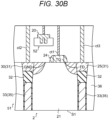
- Fig. 30B is a cross-sectional view of the pixel 2 according to a modification of Fig. 30A .
- the structure of the boundary layer 33 is the same as that in Fig. 26 .
- Figs. 30A and 30B are merely examples.
- the polysilicon layer 31 in the boundary region may have a protrusion 31p, similarly to Fig. 4 , or may have a convex surface, similarly to Fig. 16A .
- the vertical electrode 44 in each pixel 2 of the photodetection device 1 according to the fourth embodiment may have any structure of Figs. 28(a) to 28(d) , Figs. 29A to 29D, and Figs. 30A and 30B . Moreover, the vertical electrode 44 is not necessarily required, and may be omitted.
- the photoelectric conversion unit and the pixel circuit are disposed and stacked on the separate substrates, a volume of the photoelectric conversion unit for each pixel 2 can be increased, and sensitivity can be improved. Furthermore, the pixel 2 can be miniaturized. Moreover, by stacking a plurality of substrates, a chip can be downsized.
- the technology according to the present disclosure can be applied to various products.
- the technology according to the present disclosure may also be implemented as a device mounted on any kind of mobile body such as an automobile, an electric automobile, a hybrid electric automobile, a motorcycle, a bicycle, a personal mobility, an airplane, a drone, a ship, a robot, a construction machine, an agricultural machine (tractor), or the like.
- Fig. 31 is a block diagram illustrating an example of schematic configuration of a vehicle control system 7000 as an example of a mobile body control system to which the technology according to an embodiment of the present disclosure can be applied.
- the vehicle control system 7000 includes a plurality of electronic control units connected to each other via a communication network 7010.
- the vehicle control system 7000 includes a driving system control unit 7100, a body system control unit 7200, a battery control unit 7300, an outside-vehicle information detecting unit 7400, an in-vehicle information detecting unit 7500, and an integrated control unit 7600.
- the communication network 7010 connecting the plurality of control units to each other may, for example, be a vehicle-mounted communication network compliant with an arbitrary standard such as controller area network (CAN), local interconnect network (LIN), local area network (LAN), FlexRay (registered trademark), or the like.
- CAN controller area network
- LIN local interconnect network
- LAN local area network
- FlexRay registered trademark
- Each of the control units includes: a microcomputer that performs arithmetic processing according to various kinds of programs; a storage section that stores the programs executed by the microcomputer, parameters used for various kinds of operations, or the like; and a driving circuit that drives various kinds of control target devices.
- Each of the control units further includes: a network interface (I/F) for performing communication with other control units via the communication network 7010; and a communication I/F for performing communication with a device, a sensor, or the like within and without the vehicle by wire communication or radio communication.
- I/F network interface
- control unit 7600 as a functional configuration of the integrated control unit 7600, a microcomputer 7610, a general-purpose communication I/F 7620, a dedicated communication I/F 7630, a positioning section 7640, a beacon receiving section 7650, an in-vehicle device I/F 7660, a sound/image output section 7670, a vehicle-mounted network I/F 7680, and a storage section 7690 are illustrated.
- the other control units similarly include a microcomputer, a communication I/F, a storage section, and the like.
- the driving system control unit 7100 controls the operation of devices related to the driving system of the vehicle in accordance with various kinds of programs.
- the driving system control unit 7100 functions as a control device for a driving force generating device for generating the driving force of the vehicle, such as an internal combustion engine, a driving motor, or the like, a driving force transmitting mechanism for transmitting the driving force to wheels, a steering mechanism for adjusting the steering angle of the vehicle, a braking device for generating the braking force of the vehicle, and the like.
- the driving system control unit 7100 may have a function as a control device of an antilock brake system (ABS), electronic stability control (ESC), or the like.
- ABS antilock brake system
- ESC electronic stability control
- the driving system control unit 7100 is connected with a vehicle state detecting section 7110.
- the vehicle state detecting section 7110 includes at least one of a gyro sensor that detects the angular velocity of axial rotational movement of a vehicle body, an acceleration sensor that detects the acceleration of the vehicle, and sensors for detecting an amount of operation of an accelerator pedal, an amount of operation of a brake pedal, the steering angle of a steering wheel, an engine speed or the rotational speed of wheels, and the like.
- the driving system control unit 7100 performs arithmetic processing using a signal input from the vehicle state detecting section 7110, and controls the internal combustion engine, the driving motor, an electric power steering device, the brake device, and the like.
- the body system control unit 7200 controls the operation of various kinds of devices provided to the vehicle body in accordance with various kinds of programs.
- the body system control unit 7200 functions as a control device for a keyless entry system, a smart key system, a power window device, or various kinds of lamps such as a headlamp, a backup lamp, a brake lamp, a turn signal, a fog lamp, or the like.
- radio waves transmitted from a mobile device as an alternative to a key or signals of various kinds of switches can be input to the body system control unit 7200.
- the body system control unit 7200 receives these input radio waves or signals, and controls a door lock device, the power window device, the lamps, or the like of the vehicle.
- the battery control unit 7300 controls a secondary battery 7310, which is a power supply source for the driving motor, in accordance with various kinds of programs.
- the battery control unit 7300 is supplied with information about a battery temperature, a battery output voltage, an amount of charge remaining in the battery, or the like from a battery device including the secondary battery 7310.
- the battery control unit 7300 performs arithmetic processing using these signals, and performs control for regulating the temperature of the secondary battery 7310 or controls a cooling device provided to the battery device or the like.
- the outside-vehicle information detecting unit 7400 detects information about the outside of the vehicle including the vehicle control system 7000.
- the outside-vehicle information detecting unit 7400 is connected with at least one of an imaging section 7410 and an outside-vehicle information detecting section 7420.
- the imaging section 7410 includes at least one of a time-of-flight (ToF) camera, a stereo camera, a monocular camera, an infrared camera, and other cameras.
- ToF time-of-flight
- the outside-vehicle information detecting section 7420 includes at least one of an environmental sensor for detecting current atmospheric conditions or weather conditions and a peripheral information detecting sensor for detecting another vehicle, an obstacle, a pedestrian, or the like on the periphery of the vehicle including the vehicle control system 7000.
- the environmental sensor may be at least one of a rain drop sensor detecting rain, a fog sensor detecting a fog, a sunshine sensor detecting a degree of sunshine, and a snow sensor detecting a snowfall.
- the peripheral information detecting sensor may be at least one of an ultrasonic sensor, a radar device, and a LIDAR device (Light detection and Ranging device, or Laser imaging detection and ranging device).
- Each of the imaging section 7410 and the outside-vehicle information detecting section 7420 may be provided as an independent sensor or device, or may be provided as a device in which a plurality of sensors or devices are integrated.
- FIG. 32 illustrates an example of installation positions of the imaging section 7410 and the outside-vehicle information detecting section 7420.
- Imaging sections 7910, 7912, 7914, 7916, and 7918 are, for example, disposed at at least one of positions on a front nose, sideview mirrors, a rear bumper, and a back door of the vehicle 7900 and a position on an upper portion of a windshield within the interior of the vehicle.
- the imaging section 7910 provided to the front nose and the imaging section 7918 provided to the upper portion of the windshield within the interior of the vehicle obtain mainly an image of the front of the vehicle 7900.
- the imaging sections 7912 and 7914 provided to the sideview mirrors obtain mainly an image of the sides of the vehicle 7900.
- the imaging section 7916 provided to the rear bumper or the back door obtains mainly an image of the rear of the vehicle 7900.
- the imaging section 7918 provided to the upper portion of the windshield within the interior of the vehicle is used mainly to detect a preceding vehicle, a pedestrian, an obstacle, a signal, a traffic sign, a lane, or the like.
- the outside-vehicle information detecting unit 7400 makes the imaging section 7410 image an image of the outside of the vehicle, and receives imaged image data.
- the outside-vehicle information detecting unit 7400 receives detection information from the outside-vehicle information detecting section 7420 connected to the outside-vehicle information detecting unit 7400.
- the outside-vehicle information detecting section 7420 is an ultrasonic sensor, a radar device, or a LIDAR device
- the outside-vehicle information detecting unit 7400 transmits an ultrasonic wave, an electromagnetic wave, or the like, and receives information of a received reflected wave.
- the outside-vehicle information detecting unit 7400 may perform processing of detecting an object such as a human, a vehicle, an obstacle, a sign, a character on a road surface, or the like, or processing of detecting a distance thereto.
- the outside-vehicle information detecting unit 7400 may perform environment recognition processing of recognizing a rainfall, a fog, road surface conditions, or the like on the basis of the received information.
- the outside-vehicle information detecting unit 7400 may calculate a distance to an object outside the vehicle on the basis of the received information.
- the in-vehicle information detecting unit 7500 may calculate a degree of fatigue of the driver or a degree of concentration of the driver, or may determine whether the driver is dozing.
- the in-vehicle information detecting unit 7500 may subject an audio signal obtained by the collection of the sound to processing such as noise canceling processing or the like.
- the integrated control unit 7600 controls general operation within the vehicle control system 7000 in accordance with various kinds of programs.
- the integrated control unit 7600 is connected with an input section 7800.
- the input section 7800 is implemented by a device capable of input operation by an occupant, such, for example, as a touch panel, a button, a microphone, a switch, a lever, or the like.
- the integrated control unit 7600 may be supplied with data obtained by voice recognition of voice input through the microphone.
- the input section 7800 may, for example, be a remote control device using infrared rays or other radio waves, or an external connecting device such as a mobile telephone, a personal digital assistant (PDA), or the like that supports operation of the vehicle control system 7000.
- the input section 7800 may be, for example, a camera.
- an occupant can input information by gesture.
- data may be input which is obtained by detecting the movement of a wearable device that an occupant wears.
- the input section 7800 may, for example, include an input control circuit or the like that generates an input signal on the basis of information input by an occupant or the like using the above-described input section 7800, and which outputs the generated input signal to the integrated control unit 7600.
- An occupant or the like inputs various kinds of data or gives an instruction for processing operation to the vehicle control system 7000 by operating the input section 7800.
- the storage section 7690 may include a read only memory (ROM) that stores various kinds of programs executed by the microcomputer and a random access memory (RAM) that stores various kinds of parameters, operation results, sensor values, or the like.
- ROM read only memory
- RAM random access memory
- the storage section 7690 may be implemented by a magnetic storage device such as a hard disc drive (HDD) or the like, a semiconductor storage device, an optical storage device, a magneto-optical storage device, or the like.
- the general-purpose communication I/F 7620 is a communication I/F used widely, which communication I/F mediates communication with various apparatuses present in an external environment 7750.
- the general-purpose communication I/F 7620 may implement a cellular communication protocol such as global system for mobile communications (GSM (registered trademark)), worldwide interoperability for microwave access (WiMAX (registered trademark)), long term evolution (LTE (registered trademark)), LTE-advanced (LTE-A), or the like, or another wireless communication protocol such as wireless LAN (referred to also as wireless fidelity (Wi-Fi (registered trademark)), Bluetooth (registered trademark), or the like.
- GSM global system for mobile communications
- WiMAX worldwide interoperability for microwave access
- LTE registered trademark
- LTE-advanced LTE-advanced
- WiFi wireless fidelity
- Bluetooth registered trademark
- the dedicated communication I/F 7630 is a communication I/F that supports a communication protocol developed for use in vehicles.
- the dedicated communication I/F 7630 may implement a standard protocol such, for example, as wireless access in vehicle environment (WAVE), which is a combination of institute of electrical and electronic engineers (IEEE) 802.11p as a lower layer and IEEE 1609 as a higher layer, dedicated short range communications (DSRC), or a cellular communication protocol.
- WAVE wireless access in vehicle environment
- IEEE institute of electrical and electronic engineers
- DSRC dedicated short range communications
- the dedicated communication I/F 7630 typically carries out V2X communication as a concept including one or more of communication between a vehicle and a vehicle (Vehicle to Vehicle), communication between a road and a vehicle (Vehicle to Infrastructure), communication between a vehicle and a home (Vehicle to Home), and communication between a pedestrian and a vehicle (Vehicle to Pedestrian).
- the positioning section 7640 performs positioning by receiving a global navigation satellite system (GNSS) signal from a GNSS satellite (for example, a GPS signal from a global positioning system (GPS) satellite), and generates positional information including the latitude, longitude, and altitude of the vehicle.
- GNSS global navigation satellite system
- GPS global positioning system
- the positioning section 7640 may identify a current position by exchanging signals with a wireless access point, or may obtain the positional information from a terminal such as a mobile telephone, a personal handyphone system (PHS), or a smart phone that has a positioning function.
- the beacon receiving section 7650 receives a radio wave or an electromagnetic wave transmitted from a radio station installed on a road or the like, and thereby obtains information about the current position, congestion, a closed road, a necessary time, or the like.
- the function of the beacon receiving section 7650 may be included in the dedicated communication I/F 7630 described above.
- the in-vehicle device I/F 7660 is a communication interface that mediates connection between the microcomputer 7610 and various in-vehicle devices 7760 present within the vehicle.
- the in-vehicle device I/F 7660 may establish wireless connection using a wireless communication protocol such as wireless LAN, Bluetooth (registered trademark), near field communication (NFC), or wireless universal serial bus (WUSB).
- a wireless communication protocol such as wireless LAN, Bluetooth (registered trademark), near field communication (NFC), or wireless universal serial bus (WUSB).
- WUSB wireless universal serial bus
- the in-vehicle device I/F 7660 may establish wired connection by universal serial bus (USB), high-definition multimedia interface (HDMI (registered trademark)), mobile high-definition link (MHL), or the like via a connection terminal (and a cable if necessary) not depicted in the figures.
- USB universal serial bus
- HDMI high-definition multimedia interface
- MHL mobile high-definition link
- the in-vehicle devices 7760 may, for example, include at least one of a mobile device and a wearable device possessed by an occupant and an information device carried into or attached to the vehicle.
- the in-vehicle devices 7760 may also include a navigation device that searches for a path to an arbitrary destination.
- the in-vehicle device I/F 7660 exchanges control signals or data signals with these in-vehicle devices 7760.
- the vehicle-mounted network I/F 7680 is an interface that mediates communication between the microcomputer 7610 and the communication network 7010.
- the vehicle-mounted network I/F 7680 transmits and receives signals or the like in conformity with a predetermined protocol supported by the communication network 7010.
- the microcomputer 7610 of the integrated control unit 7600 controls the vehicle control system 7000 in accordance with various kinds of programs on the basis of information obtained via at least one of the general-purpose communication I/F 7620, the dedicated communication I/F 7630, the positioning section 7640, the beacon receiving section 7650, the in-vehicle device I/F 7660, and the vehicle-mounted network I/F 7680.
- the microcomputer 7610 may calculate a control target value for the driving force generating device, the steering mechanism, or the braking device on the basis of the obtained information about the inside and outside of the vehicle, and output a control command to the driving system control unit 7100.
- the microcomputer 7610 may perform cooperative control intended to implement functions of an advanced driver assistance system (ADAS) which functions include collision avoidance or shock mitigation for the vehicle, following driving based on a following distance, vehicle speed maintaining driving, a warning of collision of the vehicle, a warning of deviation of the vehicle from a lane, or the like.
- ADAS advanced driver assistance system
- the microcomputer 7610 may perform cooperative control intended for automated driving, which makes the vehicle to travel automatedly without depending on the operation of the driver, or the like, by controlling the driving force generating device, the steering mechanism, the braking device, or the like on the basis of the obtained information about the surroundings of the vehicle.
- the microcomputer 7610 may generate three-dimensional distance information between the vehicle and an object such as a surrounding structure, a person, or the like, and generate local map information including information about the surroundings of the current position of the vehicle, on the basis of information obtained via at least one of the general-purpose communication I/F 7620, the dedicated communication I/F 7630, the positioning section 7640, the beacon receiving section 7650, the in-vehicle device I/F 7660, and the vehicle-mounted network I/F 7680.
- the microcomputer 7610 may predict danger such as collision of the vehicle, approaching of a pedestrian or the like, an entry to a closed road, or the like on the basis of the obtained information, and generate a warning signal.
- the warning signal may, for example, be a signal for producing a warning sound or lighting a warning lamp.
- the sound/image output section 7670 transmits an output signal of at least one of a sound and an image to an output device capable of visually or auditorily notifying information to an occupant of the vehicle or the outside of the vehicle.
- an audio speaker 7710, a display section 7720, and an instrument panel 7730 are illustrated as the output device.
- the display section 7720 may, for example, include at least one of an on-board display and a head-up display.
- the display section 7720 may have an augmented reality (AR) display function.
- the output device may be other than these devices, and may be another device such as headphones, a wearable device such as an eyeglass type display worn by an occupant or the like, a projector, a lamp, or the like.
- the output device is a display device
- the display device visually displays results obtained by various kinds of processing performed by the microcomputer 7610 or information received from another control unit in various forms such as text, an image, a table, a graph, or the like.
- the audio output device converts an audio signal constituted of reproduced audio data or sound data or the like into an analog signal, and auditorily outputs the analog signal.
- control units connected to each other via the communication network 7010 in the example illustrated in Fig. 31 may be integrated into one control unit.
- each individual control unit may include a plurality of control units.
- the vehicle control system 7000 may include another control unit not depicted in the figures.
- part or the whole of the functions performed by one of the control units in the above description may be assigned to another control unit. That is, predetermined arithmetic processing may be performed by any of the control units as long as information is transmitted and received via the communication network 7010.
- a sensor or a device connected to one of the control units may be connected to another control unit, and a plurality of control units may mutually transmit and receive detection information via the communication network 7010.
- a computer program for implementing each function of the photodetection device 1 according to the present embodiment described with reference to Fig. 1 and the like can be implemented in any of the control units or the like.
- a computer-readable recording medium in which such a computer program is stored can be provided.
- the recording medium is, for example, a magnetic disk, an optical disk, a magneto-optical disk, a flash memory, or the like.
- the computer program described above may be distributed via, for example, a network without using a recording medium.
- the photodetection device 1 according to the present embodiment described with reference to Fig. 1 and the like can be applied to the integrated control unit 7600 of the application example illustrated in Fig. 31 .
- the components of the photodetection device 1 described with reference to Fig. 1 and the like may be implemented in a module (for example, an integrated circuit module constituted by one die) for the integrated control unit 7600 illustrated in Fig. 31 .
- the photodetection device 1 described with reference to Fig. 1 may be implemented by a plurality of control units of the vehicle control system 7000 illustrated in Fig. 31 .
Landscapes
- Solid State Image Pick-Up Elements (AREA)
- Light Receiving Elements (AREA)
Abstract
Description
- The present disclosure relates to a photodetection device.
- In a boundary region of pixels of a photodetection device such as an image sensor, an element isolation region called a shallow trench isolation (STI) layer may be provided (see Patent Document 1).
- Patent Document 1:
Japanese Patent Application Laid-Open No. 2018-148116 - Furthermore, a plurality of pixels may share a floating diffusion layer (floating gate). In this case, it is conceivable to provide the floating diffusion layer in the boundary region of the plurality of pixels. Since a charge from a transfer electrode is transferred to the floating diffusion layer, it is desired that the floating diffusion layer has an element structure capable of efficiently transferring the charge.
- Furthermore, a light shielding member or the like may be disposed in the boundary region of pixels in order to prevent incidence of light from an adjacent pixel. Moreover, it is also necessary to take measures to prevent generation of dark current in the boundary region.
- As described above, to dispose the floating diffusion layer in the boundary region of pixels, it is necessary to consider efficient charge transfer from the transfer electrode, color mixture suppression, dark current suppression, and the like.
- Therefore, the present disclosure provides a photodetection device capable of efficiently transferring charges from a transfer electrode, suppressing color mixture, and suppressing dark current.
- To solve the above-described problems, according to the present disclosure, there is provided a photodetection device including:
- a plurality of photoelectric conversion units provided for each pixel and disposed in a silicon layer; and
- a polysilicon layer and an insulating layer stacked in a depth direction of the plurality of photoelectric conversion units from a surface side opposite to a light incident surface of the plurality of photoelectric conversion units along a boundary region of the plurality of photoelectric conversion units, in which
- at least a part of the polysilicon layer is disposed so as to be in contact with the silicon layer.
- The polysilicon layer may have a step portion in contact with the silicon layer.
- The step portion may be disposed along an end surface of the silicon layer on the surface side opposite to the light incident surface.
- The step portion may be disposed on a side closer to the light incident surface than an end surface of the silicon layer on the surface side opposite to the light incident surface.
- A sidewall surface of the polysilicon layer and a sidewall surface of the insulating layer may be disposed so as to be in contact with the silicon layer.
- An interface between the polysilicon layer and the insulating layer may have a convex shape in a direction of the light incident surface.
- A part of the polysilicon layer may be covered with the insulating layer at the interface.
- The polysilicon layer may have a step portion or a convex surface portion in the direction of the light incident surface at the interface.
- The polysilicon layer may include
- a first region in contact with the silicon layer, and
- a second region bonded to the first region and disposed closer to a light incident surface side than the first region, in which
- the insulating layer may be disposed between the second region and the silicon layer.
- The polysilicon layer may have a protrusion extending to a side of the insulating layer at the interface, and
an end portion of the protrusion on the light incident surface side may be disposed inside the insulating layer. - The insulating layer may be disposed between a sidewall portion of the protrusion and the silicon layer.
- A length of the protrusion from the interface to the side of insulating layer may be 10 nm or more.
- A width of the insulating layer disposed between a sidewall portion of the protrusion and the photoelectric conversion unit may be 20 nm or more.
- The polysilicon layer may be a conductive layer in conduction with a ground layer or a floating diffusion layer.
- Two of the polysilicon layers may be provided for each of the pixels, and
- one of the polysilicon layers may be in conduction with the ground layer, and
- the other polysilicon layer may be in conduction with the floating diffusion layer.
- Each of the two polysilicon layers may be shared by a plurality of pixels.
- The floating diffusion layer may be disposed in a boundary region of a first pixel group including a plurality of pixels and shared by the first pixel group, and
the ground layer may be disposed in a boundary region of a second pixel group including a plurality of pixels different from the first pixel group and shared by the second pixel group. - The pixel may include a phase difference detection pixel that detects a phase difference, and
the floating diffusion layer may be shared by a plurality of the phase difference detection pixels that detects a phase difference. - A transfer electrode disposed along an end surface of the silicon layer on the surface side opposite to the light incident surface, and configured to transfer a charge photoelectrically converted by the photoelectric conversion unit to the floating diffusion layer; and
- a vertical electrode extending from the transfer electrode in a depth direction of the silicon layer may be further provided, and
- the transfer electrode and the vertical electrode may include a sidewall portion including an insulating material disposed along a sidewall surface of the polysilicon layer.
- An impurity diffusion region disposed inside the silicon layer from the sidewall surface of the polysilicon layer in the boundary region may be further included, and
the sidewall portion may be disposed to face the impurity diffusion region. - A plurality of the vertical electrodes may be provided for each of the pixels.
- A boundary layer including a semiconductor or a conductor and stacked on a light incident surface side of the insulating layer along the boundary region of the plurality of photoelectric conversion units may be further included, and
a plane orientation in an extending direction of the boundary layer and a plane orientation in an extending direction of the vertical electrode may be (100) planes. - A boundary layer including a semiconductor or a conductor stacked on a light incident surface side of the insulating layer along the boundary region of the plurality of photoelectric conversion units may be further included.
- The boundary layer may include a polysilicon layer or a fixed charge layer.
- The boundary layer may be a negative bias layer that induces a positive charge.
- The boundary region may be disposed so as to penetrate the silicon layer, and
the boundary region may have a structure in which the boundary layer, the insulating layer, and the polysilicon layer are stacked in this order from the light incident surface side to the surface side opposite to the light incident surface side. -
-
Fig. 1 is a diagram illustrating a schematic configuration of aphotodetection device 1 to which the present technology is applied. -
Fig. 2 is a diagram illustrating an equivalent circuit of apixel 2. -
Fig. 3 is a schematic plan view of thepixel 2 in apixel array unit 3. -
Fig. 4 is a cross-sectional view of onepixel 2 of thephotodetection device 1 according to a present embodiment. -
Fig. 5 is a cross-sectional view of thepixel 2 according to a comparative example. -
Fig. 6 is a plan view near a bonding place between apolysilicon layer 31 and anSTI layer 32 inFigs. 4 and5 . -
Fig. 7A is a cross-sectional view taken along line A-A inFig. 6 in thepixel 2 inFig. 4 . -
Fig. 7B is a cross-sectional view taken along line B-B inFig. 6 in thepixel 2 inFig. 4 . -
Fig. 8A is a cross-sectional view taken along line A-A inFig. 6 in thepixel 2 inFig. 5 . -
Fig. 8B is a cross-sectional view taken along line B-B inFig. 6 in thepixel 2 inFig. 5 . -
Fig. 9A is a plan view according to a first specific example. -
Fig. 9B is a cross-sectional view taken along line A-A inFig. 9A . -
Fig. 9C is a cross-sectional view taken along line B-B inFig. 9A . -
Fig. 10A is a plan view according to a second specific example. -
Fig. 10B is a cross-sectional view taken along line A-A inFig. 10A . -
Fig. 10C is a cross-sectional view taken along line B-B inFig. 10A . -
Fig. 11A is a plan view according to a third specific example. -
Fig. 11B is a cross-sectional view taken along line A-A inFig. 11A . -
Fig. 11C is a cross-sectional view taken along line B-B inFig. 11A . -
Fig. 12A is a plan view according to a fourth specific example. -
Fig. 12B is a cross-sectional view taken along line A-A inFig. 12A . -
Fig. 12C is a cross-sectional view taken along line B-B inFig. 12A . -
Fig. 13 is a table comparing a comparative example illustrated inFigs. 8A and8B with the first to fourth specific examples illustrated inFigs. 9A to 12C . -
Fig. 14 is a cross-sectional view of thepixel 2 including aboundary layer 33 having a fixedcharge layer 35. -
Fig. 15 is a cross-sectional view illustrating an example in which an end portion of aprotrusion 31p extends to a vicinity of a boundary region between theSTI layer 32 and theboundary layer 33. -
Fig. 16A is a view illustrating an example in which theboundary layer 33 includes apolysilicon layer 34. -
Fig. 16B is a view illustrating an example in which theboundary layer 33 includes the fixedcharge layer 35. -
Fig. 17 is a cross-sectional view of one pixel of a photodetection device according to a second embodiment. -
Fig. 18 is a cross-sectional view of one pixel of aphotodetection device 1 according to a modification of the second embodiment. -
Fig. 19 is a table illustrating characteristics of representative shapes of the photodetection device according to the second embodiment. -
Fig. 20A is a view illustrating a cross-sectional structure of a boundary region according to first and second comparative examples. -
Fig. 20B is a view illustrating a cross-sectional structure of a boundary region according to first and second specific examples. -
Fig. 20C is a view illustrating a cross-sectional structure of a boundary region according to third and fourth specific examples. -
Fig. 21A is a plan view of the boundary region according to the first comparative example. -
Fig. 21B is a plan view of the boundary region according to the second comparative example, the second specific example, and the fourth specific example. -
Fig. 21C is a plan view of the boundary region according to the first specific example and the third specific example. -
Fig. 22 is a cross-sectional view of one pixel of a photodetection device according to a third embodiment. -
Fig. 23 is a cross-sectional view of a pixel according to a comparative example. -
Fig. 24 is a cross-sectional view of a pixel prepared by forming a trench from a light incident surface side. -
Fig. 25 is a cross-sectional view of a pixel according to a comparative example. -
Fig. 26 is a cross-sectional view of a pixel according to a modification ofFig. 24 . -
Fig. 27 is a table summarizing characteristics of a plurality of representative specific examples of a vertical electrode. -
Fig. 28 is a table summarizing characteristics of a plurality of representative modifications of a vertical electrode. -
Fig. 29A is a plan view of apixel 2 according to a fifth modification. -
Fig. 29B is a plan view of apixel 2 according to a sixth modification. -
Fig. 30A is a cross-sectional view of one pixel of a photodetection device according to a fourth embodiment. -
Fig. 30B is a cross-sectional view of a pixel according to a modification ofFig. 30A . -
Fig. 31 is a block diagram illustrating an example of a schematic configuration of a vehicle control system. -
Fig. 32 is an explanatory view illustrating an example of installation positions of an outside-vehicle information detecting section and an imaging section. - Hereinafter, embodiments of a photodetection device will be described with reference to the drawings. Hereinafter, main components of the photodetection device will be mainly described, but the photodetection device may have configuration portions and functions that are not illustrated or described. The following description does not exclude components and functions that are not illustrated or described.
-
Fig. 1 is a diagram illustrating a schematic configuration of aphotodetection device 1 to which the present technology is applied. Thephotodetection device 1 ofFig. 1 may be referred to as an imaging device or an image sensor. - The
photodetection device 1 ofFig. 1 has a configuration in which apixel array unit 3 havingpixels 2 disposed in a two-dimensional array and a peripheral circuit unit around thepixel array unit 3 are disposed on a semiconductor substrate using, for example, silicon (Si) as a semiconductor. The peripheral circuit unit includes avertical driving circuit 4, a columnsignal processing circuit 5, ahorizontal driving circuit 6, anoutput circuit 7, acontrol circuit 8, and the like. - The
pixel 2 includes a photodiode as a photoelectric conversion element, a plurality of pixel transistors and the like. The plurality of pixel transistors includes four MOS transistors, which are a transfer transistor, a selection transistor, a reset transistor, and an amplification transistor, for example. Note that a configuration to omit the transfer transistor, a configuration to add a pixel transistor for another application, or the like is conceivable as the pixel transistor, and the type of the pixel transistor is not uniquely limited. - The
control circuit 8 receives an input clock and data instructing an operation mode, and outputs data such as internal information of thephotodetection device 1. That is, thecontrol circuit 8 generates a clock signal and a control signal that serve as a reference for operation of thevertical driving circuit 4, the columnsignal processing circuit 5, thehorizontal driving circuit 6, and the like on the basis of a vertical synchronization signal, a horizontal synchronization signal, and a master clock. Then, thecontrol circuit 8 outputs the generated clock signal and control signal to thevertical driving circuit 4, the columnsignal processing circuit 5, thehorizontal driving circuit 6, and the like. - The
vertical driving circuit 4 includes, for example, a shift register, selects predeterminedpixel driving wiring 9, supplies a pulse for driving thepixel 2 to the selectedpixel driving wiring 9, and drives thepixels 2 in units of rows. That is, thevertical driving circuit 4 selectively scans eachpixel 2 of thepixel array unit 3 sequentially in a vertical direction in units of rows. Therefore, a pixel signal based on a signal charge generated according to the amount of received light by a photoelectric conversion unit of eachpixel 2 is supplied to the columnsignal processing circuit 5 through avertical signal line 10. - The column
signal processing circuit 5 disposed for each column of thepixels 2 performs signal processing such as noise removal on the signals output from thepixels 2 of one column for each pixel column. For example, the columnsignal processing circuit 5 performs signal processing such as correlated double sampling (CDS) for removing pixel-specific fixed pattern noise, AD conversion and the like. - The
horizontal driving circuit 6 including a shift register, for example, sequentially selects each of the columnsignal processing circuits 5 by sequentially outputting horizontal scanning pulses and outputs the pixel signal from each of the columnsignal processing circuits 5 to a horizontal signal line 11. - The
output circuit 7 performs signal processing for the signals sequentially supplied from each of the columnsignal processing circuits 5 through a horizontal signal line 11 and outputs the processed signals. Note that, in theoutput circuit 7, for example, there is a case where only buffering is performed, or a case where black level adjustment, column variation correction, various kinds of digital signal processing, and the like are performed. An input/output terminal 13 communicates signals with an outside. - The
photodetection device 1 configured as described above is a CMOS image sensor referred to as a column AD type in which the columnsignal processing circuit 5 that performs CDS processing and AD conversion processing is disposed for each pixel column. - Furthermore, the
photodetection device 1 also is a back-illuminatedMOS photodetection device 1 on which light is incident from a back surface side on a side opposite to a front surface of a semiconductor substrate 12 on which the pixel transistors are formed. -
Fig. 2 is a diagram illustrating an equivalent circuit of thepixel 2. Thepixel 2 includes a photoelectric conversion unit (photodiode) 21, atransfer transistor 24, a floating diffusion layer (floating diffusion) 25, areset transistor 26, anamplification transistor 27, and aselection transistor 28. - The
photoelectric conversion unit 21 is a photoelectric conversion unit (photoelectric conversion region) that generates and accumulates a charge (signal charge) corresponding to the amount of received light. An anode terminal of thephotoelectric conversion unit 21 is grounded, and a cathode terminal is connected to the floatingdiffusion layer 25 via thetransfer transistor 24. - When turned on by a transfer signal TR, the
transfer transistor 24 reads the charge generated by thephotoelectric conversion unit 21 and transfers the charge to the floatingdiffusion layer 25. - The floating
diffusion layer 25 is a charge holding unit that holds the charge read from thephotoelectric conversion unit 21. When turned on by a reset signal RST, thereset transistor 26 resets a potential of the floatingdiffusion layer 25 by discharging the charge held in the floatingdiffusion layer 25 to a constant voltage source Vdd. - The
amplification transistor 27 outputs the pixel signal corresponding to the potential of the floatingdiffusion layer 25. That is, theamplification transistor 27 configures a source follower circuit together with a load MOS (not illustrated) as a constant current source. The pixel signal indicating a level corresponding to the charge held in the floatingdiffusion layer 25 is output from theamplification transistor 27 to the column signal processing circuit 5 (Fig. 1 ) via theselection transistor 28. - The
selection transistor 28 is turned on when thepixel 2 is selected by a selection signal SEL, and outputs the pixel signal of thepixel 2 to the columnsignal processing circuit 5 via thevertical signal line 10. The transfer signal TR, the reset signal RST, and the selection signal SEL are controlled by thevertical driving circuit 4 and supplied via the pixel driving wiring 9 (Fig. 1 ). - A polysilicon layer may be stacked on an STI layer along a boundary region of a pixel. Impurities are dosed to the polysilicon layer for making the layer conductive. A part of the dosed impurities is diffused from the polysilicon layer to a photoelectric conversion unit to form a diffusion capacitance. The amount of impurities diffused into the photoelectric conversion unit depends on a volume of the polysilicon layer.
- The above-described diffusion capacitance causes a change in photoelectric conversion efficiency and affects an electric field in the photoelectric conversion unit. For example, the larger the diffusion capacitance, the smaller the photoelectric conversion efficiency and the steeper the electric field in the photoelectric conversion unit. When the electric field in the photoelectric conversion unit becomes steep due to diffusion of impurities, it becomes difficult to design the electric field of the photoelectric conversion unit.
- Therefore, the first embodiment is characterized in suppressing diffusion of impurities from a pixel boundary side to the photoelectric conversion unit, and improving the degree of freedom in electric field design of the photoelectric conversion unit.
-
Fig. 3 is a schematic plan view ofpixels 2 in apixel array unit 3 of aphotodetection device 1 according to the first embodiment. The circles inFig. 3 represent contacts ct1, ct2, and ct3. In a region of thepixel 2, only one contact ct1 connected to a gate (hereinafter, transfer gate TG) of atransfer transistor 24 is illustrated. Actually, there may be a plurality of contacts connected to the gates and the like ofother pixel transistors 20, but these contacts are omitted inFig. 3 . - In the example of
Fig. 3 , fouradjacent pixels 2 share one floatingdiffusion layer 25. The fourpixels 2 sharing the floatingdiffusion layer 25 may be referred to as color pixels. The fourpixels 2 may be, for example, a Bayer array including two green pixels, one red pixel, and one blue pixel. Note that the number ofpixels 2 sharing one floatingdiffusion layer 25 is not necessarily four, and may be, for example, two. Furthermore, a separate floatingdiffusion layer 25 may be provided for eachpixel 2. - In the example of
Fig. 3 , one contact ct2 for grounding is shared by fouradjacent pixels 2. This is also an example, and one contact ct2 for grounding may be shared by the number ofpixels 2 other than the fourpixels 2, or a separate contact ct2 for grounding may be provided for eachpixel 2. - As illustrated in
Fig. 3 , the fourpixels 2 sharing the contact ct3 connected to the floatingdiffusion layer 25 are different from the fourpixels 2 sharing the contact ct2 for grounding. That is, the floatingdiffusion layer 25 is disposed in a boundary region of a first pixel group including a plurality of thepixels 2 and is shared by the first pixel group, and aground layer 30 is disposed in a boundary region of a second pixel group including a plurality of thepixels 2 different from the first pixel group and is shared by the second pixel group. Furthermore, the contacts ct2 shared by the second pixel groups are connected to each other via aconductive layer 30a to form theground layer 30. - As illustrated in
Fig. 3 , in eachpixel 2, the contact ct1 for the transfer gate TG and the contact ct2 for grounding are disposed in a diagonal direction of thepixel 2, and a sufficient distance between the contact ct1 for the transfer gate TG and the contact ct2 for grounding is secured. Therefore, it is possible to increase the photoelectric conversion efficiency. - Furthermore, by disposing the contacts ct1, ct3 in the diagonal direction of the
pixel 2, it is possible to less easily cause variations in alignment of each of the contacts ct1 and ct3, and improve a manufacturing yield. Moreover, as illustrated inFig. 3 , by connecting the plurality of contacts ct2 for grounding by the conductive layer extending in a lattice shape, it is possible to reduce the number of contacts ct2 for grounding, and accordingly widen the degree of freedom in layout of thepixel array unit 3 and facilitate layout design. - Furthermore, a
photoelectric conversion unit 21 of eachpixel 2 and thepixel transistor 20 can be stacked, and thepixel transistors 20 can be further made to form a two-layer structure. In this case, it is possible to increase a semiconductor region of another layer stacked on the layer in which thetransfer transistor 24 having the transfer gate TG is formed, and it is possible to increase the degree of freedom in arrangement of thepixel transistors 20 other than thetransfer transistor 24. -
Fig. 4 is a cross-sectional view of onepixel 2 of thephotodetection device 1 according to the first embodiment.Fig. 4 is a diagonal cross-sectional view of eachpixel 2 inFig. 3 . An upper surface ofFig. 4 is a front surface, and a lower surface is a back surface, that is, a light incident surface S1. As described above, in thephotodetection device 1 ofFig. 4 , light is incident from a back surface side. - The
pixel 2 inFig. 4 has a structure in which thephotoelectric conversion unit 21 and thepixel transistor 20 are stacked. Thephotoelectric conversion unit 21 is divided for eachpixel 2 and is disposed in asilicon layer 36. In the boundary region between theadjacent pixels 2, a polysilicon layer 31 (may be referred to as a conductor layer in the present specification) and an insulatinglayer 32 are stacked along the boundary region. - Since the insulating
layer 32 bonded to thepolysilicon layer 31 and extending in a depth direction has a narrow width in a plane direction, it may be referred to as anSTI layer 32 below. An interface between thepolysilicon layer 31 and theSTI layer 32 has a convex shape in a light incident surface S1 direction. With the convex shape, a part of thepolysilicon layer 31 is covered with theSTI layer 32 at the interface between thepolysilicon layer 31 and theSTI layer 32. The convex shape means that thepolysilicon layer 31 has a step in the light incident surface S1 direction or has a convex surface portion at the interface. - In the example of
Fig. 4 , thepolysilicon layer 31 has aprotrusion 31p extending to anSTI layer 32 side at the interface, and the interface has a step. An end portion of theprotrusion 31p on the light incident surface S1 side is disposed insideSTI layer 32. As described above, in the example ofFig. 4 , theprotrusion 31p protruding from thepolysilicon layer 31 is disposed so as to bite into theSTI layer 32. Therefore, theSTI layer 32 is disposed between a sidewall portion of theprotrusion 31p and thesilicon layer 36 in which thephotoelectric conversion unit 21 is disposed. - As described above, the
polysilicon layer 31 inFig. 4 has afirst region 31a and asecond region 31b along a pixel boundary region. Thefirst region 31a is in contact with thesilicon layer 36 in which thephotoelectric conversion unit 21 is disposed. Thesecond region 31b is bonded to thefirst region 31a and is disposed closer to the light incident surface S1 side than thefirst region 31a. TheSTI layer 32 is disposed between thesecond region 31b and thesilicon layer 36. - The
polysilicon layer 31 is a conductive layer in conduction with theground layer 30 or the floatingdiffusion layer 25. Twopolysilicon layers 31 are provided for eachpixel 2. Onepolysilicon layer 31 is in conduction with theground layer 30, and theother polysilicon layer 31 is in conduction with the floatingdiffusion layer 25. - The two
polysilicon layers 31 provided in the pixel boundary region are shared by a plurality ofpixels 2. For example, in the example ofFig. 3 , thepolysilicon layer 31 in conduction with the floatingdiffusion layer 25 is shared by the first pixel group including the fourpixels 2, and thepolysilicon layer 31 in conduction with theground layer 30 is shared by the second pixel group including the fourpixels 2. - As illustrated in
Fig. 4 , aboundary layer 33 is stacked on the light incident surface S1 side of theSTI layer 32 along the boundary region of the plurality ofphotoelectric conversion units 21. Theboundary layer 33 includes apolysilicon layer 34 or a fixed charge layer. A negative bias voltage is applied to theboundary layer 33. Thereby, a positive charge is induced on a surface of theboundary layer 33 at the time of light reception, and generation of a dark current and a white spot can be suppressed, and display quality can be improved. Theboundary layer 33 is a through trench penetrating thesilicon layer 36. - As will be described below, impurities are dosed to the
polysilicon layer 31 on a surface side opposite to the light incident surface S1 in order to make thepolysilicon layer 31 conductive. Thepolysilicon layer 31 in conduction with theground layer 30 and thepolysilicon layer 31 in conduction with the floatingdiffusion layer 25 have different types of impurities to be dosed. - When the impurities are dosed to the
polysilicon layer 31, some of the dosed impurities are diffused into thesilicon layer 36, and a diffusion layer is formed. The diffusion layer forms the diffusion capacitance. - In the example of
Fig. 4 , thetransfer transistor 24 having the transfer gate TG and theother pixel transistors 20 are disposed in mutually different layers. As described above, the plurality ofpixel transistors 20 is provided in thepixel 2, but an arrangement form of eachpixel transistor 20 is arbitrary, and various modifications are conceivable. Furthermore, although not illustrated inFig. 4 , thephotodetection device 1 having a stacked structure in which the substrate on which thepixel array unit 3 ofFig. 1 is formed and another substrate on which thevertical driving circuit 4, the columnsignal processing circuit 5, thehorizontal driving circuit 6, thecontrol circuit 8, and the like are formed are bonded in a stacking direction by Cu-Cu bonding or the like may be manufactured. -
Fig. 5 is a sectional view of thepixel 2 according to a comparative example. InFig. 5 , the same components as those inFig. 4 are denoted by the same reference numerals. In thepixel 2 inFig. 5 , the cross-sectional shape of the interface between thepolysilicon layer 31 and theSTI layer 32 is different from that inFig. 4 . The interface between thepolysilicon layer 31 and theSTI layer 32 inFig. 5 is a flat surface, and thepolysilicon layer 31 inFig. 5 does not have theprotrusion 31p as inFig. 4 . Other structures are common toFigs. 4 and5 . - In the
pixel 2 according to the comparative example illustrated inFig. 5 , a volume of thepolysilicon layer 31 in the pixel boundary region is smaller than that of thepixel 2 according to the present embodiment illustrated inFig. 4 . Hereinafter, the difference in volume between the polysilicon layers 31 inFigs. 4 and5 will be described in more detail. -
Fig. 6 is a plan view near a bonding place between the polysilicon layers 31 and theSTI layer 32 inFigs. 4 and5 .Fig. 7A is a cross-sectional view taken along line A-A inFig. 6 in thepixel 2 ofFig. 4 , andFig. 7B is a cross-sectional view taken along line B-B inFig. 6 in thepixel 2 ofFig. 4 . Furthermore,Fig. 8A is a cross-sectional view taken along line A-A inFig. 6 in thepixel 2 ofFig. 5 , andFig. 8B is a cross-sectional view taken along line B-B inFig. 6 in thepixel 2 ofFig. 5 . - As described above, in the
pixel 2 according to the comparative example, the interface between thepolysilicon layer 31 and theSTI layer 32 is a flat surface, whereas in thepixel 2 according to the present embodiment, the interface between thepolysilicon layer 31 and theSTI layer 32 has the convex shape. Therefore, the volume of thepolysilicon layer 31 according to the present embodiment is larger than the volume of thepolysilicon layer 31 according to the comparative example. - The
polysilicon layer 31 functions as a conductor layer in conduction with the floatingdiffusion layer 25 or theground layer 30. To cause thepolysilicon layer 31 to function as a conductor layer, it is necessary to inject impurities into thepolysilicon layer 31. Thepolysilicon layer 31 can incorporate more impurities therein than theSTI layer 32. - In the
photodetection device 1 according to the present embodiment and aphotodetection device 100 according to the comparative example, the volume of thepolysilicon layer 31 in the pixel boundary region is larger in thephotodetection device 1 according to the present embodiment. Therefore, in thephotodetection device 1 according to the present embodiment and thephotodetection device 100 according to the comparative example, when the amount of impurities dosed to thepolysilicon layer 31 is the same, the amount of impurities diffused from the sidewall portions of thepolysilicon layer 31 and theSTI layer 32 to thesilicon layer 36 in which thephotoelectric conversion unit 21 is disposed is larger in thephotodetection device 100 according to the comparative example than thephotodetection device 1 according to the present embodiment. - When the amount of impurities diffused into the
silicon layer 36 increases, the diffusion capacitance increases, and the photoelectric conversion efficiency decreases. Furthermore, when the amount of impurities diffused into thesilicon layer 36 increases, a change in the electric field of thesilicon layer 36 becomes steep, and it becomes difficult to design the electric field of thesilicon layer 36. - From the above viewpoint, it can be seen that it is desirable to increase the volume of the
polysilicon layer 31 by making the interface convex rather than making the interface between thepolysilicon layer 31 and theSTI layer 32 flat. - Furthermore, as will be described below, even if it is attempted to flatten the interface between the
polysilicon layer 31 and theSTI layer 32 stacked in the pixel boundary region, the interface between thepolysilicon layer 31 and theSTI layer 32 may have a convex shape on the light incident surface S1 side depending on conditions of a manufacturing process or the like. In this case, the volume of thepolysilicon layer 31 increases, and the amount of impurities diffused from the sidewall portions of thepolysilicon layer 31 and theSTI layer 32 into thesilicon layer 36 where thephotoelectric conversion unit 21 is disposed can be suppressed. - The shape of the interface between the
polysilicon layer 31 and theSTI layer 32 is not limited to those illustrated inFigs. 4 ,7A , and7B , and various shapes are conceivable. -
Fig. 9A is a plan view according to a first specific example,Fig. 9B is a cross-sectional view taken along line A-A inFig. 9A , andFig. 9C is a cross-sectional view taken along line B-B inFig. 9A .Fig. 10A is a plan view according to a second specific example,Fig. 10B is a cross-sectional view taken along line A-A inFig. 10A , andFig. 10C is a cross-sectional view taken along line B-B inFig. 10A .Fig. 11A is a plan view according to a third specific example,Fig. 11B is a cross-sectional view taken along line A-A inFig. 11A , andFig. 11C is a cross-sectional view taken along line B-B inFig. 11A .Fig. 12A is a plan view according to a fourth specific example,Fig. 12B is a cross-sectional view taken along line A-A inFig. 12A , andFig. 12C is a cross-sectional view taken along line B-B inFig. 12A . - As illustrated in
Figs. 9B and10B , the first specific example and the second specific example include thecolumnar protrusion 31p protruding from a part of thepolysilicon layer 31 to theSTI layer 32, and the widths of theprotrusions 31p are different from each other. Specifically, the width of theprotrusion 31p in the second specific example is larger than that in the first specific example. In the third specific example, as illustrated inFig. 11B , the interface between thepolysilicon layer 31 and theSTI layer 32 has a convex shape. More specifically, the interface of thepolysilicon layer 31 has a convex shape in the light incident surface S1 direction, and the interface of theSTI layer 32 has a concave shape in the plane direction opposite to the light incident surface S1. As illustrated inFigs. 12B and 12C , the fourth specific example includes across-shaped protrusion 31p protruding from a part of thepolysilicon layer 31 to theSTI layer 32, and the cross-sectional shape of theprotrusion 31p in the plane direction is a twelve square shape as illustrated inFig. 12A . On the other hand, the cross-sectional shapes of theprotrusions 31p in the first specific example and the second specific example are circular as illustrated inFigs. 9A and10A . -
Fig. 13 is a table comparing the comparative example illustrated inFigs. 8A and8B with the first to fourth specific examples illustrated inFigs. 9A to 12C .Fig. 13 illustrates a volume ratio of thepolysilicon layer 31, the interface shape between thepolysilicon layer 31 and theSTI layer 32, a relative ratio of the amount of impurities absorbed by thepolysilicon layer 31, a relative ratio of the amount of impurities diffused into thesilicon layer 36, and a relative value of a dosage of impurities dosed into thepolysilicon layer 31 in the comparative example and the first to fourth specific examples. -
Fig. 13 illustrates the amount of impurities absorbed in thepolysilicon layer 31 and the amount of impurities diffused into thesilicon layer 36 in a case where the same amount (for example, 100) of impurities is dosed in the comparative example and the first to fourth specific examples. - As illustrated in
Fig. 13 , the volume of thepolysilicon layer 31 increases in the order of the comparative example, the first specific example, the second specific example, the third specific example, and the fourth specific example. Furthermore, the amount of impurities absorbed in thepolysilicon layer 31 increases in the order of the comparative example, the first specific example, the second specific example, the third specific example, and the fourth specific example. Moreover, the amount of impurities diffused into thesilicon layer 36 decreases in the order of the comparative example, the first specific example, the second specific example, the third specific example, and the fourth specific example. - As can be seen from
Fig. 13 , as the volume of thepolysilicon layer 31 increases, diffusion of the impurities into thesilicon layer 36 can be further suppressed. - From the viewpoint of increasing the volume of the
polysilicon layer 31, a length L1 (seeFig. 7B ) of theprotrusion 31p of thepolysilicon layer 31 in the stacking direction is desirably 10 nm or more, for example. Furthermore, from the viewpoint of suppressing the diffusion of impurities into thesilicon layer 36, a width L2 (seeFig. 7B ) of theSTI layer 32 disposed between the sidewall portion of theprotrusion 31p and thesilicon layer 36 is desirably 20 nm or more, for example. -
Fig. 4 illustrates an example in which theboundary layer 33 including thepolysilicon layer 34 is disposed on the light incident surface S1 side of theSTI layer 32, but theboundary layer 33 may be a fixedcharge layer 35 instead of thepolysilicon layer 34.Fig. 14 is a cross-sectional view of thepixel 2 including theboundary layer 33 having the fixedcharge layer 35. InFig. 4 , theboundary layer 33 bonded to theSTI layer 32 has a two-layer structure including the fixedcharge layer 35 and an insulatinglayer 29. The fixed charge is a charge having the same polarity as a read charge. Since a charge having a polarity opposite to the fixed charge is induced in the fixedcharge layer 35, it is possible to suppress generation of a noise charge having the same polarity as the read charge in the vicinity of the pixel boundary. As a material of the fixedcharge layer 35, for example, Hf (hafnium), Ta (tantalum), Ti (titanium), or the like is used. -
Figs. 4 and14 illustrate examples in which the end portion of theprotrusion 31p of thepolysilicon layer 31 on the light incident surface S1 side is provided inside theSTI layer 32. However, as illustrated inFig. 15 , the end portion of theprotrusion 31p may extend to the vicinity of the boundary region between theSTI layer 32 and theboundary layer 33. -
Figs. 16A and16B are cross-sectional views of thepixel 2 in the case where the interface between thepolysilicon layer 31 and theSTI layer 32 has a convex shape as illustrated inFig. 11 .Fig. 16A illustrates an example in which theboundary layer 33 includes thepolysilicon layer 34, andFig. 16B illustrates an example in which theboundary layer 33 includes the fixedcharge layer 35. - Since the interface between the
polysilicon layer 31 and theSTI layer 32 inFigs. 16A and16B has a convex shape, it is possible to increase the volume of thepolysilicon layer 31 and to reduce the amount of impurities diffused into thesilicon layer 36 as compared with the case of a flat surface. - As described above, in the first embodiment, the
polysilicon layer 31 and the STI layer (insulating layer) 32 are formed along the boundary region of thephotoelectric conversion unit 21, and the interface between thepolysilicon layer 31 and theSTI layer 32 has a convex shape in the light incident surface S1 direction. Thereby, it is possible to increase the volume of thepolysilicon layer 31 as compared with the case where the interface between thepolysilicon layer 31 and theSTI layer 32 is a flat surface. Thepolysilicon layer 31 is doped with impurities for being made conductive, but much of the doped impurities are absorbed by thepolysilicon layer 31. Therefore, as the volume of thepolysilicon layer 31 is larger, and the impurities diffused from the sidewall portions of thepolysilicon layer 31 and theSTI layer 32 into thesilicon layer 36 where thephotoelectric conversion unit 21 is disposed can be suppressed. Thereby, the electric field does not change sharply in the vicinity of the pixel boundary of thephotoelectric conversion unit 21, and the electric field design of thephotoelectric conversion unit 21 becomes easy. -
Fig. 17 is a cross-sectional view of onepixel 2 of aphotodetection device 1 according to a second embodiment. InFig. 17 , components common to those inFig. 4 are denoted by the same reference numerals, and differences will be mainly described below. - In the
pixel 2 inFig. 17 , a cross-sectional structure of apolysilicon layer 31 and an insulating layer (STI layer) 32 in a boundary region is different from that inFig. 4 . In the boundary region ofFig. 17 , at least a part of thepolysilicon layer 31 is disposed so as to be in contact with asilicon layer 36, similarly to the boundary region ofFig. 4 . Thepolysilicon layer 31 inFig. 17 has astep portion 31D in contact with thesilicon layer 36. Thestep portion 31D indicates that thepolysilicon layer 31 has a discontinuous sidewall surface. In the example ofFig 17 , thepolysilicon layer 31 has two discontinuous sidewall surfaces. A corner connecting a surface connecting the two discontinuous sidewall surfaces and each sidewall surface may have an acute angle or may be rounded. Note that thesilicon layer 36 is a layer in which aphotoelectric conversion unit 21 is disposed. - In the example of
Fig. 17 , thestep portion 31D of thepolysilicon layer 31 is disposed along an end surface of thesilicon layer 36 on a surface side opposite to a light incident surface S1. That is, a horizontal length of thepolysilicon layer 31 above the end face of thesilicon layer 36 is longer than the horizontal length of thepolysilicon layer 31 below the end face of thesilicon layer 36. - The sidewall surface of the
polysilicon layer 31 and the sidewall surface of the insulatinglayer 32 are flush with each other, and both sidewall surfaces are disposed so as to be in contact with thesilicon layer 36. - A
boundary layer 33 is disposed closer to the light incident surface side than the insulatinglayer 32 in the boundary region ofFig. 17 , similarly toFig. 4 . Theboundary layer 33 includes apolysilicon layer 34 or a fixed charge layer. A negative bias voltage is applied to theboundary layer 33. - As described above, the
photodetection device 1 ofFig. 17 is different from thephotodetection device 1 ofFig. 4 in that the sidewall surface of thepolysilicon layer 31 and the sidewall surface of the insulatinglayer 32 in the boundary region are brought into contact with thesilicon layer 36. -
Fig. 18 is a cross-sectional view of onepixel 2 of thephotodetection device 1 according to a modification of the second embodiment. InFig. 18 , components common to those inFig. 17 are denoted by the same reference numerals, and differences will be mainly described below. - The
photodetection device 1 ofFig. 18 is different from that ofFig. 17 in the structure of thestep portion 31D of thepolysilicon layer 31 in the boundary region. Thestep portion 31D inFig. 18 is disposed closer to the light incident surface S1 than the end surface of thesilicon layer 36 on the surface side opposite to the light incident surface S1. That is, inFig. 18 , the horizontal length of thepolysilicon layer 31 between thestep portion 31D and the end surface of thesilicon layer 36 is longer than the horizontal length of thepolysilicon layer 31 on the light incident surface side with respect to thestep portion 31D. The sidewall surface of thepolysilicon layer 31 and the sidewall surface of the insulatinglayer 32 on the light incident surface side with respect to thestep portion 31D are flush with each other, and both sidewall surfaces are disposed so as to be in contact with thesilicon layer 36. - The cross-sectional structure of the boundary region of each
pixel 2 in thephotodetection device 1 according to the second embodiment is not necessarily limited to that illustrated inFig. 17 or18 , and various modifications are assumed. -
Fig. 19 is a table illustrating characteristics of representative shapes of thephotodetection device 1 according to the second embodiment.Fig. 19 illustrates characteristics of the shapes of thephotodetection device 1 according to first and second comparative examples and first to fourth specific examples.Fig. 20A is a view illustrating the cross-sectional structure of the boundary region according to the first and second comparative examples.Fig. 20B is a view illustrating the cross-sectional structure of the boundary region according to the first and second specific examples.Fig. 20C is a view illustrating the cross-sectional structure of the boundary region according to the third and fourth specific examples.Fig. 21A is a plan view of the boundary region according to the first comparative example, and illustrates an example of a cross shape.Fig. 21B is a plan view of the boundary region according to the second comparative example, the second specific example, and the fourth specific example, and illustrates an example of a rectangular shape.Fig. 21C is a plan view of the boundary region according to the first specific example and the third specific example, and illustrates an example of an octagonal shape. - A parameter a in
Fig. 19 is a parameter related to the length of thepolysilicon layer 31 in a depth direction from the end face of thesilicon layer 36 on the surface side opposite to the light incident surface S1. A parameter b is a parameter related to the horizontal length of thepolysilicon layer 31 at thestep portion 31D. A contact area is an area of a contact interface between thepolysilicon layer 31 and the insulatinglayer 32. - In
Fig. 19 , values of the parameters a and b are represented by a ratio in which a sum of the lengths of the parameters a and b is 1. The values of the parameters a and b are an example, and are not limited to the values inFig. 19 . Furthermore,Fig. 19 illustrates characteristics of the cross-sectional shapes and the planar shapes of the boundary regions according to the first to fourth specific examples, but the cross-sectional shape and the planar shape of the boundary region of thephotodetection device 1 according to the second embodiment are not limited to those illustrated inFig. 19 . - As described above, in the second embodiment, since the
step portion 31D is provided in thepolysilicon layer 31 in the boundary region so that thestep portion 31D is in contact with thesilicon layer 36, the area of thepolysilicon layer 31 in contact with thesilicon layer 36 can be increased. Thereby, the volume of thepolysilicon layer 31 increases, and the impurities diffused from the sidewall portions of thepolysilicon layer 31 and the insulating layer (STI layer) 32 into thesilicon layer 36 where thephotoelectric conversion unit 21 is disposed can be suppressed. Therefore, an electric field does not change sharply near the boundary of thepixel 2 of thephotoelectric conversion unit 21, and electric field design of thephotoelectric conversion unit 21 becomes easy. - A third embodiment is provided with a vertical electrode extending from a transfer electrode in a depth direction of a
silicon layer 36 in apixel 2, and efficiently collects a photoelectrically converted charge using the vertical electrode and easily transfers the charge from the transfer electrode and the vertical electrode to a floatingdiffusion layer 25. -
Fig. 22 is a cross-sectional view of onepixel 2 of aphotodetection device 1 according to the third embodiment. InFig. 22 , components common to those inFig. 4 are denoted by the same reference numerals, and differences will be mainly described below. - The
pixel 2 inFig. 22 includes the floating diffusion layer 25 (floating gate) or aground layer 30 disposed along a boundary region of thepixel 2. The floatingdiffusion layer 25 and theground layer 30 include apolysilicon layer 31, and an insulating layer (STI layer) 32 is disposed on a light incident surface side with respect to thepolysilicon layer 31. Furthermore, aboundary layer 33 is disposed on the light incident surface side with respect to the insulatinglayer 32 in the boundary region. Theboundary layer 33 includes apolysilicon layer 34 or a fixed charge layer. - A sidewall surface of the
polysilicon layer 31 constituting the floatingdiffusion layer 25 and a sidewall surface of the insulatinglayer 32 are flush with each other and are in contact with thesilicon layer 36. For example, N-type impurities are implanted into thepolysilicon layer 31. The N-type impurities are diffused from the sidewall surface of thepolysilicon layer 31 toward thesilicon layer 36 to form an N-type diffusion region 42. The N-type diffusion region 42 has a self-alignment structure that diffuses from the sidewall surface of thepolysilicon layer 31 to thesilicon layer 36 in the boundary region. In the present specification, the N-type diffusion region 42 disposed in the sidewall portion of the floatingdiffusion layer 25 is referred to as a side contact structure. - A
transfer electrode 43 is disposed on an end surface of thesilicon layer 36 on a surface side opposite to a light incident surface S1, and avertical electrode 44 extends from thetransfer electrode 43 in the depth direction of thesilicon layer 36. Asidewall portion 48 is disposed along sidewall surfaces of thetransfer electrode 43 and thevertical electrode 44. Thesidewall portion 48 includes a silicon nitride layer 46. More specifically, thesidewall portion 48 has a laminated structure in which asilicon oxide film 45, a silicon nitride film 46, and asilicon oxide film 47 are stacked from the sidewall surfaces of thetransfer electrode 43 and thevertical electrode 44 toward the N-type diffusion region 42. - The
sidewall portion 48 is disposed to face an N-type impurity region of the floatingdiffusion layer 25. Thereby, a charge transferred to thetransfer electrode 43 via thevertical electrode 44 is transferred to the floatingdiffusion layer 25 via thesidewall portion 48 and the N-type impurity region. - By disposing the
sidewall portion 48 on thetransfer electrode 43 and thevertical electrode 44, an electric field near a corner portion of thetransfer electrode 43 and thevertical electrode 44 can be relaxed, and electric field design of thesilicon layer 36 becomes easy and thepixel 2 can be downsized. -
Fig. 23 is a sectional view of apixel 101 according to a comparative example. Thesidewall portion 48 is not disposed near the corner portion of thetransfer electrode 43 and thevertical electrode 44 inFig. 23 . For this reason, the electric field of the sidewall surface of thevertical electrode 44 becomes large, the electric field design of thesilicon layer 36 becomes difficult, and thepixel 2 cannot be downsized. - The
pixel 2 inFig. 22 is assumed to employ a manufacturing method in which a trench (STI) is formed in thesilicon layer 36 from the surface side opposite to the light incident surface S1, and theboundary layer 33, the insulatinglayer 32, and thepolysilicon layer 31 are sequentially formed. On the other hand, a manufacturing method in which a trench is formed in the boundary region from the light incident surface (back surface) side and each layer is formed may be employed. -
Fig. 24 is a cross-sectional view of thepixel 2 prepared by forming atrench 38 from the light incident surface side. Thetrench 38 inFig. 24 is formed so as to penetrate thesilicon layer 36 from the light incident surface (back surface) side in the boundary region. In thetrench 38, thepolysilicon layer 31, the insulating layer (STI layer) 32, and theboundary layer 33 are stacked in this order from the surface side opposite to the light incident surface S1. Acolor filter layer 49 is disposed on the light incident surface side of thesilicon layer 36. Furthermore, an on-chip lens layer (not illustrated) may be disposed on the light incident surface side of thecolor filter layer 49. - The
boundary layer 33 inFig. 24 may be an insulating layer of SiO2 or the like, or may include a light shielding member of aluminum (Al), tungsten (W), platinum (Pt), or the like. Furthermore, voids may be included in at least a part of theboundary layer 33. By forming theboundary layer 33 as a light shielding member, it is possible to prevent incidence of light from theadjacent pixel 2 and to improve performance of color mixture prevention. - In the
pixel 2 inFig. 24 , the N-type diffusion region 42 is disposed in a self-alignment manner on the sidewall surface of thepolysilicon layer 31, similarly toFig. 22 . Furthermore, thetransfer electrode 43 is disposed on the end surface of thesilicon layer 36 on the surface side opposite to the light incident surface S1, and thevertical electrode 44 is disposed from thetransfer electrode 43 in the depth direction of thesilicon layer 36. Thesidewall portion 48 is disposed along the sidewall surfaces of thetransfer electrode 43 and thevertical electrode 44. Thereby, similarly to thepixel 2 inFig. 22 , the electric field near the corner portion between thetransfer electrode 43 and thevertical electrode 44 can be relaxed, and thepixel 2 can be downsized. -
Fig. 25 is a cross-sectional view of apixel 102 according to a comparative example. In thepixel 102 ofFig. 25 , similarly to thepixel 2 ofFig. 24 , thetrench 38 is formed in the boundary region from the light incident surface side, and theboundary layer 33 is disposed in thetrench 38, but thetrench 38 does not penetrate thesilicon layer 36. For this reason, a region through which light passes is generated between the insulatinglayer 32 and theboundary layer 33 in the boundary region, and there is a possibility that light from theadjacent pixel 2 is incident. In thepixel 2 ofFig. 24 , thetrench 38 is formed so as to penetrate thesilicon layer 36, and theboundary layer 33 disposed in thetrench 38 extends to the depth to contact the insulatinglayer 32. Thereby, thepixel 2 inFig. 24 has higher performance of preventing color mixture than thepixel 102 inFig. 25 . -
Fig. 26 is a cross-sectional view of thepixel 2 according to a modification ofFig. 24 .Fig. 26 is different fromFig. 24 in the structure of theboundary layer 33. Theboundary layer 33 inFig. 26 has, for example, thepolysilicon layer 31 or the fixed charge film, and a negative bias voltage is applied thereto. Thereby, pinning on the sidewall surface of theboundary layer 33 can be enhanced, and dark current can be suppressed. - Arrangement location, number, and shape of the
vertical electrodes 44 in thepixel 2 are arbitrary, and various modifications are assumed.Fig. 27 is a table summarizing characteristics of a plurality of representative specific examples of thevertical electrode 44.Fig. 27(a) is a plan view of thepixel 2 according to the first specific example.Fig. 27(a) illustrates arrangement locations of the floatingdiffusion layer 25, thetransfer electrode 43, and thevertical electrode 44 in the adjacent fourpixels 2. InFig. 27(a) , thetransfer electrode 43 and thevertical electrode 44 each having a triangular planar shape are disposed to be shifted in eachpixel 2. By disposing thetransfer electrode 43 and thevertical electrode 44 slightly shifted, thesidewall portion 48 as illustrated inFig. 24 can be disposed in a shifted region (offset region). The floatingdiffusion layer 25 is disposed in the central boundary region of the total of fourpixels 2, two in each of vertical and horizontal directions. Thetransfer electrode 43 and thevertical electrode 44 are symmetrically disposed in each of the fourpixels 2 around the floatingdiffusion layer 25. The floatingdiffusion layer 25 inFig. 27(a) has a side contact structure as illustrated inFig. 24 . -
Fig. 27(b) is a plan view of thepixel 2 according to the second specific example. InFig. 27(b) , the direction of thetransfer electrode 43 and thevertical electrode 44 of eachpixel 2 is different from that inFig. 27(a) , but is common toFig. 27(a) in that thetransfer electrode 43 and thevertical electrode 44 of eachpixel 2 are symmetrically disposed with respect to the floatingdiffusion layer 25, and thetransfer electrode 43 and thevertical electrode 44 have thesidewall portion 48. -
Fig. 27(c) is a plan view of thepixel 2 according to the third specific example.Fig. 27(c) illustrates an example of a phasedifference detection pixel 2. The phasedifference detection pixel 2 detects a phase difference using a left (L) pixel and a right (R) pixel as a set.Fig. 27(c) illustrates an example in which two phasedifference detection pixels 2 share the floatingdiffusion layer 25. This example is common toFig. 27(a) in that thetransfer electrode 43 and thevertical electrode 44 are symmetrically disposed with respect to the floatingdiffusion layer 25, and thetransfer electrode 43 and thevertical electrode 44 have thesidewall portion 48. -
Fig. 27(d) is a plan view of thepixel 2 according to the fourth specific example.Fig. 27(d) illustrates an example of the phasedifference detection pixel 2 similarly toFig. 27(c) , and the direction of thetransfer electrode 43 and thevertical electrode 44 is different from that inFig. 27(c) . -
Figs. 27(a) to 27(d) illustrate the examples in which the planar shapes of thetransfer electrode 43 and thevertical electrode 44 are triangular, but the planar shapes of thetransfer electrode 43 and thevertical electrode 44 are arbitrary. Furthermore, the numbers oftransfer electrodes 43 andvertical electrodes 44 disposed in onepixel 2 are also arbitrary. -
Fig. 28 is a table summarizing characteristics of a plurality of representative modifications of thevertical electrode 44.Fig. 28(a) is a plan view of thepixel 2 according to the first modification. InFig. 28(a) , the floatingdiffusion layer 25 is disposed at the center of fouradjacent pixels 2. The floatingdiffusion layer 25 has a side contact structure. In eachpixel 2, thetransfer electrode 43 having a square planar shape and thevertical electrode 44 having a circular planar shape are disposed to be shifted from each other, and thesidewall portion 48 is disposed on the sidewall surfaces of thetransfer electrode 43 and thevertical electrode 44. Thetransfer electrode 43 and thevertical electrode 44 of eachpixel 2 are symmetrically disposed with respect to the floatingdiffusion layer 25. -
Fig. 28(b) is a plan view of thepixel 2 according to the second modification. Eachpixel 2 inFig. 28(b) has twotransfer electrodes 43 and twovertical electrodes 44. The twotransfer electrodes 43 in thepixel 2 are disposed in a diagonal direction, and the twovertical electrodes 44 are disposed to face each other. -
Fig. 28(c) is a plan view of thepixel 2 according to the third modification.Fig. 28(c) illustrates an example of the phasedifference detection pixel 2.Figs. 27(c) and 27(d) are common in that the two phasedifference detection pixels 2 share the floatingdiffusion layer 25. Each phasedifference detection pixel 2 is symmetrically disposed with respect to the floatingdiffusion layer 25. -
Fig. 28(d) is a plan view of thepixel 2 according to the fourth modification.Fig. 28(d) illustrates an example of the phasedifference detection pixel 2, similarly toFig. 28(c) . InFig. 28(d) , twice asmany transfer electrodes 43 andvertical electrodes 44 as those inFig. 28(c) are disposed in eachpixel 2. This example is common toFig. 28(c) in that each of the phasedifference detection pixels 2 is symmetrically disposed with respect to the floatingdiffusion layer 25. - As illustrated in
Figs. 27(a) to 27(d) andFigs. 28(a) to 28(d) , various variations can be assumed in the planar shapes, the arrangement locations, the numbers of arrangements, and the arrangement directions of thetransfer electrode 43 and thevertical electrode 44. In thesilicon layer 36 in which thevertical electrode 44 is formed, a generation ratio of unbonded dangling bonds is different depending on a plane orientation, and a generation frequency of dark current is also different. Therefore, the plane orientation of silicon may be taken into consideration when forming theboundary layer 33 with thevertical electrode 44. -
Fig. 29A is a plan view of thepixel 2 according to the fifth modification.Fig. 29A illustrates an example in which the plane orientations of thevertical electrode 44 and theboundary layer 33 are matched with each other.Fig. 29A illustrates an example in which the planar shape of thevertical electrode 44 is rectangular. InFig. 29A , both the plane orientation of thevertical electrode 44 and the plane orientation of theboundary layer 33 are set to a (100) plane. The (100) plane has a smaller ratio of dangling bonds and a smaller generation ratio of dark current than other plane orientations, for example, a (110) plane. Therefore, by setting both the plane orientation of thevertical electrode 44 and the plane orientation of theboundary layer 33 to the (100) plane, dark current in the boundary region can be suppressed. -
Fig. 29B is a plan view of thepixel 2 according to the sixth modification.Fig. 29B is different fromFig. 29A in that the planar shape of thevertical electrode 44 is triangular, but is common toFig. 29A in that the plane orientations of thevertical electrode 44 and theboundary layer 33 are set to, for example, the (100) plane. - As described above, in the third embodiment, the N-
type diffusion region 42 diffused in a self-alignment manner from the floatingdiffusion layer 25 including thepolysilicon layer 31 disposed in the boundary region of thepixel 2 to the periphery is provided, thevertical electrode 44 extending in the depth direction from thetransfer electrode 43 disposed on the end surface of thesilicon layer 36 on the surface side opposite to the light incident surface S1 is provided, and thesidewall portion 48 is disposed on the sidewall surfaces of thetransfer electrode 43 and thevertical electrode 44. Thereby, the electric field near the corner portion between thetransfer electrode 43 and thevertical electrode 44 can be relaxed, and thepixel 2 can be downsized. - The
photoelectric conversion unit 21 and the pixel circuit constituting eachpixel 2 of thephotodetection device 1 according to the above-described first to third embodiments may be disposed on the same substrate or may be disposed on different substrates. -
Fig. 30A is a cross-sectional view of onepixel 2 of aphotodetection device 1 according to a fourth embodiment. In thepixel 2 inFig. 30A , asubstrate 51 on which a photoelectric conversion unit is disposed and asubstrate 52 on which a pixel circuit is disposed are separately provided, and thesesubstrates - A boundary region of the
pixel 2 inFig. 30A has a structure in which apolysilicon layer 31, an insulating layer (STI layer) 32, and aboundary layer 33 are stacked, for example, similarly toFig. 24 . Furthermore, atransfer electrode 43 is disposed on an end surface of asilicon layer 36 on a surface side opposite to a light incident surface S1, and avertical electrode 44 extends from thetransfer electrode 43 in a depth direction of thesilicon layer 36. A length of thevertical electrode 44 in the depth direction is arbitrary, and for example, thevertical electrode 44 may extend to a position deeper than an interface between the insulatinglayer 32 and theboundary layer 33, or thevertical electrode 44 may extend to a position shallower than the above-described interface. - Contacts ct2 and ct3 extending upward are connected to the
polysilicon layer 31 in the boundary region. Similarly, a contact ct1 extending upward is connected to thetransfer electrode 43. - A
pixel 2 transistor is disposed in the pixel circuit. Thepixel 2 transistor includes an amplification transistor, a reset transistor, a selection transistor, and the like (not illustrated). Thepixel 2 transistor may include a fin gate or a planar gate. A contact ct4 extending upward is connected to the fin gate or the planar gate of thepixel 2 transistor. -
Fig. 30B is a cross-sectional view of thepixel 2 according to a modification ofFig. 30A . InFig. 30B , the structure of theboundary layer 33 is the same as that inFig. 26 . -
Figs. 30A and30B are merely examples. For example, thepolysilicon layer 31 in the boundary region may have aprotrusion 31p, similarly toFig. 4 , or may have a convex surface, similarly toFig. 16A . - Furthermore, the
vertical electrode 44 in eachpixel 2 of thephotodetection device 1 according to the fourth embodiment may have any structure ofFigs. 28(a) to 28(d) , Figs. 29A to 29D, andFigs. 30A and30B . Moreover, thevertical electrode 44 is not necessarily required, and may be omitted. - As described above, in the
photodetection device 1 according to the fourth embodiment, since the photoelectric conversion unit and the pixel circuit are disposed and stacked on the separate substrates, a volume of the photoelectric conversion unit for eachpixel 2 can be increased, and sensitivity can be improved. Furthermore, thepixel 2 can be miniaturized. Moreover, by stacking a plurality of substrates, a chip can be downsized. - The technology according to the present disclosure can be applied to various products. For example, the technology according to the present disclosure may also be implemented as a device mounted on any kind of mobile body such as an automobile, an electric automobile, a hybrid electric automobile, a motorcycle, a bicycle, a personal mobility, an airplane, a drone, a ship, a robot, a construction machine, an agricultural machine (tractor), or the like.
-
Fig. 31 is a block diagram illustrating an example of schematic configuration of avehicle control system 7000 as an example of a mobile body control system to which the technology according to an embodiment of the present disclosure can be applied. Thevehicle control system 7000 includes a plurality of electronic control units connected to each other via a communication network 7010. In the example illustrated inFig. 31 , thevehicle control system 7000 includes a drivingsystem control unit 7100, a bodysystem control unit 7200, abattery control unit 7300, an outside-vehicleinformation detecting unit 7400, an in-vehicleinformation detecting unit 7500, and anintegrated control unit 7600. The communication network 7010 connecting the plurality of control units to each other may, for example, be a vehicle-mounted communication network compliant with an arbitrary standard such as controller area network (CAN), local interconnect network (LIN), local area network (LAN), FlexRay (registered trademark), or the like. - Each of the control units includes: a microcomputer that performs arithmetic processing according to various kinds of programs; a storage section that stores the programs executed by the microcomputer, parameters used for various kinds of operations, or the like; and a driving circuit that drives various kinds of control target devices. Each of the control units further includes: a network interface (I/F) for performing communication with other control units via the communication network 7010; and a communication I/F for performing communication with a device, a sensor, or the like within and without the vehicle by wire communication or radio communication. In
Fig. 31 , as a functional configuration of theintegrated control unit 7600, amicrocomputer 7610, a general-purpose communication I/F 7620, a dedicated communication I/F 7630, apositioning section 7640, abeacon receiving section 7650, an in-vehicle device I/F 7660, a sound/image output section 7670, a vehicle-mounted network I/F 7680, and astorage section 7690 are illustrated. The other control units similarly include a microcomputer, a communication I/F, a storage section, and the like. - The driving
system control unit 7100 controls the operation of devices related to the driving system of the vehicle in accordance with various kinds of programs. For example, the drivingsystem control unit 7100 functions as a control device for a driving force generating device for generating the driving force of the vehicle, such as an internal combustion engine, a driving motor, or the like, a driving force transmitting mechanism for transmitting the driving force to wheels, a steering mechanism for adjusting the steering angle of the vehicle, a braking device for generating the braking force of the vehicle, and the like. The drivingsystem control unit 7100 may have a function as a control device of an antilock brake system (ABS), electronic stability control (ESC), or the like. - The driving
system control unit 7100 is connected with a vehiclestate detecting section 7110. The vehiclestate detecting section 7110, for example, includes at least one of a gyro sensor that detects the angular velocity of axial rotational movement of a vehicle body, an acceleration sensor that detects the acceleration of the vehicle, and sensors for detecting an amount of operation of an accelerator pedal, an amount of operation of a brake pedal, the steering angle of a steering wheel, an engine speed or the rotational speed of wheels, and the like. The drivingsystem control unit 7100 performs arithmetic processing using a signal input from the vehiclestate detecting section 7110, and controls the internal combustion engine, the driving motor, an electric power steering device, the brake device, and the like. - The body
system control unit 7200 controls the operation of various kinds of devices provided to the vehicle body in accordance with various kinds of programs. For example, the bodysystem control unit 7200 functions as a control device for a keyless entry system, a smart key system, a power window device, or various kinds of lamps such as a headlamp, a backup lamp, a brake lamp, a turn signal, a fog lamp, or the like. In this case, radio waves transmitted from a mobile device as an alternative to a key or signals of various kinds of switches can be input to the bodysystem control unit 7200. The bodysystem control unit 7200 receives these input radio waves or signals, and controls a door lock device, the power window device, the lamps, or the like of the vehicle. - The
battery control unit 7300 controls asecondary battery 7310, which is a power supply source for the driving motor, in accordance with various kinds of programs. For example, thebattery control unit 7300 is supplied with information about a battery temperature, a battery output voltage, an amount of charge remaining in the battery, or the like from a battery device including thesecondary battery 7310. Thebattery control unit 7300 performs arithmetic processing using these signals, and performs control for regulating the temperature of thesecondary battery 7310 or controls a cooling device provided to the battery device or the like. - The outside-vehicle
information detecting unit 7400 detects information about the outside of the vehicle including thevehicle control system 7000. For example, the outside-vehicleinformation detecting unit 7400 is connected with at least one of animaging section 7410 and an outside-vehicleinformation detecting section 7420. Theimaging section 7410 includes at least one of a time-of-flight (ToF) camera, a stereo camera, a monocular camera, an infrared camera, and other cameras. The outside-vehicleinformation detecting section 7420, for example, includes at least one of an environmental sensor for detecting current atmospheric conditions or weather conditions and a peripheral information detecting sensor for detecting another vehicle, an obstacle, a pedestrian, or the like on the periphery of the vehicle including thevehicle control system 7000. - The environmental sensor, for example, may be at least one of a rain drop sensor detecting rain, a fog sensor detecting a fog, a sunshine sensor detecting a degree of sunshine, and a snow sensor detecting a snowfall. The peripheral information detecting sensor may be at least one of an ultrasonic sensor, a radar device, and a LIDAR device (Light detection and Ranging device, or Laser imaging detection and ranging device). Each of the
imaging section 7410 and the outside-vehicleinformation detecting section 7420 may be provided as an independent sensor or device, or may be provided as a device in which a plurality of sensors or devices are integrated. - Here,
Fig. 32 illustrates an example of installation positions of theimaging section 7410 and the outside-vehicleinformation detecting section 7420.Imaging sections vehicle 7900 and a position on an upper portion of a windshield within the interior of the vehicle. Theimaging section 7910 provided to the front nose and theimaging section 7918 provided to the upper portion of the windshield within the interior of the vehicle obtain mainly an image of the front of thevehicle 7900. Theimaging sections vehicle 7900. Theimaging section 7916 provided to the rear bumper or the back door obtains mainly an image of the rear of thevehicle 7900. Theimaging section 7918 provided to the upper portion of the windshield within the interior of the vehicle is used mainly to detect a preceding vehicle, a pedestrian, an obstacle, a signal, a traffic sign, a lane, or the like. - Note that
Fig. 32 illustrates an example of imaging ranges of therespective imaging sections imaging section 7910 provided to the front nose. Imaging ranges b and c respectively represent the imaging ranges of theimaging sections imaging section 7916 provided to the rear bumper or the back door. A bird's-eye image of thevehicle 7900 as viewed from above can be obtained by superimposing image data imaged by theimaging sections - Outside-vehicle
information detecting sections vehicle 7900 and the upper portion of the windshield within the interior of the vehicle may be, for example, an ultrasonic sensor or a radar device. The outside-vehicleinformation detecting sections vehicle 7900, the rear bumper, the back door of thevehicle 7900, and the upper portion of the windshield within the interior of the vehicle may be a LIDAR device, for example. These outside-vehicleinformation detecting sections 7920 to 7930 are used mainly to detect a preceding vehicle, a pedestrian, an obstacle, or the like. - Returning to
Fig. 31 , the description will be continued. The outside-vehicleinformation detecting unit 7400 makes theimaging section 7410 image an image of the outside of the vehicle, and receives imaged image data. In addition, the outside-vehicleinformation detecting unit 7400 receives detection information from the outside-vehicleinformation detecting section 7420 connected to the outside-vehicleinformation detecting unit 7400. In a case where the outside-vehicleinformation detecting section 7420 is an ultrasonic sensor, a radar device, or a LIDAR device, the outside-vehicleinformation detecting unit 7400 transmits an ultrasonic wave, an electromagnetic wave, or the like, and receives information of a received reflected wave. On the basis of the received information, the outside-vehicleinformation detecting unit 7400 may perform processing of detecting an object such as a human, a vehicle, an obstacle, a sign, a character on a road surface, or the like, or processing of detecting a distance thereto. The outside-vehicleinformation detecting unit 7400 may perform environment recognition processing of recognizing a rainfall, a fog, road surface conditions, or the like on the basis of the received information. The outside-vehicleinformation detecting unit 7400 may calculate a distance to an object outside the vehicle on the basis of the received information. - In addition, on the basis of the received image data, the outside-vehicle
information detecting unit 7400 may perform image recognition processing of recognizing a human, a vehicle, an obstacle, a sign, a character on a road surface, or the like, or processing of detecting a distance thereto. The outside-vehicleinformation detecting unit 7400 may subject the received image data to processing such as distortion correction, alignment, or the like, and combine the image data imaged by a plurality ofdifferent imaging sections 7410 to generate a bird's-eye image or a panoramic image. The outside-vehicleinformation detecting unit 7400 may perform viewpoint conversion processing using the image data imaged by theimaging section 7410 including the different imaging parts. - The in-vehicle
information detecting unit 7500 detects information about the inside of the vehicle. The in-vehicleinformation detecting unit 7500 is, for example, connected with a driverstate detecting section 7510 that detects the state of a driver. The driverstate detecting section 7510 may include a camera that images the driver, a biosensor that detects biological information of the driver, a microphone that collects sound within the interior of the vehicle, or the like. The biosensor is, for example, disposed in a seat surface, the steering wheel, or the like, and detects biological information of an occupant sitting in a seat or the driver holding the steering wheel. On the basis of detection information input from the driverstate detecting section 7510, the in-vehicleinformation detecting unit 7500 may calculate a degree of fatigue of the driver or a degree of concentration of the driver, or may determine whether the driver is dozing. The in-vehicleinformation detecting unit 7500 may subject an audio signal obtained by the collection of the sound to processing such as noise canceling processing or the like. - The
integrated control unit 7600 controls general operation within thevehicle control system 7000 in accordance with various kinds of programs. Theintegrated control unit 7600 is connected with aninput section 7800. Theinput section 7800 is implemented by a device capable of input operation by an occupant, such, for example, as a touch panel, a button, a microphone, a switch, a lever, or the like. Theintegrated control unit 7600 may be supplied with data obtained by voice recognition of voice input through the microphone. Theinput section 7800 may, for example, be a remote control device using infrared rays or other radio waves, or an external connecting device such as a mobile telephone, a personal digital assistant (PDA), or the like that supports operation of thevehicle control system 7000. Theinput section 7800 may be, for example, a camera. In that case, an occupant can input information by gesture. Alternatively, data may be input which is obtained by detecting the movement of a wearable device that an occupant wears. Further, theinput section 7800 may, for example, include an input control circuit or the like that generates an input signal on the basis of information input by an occupant or the like using the above-describedinput section 7800, and which outputs the generated input signal to theintegrated control unit 7600. An occupant or the like inputs various kinds of data or gives an instruction for processing operation to thevehicle control system 7000 by operating theinput section 7800. - The
storage section 7690 may include a read only memory (ROM) that stores various kinds of programs executed by the microcomputer and a random access memory (RAM) that stores various kinds of parameters, operation results, sensor values, or the like. In addition, thestorage section 7690 may be implemented by a magnetic storage device such as a hard disc drive (HDD) or the like, a semiconductor storage device, an optical storage device, a magneto-optical storage device, or the like. - The general-purpose communication I/
F 7620 is a communication I/F used widely, which communication I/F mediates communication with various apparatuses present in anexternal environment 7750. The general-purpose communication I/F 7620 may implement a cellular communication protocol such as global system for mobile communications (GSM (registered trademark)), worldwide interoperability for microwave access (WiMAX (registered trademark)), long term evolution (LTE (registered trademark)), LTE-advanced (LTE-A), or the like, or another wireless communication protocol such as wireless LAN (referred to also as wireless fidelity (Wi-Fi (registered trademark)), Bluetooth (registered trademark), or the like. The general-purpose communication I/F 7620 may, for example, connect to an apparatus (for example, an application server or a control server) present on an external network (for example, the Internet, a cloud network, or a company-specific network) via a base station or an access point. In addition, the general-purpose communication I/F 7620 may connect to a terminal present in the vicinity of the vehicle (which terminal is, for example, a terminal of the driver, a pedestrian, or a store, or a machine type communication (MTC) terminal) using a peer to peer (P2P) technology, for example. - The dedicated communication I/
F 7630 is a communication I/F that supports a communication protocol developed for use in vehicles. The dedicated communication I/F 7630 may implement a standard protocol such, for example, as wireless access in vehicle environment (WAVE), which is a combination of institute of electrical and electronic engineers (IEEE) 802.11p as a lower layer and IEEE 1609 as a higher layer, dedicated short range communications (DSRC), or a cellular communication protocol. The dedicated communication I/F 7630 typically carries out V2X communication as a concept including one or more of communication between a vehicle and a vehicle (Vehicle to Vehicle), communication between a road and a vehicle (Vehicle to Infrastructure), communication between a vehicle and a home (Vehicle to Home), and communication between a pedestrian and a vehicle (Vehicle to Pedestrian). - The
positioning section 7640, for example, performs positioning by receiving a global navigation satellite system (GNSS) signal from a GNSS satellite (for example, a GPS signal from a global positioning system (GPS) satellite), and generates positional information including the latitude, longitude, and altitude of the vehicle. Incidentally, thepositioning section 7640 may identify a current position by exchanging signals with a wireless access point, or may obtain the positional information from a terminal such as a mobile telephone, a personal handyphone system (PHS), or a smart phone that has a positioning function. - The
beacon receiving section 7650, for example, receives a radio wave or an electromagnetic wave transmitted from a radio station installed on a road or the like, and thereby obtains information about the current position, congestion, a closed road, a necessary time, or the like. Incidentally, the function of thebeacon receiving section 7650 may be included in the dedicated communication I/F 7630 described above. - The in-vehicle device I/
F 7660 is a communication interface that mediates connection between themicrocomputer 7610 and various in-vehicle devices 7760 present within the vehicle. The in-vehicle device I/F 7660 may establish wireless connection using a wireless communication protocol such as wireless LAN, Bluetooth (registered trademark), near field communication (NFC), or wireless universal serial bus (WUSB). In addition, the in-vehicle device I/F 7660 may establish wired connection by universal serial bus (USB), high-definition multimedia interface (HDMI (registered trademark)), mobile high-definition link (MHL), or the like via a connection terminal (and a cable if necessary) not depicted in the figures. The in-vehicle devices 7760 may, for example, include at least one of a mobile device and a wearable device possessed by an occupant and an information device carried into or attached to the vehicle. The in-vehicle devices 7760 may also include a navigation device that searches for a path to an arbitrary destination. The in-vehicle device I/F 7660 exchanges control signals or data signals with these in-vehicle devices 7760. - The vehicle-mounted network I/
F 7680 is an interface that mediates communication between themicrocomputer 7610 and the communication network 7010. The vehicle-mounted network I/F 7680 transmits and receives signals or the like in conformity with a predetermined protocol supported by the communication network 7010. - The
microcomputer 7610 of theintegrated control unit 7600 controls thevehicle control system 7000 in accordance with various kinds of programs on the basis of information obtained via at least one of the general-purpose communication I/F 7620, the dedicated communication I/F 7630, thepositioning section 7640, thebeacon receiving section 7650, the in-vehicle device I/F 7660, and the vehicle-mounted network I/F 7680. For example, themicrocomputer 7610 may calculate a control target value for the driving force generating device, the steering mechanism, or the braking device on the basis of the obtained information about the inside and outside of the vehicle, and output a control command to the drivingsystem control unit 7100. For example, themicrocomputer 7610 may perform cooperative control intended to implement functions of an advanced driver assistance system (ADAS) which functions include collision avoidance or shock mitigation for the vehicle, following driving based on a following distance, vehicle speed maintaining driving, a warning of collision of the vehicle, a warning of deviation of the vehicle from a lane, or the like. In addition, themicrocomputer 7610 may perform cooperative control intended for automated driving, which makes the vehicle to travel automatedly without depending on the operation of the driver, or the like, by controlling the driving force generating device, the steering mechanism, the braking device, or the like on the basis of the obtained information about the surroundings of the vehicle. - The
microcomputer 7610 may generate three-dimensional distance information between the vehicle and an object such as a surrounding structure, a person, or the like, and generate local map information including information about the surroundings of the current position of the vehicle, on the basis of information obtained via at least one of the general-purpose communication I/F 7620, the dedicated communication I/F 7630, thepositioning section 7640, thebeacon receiving section 7650, the in-vehicle device I/F 7660, and the vehicle-mounted network I/F 7680. In addition, themicrocomputer 7610 may predict danger such as collision of the vehicle, approaching of a pedestrian or the like, an entry to a closed road, or the like on the basis of the obtained information, and generate a warning signal. The warning signal may, for example, be a signal for producing a warning sound or lighting a warning lamp. - The sound/
image output section 7670 transmits an output signal of at least one of a sound and an image to an output device capable of visually or auditorily notifying information to an occupant of the vehicle or the outside of the vehicle. In the example ofFig. 31 , anaudio speaker 7710, adisplay section 7720, and aninstrument panel 7730 are illustrated as the output device. Thedisplay section 7720 may, for example, include at least one of an on-board display and a head-up display. Thedisplay section 7720 may have an augmented reality (AR) display function. The output device may be other than these devices, and may be another device such as headphones, a wearable device such as an eyeglass type display worn by an occupant or the like, a projector, a lamp, or the like. In a case where the output device is a display device, the display device visually displays results obtained by various kinds of processing performed by themicrocomputer 7610 or information received from another control unit in various forms such as text, an image, a table, a graph, or the like. In addition, in a case where the output device is an audio output device, the audio output device converts an audio signal constituted of reproduced audio data or sound data or the like into an analog signal, and auditorily outputs the analog signal. - Note that at least two control units connected to each other via the communication network 7010 in the example illustrated in
Fig. 31 may be integrated into one control unit. Alternatively, each individual control unit may include a plurality of control units. Further, thevehicle control system 7000 may include another control unit not depicted in the figures. In addition, part or the whole of the functions performed by one of the control units in the above description may be assigned to another control unit. That is, predetermined arithmetic processing may be performed by any of the control units as long as information is transmitted and received via the communication network 7010. Similarly, a sensor or a device connected to one of the control units may be connected to another control unit, and a plurality of control units may mutually transmit and receive detection information via the communication network 7010. - Note that a computer program for implementing each function of the
photodetection device 1 according to the present embodiment described with reference toFig. 1 and the like can be implemented in any of the control units or the like. Furthermore, a computer-readable recording medium in which such a computer program is stored can be provided. The recording medium is, for example, a magnetic disk, an optical disk, a magneto-optical disk, a flash memory, or the like. Furthermore, the computer program described above may be distributed via, for example, a network without using a recording medium. - In the
vehicle control system 7000 described above, thephotodetection device 1 according to the present embodiment described with reference toFig. 1 and the like can be applied to theintegrated control unit 7600 of the application example illustrated inFig. 31 . - Furthermore, at least some of the components of the
photodetection device 1 described with reference toFig. 1 and the like may be implemented in a module (for example, an integrated circuit module constituted by one die) for theintegrated control unit 7600 illustrated inFig. 31 . Alternatively, thephotodetection device 1 described with reference toFig. 1 may be implemented by a plurality of control units of thevehicle control system 7000 illustrated inFig. 31 . - Note that the present technology may have the following configurations.
- (1) A photodetection device including:
- a plurality of photoelectric conversion units provided for each pixel and disposed in a silicon layer; and
- a polysilicon layer and an insulating layer stacked in a depth direction of the plurality of photoelectric conversion units from a surface side opposite to a light incident surface of the plurality of photoelectric conversion units along a boundary region of the plurality of photoelectric conversion units, in which
- at least a part of the polysilicon layer is disposed so as to be in contact with the silicon layer.
- (2) The photodetection device according to (1), in which the polysilicon layer has a step portion in contact with the silicon layer.
- (3) The photodetection device according to (2), in which the step portion is disposed along an end surface of the silicon layer on the surface side opposite to the light incident surface.
- (4) The photodetection device according to (2), in which the step portion is disposed on a side closer to the light incident surface than an end surface of the silicon layer on the surface side opposite to the light incident surface.
- (5) The photodetection device according to any one of (2) to (4), in which a sidewall surface of the polysilicon layer and a sidewall surface of the insulating layer are disposed so as to be in contact with the silicon layer.
- (6) The photodetection device according to (1), in which an interface between the polysilicon layer and the insulating layer has a convex shape in a direction of the light incident surface.
- (7) The photodetection device according to (6), in which a part of the polysilicon layer is covered with the insulating layer at the interface.
- (8) The photodetection device according to (6) or (7), in which the polysilicon layer has a step portion or a convex surface portion in the direction of the light incident surface at the interface.
- (9) The photodetection device according to any one of (6) to (8), in which
- the polysilicon layer includes
- a first region in contact with the silicon layer, and
- a second region bonded to the first region and disposed closer to a light incident surface side than the first region, in which
- the insulating layer is disposed between the second region and the silicon layer.
- (10) The photodetection device according to (8) or (9), in which the polysilicon layer has a protrusion extending to a side of the insulating layer at the interface, and an end portion of the protrusion on the light incident surface side is disposed inside the insulating layer.
- (11) The photodetection device according to (10), in which the insulating layer is disposed between a sidewall portion of the protrusion and the silicon layer.
- (12) The photodetection device according to (10) or (11), in which a length of the protrusion from the interface to the side of insulating layer is 10 nm or more.
- (13) The photodetection device according to any one of (10) to (12), in which a width of the insulating layer disposed between a sidewall portion of the protrusion and the silicon layer is 20 nm or more.
- (14) The photodetection device according to any one of (1) to (13), in which the polysilicon layer is a conductive layer in conduction with a ground layer or a floating diffusion layer.
- (15) The photodetection device according to (14), in which
- two of the polysilicon layers are provided for each of the pixels, and
- one of the polysilicon layers is in conduction with the ground layer, and
- another of the polysilicon layers is in conduction with the floating diffusion layer.
- (16) The photodetection device according to (15), in which each of the two polysilicon layers is shared by a plurality of pixels.
- (17) The photodetection device according to (16), in which
- the floating diffusion layer is disposed in a boundary region of a first pixel group including a plurality of pixels and is shared by the first pixel group, and
- the ground layer is disposed in a boundary region of a second pixel group including a plurality of pixels different from the first pixel group and is shared by the second pixel group.
- (18) The photodetection device according to any one of (14) to (17), in which
- the pixel includes a phase difference detection pixel that detects a phase difference, and
- the floating diffusion layer is shared by a plurality of the phase difference detection pixels that detects a phase difference.
- (19) The photodetection device according to any one of (14) to (18), further including:
- a transfer electrode disposed along an end surface of the silicon layer on the surface side opposite to the light incident surface, and configured to transfer a charge photoelectrically converted by the photoelectric conversion unit to the floating diffusion layer; and
- a vertical electrode extending from the transfer electrode in a depth direction of the silicon layer, in which
- the transfer electrode and the vertical electrode include a sidewall portion including an insulating material disposed along a sidewall surface of the polysilicon layer.
- (20) The photodetection device according to (19), further including:
- an impurity diffusion region disposed inside the silicon layer from the sidewall surface of the polysilicon layer in the boundary region, in which
- the sidewall portion is disposed to face the impurity diffusion region.
- (21) The photodetection device according to (19) or (20), in which a plurality of the vertical electrodes is provided for each of the pixels.
- (22) The photodetection device according to any one of (19) to (21), further including:
- a boundary layer including a semiconductor or a conductor and stacked on a light incident surface side of the insulating layer along the boundary region of the plurality of photoelectric conversion units, in which
- a plane orientation in an extending direction of the boundary layer and a plane orientation in an extending direction of the vertical electrode are (100) planes.
- (23) The photodetection device according to any one of (1) to (22), further including: a boundary layer including a semiconductor or a conductor stacked on a light incident surface side of the insulating layer along the boundary region of the plurality of photoelectric conversion units.
- (24) The photodetection device according to (22) or (23), in which the boundary layer includes a polysilicon layer or a fixed charge layer.
- (25) The photodetection device according to (23) or (24), in which the boundary layer is a negative bias layer that induces a positive charge.
- (26) The photodetection device according to any one of (22) to (25), in which
- the boundary region is disposed so as to penetrate the silicon layer, and
- the boundary region has a structure in which the boundary layer, the insulating layer, and the polysilicon layer are stacked in this order from the light incident surface side to the surface side opposite to the light incident surface side.
- Aspects of the present disclosure are not limited to the above-described individual embodiments, but include various modifications that can be conceived by those skilled in the art, and the effects of the present disclosure are not limited to the above-described contents. That is, various additions, modifications, and partial deletions are possible without departing from the conceptual idea and spirit of the present disclosure derived from the matters defined in the claims and equivalents thereof.
-
- 1
- Photodetection device
- 2
- Pixel
- 3
- Pixel array unit
- 4
- Vertical driving circuit
- 5
- Column signal processing circuit
- 6
- Horizontal driving circuit
- 7
- Output circuit
- 8
- Control circuit
- 9
- Pixel driving wiring
- 10
- Vertical signal line
- 11
- Horizontal signal line
- 12
- Semiconductor substrate
- 13
- Input/output terminal
- 20
- Pixel transistor
- 21
- Photoelectric conversion unit (photodiode)
- 24
- Transfer transistor
- 25
- Floating diffusion layer (floating diffusion)
- 26
- Reset transistor
- 27
- Amplification transistor
- 28
- Selection transistor
- 29
- Insulating layer
- 30
- Ground layer
- 30a
- Conductive layer
- 31
- Polysilicon layer
- 31a
- First region
- 31b
- Second region
- 31p
- Protrusion
- 32
- STI layer (insulating layer)
- 32
- Insulating layer
- 33
- Boundary layer
- 34
- Polysilicon layer
- 35
- Fixed charge layer
- 36
- Silicon layer
- 37
- SiN layer
- 38
- Trench
- 39
- Insulating layer
- 40
- Void (cavity portion)
- 41
- Resist
- 42
- N-type diffusion region
- 43
- Transfer electrode
- 44
- Vertical electrode
- 45
- Silicon oxide film
- 46
- Silicon nitride layer
- 46
- Silicon nitride film
- 47
- Silicon oxide film
- 48
- Sidewall portion
- 49
- Color filter layer
- 51
- Substrate
- 52
- Substrate
- 100
- Photodetection device
Claims (26)
- A photodetection device comprising:a plurality of photoelectric conversion units provided for each pixel and disposed in a silicon layer; anda polysilicon layer and an insulating layer stacked in a depth direction of the plurality of photoelectric conversion units from a surface side opposite to a light incident surface of the plurality of photoelectric conversion units along a boundary region of the plurality of photoelectric conversion units, whereinat least a part of the polysilicon layer is disposed so as to be in contact with the silicon layer.
- The photodetection device according to claim 1, wherein the polysilicon layer has a step portion in contact with the silicon layer.
- The photodetection device according to claim 2, wherein the step portion is disposed along an end surface of the silicon layer on the surface side opposite to the light incident surface.
- The photodetection device according to claim 2, wherein the step portion is disposed on a side closer to the light incident surface than an end surface of the silicon layer on the surface side opposite to the light incident surface.
- The photodetection device according to claim 2, wherein a sidewall surface of the polysilicon layer and a sidewall surface of the insulating layer are disposed so as to be in contact with the silicon layer.
- The photodetection device according to claim 1, wherein an interface between the polysilicon layer and the insulating layer has a convex shape in a direction of the light incident surface.
- The photodetection device according to claim 6, wherein a part of the polysilicon layer is covered with the insulating layer at the interface.
- The photodetection device according to claim 6, wherein the polysilicon layer has a step portion or a convex surface portion in the direction of the light incident surface at the interface.
- The photodetection device according to claim 6, whereinthe polysilicon layer includesa first region in contact with the silicon layer, anda second region bonded to the first region and disposed closer to a light incident surface side than the first region, whereinthe insulating layer is disposed between the second region and the silicon layer.
- The photodetection device according to claim 8, whereinthe polysilicon layer has a protrusion extending to a side of the insulating layer at the interface, andan end portion of the protrusion on the light incident surface side is disposed inside the insulating layer.
- The photodetection device according to claim 10, wherein the insulating layer is disposed between a sidewall portion of the protrusion and the silicon layer.
- The photodetection device according to claim 10, wherein a length of the protrusion from the interface to the side of insulating layer is 10 nm or more.
- The photodetection device according to claim 10, wherein a width of the insulating layer disposed between a sidewall portion of the protrusion and the silicon layer is 20 nm or more.
- The photodetection device according to claim 1, wherein the polysilicon layer is a conductive layer in conduction with a ground layer or a floating diffusion layer.
- The photodetection device according to claim 14, whereintwo of the polysilicon layers are provided for each of the pixels, andone of the polysilicon layers is in conduction with the ground layer, andanother of the polysilicon layers is in conduction with the floating diffusion layer.
- The photodetection device according to claim 15, wherein each of the two polysilicon layers is shared by a plurality of pixels.
- The photodetection device according to claim 16, whereinthe floating diffusion layer is disposed in a boundary region of a first pixel group including a plurality of pixels and is shared by the first pixel group, andthe ground layer is disposed in a boundary region of a second pixel group including a plurality of pixels different from the first pixel group and is shared by the second pixel group.
- The photodetection device according to claim 14, whereinthe pixel includes a phase difference detection pixel that detects a phase difference, andthe floating diffusion layer is shared by a plurality of the phase difference detection pixels that detects a phase difference.
- The photodetection device according to claim 14, further comprising:a transfer electrode disposed along an end surface of the silicon layer on the surface side opposite to the light incident surface, and configured to transfer a charge photoelectrically converted by the photoelectric conversion unit to the floating diffusion layer; anda vertical electrode extending from the transfer electrode in a depth direction of the silicon layer, whereinthe transfer electrode and the vertical electrode include a sidewall portion including an insulating material disposed along a sidewall surface of the polysilicon layer.
- The photodetection device according to claim 19, further comprising:an impurity diffusion region disposed inside the silicon layer from the sidewall surface of the polysilicon layer in the boundary region, whereinthe sidewall portion is disposed to face the impurity diffusion region.
- The photodetection device according to claim 19, wherein a plurality of the vertical electrodes is provided for each of the pixels.
- The photodetection device according to claim 19, further comprising:a boundary layer including a semiconductor or a conductor and stacked on a light incident surface side of the insulating layer along the boundary region of the plurality of photoelectric conversion units, whereina plane orientation in an extending direction of the boundary layer and a plane orientation in an extending direction of the vertical electrode are (100) planes.
- The photodetection device according to claim 1, further comprising: a boundary layer including a semiconductor or a conductor stacked on a light incident surface side of the insulating layer along the boundary region of the plurality of photoelectric conversion units.
- The photodetection device according to claim 22, wherein the boundary layer includes a polysilicon layer or a fixed charge layer.
- The photodetection device according to claim 24, wherein the boundary layer is a negative bias layer that induces a positive charge.
- The photodetection device according to claim 22, whereinthe boundary region is disposed so as to penetrate the silicon layer, andthe boundary region has a structure in which the boundary layer, the insulating layer, and the polysilicon layer are stacked in this order from the light incident surface side to the surface side opposite to the light incident surface side.
Applications Claiming Priority (2)
| Application Number | Priority Date | Filing Date | Title |
|---|---|---|---|
| JP2022068494 | 2022-04-18 | ||
| PCT/JP2022/045159 WO2023203811A1 (en) | 2022-04-18 | 2022-12-07 | Optical detection device |
Publications (2)
| Publication Number | Publication Date |
|---|---|
| EP4513565A1 true EP4513565A1 (en) | 2025-02-26 |
| EP4513565A4 EP4513565A4 (en) | 2025-11-05 |
Family
ID=88419538
Family Applications (1)
| Application Number | Title | Priority Date | Filing Date |
|---|---|---|---|
| EP22938608.1A Pending EP4513565A4 (en) | 2022-04-18 | 2022-12-07 | OPTICAL DETECTION DEVICE |
Country Status (6)
| Country | Link |
|---|---|
| EP (1) | EP4513565A4 (en) |
| JP (1) | JPWO2023203811A1 (en) |
| KR (1) | KR20250005224A (en) |
| CN (1) | CN118830083A (en) |
| TW (1) | TWI856507B (en) |
| WO (1) | WO2023203811A1 (en) |
Family Cites Families (9)
| Publication number | Priority date | Publication date | Assignee | Title |
|---|---|---|---|---|
| US9620548B1 (en) * | 2015-10-30 | 2017-04-11 | Taiwan Semiconductor Manufacturing Co., Ltd. | Image sensor with wide contact |
| JP6855287B2 (en) | 2017-03-08 | 2021-04-07 | ソニーセミコンダクタソリューションズ株式会社 | Solid-state image sensor and electronic equipment |
| KR102354801B1 (en) * | 2017-03-27 | 2022-01-24 | 에스케이하이닉스 주식회사 | Mos capacitor and image sensor having the same |
| JP7451029B2 (en) * | 2017-11-09 | 2024-03-18 | ソニーセミコンダクタソリューションズ株式会社 | Solid-state imaging devices and electronic equipment |
| TWI834644B (en) * | 2018-05-18 | 2024-03-11 | 日商索尼半導體解決方案公司 | Imaging components and electronic equipment |
| WO2020100607A1 (en) * | 2018-11-16 | 2020-05-22 | ソニーセミコンダクタソリューションズ株式会社 | Imaging device |
| DE112020003121T5 (en) * | 2019-06-26 | 2022-05-05 | Sony Semiconductor Solutions Corporation | SEMICONDUCTOR DEVICE AND IMAGE GENERATION DEVICE |
| WO2021187422A1 (en) * | 2020-03-16 | 2021-09-23 | ソニーセミコンダクタソリューションズ株式会社 | Solid-state imaging element and electronic apparatus |
| KR102908220B1 (en) * | 2020-09-29 | 2026-01-06 | 에스케이하이닉스 주식회사 | Image Sensing Device |
-
2022
- 2022-12-07 JP JP2024516086A patent/JPWO2023203811A1/ja active Pending
- 2022-12-07 KR KR1020247036972A patent/KR20250005224A/en active Pending
- 2022-12-07 EP EP22938608.1A patent/EP4513565A4/en active Pending
- 2022-12-07 CN CN202280093215.5A patent/CN118830083A/en active Pending
- 2022-12-07 WO PCT/JP2022/045159 patent/WO2023203811A1/en not_active Ceased
-
2023
- 2023-02-06 TW TW112104132A patent/TWI856507B/en active
Also Published As
| Publication number | Publication date |
|---|---|
| KR20250005224A (en) | 2025-01-09 |
| EP4513565A4 (en) | 2025-11-05 |
| JPWO2023203811A1 (en) | 2023-10-26 |
| CN118830083A (en) | 2024-10-22 |
| TW202343766A (en) | 2023-11-01 |
| WO2023203811A1 (en) | 2023-10-26 |
| TWI856507B (en) | 2024-09-21 |
Similar Documents
| Publication | Publication Date | Title |
|---|---|---|
| CN111183522B (en) | Solid-state imaging element, manufacturing method of solid-state imaging element, and electronic device | |
| US20240395961A1 (en) | Photodetection device, imaging device, and distance measurement apparatus | |
| US20240006431A1 (en) | Imaging element and imaging device | |
| US20250160023A1 (en) | Light receiving device and electronic apparatus | |
| US20250336841A1 (en) | Photodetection device | |
| CN119731554A (en) | Distance measuring device and method for manufacturing the same | |
| TWI856507B (en) | Light detection device | |
| US11101309B2 (en) | Imaging element, method for manufacturing imaging element, and electronic device | |
| US20260052792A1 (en) | Light detection device | |
| US20260101596A1 (en) | Photoelectric converter, solid-state image sensor, and ranging system | |
| US20250359375A1 (en) | Imaging device | |
| US12484324B2 (en) | Solid-state imaging element, imaging device, and method of controlling solid-state imaging element | |
| US20260052790A1 (en) | Light detection element, imaging device, and vehicle control system | |
| US20240304646A1 (en) | Imaging device and electronic apparatus | |
| WO2026100474A1 (en) | Light detection device and electronic apparatus | |
| US20250228029A1 (en) | Semiconductor device and method of manufacturing semiconductor device | |
| US20260089405A1 (en) | Solid-state imaging device and comparison device | |
| US20250350859A1 (en) | Solid-state imaging device | |
| US20230253419A1 (en) | Solid-state imaging device and method for manufacturing the same | |
| WO2025115996A1 (en) | Light detection device and electronic apparatus | |
| WO2022102549A1 (en) | Solid-state imaging device | |
| WO2026105637A1 (en) | Solid-state imaging device and electronic apparatus | |
| WO2024024450A1 (en) | Semiconductor device and manufacturing method for same | |
| WO2026083816A1 (en) | Light detection device | |
| WO2025169431A1 (en) | Solid-state imaging device |
Legal Events
| Date | Code | Title | Description |
|---|---|---|---|
| STAA | Information on the status of an ep patent application or granted ep patent |
Free format text: STATUS: THE INTERNATIONAL PUBLICATION HAS BEEN MADE |
|
| PUAI | Public reference made under article 153(3) epc to a published international application that has entered the european phase |
Free format text: ORIGINAL CODE: 0009012 |
|
| STAA | Information on the status of an ep patent application or granted ep patent |
Free format text: STATUS: REQUEST FOR EXAMINATION WAS MADE |
|
| 17P | Request for examination filed |
Effective date: 20241111 |
|
| AK | Designated contracting states |
Kind code of ref document: A1 Designated state(s): AL AT BE BG CH CY CZ DE DK EE ES FI FR GB GR HR HU IE IS IT LI LT LU LV MC ME MK MT NL NO PL PT RO RS SE SI SK SM TR |
|
| DAV | Request for validation of the european patent (deleted) | ||
| DAX | Request for extension of the european patent (deleted) | ||
| REG | Reference to a national code |
Ref country code: DE Ref legal event code: R079 Free format text: PREVIOUS MAIN CLASS: H01L0027146000 Ipc: H10F0039000000 |
|
| A4 | Supplementary search report drawn up and despatched |
Effective date: 20251002 |
|
| RIC1 | Information provided on ipc code assigned before grant |
Ipc: H10F 39/00 20250101AFI20250926BHEP Ipc: H10F 39/12 20250101ALI20250926BHEP |