EP4513198A1 - Electronic component, circuit board and method - Google Patents
Electronic component, circuit board and method Download PDFInfo
- Publication number
- EP4513198A1 EP4513198A1 EP23192309.5A EP23192309A EP4513198A1 EP 4513198 A1 EP4513198 A1 EP 4513198A1 EP 23192309 A EP23192309 A EP 23192309A EP 4513198 A1 EP4513198 A1 EP 4513198A1
- Authority
- EP
- European Patent Office
- Prior art keywords
- aligning
- electronic component
- surface areas
- circuit board
- component according
- Prior art date
- Legal status (The legal status is an assumption and is not a legal conclusion. Google has not performed a legal analysis and makes no representation as to the accuracy of the status listed.)
- Pending
Links
Images


Classifications
-
- H—ELECTRICITY
- H10—SEMICONDUCTOR DEVICES; ELECTRIC SOLID-STATE DEVICES NOT OTHERWISE PROVIDED FOR
- H10W—GENERIC PACKAGES, INTERCONNECTIONS, CONNECTORS OR OTHER CONSTRUCTIONAL DETAILS OF DEVICES COVERED BY CLASS H10
- H10W74/00—Encapsulations, e.g. protective coatings
- H10W74/10—Encapsulations, e.g. protective coatings characterised by their shape or disposition
- H10W74/111—Encapsulations, e.g. protective coatings characterised by their shape or disposition the semiconductor body being completely enclosed
-
- H—ELECTRICITY
- H10—SEMICONDUCTOR DEVICES; ELECTRIC SOLID-STATE DEVICES NOT OTHERWISE PROVIDED FOR
- H10W—GENERIC PACKAGES, INTERCONNECTIONS, CONNECTORS OR OTHER CONSTRUCTIONAL DETAILS OF DEVICES COVERED BY CLASS H10
- H10W46/00—Marks applied to devices, e.g. for alignment or identification
-
- G—PHYSICS
- G01—MEASURING; TESTING
- G01P—MEASURING LINEAR OR ANGULAR SPEED, ACCELERATION, DECELERATION, OR SHOCK; INDICATING PRESENCE, ABSENCE, OR DIRECTION, OF MOVEMENT
- G01P1/00—Details of instruments
- G01P1/02—Housings
- G01P1/023—Housings for acceleration measuring devices
-
- H—ELECTRICITY
- H05—ELECTRIC TECHNIQUES NOT OTHERWISE PROVIDED FOR
- H05K—PRINTED CIRCUITS; CASINGS OR CONSTRUCTIONAL DETAILS OF ELECTRIC APPARATUS; MANUFACTURE OF ASSEMBLAGES OF ELECTRICAL COMPONENTS
- H05K1/00—Printed circuits
- H05K1/18—Printed circuits structurally associated with non-printed electric components
- H05K1/181—Printed circuits structurally associated with non-printed electric components associated with surface mounted components
-
- H—ELECTRICITY
- H05—ELECTRIC TECHNIQUES NOT OTHERWISE PROVIDED FOR
- H05K—PRINTED CIRCUITS; CASINGS OR CONSTRUCTIONAL DETAILS OF ELECTRIC APPARATUS; MANUFACTURE OF ASSEMBLAGES OF ELECTRICAL COMPONENTS
- H05K3/00—Apparatus or processes for manufacturing printed circuits
- H05K3/30—Assembling printed circuits with electric components, e.g. with resistors
- H05K3/303—Assembling printed circuits with electric components, e.g. with resistors with surface mounted components
-
- H—ELECTRICITY
- H05—ELECTRIC TECHNIQUES NOT OTHERWISE PROVIDED FOR
- H05K—PRINTED CIRCUITS; CASINGS OR CONSTRUCTIONAL DETAILS OF ELECTRIC APPARATUS; MANUFACTURE OF ASSEMBLAGES OF ELECTRICAL COMPONENTS
- H05K2201/00—Indexing scheme relating to printed circuits covered by H05K1/00
- H05K2201/10—Details of components or other objects attached to or integrated in a printed circuit board
- H05K2201/10007—Types of components
- H05K2201/10151—Sensor
-
- H—ELECTRICITY
- H05—ELECTRIC TECHNIQUES NOT OTHERWISE PROVIDED FOR
- H05K—PRINTED CIRCUITS; CASINGS OR CONSTRUCTIONAL DETAILS OF ELECTRIC APPARATUS; MANUFACTURE OF ASSEMBLAGES OF ELECTRICAL COMPONENTS
- H05K2201/00—Indexing scheme relating to printed circuits covered by H05K1/00
- H05K2201/10—Details of components or other objects attached to or integrated in a printed circuit board
- H05K2201/10227—Other objects, e.g. metallic pieces
- H05K2201/10378—Interposers
-
- H—ELECTRICITY
- H10—SEMICONDUCTOR DEVICES; ELECTRIC SOLID-STATE DEVICES NOT OTHERWISE PROVIDED FOR
- H10W—GENERIC PACKAGES, INTERCONNECTIONS, CONNECTORS OR OTHER CONSTRUCTIONAL DETAILS OF DEVICES COVERED BY CLASS H10
- H10W46/00—Marks applied to devices, e.g. for alignment or identification
- H10W46/301—Marks applied to devices, e.g. for alignment or identification for alignment
Definitions
- the present disclosure relates to electronic components, and particularly to electronic components where a die is protected by a surrounding package.
- the present disclosure further concerns the printed circuit board and a method for alignment of the package with a circuit board.
- Electronic dies which may also be called chips, can be prepared by manufacturing electronic structures on a substrate and cutting the substrate into small pieces.
- the substrate may be a semiconductor substrate, for example a silicon substrate.
- Each die which is cut from the substrate may be placed inside a protective package by attaching it to a support structure and then building the package around it.
- the die can also be electrically connected to other chips inside the same package and/or to leads which extend to the outside of the package.
- the package and its contents can thereby form an electronic component which can be mounted on a circuit board.
- the circuit board can further be mounted on an apparatus, such as a vehicle, a machine or equipment or similar, depending on the application.
- Orientation-sensitive dies include for instance magnetometer dies and dies which measure inertial variables such as acceleration or angular velocity.
- a problem related to such components is that the multi-phase mounting process includes many steps, which may cause inaccuracy in the direction of the die in relation to the circuit board and the apparatus. To compensate this, the alignment has to be calibrated in connection with the final phase mounting the circuit board to the apparatus, which takes time in the manufacturing process, and it is often necessary to rotate the circuit board with respect to the apparatus to align the die accurately with a direction of a desired measurement axis.
- An object of the present solution is to provide a new electronic component, a new circuit board and a new method for aligning an electronic component on the circuit board.
- the disclosure is based on the idea of forming parts of an outer surface of the electronic component to enable accurate aligning of especially an axis of interest of a chip provided in the electronic component with a surface, on which the electronic component is designed to be provided on, such as the circuit board.
- An advantage of the method and apparatus is that accuracy of the alignment between the axis of interest and the surface, on which the electronic component is provided on, can be significantly improved.
- the description relates to electronic components, and particularly to electronic components where a die, also called a chip, is protected by a surrounding package.
- the description further concerns the printed circuit board and a method for alignment of the package with a circuit board, also called a printed circuit board (PCB).
- PCB printed circuit board
- Figures 1 - 11 disclose some embodiments of electronic components 1.
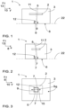
- Figure 1 illustrates schematically an electronic component according to a first embodiment in cross section shown from the direction of a side of the electronic component
- Figure 2 illustrates schematically the electronic component of Figure 1 in cross section shown from a direction of an end of the electronic component
- Figure 3 illustrates schematically an electronic component, such as the electronic component of Figures 1 and 2 , shown from a bottom of the electronic component
- Figure 4 illustrates schematically an electronic component according to a second embodiment in cross section shown from a direction of a side of the electronic component
- Figure 5 illustrates schematically the electronic component of Figure 4 in cross section shown from a direction of an end of the electronic component
- Figure 6 illustrates schematically an electronic component according to a third embodiment and a circuit board shown in cross section from a direction of a side of the electronic component
- Figure 7 illustrates schematically the electronic component and the circuit board of Figure 6 shown in cross section from a direction of an end of the electronic component
- Figure 8 illustrates schematically an electronic component,
- the parts have been simplified and the electronic components, for example, are mostly illustrated as rectangular blocks with straight edges extending parallel to the x-axis and the y-axis.
- the electronic component is then assumed to be oriented correctly when the four edges of the electronic component are parallel to the four edges of the surface, on which the electronic component is configured to be mounted to.
- the parts shown, such as the electronic component, the chip and circuit board could in reality have more complicated shapes than the figures of this disclosure illustrate.
- the chip may for example have the shape of a polygon with straight edges which form the sides of the chip.
- the general principles of alignment are, however, the same regardless of the shape of the electronic component, the circuit board and so on.
- the directional alignment of the electronic component is correct, possible orientation-sensitive axis/axes in the electronic component and the chip are oriented correctly with respect to a predetermined direction on the horizontal surface the electronic component is configured to be mounted to, such as the surface of the circuit board.
- the positional alignment of the component is correct, the location of every part of the component with respect to a predetermined point on the surface is correct.
- the alignment arrangements described in this disclosure are primarily focused on directional alignment.
- an output of the electronic component will accurately reflect the orientation of the circuit board in the apparatus, or a module 25 of the apparatus, to which it is mounted to.
- positional alignment may be important in some applications, and some embodiments described in this disclosure may also provide positional alignment.
- An electronic component 1, such as an electronic component according to one or more of Figures 1 - 11 is configured to be mounted on an external surface 21.
- the surface 21 being external refers to the surface 21 being a surface of a part separate from the electronic component 1.
- the electronic component 1 is designed to be provided on the surface 21 and to be attached to the surface 21.
- the surface 21 defines a plane 22, onto which the electronic component 1 is configured to be mounted.
- the electronic component 1 and the structural parts of the electronic component 1 are designed to have a predetermined alignment with respect to the plane 22.
- the electronic component 1 may also have a predetermined position with respect to the plane 22.
- the electronic component 1 may be mounted, directly or indirectly via fastening means, to the surface 21.
- the part of the electronic component 1 directed, or configured to be directed, when the electronic component 1 is mounted to the surface 21, towards the surface 21 is called bottom of the electronic component 1 in this disclosure, regardless of the actual direction of the electronic component 1 and the surface 21, when the electronic component 1 is mounted to an apparatus.
- the plane 22, namely the plane 22 defined by the surface 21, is illustrated as the xy-plane in this disclosure.
- This plane 22 can also be considered a horizontal plane in this disclosure.
- a vertical direction is indicated with a z-axis.
- the term “horizontal” refers in this disclosure to directions which are parallel to the xy-plane.
- terms such as “vertical”, “top”, “bottom”, “up”, “down”, “below” and “above” refer to the direction which is perpendicular to the xy-plane and to relative positions and distances in that direction. These terms do not indicate anything about how the component should be oriented with regard to the Earth's gravitational field when the component is manufactured, mounted, or when it is being used.
- an "end" of the electronic component 1 is an outer surface of the electronic component 1, which extends in a first direction 8, which is the direction of the x-axis, as seen in the figures, and in a third direction 13, which is the direction of the z-axis.
- the end of the electronic component 1 extends in a vertical direction from the surface 21, when the electronic component 1 is placed on the surface 21.
- the electronic component 1 may be considered to have two ends, which are opposite to each other in a horizontal direction.
- a "side" of the electronic component 1 is an outer surface of the electronic component 1, which extends in a second direction 10, which is the direction of the y-axis, as seen in the figures, and in the third direction 13, which is the direction of the z-axis.
- the side of the electronic component 1 extends in a vertical direction from the surface 21, when the electronic component 1 is placed on the surface 21.
- the electronic component 1 may be considered to have two sides, which are opposite to each other in a horizontal direction.
- a side of the electronic component 1 is considered to have a longer length in the horizontal direction than an end of the electronic component, if these dimensions are different from each other, but there is no functional difference between a side and an end, and these terms are used for explaining relative positions of features and references to figures only.
- the word "length" is used as a general term for a distance measure, or dimension, in the horizontal plane. Lengths can for example be measured in the direction of the x-axis, or in the direction of the y-axis, or in any other direction in the xy-plane.
- the ends and sides of the electronic component 1 are mostly illustrated as straight structures in the figures of this disclosure for clarity, whereby the corresponding lengths are linear measures.
- the shape of the electronic components 1 and their structural parts, such as the package 3 or a cap 14, may vary in actual applications, and at least some of the outer surfaces 6 of the electronic components 1 may be angled and/or curved.
- the electronic component 1 also has a top surface and a bottom surface, which extend in the direction of the plane 22, namely in the direction of the xy-plane, which is substantially horizontal when the electronic component 1 is placed on the surface 21, and which are provided opposite to each other in the vertical direction.
- the electronic component 1 comprises at least one electronic chip 2.
- the electronic chip 2 is housed within package 3.
- the package 3 provides protection for the chip(s) 2 inside the electronic component 1.
- the package 3 may be made of one material.
- the package 3 may comprise multiple materials, for instance some part(s) of the package 3 may be made of one material and some other part(s) of the package 3 from another material.
- the package 3, and thus the electronic component 1, may comprise a cap 14.
- the cap 14 may be made of a material different from the material of the rest of the package 3.
- the package 3 may comprise at least one of the following: a plastic material, a metal material, or a ceramic material.
- the cap 14 may comprise at least one of the following: a metal material or a ceramic material.
- the aligning structure(s) 5 are formed on an outer surface 6 of the electronic component 1.
- the aligning structure(s) 5 define at least two first aligning surface areas 7 in a first direction 8 and at least two second aligning surface areas 9 in a second direction 10.
- the first direction 8 and the second direction 10 are parallel to the plane 22 defined by the surface 21 and perpendicular in relation to each other.
- the first direction 8 is parallel to the x-axis and the second direction 10 is parallel to the y-axis, as defined in this disclosure.
- an aligning surface area such as a first aligning surface area 7, a second aligning surface area 9 or a further aligning surface area presented in this disclosure, may comprise a whole continuous surface area, such as a surface area limited by folds, corners and/or turns in the surface, or it may comprise a part of such a continuous surface area, in other words a partial surface area.
- an aligning structure 5 may comprise a hemispherical surface may comprise partial surface areas in the direction of x-axis, y-axis and y-axis, whereby it may form aligning surface areas in the first direction 8, the second direction 10 and also in a third direction 13 perpendicular to the first direction 8 and the second direction 10.
- the first aligning surface areas 7 may be provided on opposite sides of the aligning structure 5 in the first direction 8
- the second aligning surface areas 9 may be provided at opposite ends of the aligning structure 5, and so on.
- the first aligning surface areas 7 and the second aligning surface areas 9 are formed and spaced from each other in such a manner that at least a rotation of the electronic component 1 about an axis 11 perpendicular to the plane 22 defined by the surface 21 is prevented, when the first aligning surface areas 7 and the second aligning surface areas 9 are provided against counter surfaces 23 fixed on the surface 21 and conforming at least partly to the form of the respective aligning surface areas 7, 9.
- the first aligning surface areas 7 and the second aligning surface areas 9 have such a shape and mutual position that rotation about the axis 11 can be prevented by using the first aligning surface areas 7 and the second aligning surface areas 9 for the aligning.
- the first aligning surface areas 7 and the second aligning surface areas 9 may be used for aligning by providing the surface 21 with counter surfaces 23 conforming at least partly, preferably over the whole surface area designed to engage with the respective aligning surface area 7, 9, and positioning the counter surfaces 23 in such a manner that providing the electronic component on the surface 21 and bringing each one of the aligning surface areas 7, 9 and a corresponding counter surface 23 into contact with each other, the electronic component 1 is brought to a predetermined alignment with respect to the surface 21.
- the axis 11 may comprise an axis parallel with the y-axis, as defined in this disclosure.
- the axis 11 is perpendicular to the first direction 8 and the second direction 10.
- the first aligning surface areas 7 and the second aligning surface areas 9 are configured to have such a shape and mutual position that rotation about the axis 11 can be prevented by using the first aligning surface areas 7 and the second aligning surface areas 9 for the aligning in such a manner that the electronic component 1 has at least one aligning structure 5 and the shape of the aligning structure 5 is different from a body of revolution relative to the axis 11.
- the shape of the aligning structure 5, and thus the shape of the aligning surface areas 7, 9 may be used to align the electronic component 1 on the surface 21 and to prevent its rotation about the axis 11.
- the first aligning surface areas 7 and the second aligning surface areas 9 may be configured to have such a shape and mutual position that rotation about the axis 11 can be prevented by using the first aligning surface areas 7 and the second aligning surface areas 9 for the aligning in such a manner that the electronic component 1 has one or more aligning structures 5 having a shape of a body of revolution relative to the axis 11 and that the electronic component 1 has in total at least two aligning structures 5 spaced from each other.
- the position of the aligning structures 5, and thus the position of the aligning surface areas 7, 9 may be used to align the electronic component 1 on the surface 21 and to prevent rotation about the axis 11.
- the aligning surface areas 7, 9, 12 Spacing, in each direction, the aligning surface areas 7, 9, 12 from each other improves accuracy of alignment, as manufacturing tolerances have a smaller effect. More particularly, the further the aligning surface areas 7, 9, 12 are provided from each other, the better the accuracy of alignment. According to an embodiment, the second aligning surface areas 12 may be provided at opposite ends of the electronic component, such as shown in the Figures 8 and 9 .
- At least one aligning structure 5 is provided in a middle of the bottom of the electronic component 1, or at least in a middle area of the bottom of the electronic component 1.
- the aligning structure(s) 5 further define at least two third aligning surface areas 12 in the third direction 13.
- the third direction 13 is perpendicular to the first direction 8 and the second direction 10, as well as to the plane 22 defined by the surface 21, on which the electronic component 1 is configured to be mounted on.
- the third aligning surface areas 12 are configured to have such a shape and mutual position that the position of the electronic component 1 in the third direction 13 can be defined by the third aligning surface areas 12.
- the third aligning surface areas 12 are configured to have such a shape and mutual position that, together with the first aligning surface areas 7 and/or the second aligning surface areas 9, a rotation of the electronic component 1 about an axis parallel to the second direction 10, or the y-axis, and/or a rotation of the electronic component 1 about an axis parallel to the first direction 8, or the x-axis, respectively, can be prevented by using the first aligning surface areas 7 and third aligning surface areas 12 and/or the second aligning surface areas 9 and the third aligning surface areas 12, respectively.
- the third aligning surface areas 12 may be used for aligning the electronic component 1 on the surface 21 in a manner corresponding to that disclosed in connection with the first aligning surface areas 7 and the second aligning surface areas 9.
- the electronic component 1 comprises exactly one aligning structure 5.
- the electronic component 1 comprises exactly one aligning structure 5 and each one of the first aligning surface areas 7, the second aligning surface areas 9 and/or the third aligning surface areas 12 comprises a part of the outer surface 6 of the electronic component 1 in the area of the aligning structure 5.
- the first aligning surface areas 7, the second aligning surface areas 9 and/or the third aligning surface areas 12 are provided along the outer surface of the aligning structure 5.
- the aligning structure 5 comprises a shape different from a body of revolution about the axis 11 parallel with the third direction 13.
- the electronic component 1 comprises at least two aligning structures 5 and each one of the first aligning surface areas 7, the second aligning surface areas 9 and/or the third aligning surface areas 12 comprises in each case a part of the outer surface 6 of the electronic component in the area of one of the aligning structures 5.
- all the aligning surface areas 7, 9, 12 may be provided on a surface of a same aligning structure 5, at least one of the aligning surface areas 7, 9, 12 may be provided on a surface of another aligning structure 5, some of the aligning surface areas 7, 9, 12 may be provided on a surface of different aligning structures 5, or all aligning surface areas 7, 9, 12 may be provided on a surface of different aligning structures 5, depending on the embodiment.
- each aligning surface area 7, 9, 12 has a precise, predetermined three-dimensional shape.
- the aligning surface areas 7, 9, 12 form in each case a pair of aligning surface areas 7, 9, 12 in the respective direction 8, 10, 13 in such a manner that the electronic component 1 can be precisely aligned in each of the directions with respect to the surface 2, when the aligning surface areas 7, 9, 12 are provided against respective counter surfaces 23 fixed to the surface 21.
- Aligning the electronic component 1 precisely refers to aligning the electronic component 1 at an accuracy of at least 0.1 degrees at least in the first direction 8 and in the second direction 10, preferably in any direction.
- aligning the electronic component 1 precisely refers to aligning the electronic component 1 at an alignment inaccuracy of 0.1 degrees or less at least in the first direction 8 and in the second direction 10, preferably in any direction.
- At least one aligning structure 5 is formed as a protrusion protruding from the outer surface 6 or a recess extending from the outer surface 6 into the electronic component 1.
- the aligning structure 5 may protrude or recess with respect to outer surface 6 of the electronic component 1 the surrounding the aligning structure 5.
- the aligning structure 5 may also have both protruding and recessed portions.
- At least one aligning structure 5 is formed as a section of a cylinder, a section of a cone, a pyramid, a section of a pyramid, a cut pyramid, a section of a cut pyramid, a section of a sphere, an ellipsoid dome, a cube, a cuboid, a prism or a cut triangular prism.
- a part of at least one aligning structure may be formed as a section of a cylinder, a section of a cone, a pyramid, a section of a pyramid, a cut pyramid, a section of a cut pyramid, a section of a sphere, an ellipsoid dome, a cube, a cuboid, a prism or a cut triangular prism.
- at least one aligning structure 5 may have any two-dimensional or three-dimensional shape that enables, for its part, aligning the electronic component 1 on the surface 21, as disclosed in this disclosure.
- At least one of the first aligning surface areas 7, the second aligning surface areas 9 or the third aligning surface areas 12 has a three-dimensional shape.
- at least one of the aligning surface areas 7, 9, 12 may extend in all three dimensions.
- the aligning structure(s) 5 are provided in a part of the electronic component (1) made from a dimension accurate material.
- a dimension accurate material refers to a material that is dimension tolerant and dimensionally stable, at least dimension tolerant and dimensionally stable in normal manufacturing and use conditions.
- a position of the aligning structure 5, and especially the aligning surface areas 7, 9, 12, is known relative to the chip 2, preferably known with a measurement inaccuracy of 0.1 degrees or smaller.
- the aligning structure(s) 5 are provided in a part of the electronic component 1 made from metal, ceramic material or a plastic material.
- the metal material may comprise stainless steel, copper, or nickel-cobalt ferrous alloy, such as Kovar. Providing the aligning structure(s) 5 in such a part of the electronic component made from a dimension accurate material accuracy of the alignment electronic component can be significantly improved.
- the at least one chip 2 may be separated from the cap 14 by a gap and the cap 14 may be attached to a package base 17 to form an enclosure.
- the bottom surface of the cap 14 may be configured to be parallel to the plane of the circuit board, or a circuit board plane.
- the gap may comprise for instance an air gap.
- the cap may be formed from a metal, such as stainless steel, copper, or nickel-cobalt ferrous alloy, such as Kovar, and so on.
- the package base 17 may for instance be made of plastic.
- the package base 17 may be manufactured in a moulding process where the package base 17 is moulded around a leadframe, where a chip mounting element (not shown) and/or electronic leads 16 have been formed. Other methods can also be used to form a plastic package base 17.
- the package base 17 may alternatively be made of a ceramic material.
- the cap 14 can be attached to the package base 17 with glue or with any other method. The attachment region where the cap 14 is attached to the package base 17 may encircle the enclosure.
- the electronic chip 2 is orientation-sensitive.
- the electronic component 1, such as the chip 2 may comprise an axis of interest 15.
- the axis of interest 15 may be an orientation-sensitive axis.
- the chip 2 may comprise an axis of interest 15, the alignment of which in relation to the surface 21, to which the electronic component 1 is configured to be mounted, or an apparatus, where a module comprising the surface 21 is configured to be mounted to, is relevant for the purpose of the electronic component 1.
- the orientation-sensitive electronic chip 2 comprises the axis of interest 15, and the aligning surface areas 7, 9, 12 are configured to align at least the axis of interest 15 with respect to the surface 21.
- the axis of interest 15 may be associated with a function configured to be monitored using the electronic component 1.
- the electronic chip 2 comprises at least one of the following: an accelerometer configured to measure acceleration, a gyroscope configured to measure angular rotation, or a magnetometer.
- the accelerometer or gyroscope may be a MEMS accelerometer / gyroscope.
- the electronic chip 2 comprises another type of an orientation-sensitive chip.
- the one or more aligning structures 5 provided in the electronic component 1 define at least two aligning surface areas 7, 9, 12 in the direction of each one of the three dimensions in such a manner that they enable aligning the electronic component 1 to in all three dimensions with respect to the surface 21 comprising respective counter surfaces 23.
- the aligning structure(s) 5 may be configured to define the alignment of the electronic component 1 on the surface 21 in such a manner that rotation of the electronic component 1 about axes parallel to all three axes, namely parallel to the first direction 8, the second direction 10 and the third direction 13, is prevented.
- the aligning structure(s) 5 may be configured, in addition to preventing the rotation of the electronic component 1, to define the position of the electronic component 1 on the surface 21 in all three dimensions, namely in the first direction 8, the second direction 10 and the third direction 13.
- aligning the electronic component 1 on the surface 21 comprises aligning at least one predetermined axis of the electronic component 1, namely an axis of interest 15, in relation to a predetermined direction, such as the first direction 8, the second direction 10 and/or the third direction 13.
- aligning the electronic component 1 on the surface 21 comprises aligning the axis of interest 15 in relation to the first direction 8 or the second direction 10.
- aligning the electronic component 1 on the surface 21 comprises preventing rotation about an axis parallel to the third direction 13, which direction is also called the direction of the z-axis in this disclosure.
- aligning the electronic component 1 also aligns the chip 2 and the possible axis of interest 15, as long as the alignment of the chip 2 and the possible axis of interest 15, respectively, in relation to the electronic component 1 is also known.
- the ways of aligning the chip 2 and/or the axis of interest 15 in relation to the electronic component 1 are not in the scope of this disclosure.
- the package 3 may further comprise a plurality of electronic leads 16 protruding from the package 3.
- the leads 16 may be configured to extend from at least two sides of the package 3, preferably from at least two opposite sides of the package 3, as seen in Figures 4-5 and 10 - 11 , from a top part of the package 3 towards the surface 21 at least in the third direction 13.
- the electronic leads 16 may be configured to protrude from the package 3 at least in a direction corresponding to a downward direction.
- the electronic leads 16 may further be configured to extend outwards from the package 3, for instance in a bended manner, such as seen in Figures 4-5 and 10 - 11 .
- the electronic component may further comprise further external contacts and mounting elements which allow the component to be attached and electrically connected to the surface 21, such as a surface of a circuit board 20.
- Figure 9 illustrates schematically an electronic component according to a fourth embodiment, a circuit board and a module in cross section shown from the direction of a side of the electronic component
- Figure 10 illustrates schematically an electronic component according to a fifth embodiment in cross section and a circuit board shown from the direction of a side of the electronic component
- Figure 11 illustrates schematically an electronic component, such as the electronic component of Figure 10 , and a circuit board shown from above the electronic component.
- Figures 6 - 8 illustrate electronic components provided on circuit boards.
- a circuit board 20 may be configured to receive an electronic component 1 according to an embodiment or a combination of embodiments disclosed in this disclosure.
- the surface 21 of the circuit board 20 configured to receive the electronic component 1 comprises the surface 21, on to which the electronic component 1 is configured to be mounted to, and the surface 21 of the circuit board 20 defines the plane 22 referred to in connection with the embodiments of the electronic component 1.
- such a circuit board 20 comprises an electronic component 1 according to an embodiment or a combination of embodiments disclosed in this disclosure mounted on the surface 21 of the circuit board 20.
- the surface 21, which in this embodiment is thus the surface of the circuit board, is provided with at least one aligning counter structure 24.
- the aligning counter structure(s) 24 or parts of the aligning counter structure(s) 24 may comprise counter surfaces 23 conforming at least partly to the form of the respective aligning surface areas 7, 9 in the electronic component 1 for aligning the electronic component 1 on the circuit board 20.
- the counter surfaces 23 conform to the form of the respective aligning surface areas 7, 9 in the electronic component 1 over the whole surface area designed to engage with the respective aligning surface area 7, 9.
- the counter surfaces 23 are preferably positioned in such a manner that providing the electronic component 1 on the surface 21 and bringing each one of the aligning surface areas 7, 9 and a corresponding counter surface 23 into contact with each other, the electronic component 1 is brought to a predetermined alignment with respect to the surface 21 on the circuit board 20.
- the aligning structure 5 may be a part of the outer surface of the electronic component 1.
- at least one aligning structure 5 may comprise a predetermined part of the outer surface 6 of the electronic component 1 designed to enable alignment of the electronic component 1 on the surface 21.
- an aligning structure 5 and electronic component 1 may be similar to an embodiment or combination of embodiments disclosed in this disclosure.
- the circuit board 20 may be provided with aligning counter structure(s) 24, wherein the aligning counter structure(s) 24 or parts of the aligning counter structure(s) 24 comprise counter surfaces 23 conforming at least partly to the form of the respective aligning surface areas 7, 9 in such an aligning structure 5 in the electronic component 1, wherein the aligning structure 5 may be 1 designed to enable alignment of the electronic component 1 on the surface 21, when each one of the aligning surface areas 7, 9 is brought into contact with a corresponding counter surface 23.
- a part of at least one aligning structure 5 may be formed as a section of a cylinder, a section of a cone, a pyramid, a section of a pyramid, a cut pyramid, a section of a cut pyramid, a section of a sphere, an ellipsoid dome, a cube, a cuboid, a prism or a cut triangular prism, and the corresponding counter surface 23 of the respective aligning counter structure 24 conforms at least partly, and preferably over the whole surface area designed to engage with the respective aligning surface area 7, 9, to this shape. It is clear for a person skilled in the art that a surface and a counter surface conforming to each other refer to a recess in a surface conforming to a protrusion in a counter surface and vice versa.
- At least one aligning counter structure 24 may extend through the circuit board 20 in such a manner that the same counter structure 24 may also be used for aligning the circuit board 20 on an external module 25.
- the same aligning counter structure(s) 24 may be used to first align the electronic component 1 on the surface 21, such as on the circuit board 20, and later to align the surface 21, such as the circuit board 20, on a module 25.
- the module may comprise an apparatus or a part of an apparatus, wherein the electronic component 1 and the circuit board 20 are designed to be mounted to and, thus, used in for their actual purpose, such as for inertial measurements.
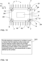
- Figure 12 illustrates schematically a method for aligning an electronic component.
- a method for aligning an electronic component 1, which may be an electronic component 1 according to an embodiment or combination of embodiments disclosed in this disclosure, on a surface 21 may comprise the step of providing 121 the electronic component 1 on the surface 21 in such a manner that the first aligning surface areas 7 and the second aligning surface areas 9 are provided against counter surfaces 23 fixed on the surface 21 for preventing at least a rotation of the electronic component 1 about an axis 11 perpendicular to the plane 22 defined by the surface 21.
- the method may further comprise calibrating the alignment of the electronic component 1 on the surface 21. More particularly, the same aligning structure(s) 5 used in assembling the electronic component 1 on the surface 21, such as to the circuit board 20, may be used for calibrating, for instance in a calibrator. This may improve the measurement accuracy further.
- the method may further comprise storing the calibration information in a memory (not shown) for later use. In such embodiments, the calibration made for the alignment of the electronic component 1 on the surface 21 may be used for calibrating the alignment of the component 1, and especially a possible axis of interest 15, with respect to the module 25 or apparatus comprising the module 25.
- This may enable more accurate aligning of the electronic component 1, and the axis of interest 15, with respect to a function to be monitored, and shorten the time needed for calibrating the alignment when the electronic component 1 mounted on the surface 21, for instance on the circuit board 20, is mounted to the module 25 or the apparatus.
- the function to be monitored may comprise for instance a measurement axis.
Landscapes
- Engineering & Computer Science (AREA)
- Microelectronics & Electronic Packaging (AREA)
- Physics & Mathematics (AREA)
- General Physics & Mathematics (AREA)
- Manufacturing & Machinery (AREA)
- Structures For Mounting Electric Components On Printed Circuit Boards (AREA)
Abstract
An electronic component (1) is configured to be mounted on an external surface (21), which surface (21) defines a plane (22). The electronic component (1) comprises at least one electronic chip (2) housed within package (3). The electronic component (1) is provided with one or more aligning structures (5), which aligning structure(s) (5) are formed on an outer surface (6) of the electronic component (1). The aligning structure(s) (5) define at least two first aligning surface areas (7) in a first direction (8) and at least two second aligning surface areas (9) in a second direction (10). The first aligning surface areas (7) and the second aligning surface areas (9) are formed and spaced from each other in such a manner that at least a rotation of the electronic component (1) about an axis (11) perpendicular to the plane (22) defined by the surface (21) is prevented, when the first aligning surface areas (7) and the second aligning surface areas (9) are provided against counter surfaces (23) fixed on the surface (21) and conforming at least partly to the form of the respective aligning surface areas (7, 9).
Description
- The present disclosure relates to electronic components, and particularly to electronic components where a die is protected by a surrounding package. The present disclosure further concerns the printed circuit board and a method for alignment of the package with a circuit board.
- Electronic dies, which may also be called chips, can be prepared by manufacturing electronic structures on a substrate and cutting the substrate into small pieces. The substrate may be a semiconductor substrate, for example a silicon substrate. Each die which is cut from the substrate may be placed inside a protective package by attaching it to a support structure and then building the package around it. The die can also be electrically connected to other chips inside the same package and/or to leads which extend to the outside of the package. The package and its contents can thereby form an electronic component which can be mounted on a circuit board. The circuit board can further be mounted on an apparatus, such as a vehicle, a machine or equipment or similar, depending on the application.
- Some dies are orientation-sensitive and have to be carefully aligned inside the package to ensure that the output of the electronic component is accurate. Orientation-sensitive dies include for instance magnetometer dies and dies which measure inertial variables such as acceleration or angular velocity.
- A problem related to such components is that the multi-phase mounting process includes many steps, which may cause inaccuracy in the direction of the die in relation to the circuit board and the apparatus. To compensate this, the alignment has to be calibrated in connection with the final phase mounting the circuit board to the apparatus, which takes time in the manufacturing process, and it is often necessary to rotate the circuit board with respect to the apparatus to align the die accurately with a direction of a desired measurement axis.
- An object of the present solution is to provide a new electronic component, a new circuit board and a new method for aligning an electronic component on the circuit board.
- The object of the disclosure is achieved by an electronic component, a circuit board, and a method, which are characterized by what is stated in the independent claims. Some embodiments of the disclosure are disclosed in the dependent claims.
- The disclosure is based on the idea of forming parts of an outer surface of the electronic component to enable accurate aligning of especially an axis of interest of a chip provided in the electronic component with a surface, on which the electronic component is designed to be provided on, such as the circuit board.
- An advantage of the method and apparatus is that accuracy of the alignment between the axis of interest and the surface, on which the electronic component is provided on, can be significantly improved.
- In the following the disclosure will be described in greater detail by means of preferred embodiments with reference to the accompanying drawings, in which
-
Figure 1 illustrates schematically an electronic component according to a first embodiment in cross section shown from the direction of a side of the electronic component; -
Figure 2 illustrates schematically the electronic component ofFigure 1 in cross section shown from a direction of an end of the electronic component; -
Figure 3 illustrates schematically an electronic component, such as the electronic component ofFigures 1 and 2 , shown from a bottom of the electronic component; -
Figure 4 illustrates schematically an electronic component according to a second embodiment in cross section shown from a direction of a side of the electronic component; -
Figure 5 illustrates schematically the electronic component ofFigure 4 in cross section shown from a direction of an end of the electronic component; -
Figure 6 illustrates schematically an electronic component according to a third embodiment and a circuit board shown in cross section from a direction of a side of the electronic component; -
Figure 7 illustrates schematically the electronic component and the circuit board ofFigure 6 shown in cross section from a direction of an end of the electronic component; -
Figure 8 illustrates schematically an electronic component, such as the electronic component ofFigures 6 and7 , and a circuit board shown from above the electronic component; -
Figure 9 illustrates schematically an electronic component according to a fourth embodiment, a circuit board and a module in cross section shown from the direction of a side of the electronic component; -
Figure 10 illustrates schematically an electronic component according to a fifth embodiment in cross section and a circuit board shown from the direction of a side of the electronic component; -
Figure 11 illustrates schematically an electronic component, such as the electronic component ofFigure 10 , and a circuit board shown from above the electronic component; and -
Figure 12 illustrates schematically a method for aligning an electronic component. - The figures are provided for schematically illustrating features of the solution only. The figures do not show all the features of the objects and are not shown to scale.
- The description relates to electronic components, and particularly to electronic components where a die, also called a chip, is protected by a surrounding package. The description further concerns the printed circuit board and a method for alignment of the package with a circuit board, also called a printed circuit board (PCB).
-
Figures 1 - 11 disclose some embodiments ofelectronic components 1. For example,Figure 1 illustrates schematically an electronic component according to a first embodiment in cross section shown from the direction of a side of the electronic component;Figure 2 illustrates schematically the electronic component ofFigure 1 in cross section shown from a direction of an end of the electronic component;Figure 3 illustrates schematically an electronic component, such as the electronic component ofFigures 1 and 2 , shown from a bottom of the electronic component;Figure 4 illustrates schematically an electronic component according to a second embodiment in cross section shown from a direction of a side of the electronic component;Figure 5 illustrates schematically the electronic component ofFigure 4 in cross section shown from a direction of an end of the electronic component;Figure 6 illustrates schematically an electronic component according to a third embodiment and a circuit board shown in cross section from a direction of a side of the electronic component;Figure 7 illustrates schematically the electronic component and the circuit board ofFigure 6 shown in cross section from a direction of an end of the electronic component; andFigure 8 illustrates schematically an electronic component, such as the electronic component ofFigures 6 and7 , and a circuit board shown from above the electronic component. - For the sake of clarity, in the figures of this disclosure, shapes of the parts have been simplified and the electronic components, for example, are mostly illustrated as rectangular blocks with straight edges extending parallel to the x-axis and the y-axis. The electronic component is then assumed to be oriented correctly when the four edges of the electronic component are parallel to the four edges of the surface, on which the electronic component is configured to be mounted to. However, the parts shown, such as the electronic component, the chip and circuit board could in reality have more complicated shapes than the figures of this disclosure illustrate. The chip may for example have the shape of a polygon with straight edges which form the sides of the chip.
- The general principles of alignment are, however, the same regardless of the shape of the electronic component, the circuit board and so on. When the directional alignment of the electronic component is correct, possible orientation-sensitive axis/axes in the electronic component and the chip are oriented correctly with respect to a predetermined direction on the horizontal surface the electronic component is configured to be mounted to, such as the surface of the circuit board. Similarly, when the positional alignment of the component is correct, the location of every part of the component with respect to a predetermined point on the surface is correct. As described in more detail below, the alignment arrangements described in this disclosure are primarily focused on directional alignment. When the directional alignment of the electronic component comprising an orientation-sensitive chip is correct, an output of the electronic component will accurately reflect the orientation of the circuit board in the apparatus, or a
module 25 of the apparatus, to which it is mounted to. Also positional alignment may be important in some applications, and some embodiments described in this disclosure may also provide positional alignment. - An
electronic component 1, such as an electronic component according to one or more ofFigures 1 - 11 , is configured to be mounted on anexternal surface 21. Thesurface 21 being external refers to thesurface 21 being a surface of a part separate from theelectronic component 1. In other words, theelectronic component 1 is designed to be provided on thesurface 21 and to be attached to thesurface 21. - The
surface 21 defines aplane 22, onto which theelectronic component 1 is configured to be mounted. In other words, theelectronic component 1 and the structural parts of theelectronic component 1 are designed to have a predetermined alignment with respect to theplane 22. Theelectronic component 1 may also have a predetermined position with respect to theplane 22. Theelectronic component 1 may be mounted, directly or indirectly via fastening means, to thesurface 21. - The part of the
electronic component 1 directed, or configured to be directed, when theelectronic component 1 is mounted to thesurface 21, towards thesurface 21 is called bottom of theelectronic component 1 in this disclosure, regardless of the actual direction of theelectronic component 1 and thesurface 21, when theelectronic component 1 is mounted to an apparatus. - The
plane 22, namely theplane 22 defined by thesurface 21, is illustrated as the xy-plane in this disclosure. Thisplane 22 can also be considered a horizontal plane in this disclosure. Similarly, a vertical direction is indicated with a z-axis. The term "horizontal" refers in this disclosure to directions which are parallel to the xy-plane. In this disclosure, terms such as "vertical", "top", "bottom", "up", "down", "below" and "above" refer to the direction which is perpendicular to the xy-plane and to relative positions and distances in that direction. These terms do not indicate anything about how the component should be oriented with regard to the Earth's gravitational field when the component is manufactured, mounted, or when it is being used. - In this disclosure, an "end" of the
electronic component 1 is an outer surface of theelectronic component 1, which extends in afirst direction 8, which is the direction of the x-axis, as seen in the figures, and in athird direction 13, which is the direction of the z-axis. In other words, the end of theelectronic component 1 extends in a vertical direction from thesurface 21, when theelectronic component 1 is placed on thesurface 21. Theelectronic component 1 may be considered to have two ends, which are opposite to each other in a horizontal direction. - In this disclosure, a "side" of the
electronic component 1 is an outer surface of theelectronic component 1, which extends in asecond direction 10, which is the direction of the y-axis, as seen in the figures, and in thethird direction 13, which is the direction of the z-axis. In other words, the side of theelectronic component 1 extends in a vertical direction from thesurface 21, when theelectronic component 1 is placed on thesurface 21. Theelectronic component 1 may be considered to have two sides, which are opposite to each other in a horizontal direction. In this disclosure, a side of theelectronic component 1 is considered to have a longer length in the horizontal direction than an end of the electronic component, if these dimensions are different from each other, but there is no functional difference between a side and an end, and these terms are used for explaining relative positions of features and references to figures only. - In this disclosure, the word "length" is used as a general term for a distance measure, or dimension, in the horizontal plane. Lengths can for example be measured in the direction of the x-axis, or in the direction of the y-axis, or in any other direction in the xy-plane. The ends and sides of the
electronic component 1 are mostly illustrated as straight structures in the figures of this disclosure for clarity, whereby the corresponding lengths are linear measures. However, the shape of theelectronic components 1 and their structural parts, such as thepackage 3 or acap 14, may vary in actual applications, and at least some of theouter surfaces 6 of theelectronic components 1 may be angled and/or curved. - The
electronic component 1 also has a top surface and a bottom surface, which extend in the direction of theplane 22, namely in the direction of the xy-plane, which is substantially horizontal when theelectronic component 1 is placed on thesurface 21, and which are provided opposite to each other in the vertical direction. - The
electronic component 1 comprises at least oneelectronic chip 2. In theelectronic component 1, theelectronic chip 2 is housed withinpackage 3. Thepackage 3 provides protection for the chip(s) 2 inside theelectronic component 1. According to an embodiment, thepackage 3 may be made of one material. According to another embodiment, thepackage 3 may comprise multiple materials, for instance some part(s) of thepackage 3 may be made of one material and some other part(s) of thepackage 3 from another material. According to an embodiment, thepackage 3, and thus theelectronic component 1, may comprise acap 14. Thecap 14 may be made of a material different from the material of the rest of thepackage 3. According to an embodiment, thepackage 3 may comprise at least one of the following: a plastic material, a metal material, or a ceramic material. According to an embodiment, thecap 14 may comprise at least one of the following: a metal material or a ceramic material. - The
electronic component 1, such as an electronic component according to one or more ofFigures 1 - 11 , is provided with one or more aligningstructures 5. The aligning structure(s) 5 are formed on anouter surface 6 of theelectronic component 1. The aligning structure(s) 5 define at least two first aligningsurface areas 7 in afirst direction 8 and at least two second aligningsurface areas 9 in asecond direction 10. Thefirst direction 8 and thesecond direction 10 are parallel to theplane 22 defined by thesurface 21 and perpendicular in relation to each other. According to an embodiment, thefirst direction 8 is parallel to the x-axis and thesecond direction 10 is parallel to the y-axis, as defined in this disclosure. - In this disclosure, an aligning surface area, such as a first aligning
surface area 7, a second aligningsurface area 9 or a further aligning surface area presented in this disclosure, may comprise a whole continuous surface area, such as a surface area limited by folds, corners and/or turns in the surface, or it may comprise a part of such a continuous surface area, in other words a partial surface area. For instance, according to an embodiment, an aligningstructure 5 may comprise a hemispherical surface may comprise partial surface areas in the direction of x-axis, y-axis and y-axis, whereby it may form aligning surface areas in thefirst direction 8, thesecond direction 10 and also in athird direction 13 perpendicular to thefirst direction 8 and thesecond direction 10. Thus, the first aligningsurface areas 7 may be provided on opposite sides of the aligningstructure 5 in thefirst direction 8, the second aligningsurface areas 9 may be provided at opposite ends of the aligningstructure 5, and so on. - In the
electronic component 1, such as anelectronic component 1 according to one or more ofFigures 1 - 11 , the first aligningsurface areas 7 and the second aligningsurface areas 9 are formed and spaced from each other in such a manner that at least a rotation of theelectronic component 1 about anaxis 11 perpendicular to theplane 22 defined by thesurface 21 is prevented, when the first aligningsurface areas 7 and the second aligningsurface areas 9 are provided against counter surfaces 23 fixed on thesurface 21 and conforming at least partly to the form of the respective aligningsurface areas surface areas 7 and the second aligningsurface areas 9 have such a shape and mutual position that rotation about theaxis 11 can be prevented by using the first aligningsurface areas 7 and the second aligningsurface areas 9 for the aligning. The first aligningsurface areas 7 and the second aligningsurface areas 9 may be used for aligning by providing thesurface 21 withcounter surfaces 23 conforming at least partly, preferably over the whole surface area designed to engage with the respective aligningsurface area surface 21 and bringing each one of the aligningsurface areas corresponding counter surface 23 into contact with each other, theelectronic component 1 is brought to a predetermined alignment with respect to thesurface 21. - The
axis 11 may comprise an axis parallel with the y-axis, as defined in this disclosure. Theaxis 11 is perpendicular to thefirst direction 8 and thesecond direction 10. - According to an embodiment, the first aligning
surface areas 7 and the second aligningsurface areas 9 are configured to have such a shape and mutual position that rotation about theaxis 11 can be prevented by using the first aligningsurface areas 7 and the second aligningsurface areas 9 for the aligning in such a manner that theelectronic component 1 has at least one aligningstructure 5 and the shape of the aligningstructure 5 is different from a body of revolution relative to theaxis 11. Thereby, the shape of the aligningstructure 5, and thus the shape of the aligningsurface areas electronic component 1 on thesurface 21 and to prevent its rotation about theaxis 11. According to another embodiment, the first aligningsurface areas 7 and the second aligningsurface areas 9 may be configured to have such a shape and mutual position that rotation about theaxis 11 can be prevented by using the first aligningsurface areas 7 and the second aligningsurface areas 9 for the aligning in such a manner that theelectronic component 1 has one or more aligningstructures 5 having a shape of a body of revolution relative to theaxis 11 and that theelectronic component 1 has in total at least two aligningstructures 5 spaced from each other. Thereby, the position of the aligningstructures 5, and thus the position of the aligningsurface areas electronic component 1 on thesurface 21 and to prevent rotation about theaxis 11. Spacing, in each direction, the aligningsurface areas surface areas surface areas 12 may be provided at opposite ends of the electronic component, such as shown in theFigures 8 and9 . - According to an embodiment, at least one aligning
structure 5 is provided in a middle of the bottom of theelectronic component 1, or at least in a middle area of the bottom of theelectronic component 1. - According to an embodiment, the aligning structure(s) 5 further define at least two third aligning
surface areas 12 in thethird direction 13. As described above, thethird direction 13 is perpendicular to thefirst direction 8 and thesecond direction 10, as well as to theplane 22 defined by thesurface 21, on which theelectronic component 1 is configured to be mounted on. According to an embodiment, the third aligningsurface areas 12 are configured to have such a shape and mutual position that the position of theelectronic component 1 in thethird direction 13 can be defined by the third aligningsurface areas 12. According to an embodiment, the third aligningsurface areas 12 are configured to have such a shape and mutual position that, together with the first aligningsurface areas 7 and/or the second aligningsurface areas 9, a rotation of theelectronic component 1 about an axis parallel to thesecond direction 10, or the y-axis, and/or a rotation of theelectronic component 1 about an axis parallel to thefirst direction 8, or the x-axis, respectively, can be prevented by using the first aligningsurface areas 7 and third aligningsurface areas 12 and/or the second aligningsurface areas 9 and the third aligningsurface areas 12, respectively. The third aligningsurface areas 12 may be used for aligning theelectronic component 1 on thesurface 21 in a manner corresponding to that disclosed in connection with the first aligningsurface areas 7 and the second aligningsurface areas 9. - According to an embodiment, the
electronic component 1 comprises exactly one aligningstructure 5. According to an embodiment, theelectronic component 1 comprises exactly one aligningstructure 5 and each one of the first aligningsurface areas 7, the second aligningsurface areas 9 and/or the third aligningsurface areas 12 comprises a part of theouter surface 6 of theelectronic component 1 in the area of the aligningstructure 5. In other words, the first aligningsurface areas 7, the second aligningsurface areas 9 and/or the third aligningsurface areas 12 are provided along the outer surface of the aligningstructure 5. In such embodiments, as described above, the aligningstructure 5 comprises a shape different from a body of revolution about theaxis 11 parallel with thethird direction 13. - According to an embodiment, the
electronic component 1 comprises at least two aligningstructures 5 and each one of the first aligningsurface areas 7, the second aligningsurface areas 9 and/or the third aligningsurface areas 12 comprises in each case a part of theouter surface 6 of the electronic component in the area of one of the aligningstructures 5. In other words, all the aligningsurface areas structure 5, at least one of the aligningsurface areas structure 5, some of the aligningsurface areas structures 5, or all aligningsurface areas structures 5, depending on the embodiment. - According to an embodiment, each aligning
surface area surface areas surface areas respective direction electronic component 1 can be precisely aligned in each of the directions with respect to thesurface 2, when the aligningsurface areas surface 21. Aligning theelectronic component 1 precisely refers to aligning theelectronic component 1 at an accuracy of at least 0.1 degrees at least in thefirst direction 8 and in thesecond direction 10, preferably in any direction. In other words, aligning theelectronic component 1 precisely refers to aligning theelectronic component 1 at an alignment inaccuracy of 0.1 degrees or less at least in thefirst direction 8 and in thesecond direction 10, preferably in any direction. - According to an embodiment, at least one aligning
structure 5 is formed as a protrusion protruding from theouter surface 6 or a recess extending from theouter surface 6 into theelectronic component 1. Depending on the embodiment, the aligningstructure 5 may protrude or recess with respect toouter surface 6 of theelectronic component 1 the surrounding the aligningstructure 5. According to an embodiment, the aligningstructure 5 may also have both protruding and recessed portions. - According to an embodiment, at least one aligning
structure 5 is formed as a section of a cylinder, a section of a cone, a pyramid, a section of a pyramid, a cut pyramid, a section of a cut pyramid, a section of a sphere, an ellipsoid dome, a cube, a cuboid, a prism or a cut triangular prism. According to an embodiment, a part of at least one aligning structure may be formed as a section of a cylinder, a section of a cone, a pyramid, a section of a pyramid, a cut pyramid, a section of a cut pyramid, a section of a sphere, an ellipsoid dome, a cube, a cuboid, a prism or a cut triangular prism. According to a further embodiment, at least one aligningstructure 5 may have any two-dimensional or three-dimensional shape that enables, for its part, aligning theelectronic component 1 on thesurface 21, as disclosed in this disclosure. - According to an embodiment, at least one of the first aligning
surface areas 7, the second aligningsurface areas 9 or the third aligningsurface areas 12 has a three-dimensional shape. In other words, at least one of the aligningsurface areas - According to an embodiment, the aligning structure(s) 5 are provided in a part of the electronic component (1) made from a dimension accurate material. A dimension accurate material refers to a material that is dimension tolerant and dimensionally stable, at least dimension tolerant and dimensionally stable in normal manufacturing and use conditions. Thereby, a position of the aligning
structure 5, and especially the aligningsurface areas chip 2, preferably known with a measurement inaccuracy of 0.1 degrees or smaller. According to an embodiment, the aligning structure(s) 5 are provided in a part of theelectronic component 1 made from metal, ceramic material or a plastic material. According to an embodiment, the metal material may comprise stainless steel, copper, or nickel-cobalt ferrous alloy, such as Kovar. Providing the aligning structure(s) 5 in such a part of the electronic component made from a dimension accurate material accuracy of the alignment electronic component can be significantly improved. - According to an embodiment, the
electronic component 1 further comprises acap 14.Such caps 14 are known in the art and thecap 14 may cover for instance a top or a bottom of thepackage 3 and, thus, theelectronic component 1. According to such an embodiment, at least one of the aligningstructures 5 may be provided in thecap 14. - According to an embodiment, the at least one
chip 2 may be separated from thecap 14 by a gap and thecap 14 may be attached to apackage base 17 to form an enclosure. According to an embodiment, the bottom surface of thecap 14 may be configured to be parallel to the plane of the circuit board, or a circuit board plane. The gap may comprise for instance an air gap. - According to an embodiment, the cap may be formed from a metal, such as stainless steel, copper, or nickel-cobalt ferrous alloy, such as Kovar, and so on.
- According to an embodiment, the
package base 17 may for instance be made of plastic. According to an embodiment, thepackage base 17 may be manufactured in a moulding process where thepackage base 17 is moulded around a leadframe, where a chip mounting element (not shown) and/orelectronic leads 16 have been formed. Other methods can also be used to form aplastic package base 17. Thepackage base 17 may alternatively be made of a ceramic material. Thecap 14 can be attached to thepackage base 17 with glue or with any other method. The attachment region where thecap 14 is attached to thepackage base 17 may encircle the enclosure. - According to an embodiment, the
electronic chip 2 is orientation-sensitive. According to an embodiment, theelectronic component 1, such as thechip 2, may comprise an axis ofinterest 15. The axis ofinterest 15 may be an orientation-sensitive axis. In other words, thechip 2 may comprise an axis ofinterest 15, the alignment of which in relation to thesurface 21, to which theelectronic component 1 is configured to be mounted, or an apparatus, where a module comprising thesurface 21 is configured to be mounted to, is relevant for the purpose of theelectronic component 1. According to an embodiment, the orientation-sensitiveelectronic chip 2 comprises the axis ofinterest 15, and the aligningsurface areas interest 15 with respect to thesurface 21. According to an embodiment, the axis ofinterest 15 may be associated with a function configured to be monitored using theelectronic component 1. - According to an embodiment, the
electronic chip 2 comprises at least one of the following: an accelerometer configured to measure acceleration, a gyroscope configured to measure angular rotation, or a magnetometer. The accelerometer or gyroscope may be a MEMS accelerometer / gyroscope. According to an embodiment, theelectronic chip 2 comprises another type of an orientation-sensitive chip. - According to an embodiment, the one or more aligning
structures 5 provided in theelectronic component 1 define at least two aligningsurface areas electronic component 1 to in all three dimensions with respect to thesurface 21 comprising respective counter surfaces 23. According to an embodiment, the aligning structure(s) 5 may be configured to define the alignment of theelectronic component 1 on thesurface 21 in such a manner that rotation of theelectronic component 1 about axes parallel to all three axes, namely parallel to thefirst direction 8, thesecond direction 10 and thethird direction 13, is prevented. According to an embodiment, the aligning structure(s) 5 may be configured, in addition to preventing the rotation of theelectronic component 1, to define the position of theelectronic component 1 on thesurface 21 in all three dimensions, namely in thefirst direction 8, thesecond direction 10 and thethird direction 13. - According to an embodiment, aligning the
electronic component 1 on thesurface 21 comprises aligning at least one predetermined axis of theelectronic component 1, namely an axis ofinterest 15, in relation to a predetermined direction, such as thefirst direction 8, thesecond direction 10 and/or thethird direction 13. According to an embodiment, aligning theelectronic component 1 on thesurface 21 comprises aligning the axis ofinterest 15 in relation to thefirst direction 8 or thesecond direction 10. According to an embodiment, aligning theelectronic component 1 on thesurface 21 comprises preventing rotation about an axis parallel to thethird direction 13, which direction is also called the direction of the z-axis in this disclosure. - It is clear for a person skilled in the art that aligning the
electronic component 1, as disclosed in this disclosure, also aligns thechip 2 and the possible axis ofinterest 15, as long as the alignment of thechip 2 and the possible axis ofinterest 15, respectively, in relation to theelectronic component 1 is also known. The ways of aligning thechip 2 and/or the axis ofinterest 15 in relation to theelectronic component 1 are not in the scope of this disclosure. - According to an embodiment, the
package 3 may further comprise a plurality ofelectronic leads 16 protruding from thepackage 3. The leads 16 may be configured to extend from at least two sides of thepackage 3, preferably from at least two opposite sides of thepackage 3, as seen inFigures 4-5 and10 - 11 , from a top part of thepackage 3 towards thesurface 21 at least in thethird direction 13. In other words, the electronic leads 16 may be configured to protrude from thepackage 3 at least in a direction corresponding to a downward direction. According to an embodiment, the electronic leads 16 may further be configured to extend outwards from thepackage 3, for instance in a bended manner, such as seen inFigures 4-5 and10 - 11 . - The electronic component may further comprise further external contacts and mounting elements which allow the component to be attached and electrically connected to the
surface 21, such as a surface of acircuit board 20. -
Figure 9 illustrates schematically an electronic component according to a fourth embodiment, a circuit board and a module in cross section shown from the direction of a side of the electronic component;Figure 10 illustrates schematically an electronic component according to a fifth embodiment in cross section and a circuit board shown from the direction of a side of the electronic component; andFigure 11 illustrates schematically an electronic component, such as the electronic component ofFigure 10 , and a circuit board shown from above the electronic component. AlsoFigures 6 - 8 illustrate electronic components provided on circuit boards. - According to an embodiment, a
circuit board 20 may be configured to receive anelectronic component 1 according to an embodiment or a combination of embodiments disclosed in this disclosure. According to an embodiment, thesurface 21 of thecircuit board 20 configured to receive theelectronic component 1 comprises thesurface 21, on to which theelectronic component 1 is configured to be mounted to, and thesurface 21 of thecircuit board 20 defines theplane 22 referred to in connection with the embodiments of theelectronic component 1. According to an embodiment, such acircuit board 20 comprises anelectronic component 1 according to an embodiment or a combination of embodiments disclosed in this disclosure mounted on thesurface 21 of thecircuit board 20. - According to an embodiment, the
surface 21, which in this embodiment is thus the surface of the circuit board, is provided with at least one aligningcounter structure 24. The aligning counter structure(s) 24 or parts of the aligning counter structure(s) 24 may comprise counter surfaces 23 conforming at least partly to the form of the respective aligningsurface areas electronic component 1 for aligning theelectronic component 1 on thecircuit board 20. According to an embodiment, the counter surfaces 23 conform to the form of the respective aligningsurface areas electronic component 1 over the whole surface area designed to engage with the respective aligningsurface area electronic component 1 on thesurface 21 and bringing each one of the aligningsurface areas corresponding counter surface 23 into contact with each other, theelectronic component 1 is brought to a predetermined alignment with respect to thesurface 21 on thecircuit board 20. - According to an embodiment, such as an embodiment of
Figures 10 and11 , the aligningstructure 5 may be a part of the outer surface of theelectronic component 1. In other words, rather than an aligningstructure 5 provided in theelectronic component 1 specifically for the purpose of aligning the electronic component with respect to thesurface 21, such as a recess or a protrusion, at least one aligningstructure 5 may comprise a predetermined part of theouter surface 6 of theelectronic component 1 designed to enable alignment of theelectronic component 1 on thesurface 21. Otherwise, such an aligningstructure 5 andelectronic component 1 may be similar to an embodiment or combination of embodiments disclosed in this disclosure. According to an embodiment, thecircuit board 20 may be provided with aligning counter structure(s) 24, wherein the aligning counter structure(s) 24 or parts of the aligning counter structure(s) 24 comprise counter surfaces 23 conforming at least partly to the form of the respective aligningsurface areas structure 5 in theelectronic component 1, wherein the aligningstructure 5 may be 1 designed to enable alignment of theelectronic component 1 on thesurface 21, when each one of the aligningsurface areas corresponding counter surface 23. - According to an embodiment, a part of at least one aligning
structure 5 may be formed as a section of a cylinder, a section of a cone, a pyramid, a section of a pyramid, a cut pyramid, a section of a cut pyramid, a section of a sphere, an ellipsoid dome, a cube, a cuboid, a prism or a cut triangular prism, and thecorresponding counter surface 23 of the respective aligningcounter structure 24 conforms at least partly, and preferably over the whole surface area designed to engage with the respective aligningsurface area - According to an embodiment, such as the embodiment of
Figure 9 , at least one aligningcounter structure 24 may extend through thecircuit board 20 in such a manner that thesame counter structure 24 may also be used for aligning thecircuit board 20 on anexternal module 25. In other words, the same aligning counter structure(s) 24 may be used to first align theelectronic component 1 on thesurface 21, such as on thecircuit board 20, and later to align thesurface 21, such as thecircuit board 20, on amodule 25. The module may comprise an apparatus or a part of an apparatus, wherein theelectronic component 1 and thecircuit board 20 are designed to be mounted to and, thus, used in for their actual purpose, such as for inertial measurements. -
Figure 12 illustrates schematically a method for aligning an electronic component. - According to a method, such as the method of
Figure 12 , for aligning anelectronic component 1, which may be anelectronic component 1 according to an embodiment or combination of embodiments disclosed in this disclosure, on asurface 21 may comprise the step of providing 121 theelectronic component 1 on thesurface 21 in such a manner that the first aligningsurface areas 7 and the second aligningsurface areas 9 are provided against counter surfaces 23 fixed on thesurface 21 for preventing at least a rotation of theelectronic component 1 about anaxis 11 perpendicular to theplane 22 defined by thesurface 21. - According to an embodiment, the method may further comprise calibrating the alignment of the
electronic component 1 on thesurface 21. More particularly, the same aligning structure(s) 5 used in assembling theelectronic component 1 on thesurface 21, such as to thecircuit board 20, may be used for calibrating, for instance in a calibrator. This may improve the measurement accuracy further. According to a further embodiment, the method may further comprise storing the calibration information in a memory (not shown) for later use. In such embodiments, the calibration made for the alignment of theelectronic component 1 on thesurface 21 may be used for calibrating the alignment of thecomponent 1, and especially a possible axis ofinterest 15, with respect to themodule 25 or apparatus comprising themodule 25. This may enable more accurate aligning of theelectronic component 1, and the axis ofinterest 15, with respect to a function to be monitored, and shorten the time needed for calibrating the alignment when theelectronic component 1 mounted on thesurface 21, for instance on thecircuit board 20, is mounted to themodule 25 or the apparatus. The function to be monitored may comprise for instance a measurement axis. Better accuracy of aligning the axis ofinterest 15 in theelectronic component 1, for instance of thechip 2, with the intended measurement axis of themodule 25 or the apparatus improves the actual measurement accuracy in the apparatus and enables improved quality of the apparatus, such as a more accurate control of the apparatus.
Claims (21)
- An electronic component configured to be mounted on an external surface, which surface defines a plane,the electronic component comprisingat least one electronic chip housed within package,characterized in thatthe electronic component is provided with one or more aligning structures, which aligning structure(s) are formed on an outer surface of the electronic component, wherein the aligning structure(s) define at least two first aligning surface areas in a first direction and at least two second aligning surface areas in a second direction, wherein the first direction and the second direction are parallel to said plane defined by the surface and perpendicular in relation to each other,and wherein the first aligning surface areas and the second aligning surface areas are formed and spaced from each other in such a manner that at least a rotation of the electronic component about an axis perpendicular to the plane defined by the surface is prevented, when the first aligning surface areas and the second aligning surface areas are provided against counter surfaces fixed on the surface and conforming at least partly to the form of the respective aligning surface areas.
- An electronic component according to claim 1, wherein the aligning structure(s) further define at least two third aligning surface areas in a third direction,
wherein third direction is perpendicular to the first direction and the second direction, as well as to said plane defined by the surface. - An electronic component according to claim 1 or 2, wherein the electronic component comprises exactly one aligning structure and wherein each one of the first aligning surface areas, the second aligning surface areas and/or the third aligning surface areas comprises a part of the outer surface of the electronic component in the area of the aligning structure.
- An electronic component according to claim 1 or 2, wherein the electronic component comprises at least two aligning structures and wherein each one of the first aligning surface areas, the second aligning surface areas and/or the third aligning surface areas comprises in each case a part of the outer surface of one of the aligning structures.
- An electronic component according to any one of claims 1 - 4, wherein the aligning structure(s) are provided in a part of the electronic component made from a dimension accurate material.
- An electronic component according to claim 5, wherein the aligning structure(s) are provided in a part of the electronic component made from metal, ceramic material, or plastic material.
- An electronic component according to any one of claims 1 - 6, wherein each aligning surface area has a precise, predetermined three-dimensional shape,
whereby the aligning surface areas form in each case a pair of aligning surface areas in the respective direction in such a manner that the electronic component can be precisely aligned in each of the directions with respect to the surface, when the aligning surface areas are provided against respective counter surfaces fixed to the surface. - An electronic component according to claim 7, wherein aligning the electronic component precisely comprises aligning the electronic component at an alignment inaccuracy of 0.1 degrees or less at least in the first direction and in the second direction.
- An electronic component according to any one of claims 1 - 8, wherein at least one aligning structure is formed as a protrusion protruding from the outer surface or a recess extending from the outer surface into the electronic component.
- An electronic component according to any one of claims 1 - 9, wherein at least one aligning structure is formed as a section of a cylinder, a section of a cone, a pyramid, a section of a pyramid, a cut pyramid, a section of a cut pyramid, a section of a sphere, an ellipsoid dome, a cube, a cuboid, a prism, or a cut triangular prism.
- An electronic component according to any one of claims 1 - 10, wherein the electronic component comprises a cap and wherein at least one of the aligning structures is provided in the cap.
- An electronic component according to any one of claims 1 - 11, wherein at least one of the first aligning surface areas, the second aligning surface areas or the third aligning surface areas has a three-dimensional shape.
- An electronic component according to any one of claims 1 - 12, wherein the electronic chip is orientation-sensitive.
- An electronic component according to claim 13, wherein the orientation-sensitive electronic chip comprises an axis of interest, and wherein the aligning surface areas are configured to align at least the axis of interest with respect to the surface.
- An electronic component according to claim 13 or 14, wherein the electronic chip comprises at least one of the following: an accelerometer configured to measure acceleration, a gyroscope configured to measure angular rotation, or a magnetometer.
- An electronic component according to any one of claims 1 - 15, wherein
the one or more aligning structures provided in the electronic component define at least two aligning surface areas in the direction of each one of the three dimensions in such a manner that they enable aligning the electronic component to in all three dimensions with respect to the surface comprising respective counter surfaces. - A circuit board, characterized in thatthe circuit board is configured to receive an electronic component according to any one of claims 1-16,that the surface of the circuit board configured to receive the electronic component defines the plane, andthat the surface is provided with at least one aligning counter structure, which aligning counter structure(s) or parts of the aligning counter structure(s) comprise counter surfaces conforming at least partly to the form of the respective aligning surface areas in the electronic component for aligning the electronic component on the circuit board.
- A circuit board according to claim 17, wherein the aligning structure is part of the outer surface of the electronic component.
- A circuit board according to claim 17 or 18, wherein at least one aligning counter structure extends through the circuit board in such a manner that the same counter structure may also be used for aligning the circuit board on an external module
- A method for aligning an electronic component according to any one of claims 1-16 on a surface, characterized in that the method comprises the step of providing the electronic component on the surface in such a manner that the first aligning surface areas and the second aligning surface areas are provided against counter surfaces fixed on the surface for preventing at least a rotation of the electronic component about an axis perpendicular to the plane defined by the surface.
- A method according to claim 20, wherein the method further comprises calibrating the alignment of the electronic component on the surface, and storing the calibration information in a memory for later use.
Priority Applications (2)
| Application Number | Priority Date | Filing Date | Title |
|---|---|---|---|
| EP23192309.5A EP4513198A1 (en) | 2023-08-21 | 2023-08-21 | Electronic component, circuit board and method |
| US18/808,203 US20250070040A1 (en) | 2023-08-21 | 2024-08-19 | Electronic component, circuit board and method |
Applications Claiming Priority (1)
| Application Number | Priority Date | Filing Date | Title |
|---|---|---|---|
| EP23192309.5A EP4513198A1 (en) | 2023-08-21 | 2023-08-21 | Electronic component, circuit board and method |
Publications (1)
| Publication Number | Publication Date |
|---|---|
| EP4513198A1 true EP4513198A1 (en) | 2025-02-26 |
Family
ID=87762537
Family Applications (1)
| Application Number | Title | Priority Date | Filing Date |
|---|---|---|---|
| EP23192309.5A Pending EP4513198A1 (en) | 2023-08-21 | 2023-08-21 | Electronic component, circuit board and method |
Country Status (2)
| Country | Link |
|---|---|
| US (1) | US20250070040A1 (en) |
| EP (1) | EP4513198A1 (en) |
Citations (3)
| Publication number | Priority date | Publication date | Assignee | Title |
|---|---|---|---|---|
| US4565314A (en) * | 1983-09-09 | 1986-01-21 | At&T Bell Laboratories | Registration and assembly of integrated circuit packages |
| US5034802A (en) * | 1989-12-11 | 1991-07-23 | Hewlett-Packard Company | Mechanical simultaneous registration of multi-pin surface-mount components to sites on substrates |
| GB2570004A (en) * | 2018-01-09 | 2019-07-10 | Jaguar Land Rover Ltd | Sensor apparatus |
-
2023
- 2023-08-21 EP EP23192309.5A patent/EP4513198A1/en active Pending
-
2024
- 2024-08-19 US US18/808,203 patent/US20250070040A1/en active Pending
Patent Citations (3)
| Publication number | Priority date | Publication date | Assignee | Title |
|---|---|---|---|---|
| US4565314A (en) * | 1983-09-09 | 1986-01-21 | At&T Bell Laboratories | Registration and assembly of integrated circuit packages |
| US5034802A (en) * | 1989-12-11 | 1991-07-23 | Hewlett-Packard Company | Mechanical simultaneous registration of multi-pin surface-mount components to sites on substrates |
| GB2570004A (en) * | 2018-01-09 | 2019-07-10 | Jaguar Land Rover Ltd | Sensor apparatus |
Also Published As
| Publication number | Publication date |
|---|---|
| US20250070040A1 (en) | 2025-02-27 |
Similar Documents
| Publication | Publication Date | Title |
|---|---|---|
| EP1839064B1 (en) | Method of manufacturing a 3-axis sensor in a single package | |
| EP1373916B1 (en) | Magnetometer package | |
| EP1718984B1 (en) | Vertical die chip-on-board | |
| US8174111B2 (en) | Vertical mount package for MEMS sensors | |
| JP5481634B2 (en) | Mold structure for accommodating inertial sensor and sensor system using the same | |
| US11543466B2 (en) | Magnetic sensor component and assembly | |
| EP1967862B1 (en) | Magnetic azimuth detector | |
| US11143669B2 (en) | Inertial measurement units | |
| US20250070040A1 (en) | Electronic component, circuit board and method | |
| US8497575B2 (en) | Semiconductor packaging system with an aligned interconnect and method of manufacture thereof | |
| CN106441294A (en) | MEMS inertial integrated measuring module | |
| KR20150141418A (en) | Inertial sensor module having a hermetic seal of forming metal and multi-axis sensor employing the same | |
| US20230324174A1 (en) | Inertial force sensor | |
| JP2004125778A (en) | Magnetic sensor and magnetic sensor unit | |
| US20230360945A1 (en) | Electronic component with aligned die | |
| US20210061291A1 (en) | Inertial Sensor Unit, Electronic Apparatus, And Vehicle | |
| JP5896752B2 (en) | Semiconductor package and manufacturing method thereof | |
| JP5912701B2 (en) | Method for manufacturing magnetic detection device | |
| US20240147623A1 (en) | Electronic device | |
| KR20150141417A (en) | Multi-axis sensor | |
| KR101090990B1 (en) | Geomagnetic sensor and manufacturing method thereof | |
| US20240093997A1 (en) | Inertial Measurement Device | |
| US20240167845A1 (en) | Method for adjusting an inertial sensor component by means of a calibration device, calibration device, base device and inertial sensor component | |
| CN114252820A (en) | Magnetic sensor components and assemblies | |
| JP2024042245A (en) | inertial measurement device |
Legal Events
| Date | Code | Title | Description |
|---|---|---|---|
| PUAI | Public reference made under article 153(3) epc to a published international application that has entered the european phase |
Free format text: ORIGINAL CODE: 0009012 |
|
| STAA | Information on the status of an ep patent application or granted ep patent |
Free format text: STATUS: REQUEST FOR EXAMINATION WAS MADE |
|
| 17P | Request for examination filed |
Effective date: 20230906 |
|
| AK | Designated contracting states |
Kind code of ref document: A1 Designated state(s): AL AT BE BG CH CY CZ DE DK EE ES FI FR GB GR HR HU IE IS IT LI LT LU LV MC ME MK MT NL NO PL PT RO RS SE SI SK SM TR |