EP4510800A1 - Electronic device - Google Patents
Electronic device Download PDFInfo
- Publication number
- EP4510800A1 EP4510800A1 EP23788172.7A EP23788172A EP4510800A1 EP 4510800 A1 EP4510800 A1 EP 4510800A1 EP 23788172 A EP23788172 A EP 23788172A EP 4510800 A1 EP4510800 A1 EP 4510800A1
- Authority
- EP
- European Patent Office
- Prior art keywords
- circuit board
- connector
- shield
- storage medium
- electronic device
- Prior art date
- Legal status (The legal status is an assumption and is not a legal conclusion. Google has not performed a legal analysis and makes no representation as to the accuracy of the status listed.)
- Pending
Links
Images







Classifications
-
- G—PHYSICS
- G06—COMPUTING OR CALCULATING; COUNTING
- G06F—ELECTRIC DIGITAL DATA PROCESSING
- G06F1/00—Details not covered by groups G06F3/00 - G06F13/00 and G06F21/00
- G06F1/16—Constructional details or arrangements
- G06F1/18—Packaging or power distribution
- G06F1/181—Enclosures
- G06F1/182—Enclosures with special features, e.g. for use in industrial environments; grounding or shielding against radio frequency interference [RFI] or electromagnetical interference [EMI]
-
- G—PHYSICS
- G06—COMPUTING OR CALCULATING; COUNTING
- G06F—ELECTRIC DIGITAL DATA PROCESSING
- G06F1/00—Details not covered by groups G06F3/00 - G06F13/00 and G06F21/00
- G06F1/16—Constructional details or arrangements
- G06F1/18—Packaging or power distribution
- G06F1/183—Internal mounting support structures, e.g. for supporting printed circuit boards
- G06F1/187—Mounting of fixed or removable disk drives
-
- G—PHYSICS
- G06—COMPUTING OR CALCULATING; COUNTING
- G06F—ELECTRIC DIGITAL DATA PROCESSING
- G06F1/00—Details not covered by groups G06F3/00 - G06F13/00 and G06F21/00
- G06F1/16—Constructional details or arrangements
- G06F1/18—Packaging or power distribution
- G06F1/183—Internal mounting support structures, e.g. for supporting printed circuit boards
- G06F1/185—Mounting of expansion boards
-
- G—PHYSICS
- G06—COMPUTING OR CALCULATING; COUNTING
- G06F—ELECTRIC DIGITAL DATA PROCESSING
- G06F1/00—Details not covered by groups G06F3/00 - G06F13/00 and G06F21/00
- G06F1/16—Constructional details or arrangements
- G06F1/20—Cooling means
-
- G—PHYSICS
- G06—COMPUTING OR CALCULATING; COUNTING
- G06F—ELECTRIC DIGITAL DATA PROCESSING
- G06F1/00—Details not covered by groups G06F3/00 - G06F13/00 and G06F21/00
- G06F1/16—Constructional details or arrangements
- G06F1/20—Cooling means
- G06F1/203—Cooling means for portable computers, e.g. for laptops
-
- H—ELECTRICITY
- H05—ELECTRIC TECHNIQUES NOT OTHERWISE PROVIDED FOR
- H05K—PRINTED CIRCUITS; CASINGS OR CONSTRUCTIONAL DETAILS OF ELECTRIC APPARATUS; MANUFACTURE OF ASSEMBLAGES OF ELECTRICAL COMPONENTS
- H05K7/00—Constructional details common to different types of electric apparatus
- H05K7/14—Mounting supporting structure in casing or on frame or rack
- H05K7/1422—Printed circuit boards receptacles, e.g. stacked structures, electronic circuit modules or box like frames
- H05K7/1427—Housings
Definitions
- the present disclosure relates to an electronic device.
- PTL 1 referred to below discloses an electronic device that is able to have a semiconductor memory installed thereon.
- some storage media such as semiconductor memories installed in electronic devices such as game devices and personal computers have a terminal part on one end thereof and a ground part on an opposite end thereof.
- storage media conforming to the M.2 standard have such a terminal part and a ground part.
- a circuit board has a support structure for supporting an end (an end opposite to a terminal part) of a storage medium.
- the support structure includes a spacer that defines the height of the end of the storage medium from the circuit board, a screw that secures an end of the circuit board, and the like.
- the storage medium has a ground part electrically connected to the circuit board through the support structure.
- the spacer is attached to the circuit board, a hole through which the screw that secures the end of the storage medium is inserted is formed in the circuit board, and the ground part of the storage medium is electrically connected to the circuit board through the spacer and the screw.
- An electronic device is an electronic device that is able to have a storage medium installed thereon, the storage medium having a first end with a terminal part formed thereon and a second end opposite to the first end with a ground part formed on the second end, the electronic device including a circuit board having a first surface and a second surface, a connector mounted on the first surface, the first end of the storage medium being connectable to the connector, a support structure that is positioned in a first direction along the circuit board with respect to the connector, that supports the second end, and that is to be connected to the ground part provided on the second end, and a member different from the circuit board and electrically connected to the ground part of the storage medium through the support structure.
- This electronic device can reduce the cost of the circuit board.
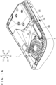
- FIG. 1A is a perspective view illustrating an electronic device 1 that is an example of an embodiment of the present disclosure
- FIG. 1B is a plan view of the electronic device 1.
- FIGS. 1A and 1B illustrate a state in which a cover not illustrated has been removed from the electronic device 1.
- FIGS. 1C and 1D are perspective views illustrating a housing chamber 4 of the electronic device 1 in which a storage medium 100 is to be housed.
- FIGS. 1B to 1D illustrate a state where a memory cover 60 has been removed from the electronic device.
- connectors 3a and 3b are formed on a side surface 1R of the electronic device 1.
- the connectors 3a and 3b are, for example, connectors conforming to the universal serial bus (USB) standard, but the standard of them is not limited to the USB standard.
- USB universal serial bus
- the storage medium 100 such as a solid state drive (SSD) is attached inside the electronic device 1 as indicated by a two-dot chain line in FIG. 1B .
- the electronic device 1 is provided with the housing chamber 4 that is a recess for housing the storage medium 100.
- a Z1 direction (a direction in which the housing chamber 4 opens) and a Z2 direction of a Z axis illustrated in FIG. 1A and other figures are referred to as an upward direction and a downward direction, respectively.
- a Y1 direction and a Y2 direction of a Y axis perpendicular to the Z axis are referred to as a forward direction and a backward direction, respectively.
- an X1 direction and an X2 direction of an X axis perpendicular to the Z axis and the Y axis are referred to as a rightward direction and a leftward direction, respectively.
- these directions are defined to describe shapes and relative positional relations of elements such as components, members, and portions of the electronic device 1 and do not limit the posture of the electronic device 1 during use.
- FIG. 2 is a cross-sectional view of the electronic device 1 obtained by a cross-sectional view including line II-II of FIG. 1B and illustrates a state in which the storage medium 100 and the memory cover 60 are attached to the electronic device 1.
- the housing chamber 4 housing the storage medium 100 is a box-shaped space having a bottom portion, which is defined by an upper surface 40U of a lower board shield 40 and an upper surface 20U of a circuit board 20 to be described later with reference to FIG. 3B , and three walls standing on the front side, back side, and right side of the bottom portion.
- the cover 60 is attached to a housing 70 forming at least part of the housing chamber 4 and covers the housing chamber 4 on the upper side, thereby closing the housing chamber 4.
- the memory cover 60 that covers the housing chamber 4 is fixed to the housing 70 made of an insulating material such as resin, by means of a fixture 6 such as a screw.
- a fixture 6 such as a screw.
- the lower board shield 40 that covers the lower side of the circuit board 20 is placed, and the fixture 6 passes through a mounting hole 72 formed in the housing 70 and is attached to a mounting hole 42 formed in the lower board shield 40.
- the memory cover 60, the fixture 6, and the lower board shield 40 are each made of conductive metal, and these members are electrically connected to each other.
- the storage medium 100 is housed inside the housing chamber 4 covered with the memory cover 60.
- a sponge-like cushion member may be provided between the memory cover 60 and the storage medium 100 to protect the storage medium 100 from impact or the like, or a heat sink may be provided to cool the storage medium 100.
- the storage medium 100 has a circuit board 101.
- the storage medium 100 has areas 102U and 102D in which an integrated circuit mounted on the circuit board 101 and a heat dissipation component and the like attached to the integrated circuit are arranged.
- the storage medium 100 has a first end 100L and a second end 100R located opposite to the first end 100L.
- a terminal part not illustrated is formed at the first end 100L of the storage medium 100.
- a ground part not illustrated is formed at the second end 100R of the storage medium 100.
- the circuit board 101 of the storage medium 100 has the first end 100L and the second end 100R.
- the terminal part and the ground part are conductive wiring or the like mounted on the circuit board 101.
- the first end 100L and the second end 100R of the circuit board 101 protrude in longitudinal directions (X2 direction and X1 direction) of the storage medium 100 beyond the areas 102U and 102D where the integrated circuit and the like are arranged.
- the first end 100L is also simply referred to as the end 100L
- the second end 100R is also simply referred to as the end 100R.
- a connector 3c is provided inside the housing chamber 4 that houses the storage medium 100.
- the connector 3c is provided at one end (the left end) of the housing chamber 4.
- the connector 3c is fitted with the end 100L (see FIG. 2 ) of the storage medium 100 and electrically connected to the terminal part provided on the end 100L.
- the storage medium 100 and the connector 3c are, for example, designed according to the M.2 standard, the standard of the storage medium 100 and the connector 3c is not necessarily limited to the M.2 standard.
- the bottom portion of the housing chamber 4 facing the storage medium 100 attached to the connector 3c is constituted by the upper surface 20U of the circuit board 20 in the vicinity of the connector 3c, and by the upper surface 40U of the lower board shield 40 in the remaining portion.
- a cylindrical spacer 5a is attached inside the housing chamber 4 that houses the storage medium 100.
- At least one positioning portion 4a that defines the position of the spacer 5a is formed on the lower board shield 40 (circuit board shield) to be described later that constitutes the inside of the housing chamber 4.
- the positioning portion 4a is formed on one surface (upper surface 40U illustrated in FIG. 3B ) of the lower board shield 40.
- a plurality of positioning portions 4a are formed on the lower board shield 40 at predetermined intervals in longitudinal directions of the housing chamber 4. One of these positioning portions 4a is selected according to the size of the storage medium 100, and the spacer 5a is attached to the inside of a region R1 determined by the selected positioning portion 4a.
- Each positioning portion 4a formed on the lower board shield 40 is formed integrally with the upper surface 40U of the lower board shield 40 by sheet-metal processing of the lower board shield 40.
- each positioning portion 4a includes a plurality of guide protrusions 4b surrounding the region R1 in which the spacer 5a is to be disposed.
- One positioning portion 4a includes three guide protrusions 4b, and the distance between the guide protrusions 4b included in one positioning portion 4a is smaller than a diameter of a circle defined by an outer edge of the spacer 5a.
- the two or more guide protrusions 4b can make contact with the outer edge of the spacer 5a to guide the spacer 5a to the region R1, thereby facilitating the arrangement of the spacer 5a in the housing chamber 4.
- the spacer 5a can be prevented from moving to the outside of the region R1 defined by the three guide protrusions 4b.
- the number of guide protrusions 4b surrounding the region R1 where the spacer 5a is to be disposed may be two or four. In the case where the number of guide protrusions 4b is two, each of the guide protrusions 4b may surround the region R1 where the spacer 5a is to be disposed, in an arcuate manner in plan view. Also, the number of guide protrusions 4b surrounding the region R1 may be one. In this case, the guide protrusion 4b may surround the region R1 with an arc having a central angle of 180 degrees or more or a full circle in plan view.
- a mounting hole 4c is formed in a central position of the region R1 defined by the positioning portion 4a.
- a fixture 5b such as a screw or a rivet is mounted in a hole formed in the spacer 5a and the mounting hole 4c formed in the lower board shield 40.
- the spacer 5a and the fixture 5b function as a support structure 5 that supports the end 100R of the storage medium 100 in the housing chamber 4.
- the spacer 5a is arranged on the lower board shield 40 forming the housing chamber 4 and makes contact with both the end 100R of the storage medium 100 and the lower board shield 40 at a position between the end 100R and the lower board shield 40.
- the spacer 5a secures a distance between the end 100R of the storage medium 100 and the lower board shield 40.
- the fixture 5b fixes the end 100R of the storage medium 100 to the mounting hole 4c formed in the housing chamber 4. Accordingly, the support structure 5 can support the storage medium 100 and fix the storage medium 100 inside the housing chamber 4.
- the plurality of positioning portions 4a arranged in the rightward and leftward directions are formed on the lower board shield 40 forming the housing chamber 4.
- a plurality of types of storage media 100 having different sizes in the rightward and leftward directions can be supported by the support structure 5 to be fixed inside the housing chamber 4.
- the fixture 5b is made of a conductive material such as metal and is electrically connected to the ground part of the storage medium 100 by coming into contact with the ground part such as a ground pattern mounted on the end 100R of the storage medium 100.
- the ground part is formed on the upper surface of the circuit board 101, and a head portion of the screw, which is the fixture 5b, is electrically connected to the ground part.
- the fixture 5b is in contact with the lower board shield 40 made of a conductive material such as iron or aluminum, at a lower end thereof fitted in the mounting hole 4c, thereby electrically connecting the ground part of the storage medium 100 with the lower board shield 40.
- the spacer 5a may be made of a conductive material.
- the end 100R of the circuit board 101 is sandwiched between the head portion (upper end) of the fixture 5b and an upper end of the spacer 5a, and the spacer 5a makes contact with both the ground part of the storage medium 100 and the lower board shield 40, so that the ground part of the storage medium 100 and the lower board shield 40 may electrically be connected.
- the lower board shield 40 forming the housing chamber 4 is formed with protective protrusions 4d that protrude upward to a position higher than the guide protrusions 4b.
- the protective protrusions 4d extend in the longitudinal directions of the housing chamber 4, namely, in the rightward and leftward directions (directions along the X-axis).
- the protective protrusions 4d are formed on the front and back sides of the plurality of positioning portions 4a arranged in the rightward and leftward directions.
- the protective protrusions 4d prevent the guide protrusions 4b from interfering with the end 100L of the storage medium 100 or components on the storage medium 100 when the end 100L of the storage medium 100 is being attached to the connector 3c.
- the end 100L of the storage medium 100 can be slid leftward while the components mounted on the circuit board 101 of the storage medium 100 are in contact with the protective protrusions 4d, and the end 100L can be fitted into the connector 3c.
- a protrusion 4e protruding upward is formed on the lower board shield 40 constituting the housing chamber 4.
- the protrusion 4e forms a hole 4f having an opening that faces in the leftward direction along the circuit board 20 (X2 direction), namely, in the direction of the connector 3C.
- the storage medium 100 housed in the housing chamber 4 can be cooled by air flowing from the opening of the hole 4f.
- the opening of the hole 4f faces leftward, and the height of the opening can be reduced while securing the area of the opening of the hole 4f. Accordingly, a component (for example, the spacer 5a) can be prevented from falling into the hole 4f.
- the mounting hole 4c formed in the lower board shield 40 also forms an air flow path for cooling the storage medium 100.
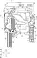
- FIG. 3A is a plan view of a circuit board unit 10 housed inside the electronic device 1.
- FIG. 3B is an exploded perspective view illustrating constituent elements of the circuit board unit 10.
- the circuit board unit 10 has the circuit board 20, an upper board shield 30, the lower board shield 40, and a connector shield 50.
- the circuit board 20 has the upper surface 20U and a lower surface 20D (see FIG. 2 ).
- the upper board shield 30 covers the upper surface 20U of the circuit board 20.
- the lower board shield 40 covers the lower surface 20D of the circuit board 20.
- the connector 3c and a connector 3d which will be described later are mounted on the upper surface 20U of the circuit board 20.
- the connector shield 50 together with the upper board shield 30, covers the upper surface 20U of the circuit board 20.
- the connector shield 50 covers the connectors 3c and 3d mounted on the upper surface 20U of the circuit board 20.
- a plurality of electronic components such as integrated circuit chips 21 are mounted on the upper surface 20U of the circuit board 20.
- a plurality of electronic components are also mounted on the lower surface 20D of the circuit board 20.
- the upper board shield 30 and the lower board shield 40 are provided for suppressing leakage of noise such as electromagnetic waves generated from the plurality of electronic components mounted on the circuit board 20 to the outside of the circuit board unit 10.
- the upper board shield 30 and the lower board shield 40 can be manufactured by performing sheet-metal processing such as drawing processing on a conductive metal plate such as iron or aluminum.
- the upper board shield 30 and the lower board shield 40 are fixed to the circuit board 20 by a plurality of screws, rivets, or the like.
- a heat pipe 8U and a heat sink 9U are attached to the upper board shield 30, and a heat pipe 8D and a heat sink 9D are attached to the lower board shield 40.
- the heat pipe 8D and the heat sink 9D are attached to the lower side of the lower board shield 40.
- FIG. 3C is a perspective view illustrating part of the circuit board unit 10 and illustrates a periphery of the connector 3c mounted on the upper surface 20U of the circuit board 20.
- the connector 3c to which the end 100L of the storage medium 100 is to be attached is mounted on the upper surface 20U of the circuit board 20.
- the support structure 5 for the storage medium 100 including the spacer 5a and the fixture 5b, is arranged outside an outer edge of the circuit board 20 and is positioned away from the connector 3c in the rightward direction (X1 direction, or direction along the circuit board 20).
- the lower board shield 40 has an outer region R2 located outside the outer edge of the circuit board 20, and the support structure 5 is provided in the outer region R2.
- the lower board shield 40 is electrically connected to the ground part of the storage medium 100 via the support structure 5 located in the outer region R2.
- the ground part of the storage medium 100 is connected to a ground pattern formed on a circuit board via the support structure 5 including the spacer 5a and the fixture 5b.
- the ground part of the storage medium 100 makes contact with and is electrically connected to the lower board shield 40, which is a member different from the circuit board 20, through the support structure 5.
- a part that electrically connects to the ground part of the storage medium 100 via the support structure 5 (for example, the mounting hole 4c to which the fixture 5b is attached or the region R1 where the spacer 5a is disposed) is provided on the lower board shield 40, so that the housing chamber 4 for housing the storage medium 100 can be formed by performing sheet-metal processing on the lower board shield 40. That is, formation of the housing chamber 4 can be facilitated.
- the number of members required for manufacturing the electronic device 1 can be reduced compared to the case where the housing chamber 4 is formed of a member different from the constituent elements of the circuit board unit 10.
- the lower board shield 40 has a wall 41F standing along a front side portion (Y1 side portion) of the storage medium 100, a wall 41B standing along a back side portion (Y2 side portion) of the storage medium 100, and a wall 41R standing along the end 100R.
- the housing chamber 4 for housing the storage medium 100 is formed into a box shape having the bottom portion defined by the upper surface 40U of the lower board shield 40 and the upper surface 20U of the circuit board 20, and the walls 41F, 41B, and 41R of the lower board shield 40 surrounding the bottom portion.
- the walls 41F, 41B, and 41R may be formed by subjecting the lower board shield 40 to sheet-metal processing such as bending.
- the upper board shield 30 also has 31BL and 31BR standing along the back side portion (Y2 side portion) of the storage medium 100 and 31F standing along the front side portion (Y1 side portion) of the storage medium 100.
- the walls 31F, 31BL, and 31BR together with the walls 41F, 41B, and 41R of the lower board shield 40 form the box-shaped housing chamber 4. That is, the housing chamber 4 is formed of different components.
- the walls of the housing chamber 4 standing along the sides of the storage medium 100 are configured in such a manner that a portion along an edge of the circuit board 20 is constituted by the upper board shield 30 and the remaining portion is constituted by the lower board shield 40.
- a clearance C1 is formed between the walls 41B and 31BR standing along the back side portion (Y2 side portion), among the walls on the front side and the back side of the storage medium 100. Further, a clearance C2 is formed between the walls 31BR and 31BL, and a clearance C3 is formed between the wall 31BL and the connector shield 50. As illustrated in FIGS. 1C and 1D , walls 71 of the housing 70 are arranged in the clearances C1 to C3. The walls 71 are used for fixing the circuit board unit 10 to the housing 70, for example.
- the housing chamber 4 that houses the storage medium 100 is made of different members.
- the bottom portion of the housing chamber 4 is constituted by the upper surface 20U of the circuit board 20 in the vicinity of the connector 3c, and by the lower board shield 40 covering the circuit board 20 in the remaining portion.
- the cost of the circuit board 20 can be reduced compared to the case where the entire bottom portion of the housing chamber 4 is constituted by the circuit board 20.
- at least part of the bottom portion of the housing chamber 4 may be constructed by the upper board shield 30.
- the connector 3d (first connector) is mounted on the upper surface 20U of the circuit board 20 (first circuit board).
- the upper board shield 30 covers the circuit board 20, and an outer edge of the upper board shield 30 is formed in such a manner as to avoid the connector 3d. That is, in an assembled state of the circuit board unit 10, the connector 3d is exposed in a region R3 defined outside the outer edge of the upper board shield 30 (see FIG. 3B ).
- the connector shield 50 covers the connector 3d mounted on the upper surface 20U of the circuit board 20 in the region R3.
- the connector 3c (third connector) to which the above-described storage medium 100 is to be connected is mounted on the upper surface 20U of the circuit board 20.
- the outer edge of the upper board shield 30 is formed in such a manner as to avoid the connector 3c as well, and the connector 3d is exposed when the circuit board unit 10 is assembled.
- the connector shield 50 covers the connector 3c as well as the connector 3d.
- the connector shield 50 can be manufactured by performing sheet-metal processing such as drawing processing on a conductive metal plate such as iron or aluminum. As illustrated in FIG. 3C , the connector shield 50 has a recess 57 having a dent upward at a position corresponding to the connector 3d. The connector 3d and an end 91 of a flexible flat cable (FFC) 90 attached thereto are housed inside the recess 57.
- FFC flexible flat cable
- a bend 58 that is bent downward is formed on an edge of the connector shield 50.
- the bend 58 of the connector shield 50 abuts against the edge of the upper board shield 30 or the edge of the circuit board 20. This facilitates positioning of the connector shield 50 with respect to the upper board shield 30.
- the connector shield 50 has a guide hole 59 at a position different from the recess 57
- the upper board shield 30 has a guide protrusion 39 projecting upward at a position corresponding to the guide hole 59 of the connector shield 50.
- the guide protrusion 39 of the upper board shield 30 passes through the guide hole 59 of the connector shield 50. This also facilitates positioning of the connector shield 50 with respect to the upper board shield 30.
- FIG. 3D is a perspective view illustrating part of the circuit board 20 and illustrates the periphery of the connectors 3c and 3d mounted on the upper surface 20U of the circuit board 20.
- the connector 3d illustrated in FIG. 3D is a connector that is fitted to the end 91 of the FFC 90 to be described later and electrically connected to the FFC 90.
- the connector 3d has a locking mechanism for fixing the end 91 of the FFC 90 to the connector 3d.
- the locking mechanism of the connector 3d includes a lever Le, and by an operator moving the lever Le to a predetermined fixing position, the end 91 of the FFC 90 is fixed inside the connector 3d.
- the connector shield 50 covers the locking mechanism including the lever Le of the connector 3d.
- the connector shield 50 covers the entire connector 3d.
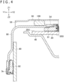
- FIG. 4 is a cross-sectional view of the electronic device 1, obtained by a cross section along line IV-IV in FIG. 3A . Part of the electronic device 1 is omitted in FIG. 4 .
- a conductive elastic member 110 is mounted on the end 91 of the FFC 90.
- the elastic member 110 is in contact with both a ground pattern, not illustrated, provided at the end 91 of the FFC 90 and the connector shield 50.
- the electronic device 1 has a circuit board 80 (second circuit board).
- a connector 3e (second connector) connected to the connector 3d via the FFC 90 is mounted on the circuit board 80.
- the circuit board 80 is arranged on the front side (left side in FIG. 4 ) of the circuit board 20 and arranged along a plane perpendicular to the upper surface 20U and the lower surface 20D of the circuit board 20.
- the circuit board 80 is mounted with the connectors 3a and 3b illustrated in FIG. 1A .
- the connector shield 50 is attached to and removable from the upper board shield 30 by using fixtures 7 such as screws.
- the connector shield 50 has fixing portions 51 such as holes, to be fixed to the upper board shield 30.
- the upper board shield 30 has fixing portions 32 (see FIG. 3B ) such as holes, to be fixed to the connector shield 50 and the circuit board 20, and the circuit board 20 has fixing portions 22 (see FIG. 3D ), to be fixed to the upper board shield 30.
- the fixing portions 22, 32, and 51 are aligned in vertical directions, and one fixture 7 is passed through the corresponding fixing portions 22, 32, and 51 so as to fix the connector shield 50 and the upper board shield 30 to the circuit board 20.
- the connector 3d is covered with the upper board shield 30 that widely covers the circuit board 20, and when the FFC 90 is removed from the connector 3d for repairing the electronic device 1 or the like, the upper board shield 30 needs to be removed. Since the upper board shield 30 is fixed to the circuit board 20 by screws or the like at multiple positions, the work of removing the upper board shield 30 is complicated. In this respect, since the connector 3d is covered with the connector shield 50 different from the upper board shield 30, the FFC 90 can be removed from the connector 3d by removing only the connector shield 50 without removing the upper board shield 30. In other words, provision of the connector shield 50 facilitates removal of the FFC 90 from the connector 3d.
- a ground pattern 23 is formed on the upper surface 20U of the circuit board 20 by using a conductive material.
- the fixing portions 22 to be fixed to the fixing portions 32 of the upper board shield 30 are formed on the ground pattern 23.
- the upper board shield 30 makes contact with the ground pattern 23 on the circuit board 20 at the position of the fixing portions 22 and 32.
- Protrusions 24 protruding upward are formed on the ground pattern 23 formed on the circuit board 20. When the protrusions 24 make contact with the upper board shield 30, noise leakage can more effectively be suppressed.
- One or two protrusions 24 are formed between two adjacent fixing portions 22 formed on the ground pattern 23. The distances between the fixing portion 22 and the protrusion adjacent to each other and between two adjacent protrusions may be set to less than 1/3 of a wavelength of noise shielded by the upper board board shield 30, and more preferably, less than 1/4 of the wavelength.
- the distances between the fixing portion 22 and the protrusion adjacent to each other and between the two adjacent protrusions are set to 20 mm or less, more preferably, 15 mm or less or 10 mm or less, so that leakage of noise of a frequency band desired to be shielded can effectively be suppressed.
- leakage of noise such as electromagnetic waves generated from electronic components mounted on the upper surface 20U of the circuit board 20 to the outside of the circuit board unit 10 can be suppressed at the positions of the fixing portions 22 and 32 and the protrusions 24.
- the noise of the electronic components mounted on the circuit board 20 on an inner side with respect to the ground pattern 23 on the upper surface 20U of the circuit board 20 is shielded by the upper board shield 30, and leakage of noise to the region R3 where the connector 3d is mounted and the area where the connector 3c is mounted is effectively reduced as well.
- one fixing portion 51 of the connector shield 50 is fixed by one fixture 7 to the corresponding fixing portions 22 and 32 to which noise countermeasures have been applied.
- the connector shield 50 by fixing the connector shield 50 by using the fixtures 7 for fixing the upper board shield 30 and the ground pattern 23, the number of fixtures 7 required for the circuit board unit 10 can be reduced.
- the circuit board unit 10 has a region R4 on which electronic components such as integrated circuits on the circuit board 20 are arranged and which is surrounded by a ground part.
- An outer edge of the region R4 is constituted by the ground pattern 23 of the circuit board 20, for example.
- part of the outer edge of the region R4 may be formed by contact portions between a left edge 40L and a right edge 40R of the lower board shield 40 and a left edge 30L and a right edge 30R of the upper board shield 30 illustrated in FIG. 3B . In this manner, noise countermeasures are taken for the electronic components arranged in the region R4.
- the connector shield 50 is arranged outside the region R4 defined on the circuit board 20 in plan view.
- leakage of noise to the outside of the region R4 defined on the circuit board 20 can be suppressed, and the FFC 90 can be removed from the connector 3d by removing only the connector shield 50.
- the fixing portions 51 of the connector shield 50 by fixing the fixing portions 51 of the connector shield 50 by using the plurality of fixtures 7 attached to the fixing portions 22 and 32 for noise countermeasures, the number of fixtures 7 used in the circuit board unit 10 can further be reduced.
- the connector shield 50 that can be attached to and detached from the circuit board 20 and the upper board shield 30 can adopt a shape obtained by taking account of countermeasures against noise generated from the connector 3c or the connector 3d or a shape obtained by taking account of attachment to and detachment from the circuit board 20 or the like. Accordingly, the structure of the connector shield 50 can be simplified.
- FIG. 5 is an enlarged view of part of the cross section illustrated in FIG. 2 and illustrates the periphery of the connector 3c mounted on the upper surface 20U of the circuit board 20.
- the connector 3c has a fitting recess 301 for fitting the end 100L of the storage medium 100 therein.
- the fitting recess 301 opens in the rightward direction along the circuit board 20 (first direction, or direction away from the connector 3c).
- the connector 3c is positioned on one end side (left side) of the housing chamber 4, and the fitting recess 301 opens toward the housing chamber 4.
- FIG. 6 is a front view of the connector viewed in a direction of arrow A in FIG. 5 and illustrates the inside of the fitting recess 301 formed in the connector 3c.
- the connector 3c has a plurality of first signal terminals 302 and a plurality of second signal terminals 304 for electrical connection of the storage medium 100, inside the fitting recess 301.
- each first signal terminal 302 has a terminal part 302a that makes contact with a terminal part provided on the end 100L of the storage medium 100.
- each second signal terminal 304 also has a terminal part 304a that makes contact with a terminal part of the storage medium 100.
- the terminal parts 302a of the plurality of first signal terminals 302 are arranged on the upper side of the fitting recess 301 and arranged in the forward and backward directions (directions along the Y-axis in FIG. 6 ).
- the terminal parts 304a of the plurality of second signal terminals 304 are arranged on the lower side of the fitting recess 301 and arranged in the forward and backward directions.
- the connector 3c has insulating portions 303 each located between two adjacent ones of the plurality of first signal terminals 302.
- the insulating portions 303 are made of an insulating material such as resin and cover the upper side of the plurality of first signal terminals 302.
- a right end 303R of each insulating portion 303 protrudes rightward beyond the terminal parts 302a of the first signal terminals 302 (in an extending direction of the terminal parts 302a, or a direction opposite to a mounting direction of the end 100L of the storage medium 100 into the fitting recess 301).
- each insulating portion 303 protrudes further toward the housing chamber 4 than the terminal parts 302a of the first signal terminals 302. Hence, the insulating portions 303 protect the terminal parts 302a of the first signal terminals 302.
- the connector shield 50 is formed separately from the upper board shield 30 and is attached to the upper board shield 30.
- the connector shield 50 has a dome shape that opens toward the housing chamber 4 in such a manner as to expose the opening of the fitting recess 301 and that entirely covers other portions of the connector 3c.
- the connector shield 50 has an electrostatic protecting portion 52 arranged along the opening of the fitting recess 301 of the connector 3c.
- the connector shield 50 functions as a ground member having the electrostatic protecting portion 52.
- a clearance C4 is formed between the connector 3c and the connector shield 50.
- the connector shield 50 constitutes the ground part of the circuit board unit 10 together with the ground pattern 23 of the circuit board 20, the upper board shield 30, the lower board shield 40, and the like. Therefore, the connector 3c is covered with a ground member different from the connector 3c.
- the electrostatic protecting portion 52 of the connector shield 50 is positioned on the right side (X1 direction) with respect to at least one of the plurality of first signal terminals 302 of the connector 3c.
- the electrostatic protecting portion 52 is positioned on the right side with respect to the terminal part 302a of the first signal terminal 302 that makes contact with the storage medium 100.
- the electrostatic protecting portion 52 may be positioned on the right side with respect to the right end of the entire first signal terminal 302.
- the electrostatic protecting portion 52 may be positioned on the right side with respect to all of the plurality of first signal terminals 302 arranged on the upper side of the fitting recess 301.
- the electrostatic protecting portion 52 of the connector shield 50 is located closer to the housing chamber 4 than at least one of the plurality of first signal terminals 302 of the connector 3c.
- At least one of a plurality of electronic components such as the integrated circuit chips 21 (see FIG. 3B ) mounted on the circuit board 20 functions as a controller that controls the storage medium 100.
- the controller mounted on the circuit board 20 is connected to the storage medium 100 via the connector 3c and controls input/output of signals to/from the storage medium 100.
- circuit board 20 flow of static electricity to the controller can be suppressed, for example, by arranging a diode in an electrical path from the connector 3c to the controller.
- disposing an additional diode on the circuit board 20 is costly.
- a ground member such as the connector shield 50 having the electrostatic protecting portion 52 is provided, and the electrostatic protecting portion 52 is arranged at a position on the right side with respect to the first signal terminals 302 of the connector 3c, so that the static electricity can be received by the connector shield 50.
- the electrostatic protecting portion 52 of the connector shield 50 is positioned closer to the housing chamber 4 (rightward direction) than the right end 303R of the insulating portion 303 located between two adjacent first signal terminals 302. With this positional relation, it can be ensured that the electrostatic protecting portion 52 receives static electricity generated on the operator's finger or the like.
- the connector shield 50 conducts static electricity to the upper board shield 30 to which the connector shield 50 is attached.
- the housing 70 made of an insulating material such as resin has a first wall 73 that defines the housing chamber 4 for housing the storage medium 100.
- the first wall 73 defines an end of an inner surface of the housing chamber 4 close to the connector 3c.
- the electrostatic protecting portion 52 of the connector shield 50 protrudes rightward (X1 direction) further than the first wall 73 of the housing 70.
- the electrostatic protecting portion 52 of the connector shield 50 protrudes into the housing chamber 4. By doing so, the electrostatic protecting portion 52 can receive static electricity generated on the operator's finger or the like.
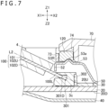
- FIG. 7 is a cross-sectional view corresponding to FIG. 5 and illustrates a state obtained when the storage medium 100 is being mounted to the connector 3c.
- the storage medium 100 can be moved in oblique directions (directions indicated by a dashed-dotted straight line L2) intersecting the rightward and leftward directions (first direction) and the vertical directions (second direction) in such a manner that the end 100L of the storage medium 100 is inserted into the opening of the fitting recess 301.
- the electrostatic protecting portion 52 of the connector shield 50 does not intersect the straight line L2 extending in the oblique directions passing through the fitting recess 301.
- the straight line L2 is, for example, a straight line parallel to a lower surface 301D of the fitting recess 301.
- a distance D1 from the electrostatic protecting portion 52 of the connector shield 50 to the deepest portion of the fitting recess 301 in the rightward and leftward directions is less than 5 mm.
- a distance from an end face of the storage medium 100 (end face of the circuit board 101 facing in the X2 direction) to the component placement area 102U is greater than 5 mm. Therefore, by setting the distance D1 to be smaller than 5 mm, the electrostatic protecting portion 52 can be prevented from interfering with the component placement area 102U of the storage medium 100 while the end 100L of the storage medium 100 is inserted into the deepest portion of the fitting recess 301. More preferably, the distance D1 may be less than 4 mm.
- a tip (free end) of the electrostatic protecting portion 52 of the connector shield 50 is preferably located at a position between the right ends 303R of the insulating portions 303 and the end face, on the connector 3c side, of the component placement area 102U of the storage medium 100 attached to the connector 3c, in the longitudinal directions of the housing chamber 4.
- the connector shield 50 has an upper wall 53 (first wall) that covers the plurality of first signal terminals 302 of the connector 3c. As illustrated in FIGS. 3C , 5 , and 6 , the connector shield 50 has a side wall 54 standing along a side of the connector 3c. The side wall 54 covers a front surface (Y1 side surface), a back surface (Y2 side surface), and a left side surface (X2 side surface) of the connector 3c where the opening of the fitting recess 301 is not formed.
- the electrostatic protecting portion 52 extends vertically (toward the upper surface 20U of the circuit board 20) from an end 53R of the upper wall 53 on the housing chamber 4 side in the rightward direction.
- the electrostatic protecting portion 52 is bent downward from the end 53R of the upper wall 53 toward the connector 3c.
- the tip of the electrostatic protecting portion 52 is preferably positioned above the right ends 303R of the insulating portions 303 in the vertical directions of the housing chamber 4, and is preferably placed at a low position within a range where the tip does not interfere with the storage medium 100 when the storage medium 100 is inserted or removed.
- the clearance C4 (distance) larger than a width D2 of the electrostatic protecting portion 52 in the vertical directions is secured between the upper wall 53 and the connector 3c.
- the clearance C4 between the upper wall 53 and the connector 3c may be equal to the width D2 of the electrostatic protecting portion 52 in the vertical directions.
- the distance of the clearance C4 may be a distance corresponding to the width D2 of the electrostatic protecting portion 52.
- the upper wall 53 of the connector shield 50 has a projecting portion 53a protruding upward.
- the housing 70 has a second wall 74 on the left side of the first wall 73.
- a conductive elastic member 120 is housed in a space defined between the first wall 73 and the second wall 74 of the housing 70. The elastic member 120 is positioned above the upper wall 53 of the connector shield 50.
- the projecting portion 53a formed in the upper wall 53 makes contact with the elastic member 120.
- a right end 60R of the conductive memory cover 60 enters a clearance between the first wall 73 and the second wall 74 of the housing 70 and makes contact with the elastic member 120.
- the memory cover 60 is in contact with the elastic member 120 at the right end 60R and is electrically connected to the elastic member 120.
- the connector shield 50 is in contact with the elastic member 120 at the projecting portion 53a and thus electrically connects with the elastic member 120 and the memory cover 60.
- static electricity is generated on a user's finger or the like when the memory cover 60 is attached or detached, static electricity is allowed to flow through the conductive elastic member 120 and the connector shield 50 to the upper board shield 30 to which the connector shield 50 is attached.
- the ground part provided at the end 100R of the storage medium 100 makes contact with and electrically connects with the lower board shield 40, which is a member different from the circuit board 20, via the support structure 5 including the spacer 5a and the fixture 5b. Due to this, a structure for mounting the support structure 5 and establishing electrical connection via the support structure 5 can be omitted from the circuit board 20, and the cost of the circuit board 20 can be reduced.
- the connector 3d mounted on the upper surface 20U of the circuit board 20 is covered with the connector shield 50 different from the upper board shield 30. Due to this, the FFC 90 can be removed from the connector 3d by removing only the connector shield 50 without removing the upper board shield 30.
- the connector shield 50 has the electrostatic protecting portion 52 arranged along the opening of the fitting recess 301 of the connector 3c to which the storage medium 100 is detachably connected. Due to this, in the case where static electricity is generated on the user's finger or the like when the storage medium 100 is attached or detached, the static electricity can be conducted to the connector shield 50 via the electrostatic protecting portion 52.
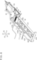
- FIG. 8 is a perspective view illustrating part of the circuit board unit 10 according to a modification and illustrates a periphery of a connector shield 150 attached to the upper board shield 30.
- FIG. 9 is a cross-sectional view of the electronic device 1 around the connector shield 150.
- the connector shield 150 is made of a conductive material and covers the connectors 3c and 3d, similarly to the connector shield 50 described in the above embodiment.
- the shape of a portion covering the connector 3c is different from the shape described in the above embodiment.
- the connector shield 150 has an electrostatic protecting portion 152. Similarly to the example of the connector shield 50, the electrostatic protecting portion 152 is arranged along the opening of the fitting recess 301 of the connector 3c.
- the connector shield 150 has an upper wall 153 (first wall) covering the plurality of first signal terminals 302 of the connector 3c.
- the electrostatic protecting portion 152 is bent upward toward the side opposite to the connector 3c (upper side), from an end 153R of the upper wall 153 in the rightward direction.
- the electrostatic protecting portion 152 of the connector shield 150 is positioned on the right side (X1 direction, or the housing chamber 4 side) with respect to the first signal terminals 302 mounted on the connector 3c. Further, a clearance D5 is formed between the upper wall 153 of the connector shield 150 and the connector 3c. Therefore, static electricity generated from a finger or the like of an operator approaching from the housing chamber 4 side can be received by the electrostatic protecting portion 52 and conducted to the connector shield 50.
- the connector shield 150 includes a folded portion 154 extending leftward from an upper end of the electrostatic protecting portion 152 and a bend 155 bent obliquely upward from a left end of the folded portion 154.
- the connector shield 150 makes contact with the conductive elastic member 120 at the bend 155 and is electrically connected to the elastic member 120.
- the memory cover 60 is in contact with the elastic member 120, and the connector shield 150 is electrically connected to the memory cover 6 via the elastic member 120.
- the example in which the electrostatic protecting portion 52, which receives static electricity, is formed in the connector shield 50 has been described, but a part for receiving static electricity may be provided on a member different from the connector shield 50.
- the upper board shield 30 has the walls 31F and 31BL standing along the sides of the storage medium 100 housed in the housing chamber 4.
- a conductive member for example, a conductive tape
- the conductive member including the portion that receives static electricity may be attached to the lower board shield 40 or may be attached to the upper wall 53 of the connector shield 50 covering the connector 3c.
Landscapes
- Engineering & Computer Science (AREA)
- Theoretical Computer Science (AREA)
- Physics & Mathematics (AREA)
- Human Computer Interaction (AREA)
- General Engineering & Computer Science (AREA)
- General Physics & Mathematics (AREA)
- Computer Hardware Design (AREA)
- Power Engineering (AREA)
- Microelectronics & Electronic Packaging (AREA)
- Electromagnetism (AREA)
- Shielding Devices Or Components To Electric Or Magnetic Fields (AREA)
Abstract
Description
- The present disclosure relates to an electronic device.
- PTL 1 referred to below discloses an electronic device that is able to have a semiconductor memory installed thereon. In recent years, some storage media such as semiconductor memories installed in electronic devices such as game devices and personal computers have a terminal part on one end thereof and a ground part on an opposite end thereof. For example, storage media conforming to the M.2 standard have such a terminal part and a ground part.
-
- In conventional electronic devices, a circuit board has a support structure for supporting an end (an end opposite to a terminal part) of a storage medium. The support structure includes a spacer that defines the height of the end of the storage medium from the circuit board, a screw that secures an end of the circuit board, and the like. The storage medium has a ground part electrically connected to the circuit board through the support structure. For example, the spacer is attached to the circuit board, a hole through which the screw that secures the end of the storage medium is inserted is formed in the circuit board, and the ground part of the storage medium is electrically connected to the circuit board through the spacer and the screw. These structural details have led to an increase in the cost of the circuit board.
- It is an object of the present disclosure to provide an electronic device that can reduce the cost of a circuit board thereof.
- An electronic device according to the present disclosure is an electronic device that is able to have a storage medium installed thereon, the storage medium having a first end with a terminal part formed thereon and a second end opposite to the first end with a ground part formed on the second end, the electronic device including a circuit board having a first surface and a second surface, a connector mounted on the first surface, the first end of the storage medium being connectable to the connector, a support structure that is positioned in a first direction along the circuit board with respect to the connector, that supports the second end, and that is to be connected to the ground part provided on the second end, and a member different from the circuit board and electrically connected to the ground part of the storage medium through the support structure. This electronic device can reduce the cost of the circuit board.
-
- [
FIG. 1A ]
FIG. 1A is a perspective view of an electronic device that is an example of an embodiment of the present disclosure. - [
FIG. 1B ]
FIG. 1B is a plan view of the electronic device. - [
FIG. 1C ]
FIG. 1C is a perspective view illustrating a housing chamber of the electronic device in which a storage medium is to be housed. - [
FIG. 1D ]
FIG. 1D is a perspective view illustrating the housing chamber of the electronic device in which a storage medium is to be housed. - [
FIG. 2 ]
FIG. 2 is a cross-sectional view of the electronic device obtained by a cross-sectional view including line II-II ofFIG. 1B . - [
FIG. 3A ]
FIG. 3A is a plan view of a circuit board unit housed inside the electronic device. - [
FIG. 3B ]
FIG. 3B is an exploded perspective view illustrating constituent elements of the circuit board unit. - [
FIG. 3C ]
FIG. 3C is a perspective view illustrating a peripheral part of a connector in the circuit board unit. - [
FIG. 3D ]
FIG. 3D is a perspective view illustrating the peripheral part of the connector on a circuit board. - [
FIG. 4 ]
FIG. 4 is a cross-sectional view of the electronic device obtained by a cross section along line IV-IV ofFIG. 3A . - [
FIG. 5 ]
FIG. 5 is an enlarged view of a peripheral part of the connector on the cross section illustrated inFIG. 2 . - [
FIG. 6 ]
FIG. 6 is a front view of the connector viewed in a direction of arrow A inFIG. 5 . - [
FIG. 7 ]
FIG. 7 is a cross-sectional view illustrating a state in which a storage medium is being attached to the connector. - [
FIG. 8 ]
FIG. 8 is a perspective view illustrating a periphery of a connector shield in a circuit board unit according to a modification. - [
FIG. 9 ]
FIG. 9 is a cross-sectional view of the electronic device around the connector shield. -
FIG. 1A is a perspective view illustrating an electronic device 1 that is an example of an embodiment of the present disclosure, andFIG. 1B is a plan view of the electronic device 1.FIGS. 1A and1B illustrate a state in which a cover not illustrated has been removed from the electronic device 1.FIGS. 1C and1D are perspective views illustrating ahousing chamber 4 of the electronic device 1 in which astorage medium 100 is to be housed.FIGS. 1B to 1D illustrate a state where amemory cover 60 has been removed from the electronic device. - As illustrated in
FIG. 1A ,connectors side surface 1R of the electronic device 1. Theconnectors - The
storage medium 100 such as a solid state drive (SSD) is attached inside the electronic device 1 as indicated by a two-dot chain line inFIG. 1B . As illustrated inFIGS. 1B to 1D , the electronic device 1 is provided with thehousing chamber 4 that is a recess for housing thestorage medium 100. - In the following description, a Z1 direction (a direction in which the
housing chamber 4 opens) and a Z2 direction of a Z axis illustrated inFIG. 1A and other figures are referred to as an upward direction and a downward direction, respectively. Also, a Y1 direction and a Y2 direction of a Y axis perpendicular to the Z axis are referred to as a forward direction and a backward direction, respectively. Also, an X1 direction and an X2 direction of an X axis perpendicular to the Z axis and the Y axis are referred to as a rightward direction and a leftward direction, respectively. However, these directions are defined to describe shapes and relative positional relations of elements such as components, members, and portions of the electronic device 1 and do not limit the posture of the electronic device 1 during use. -
FIG. 2 is a cross-sectional view of the electronic device 1 obtained by a cross-sectional view including line II-II ofFIG. 1B and illustrates a state in which thestorage medium 100 and thememory cover 60 are attached to the electronic device 1. Thehousing chamber 4 housing thestorage medium 100 is a box-shaped space having a bottom portion, which is defined by anupper surface 40U of alower board shield 40 and anupper surface 20U of acircuit board 20 to be described later with reference toFIG. 3B , and three walls standing on the front side, back side, and right side of the bottom portion. Thecover 60 is attached to ahousing 70 forming at least part of thehousing chamber 4 and covers thehousing chamber 4 on the upper side, thereby closing thehousing chamber 4. - As illustrated in
FIG. 2 , thememory cover 60 that covers thehousing chamber 4 is fixed to thehousing 70 made of an insulating material such as resin, by means of afixture 6 such as a screw. Below thehousing 70, thelower board shield 40 that covers the lower side of thecircuit board 20 is placed, and thefixture 6 passes through a mountinghole 72 formed in thehousing 70 and is attached to a mountinghole 42 formed in thelower board shield 40. Thememory cover 60, thefixture 6, and thelower board shield 40 are each made of conductive metal, and these members are electrically connected to each other. - Moreover, as illustrated in
FIG. 2 , thestorage medium 100 is housed inside thehousing chamber 4 covered with thememory cover 60. Incidentally, a sponge-like cushion member may be provided between thememory cover 60 and thestorage medium 100 to protect thestorage medium 100 from impact or the like, or a heat sink may be provided to cool thestorage medium 100. - As illustrated in
FIG. 2 , thestorage medium 100 has acircuit board 101. Thestorage medium 100 hasareas circuit board 101 and a heat dissipation component and the like attached to the integrated circuit are arranged. Further, thestorage medium 100 has afirst end 100L and asecond end 100R located opposite to thefirst end 100L. A terminal part not illustrated is formed at thefirst end 100L of thestorage medium 100. In addition, a ground part not illustrated is formed at thesecond end 100R of thestorage medium 100. Thecircuit board 101 of thestorage medium 100 has thefirst end 100L and thesecond end 100R. The terminal part and the ground part are conductive wiring or the like mounted on thecircuit board 101. Thefirst end 100L and thesecond end 100R of thecircuit board 101 protrude in longitudinal directions (X2 direction and X1 direction) of thestorage medium 100 beyond theareas first end 100L is also simply referred to as theend 100L, and thesecond end 100R is also simply referred to as theend 100R. - As illustrated in
FIG. 1C , aconnector 3c is provided inside thehousing chamber 4 that houses thestorage medium 100. As illustrated inFIG. 2 , theconnector 3c is provided at one end (the left end) of thehousing chamber 4. Theconnector 3c is fitted with theend 100L (seeFIG. 2 ) of thestorage medium 100 and electrically connected to the terminal part provided on theend 100L. Although thestorage medium 100 and theconnector 3c are, for example, designed according to the M.2 standard, the standard of thestorage medium 100 and theconnector 3c is not necessarily limited to the M.2 standard. The bottom portion of thehousing chamber 4 facing thestorage medium 100 attached to theconnector 3c is constituted by theupper surface 20U of thecircuit board 20 in the vicinity of theconnector 3c, and by theupper surface 40U of thelower board shield 40 in the remaining portion. - As illustrated in
FIG. 1D , acylindrical spacer 5a is attached inside thehousing chamber 4 that houses thestorage medium 100. At least onepositioning portion 4a that defines the position of thespacer 5a is formed on the lower board shield 40 (circuit board shield) to be described later that constitutes the inside of thehousing chamber 4. Thepositioning portion 4a is formed on one surface (upper surface 40U illustrated inFIG. 3B ) of thelower board shield 40. In the example illustrated inFIG. 1D , a plurality ofpositioning portions 4a are formed on thelower board shield 40 at predetermined intervals in longitudinal directions of thehousing chamber 4. One of thesepositioning portions 4a is selected according to the size of thestorage medium 100, and thespacer 5a is attached to the inside of a region R1 determined by the selectedpositioning portion 4a. - Each
positioning portion 4a formed on thelower board shield 40 is formed integrally with theupper surface 40U of thelower board shield 40 by sheet-metal processing of thelower board shield 40. In the example illustrated inFIG. 1D , each positioningportion 4a includes a plurality ofguide protrusions 4b surrounding the region R1 in which thespacer 5a is to be disposed. Onepositioning portion 4a includes threeguide protrusions 4b, and the distance between theguide protrusions 4b included in onepositioning portion 4a is smaller than a diameter of a circle defined by an outer edge of thespacer 5a. Hence, the two ormore guide protrusions 4b can make contact with the outer edge of thespacer 5a to guide thespacer 5a to the region R1, thereby facilitating the arrangement of thespacer 5a in thehousing chamber 4. Moreover, thespacer 5a can be prevented from moving to the outside of the region R1 defined by the threeguide protrusions 4b. - Note that the number of
guide protrusions 4b surrounding the region R1 where thespacer 5a is to be disposed may be two or four. In the case where the number ofguide protrusions 4b is two, each of theguide protrusions 4b may surround the region R1 where thespacer 5a is to be disposed, in an arcuate manner in plan view. Also, the number ofguide protrusions 4b surrounding the region R1 may be one. In this case, theguide protrusion 4b may surround the region R1 with an arc having a central angle of 180 degrees or more or a full circle in plan view. - As illustrated in
FIG. 1D , a mountinghole 4c is formed in a central position of the region R1 defined by thepositioning portion 4a. As illustrated inFIG. 2 , afixture 5b such as a screw or a rivet is mounted in a hole formed in thespacer 5a and the mountinghole 4c formed in thelower board shield 40. Thespacer 5a and thefixture 5b function as asupport structure 5 that supports theend 100R of thestorage medium 100 in thehousing chamber 4. Thespacer 5a is arranged on thelower board shield 40 forming thehousing chamber 4 and makes contact with both theend 100R of thestorage medium 100 and thelower board shield 40 at a position between theend 100R and thelower board shield 40. Thespacer 5a secures a distance between theend 100R of thestorage medium 100 and thelower board shield 40. Thefixture 5b fixes theend 100R of thestorage medium 100 to the mountinghole 4c formed in thehousing chamber 4. Accordingly, thesupport structure 5 can support thestorage medium 100 and fix thestorage medium 100 inside thehousing chamber 4. - As illustrated in
FIG. 1D , the plurality ofpositioning portions 4a arranged in the rightward and leftward directions (directions along the X-axis) are formed on thelower board shield 40 forming thehousing chamber 4. By doing so, a plurality of types ofstorage media 100 having different sizes in the rightward and leftward directions can be supported by thesupport structure 5 to be fixed inside thehousing chamber 4. - The
fixture 5b is made of a conductive material such as metal and is electrically connected to the ground part of thestorage medium 100 by coming into contact with the ground part such as a ground pattern mounted on theend 100R of thestorage medium 100. For example, the ground part is formed on the upper surface of thecircuit board 101, and a head portion of the screw, which is thefixture 5b, is electrically connected to the ground part. Thefixture 5b is in contact with thelower board shield 40 made of a conductive material such as iron or aluminum, at a lower end thereof fitted in the mountinghole 4c, thereby electrically connecting the ground part of thestorage medium 100 with thelower board shield 40. Also, thespacer 5a may be made of a conductive material. Theend 100R of thecircuit board 101 is sandwiched between the head portion (upper end) of thefixture 5b and an upper end of thespacer 5a, and thespacer 5a makes contact with both the ground part of thestorage medium 100 and thelower board shield 40, so that the ground part of thestorage medium 100 and thelower board shield 40 may electrically be connected. - As illustrated in
FIGS. 1C and1D , thelower board shield 40 forming thehousing chamber 4 is formed withprotective protrusions 4d that protrude upward to a position higher than theguide protrusions 4b. On thelower board shield 40, theprotective protrusions 4d extend in the longitudinal directions of thehousing chamber 4, namely, in the rightward and leftward directions (directions along the X-axis). Theprotective protrusions 4d are formed on the front and back sides of the plurality ofpositioning portions 4a arranged in the rightward and leftward directions. Theprotective protrusions 4d prevent theguide protrusions 4b from interfering with theend 100L of thestorage medium 100 or components on thestorage medium 100 when theend 100L of thestorage medium 100 is being attached to theconnector 3c. By forming theprotective protrusions 4d, theend 100L of thestorage medium 100 can be slid leftward while the components mounted on thecircuit board 101 of thestorage medium 100 are in contact with theprotective protrusions 4d, and theend 100L can be fitted into theconnector 3c. - Further, as illustrated in
FIG. 1D , aprotrusion 4e protruding upward is formed on thelower board shield 40 constituting thehousing chamber 4. Theprotrusion 4e forms ahole 4f having an opening that faces in the leftward direction along the circuit board 20 (X2 direction), namely, in the direction of the connector 3C. By doing so, thestorage medium 100 housed in thehousing chamber 4 can be cooled by air flowing from the opening of thehole 4f. Further, by forming thehole 4f by using theprotrusion 4e, the opening of thehole 4f faces leftward, and the height of the opening can be reduced while securing the area of the opening of thehole 4f. Accordingly, a component (for example, thespacer 5a) can be prevented from falling into thehole 4f. The mountinghole 4c formed in thelower board shield 40 also forms an air flow path for cooling thestorage medium 100. -
FIG. 3A is a plan view of acircuit board unit 10 housed inside the electronic device 1.FIG. 3B is an exploded perspective view illustrating constituent elements of thecircuit board unit 10. As illustrated inFIG. 3B , thecircuit board unit 10 has thecircuit board 20, anupper board shield 30, thelower board shield 40, and aconnector shield 50. Thecircuit board 20 has theupper surface 20U and alower surface 20D (seeFIG. 2 ). Theupper board shield 30 covers theupper surface 20U of thecircuit board 20. Thelower board shield 40 covers thelower surface 20D of thecircuit board 20. Theconnector 3c and aconnector 3d which will be described later are mounted on theupper surface 20U of thecircuit board 20. Theconnector shield 50, together with theupper board shield 30, covers theupper surface 20U of thecircuit board 20. Theconnector shield 50 covers theconnectors upper surface 20U of thecircuit board 20. - As illustrated in
FIG. 3B , a plurality of electronic components such asintegrated circuit chips 21 are mounted on theupper surface 20U of thecircuit board 20. A plurality of electronic components are also mounted on thelower surface 20D of thecircuit board 20. Theupper board shield 30 and thelower board shield 40 are provided for suppressing leakage of noise such as electromagnetic waves generated from the plurality of electronic components mounted on thecircuit board 20 to the outside of thecircuit board unit 10. Theupper board shield 30 and thelower board shield 40 can be manufactured by performing sheet-metal processing such as drawing processing on a conductive metal plate such as iron or aluminum. Theupper board shield 30 and thelower board shield 40 are fixed to thecircuit board 20 by a plurality of screws, rivets, or the like. - Incidentally, in the example illustrated in
FIG. 3B , aheat pipe 8U and aheat sink 9U are attached to theupper board shield 30, and aheat pipe 8D and aheat sink 9D are attached to thelower board shield 40. Theheat pipe 8D and theheat sink 9D are attached to the lower side of thelower board shield 40. -
FIG. 3C is a perspective view illustrating part of thecircuit board unit 10 and illustrates a periphery of theconnector 3c mounted on theupper surface 20U of thecircuit board 20. As illustrated inFIG. 3C , theconnector 3c to which theend 100L of thestorage medium 100 is to be attached is mounted on theupper surface 20U of thecircuit board 20. Thesupport structure 5 for thestorage medium 100, including thespacer 5a and thefixture 5b, is arranged outside an outer edge of thecircuit board 20 and is positioned away from theconnector 3c in the rightward direction (X1 direction, or direction along the circuit board 20). As illustrated inFIG. 3A , thelower board shield 40 has an outer region R2 located outside the outer edge of thecircuit board 20, and thesupport structure 5 is provided in the outer region R2. Thelower board shield 40 is electrically connected to the ground part of thestorage medium 100 via thesupport structure 5 located in the outer region R2. - In a related-art electronic device, the ground part of the
storage medium 100 is connected to a ground pattern formed on a circuit board via thesupport structure 5 including thespacer 5a and thefixture 5b. In contrast, in the present embodiment, the ground part of thestorage medium 100 makes contact with and is electrically connected to thelower board shield 40, which is a member different from thecircuit board 20, through thesupport structure 5. By doing so, formation of the ground pattern on thecircuit board 20 can be omitted, and the cost of thecircuit board 20 can be reduced. - In addition, a part that electrically connects to the ground part of the
storage medium 100 via the support structure 5 (for example, the mountinghole 4c to which thefixture 5b is attached or the region R1 where thespacer 5a is disposed) is provided on thelower board shield 40, so that thehousing chamber 4 for housing thestorage medium 100 can be formed by performing sheet-metal processing on thelower board shield 40. That is, formation of thehousing chamber 4 can be facilitated. In addition, for example, the number of members required for manufacturing the electronic device 1 can be reduced compared to the case where thehousing chamber 4 is formed of a member different from the constituent elements of thecircuit board unit 10. - As illustrated in
FIG. 3C , thelower board shield 40 has awall 41F standing along a front side portion (Y1 side portion) of thestorage medium 100, awall 41B standing along a back side portion (Y2 side portion) of thestorage medium 100, and awall 41R standing along theend 100R. Thehousing chamber 4 for housing thestorage medium 100 is formed into a box shape having the bottom portion defined by theupper surface 40U of thelower board shield 40 and theupper surface 20U of thecircuit board 20, and thewalls lower board shield 40 surrounding the bottom portion. Thewalls lower board shield 40 to sheet-metal processing such as bending. - As illustrated in
FIG. 3C , theupper board shield 30 also has 31BL and 31BR standing along the back side portion (Y2 side portion) of thestorage medium storage medium 100. Thewalls 31F, 31BL, and 31BR together with thewalls lower board shield 40 form the box-shapedhousing chamber 4. That is, thehousing chamber 4 is formed of different components. The walls of thehousing chamber 4 standing along the sides of thestorage medium 100 are configured in such a manner that a portion along an edge of thecircuit board 20 is constituted by theupper board shield 30 and the remaining portion is constituted by thelower board shield 40. - As illustrated in
FIG. 3C , a clearance C1 is formed between thewalls 41B and 31BR standing along the back side portion (Y2 side portion), among the walls on the front side and the back side of thestorage medium 100. Further, a clearance C2 is formed between the walls 31BR and 31BL, and a clearance C3 is formed between the wall 31BL and theconnector shield 50. As illustrated inFIGS. 1C and1D ,walls 71 of thehousing 70 are arranged in the clearances C1 to C3. Thewalls 71 are used for fixing thecircuit board unit 10 to thehousing 70, for example. - The
housing chamber 4 that houses thestorage medium 100 is made of different members. As described above, the bottom portion of thehousing chamber 4 is constituted by theupper surface 20U of thecircuit board 20 in the vicinity of theconnector 3c, and by thelower board shield 40 covering thecircuit board 20 in the remaining portion. By doing so, the cost of thecircuit board 20 can be reduced compared to the case where the entire bottom portion of thehousing chamber 4 is constituted by thecircuit board 20. Incidentally, at least part of the bottom portion of thehousing chamber 4 may be constructed by theupper board shield 30. - As illustrated in
FIG. 3B , theconnector 3d (first connector) is mounted on theupper surface 20U of the circuit board 20 (first circuit board). Further, theupper board shield 30 covers thecircuit board 20, and an outer edge of theupper board shield 30 is formed in such a manner as to avoid theconnector 3d. That is, in an assembled state of thecircuit board unit 10, theconnector 3d is exposed in a region R3 defined outside the outer edge of the upper board shield 30 (seeFIG. 3B ). Theconnector shield 50 covers theconnector 3d mounted on theupper surface 20U of thecircuit board 20 in the region R3. Further, theconnector 3c (third connector) to which the above-describedstorage medium 100 is to be connected is mounted on theupper surface 20U of thecircuit board 20. The outer edge of theupper board shield 30 is formed in such a manner as to avoid theconnector 3c as well, and theconnector 3d is exposed when thecircuit board unit 10 is assembled. Theconnector shield 50 covers theconnector 3c as well as theconnector 3d. - The
connector shield 50 can be manufactured by performing sheet-metal processing such as drawing processing on a conductive metal plate such as iron or aluminum. As illustrated inFIG. 3C , theconnector shield 50 has arecess 57 having a dent upward at a position corresponding to theconnector 3d. Theconnector 3d and anend 91 of a flexible flat cable (FFC) 90 attached thereto are housed inside therecess 57. - As illustrated in
FIG. 3C , abend 58 that is bent downward is formed on an edge of theconnector shield 50. Thebend 58 of theconnector shield 50 abuts against the edge of theupper board shield 30 or the edge of thecircuit board 20. This facilitates positioning of theconnector shield 50 with respect to theupper board shield 30. Further, theconnector shield 50 has aguide hole 59 at a position different from therecess 57, and theupper board shield 30 has aguide protrusion 39 projecting upward at a position corresponding to theguide hole 59 of theconnector shield 50. When theconnector shield 50 is disposed on theupper board shield 30, theguide protrusion 39 of theupper board shield 30 passes through theguide hole 59 of theconnector shield 50. This also facilitates positioning of theconnector shield 50 with respect to theupper board shield 30. -
FIG. 3D is a perspective view illustrating part of thecircuit board 20 and illustrates the periphery of theconnectors upper surface 20U of thecircuit board 20. Theconnector 3d illustrated inFIG. 3D is a connector that is fitted to theend 91 of theFFC 90 to be described later and electrically connected to theFFC 90. Theconnector 3d has a locking mechanism for fixing theend 91 of theFFC 90 to theconnector 3d. For example, the locking mechanism of theconnector 3d includes a lever Le, and by an operator moving the lever Le to a predetermined fixing position, theend 91 of theFFC 90 is fixed inside theconnector 3d. Further, by the operator moving the lever Le to a predetermined release position, the fixation of theconnector 3d to theend 91 of theFFC 90 is released. As illustrated inFIGS. 3C and3D , theconnector shield 50 covers the locking mechanism including the lever Le of theconnector 3d. Theconnector shield 50 covers theentire connector 3d. -
FIG. 4 is a cross-sectional view of the electronic device 1, obtained by a cross section along line IV-IV inFIG. 3A . Part of the electronic device 1 is omitted inFIG. 4 . As illustrated inFIG. 3D and4 , a conductiveelastic member 110 is mounted on theend 91 of theFFC 90. Theelastic member 110 is in contact with both a ground pattern, not illustrated, provided at theend 91 of theFFC 90 and theconnector shield 50. Further, as illustrated inFIG. 4 , the electronic device 1 has a circuit board 80 (second circuit board). Aconnector 3e (second connector) connected to theconnector 3d via theFFC 90 is mounted on thecircuit board 80. Thecircuit board 80 is arranged on the front side (left side inFIG. 4 ) of thecircuit board 20 and arranged along a plane perpendicular to theupper surface 20U and thelower surface 20D of thecircuit board 20. Thecircuit board 80 is mounted with theconnectors FIG. 1A . - As illustrated in
FIG. 3C , theconnector shield 50 is attached to and removable from theupper board shield 30 by usingfixtures 7 such as screws. Theconnector shield 50 has fixingportions 51 such as holes, to be fixed to theupper board shield 30. Further, theupper board shield 30 has fixing portions 32 (seeFIG. 3B ) such as holes, to be fixed to theconnector shield 50 and thecircuit board 20, and thecircuit board 20 has fixing portions 22 (seeFIG. 3D ), to be fixed to theupper board shield 30. As illustrated by dashed-dotted straight lines L1 inFIG. 3B , the fixingportions fixture 7 is passed through the corresponding fixingportions connector shield 50 and theupper board shield 30 to thecircuit board 20. - In a related-art structure, the
connector 3d is covered with theupper board shield 30 that widely covers thecircuit board 20, and when theFFC 90 is removed from theconnector 3d for repairing the electronic device 1 or the like, theupper board shield 30 needs to be removed. Since theupper board shield 30 is fixed to thecircuit board 20 by screws or the like at multiple positions, the work of removing theupper board shield 30 is complicated. In this respect, since theconnector 3d is covered with theconnector shield 50 different from theupper board shield 30, theFFC 90 can be removed from theconnector 3d by removing only theconnector shield 50 without removing theupper board shield 30. In other words, provision of theconnector shield 50 facilitates removal of theFFC 90 from theconnector 3d. - As illustrated in
FIG. 3D , aground pattern 23 is formed on theupper surface 20U of thecircuit board 20 by using a conductive material. The fixingportions 22 to be fixed to the fixingportions 32 of theupper board shield 30 are formed on theground pattern 23. By fastening the corresponding fixingportions FIG. 3C ), theupper board shield 30 makes contact with theground pattern 23 on thecircuit board 20 at the position of the fixingportions -
Protrusions 24 protruding upward are formed on theground pattern 23 formed on thecircuit board 20. When theprotrusions 24 make contact with theupper board shield 30, noise leakage can more effectively be suppressed. One or twoprotrusions 24 are formed between twoadjacent fixing portions 22 formed on theground pattern 23. The distances between the fixingportion 22 and the protrusion adjacent to each other and between two adjacent protrusions may be set to less than 1/3 of a wavelength of noise shielded by the upperboard board shield 30, and more preferably, less than 1/4 of the wavelength. For example, the distances between the fixingportion 22 and the protrusion adjacent to each other and between the two adjacent protrusions are set to 20 mm or less, more preferably, 15 mm or less or 10 mm or less, so that leakage of noise of a frequency band desired to be shielded can effectively be suppressed. - In this manner, leakage of noise such as electromagnetic waves generated from electronic components mounted on the
upper surface 20U of thecircuit board 20 to the outside of thecircuit board unit 10 can be suppressed at the positions of the fixingportions protrusions 24. In particular, the noise of the electronic components mounted on thecircuit board 20 on an inner side with respect to theground pattern 23 on theupper surface 20U of thecircuit board 20 is shielded by theupper board shield 30, and leakage of noise to the region R3 where theconnector 3d is mounted and the area where theconnector 3c is mounted is effectively reduced as well. - Further, one fixing
portion 51 of theconnector shield 50 is fixed by onefixture 7 to the corresponding fixingportions connector shield 50 by using thefixtures 7 for fixing theupper board shield 30 and theground pattern 23, the number offixtures 7 required for thecircuit board unit 10 can be reduced. - Further, as illustrated in
FIG. 3B , thecircuit board unit 10 has a region R4 on which electronic components such as integrated circuits on thecircuit board 20 are arranged and which is surrounded by a ground part. An outer edge of the region R4 is constituted by theground pattern 23 of thecircuit board 20, for example. Still further, part of the outer edge of the region R4 may be formed by contact portions between aleft edge 40L and aright edge 40R of thelower board shield 40 and aleft edge 30L and aright edge 30R of theupper board shield 30 illustrated inFIG. 3B . In this manner, noise countermeasures are taken for the electronic components arranged in the region R4. - As illustrated in
FIG. 3D , theconnector shield 50 is arranged outside the region R4 defined on thecircuit board 20 in plan view. By adopting the above layout, leakage of noise to the outside of the region R4 defined on thecircuit board 20 can be suppressed, and theFFC 90 can be removed from theconnector 3d by removing only theconnector shield 50. In addition, by fixing the fixingportions 51 of theconnector shield 50 by using the plurality offixtures 7 attached to the fixingportions fixtures 7 used in thecircuit board unit 10 can further be reduced. - Further, on the
upper surface 20U of thecircuit board 20, noise generated from electronic components mounted inside the region R4 defined by theground pattern 23 is shielded by theupper board shield 30. Therefore, theconnector shield 50 that can be attached to and detached from thecircuit board 20 and theupper board shield 30 can adopt a shape obtained by taking account of countermeasures against noise generated from theconnector 3c or theconnector 3d or a shape obtained by taking account of attachment to and detachment from thecircuit board 20 or the like. Accordingly, the structure of theconnector shield 50 can be simplified. -
FIG. 5 is an enlarged view of part of the cross section illustrated inFIG. 2 and illustrates the periphery of theconnector 3c mounted on theupper surface 20U of thecircuit board 20. As illustrated inFIG. 5 , theconnector 3c has afitting recess 301 for fitting theend 100L of thestorage medium 100 therein. Thefitting recess 301 opens in the rightward direction along the circuit board 20 (first direction, or direction away from theconnector 3c). Theconnector 3c is positioned on one end side (left side) of thehousing chamber 4, and thefitting recess 301 opens toward thehousing chamber 4. -
FIG. 6 is a front view of the connector viewed in a direction of arrow A inFIG. 5 and illustrates the inside of thefitting recess 301 formed in theconnector 3c. As illustrated inFIG. 6 , theconnector 3c has a plurality offirst signal terminals 302 and a plurality ofsecond signal terminals 304 for electrical connection of thestorage medium 100, inside thefitting recess 301. As illustrated inFIG. 5 , eachfirst signal terminal 302 has aterminal part 302a that makes contact with a terminal part provided on theend 100L of thestorage medium 100. Further, as illustrated inFIG. 6 , eachsecond signal terminal 304 also has aterminal part 304a that makes contact with a terminal part of thestorage medium 100. Theterminal parts 302a of the plurality offirst signal terminals 302 are arranged on the upper side of thefitting recess 301 and arranged in the forward and backward directions (directions along the Y-axis inFIG. 6 ). In addition, theterminal parts 304a of the plurality ofsecond signal terminals 304 are arranged on the lower side of thefitting recess 301 and arranged in the forward and backward directions. - As illustrated in
FIG. 6 , theconnector 3c has insulatingportions 303 each located between two adjacent ones of the plurality offirst signal terminals 302. The insulatingportions 303 are made of an insulating material such as resin and cover the upper side of the plurality offirst signal terminals 302. As illustrated inFIG. 5 , aright end 303R of each insulatingportion 303 protrudes rightward beyond theterminal parts 302a of the first signal terminals 302 (in an extending direction of theterminal parts 302a, or a direction opposite to a mounting direction of theend 100L of thestorage medium 100 into the fitting recess 301). In other words, theright end 303R of each insulatingportion 303 protrudes further toward thehousing chamber 4 than theterminal parts 302a of thefirst signal terminals 302. Hence, the insulatingportions 303 protect theterminal parts 302a of thefirst signal terminals 302. - As previously mentioned, the
connector shield 50 is formed separately from theupper board shield 30 and is attached to theupper board shield 30. Theconnector shield 50 has a dome shape that opens toward thehousing chamber 4 in such a manner as to expose the opening of thefitting recess 301 and that entirely covers other portions of theconnector 3c. As illustrated inFIG. 6 , theconnector shield 50 has anelectrostatic protecting portion 52 arranged along the opening of thefitting recess 301 of theconnector 3c. In the present embodiment, theconnector shield 50 functions as a ground member having the electrostatic protectingportion 52. A clearance C4 is formed between theconnector 3c and theconnector shield 50. Theconnector shield 50 constitutes the ground part of thecircuit board unit 10 together with theground pattern 23 of thecircuit board 20, theupper board shield 30, thelower board shield 40, and the like. Therefore, theconnector 3c is covered with a ground member different from theconnector 3c. - As illustrated in
FIG. 5 , the electrostatic protectingportion 52 of theconnector shield 50 is positioned on the right side (X1 direction) with respect to at least one of the plurality offirst signal terminals 302 of theconnector 3c. To be more specific, the electrostatic protectingportion 52 is positioned on the right side with respect to theterminal part 302a of thefirst signal terminal 302 that makes contact with thestorage medium 100. Theelectrostatic protecting portion 52 may be positioned on the right side with respect to the right end of the entirefirst signal terminal 302. Also, the electrostatic protectingportion 52 may be positioned on the right side with respect to all of the plurality offirst signal terminals 302 arranged on the upper side of thefitting recess 301. In other words, the electrostatic protectingportion 52 of theconnector shield 50 is located closer to thehousing chamber 4 than at least one of the plurality offirst signal terminals 302 of theconnector 3c. When an operator attaches or detaches thestorage medium 100 to or from theconnector 3c, the operator's finger moves from thehousing chamber 4 toward theconnector 3c together with thestorage medium 100, so that static electricity can be conducted from the operator's finger to the electrostatic protectingportion 52 by providing the electrostatic protectingportion 52 on thehousing chamber 4 side. - At least one of a plurality of electronic components such as the integrated circuit chips 21 (see
FIG. 3B ) mounted on thecircuit board 20 functions as a controller that controls thestorage medium 100. The controller mounted on thecircuit board 20 is connected to thestorage medium 100 via theconnector 3c and controls input/output of signals to/from thestorage medium 100. When replacing thestorage medium 100, it is necessary to take measures to protect theconnector 3c and the controller from static electricity generated on the operator's finger or the like. - In the
circuit board 20, flow of static electricity to the controller can be suppressed, for example, by arranging a diode in an electrical path from theconnector 3c to the controller. However, disposing an additional diode on thecircuit board 20 is costly. In contrast, as in the present embodiment, a ground member such as theconnector shield 50 having the electrostatic protectingportion 52 is provided, and the electrostatic protectingportion 52 is arranged at a position on the right side with respect to thefirst signal terminals 302 of theconnector 3c, so that the static electricity can be received by theconnector shield 50. As a result, there is no need to provide a diode in the electrical path leading to the controller, and the cost of thecircuit board 20 can be reduced. - As illustrated in
FIG. 5 , the electrostatic protectingportion 52 of theconnector shield 50 is positioned closer to the housing chamber 4 (rightward direction) than theright end 303R of the insulatingportion 303 located between two adjacentfirst signal terminals 302. With this positional relation, it can be ensured that the electrostatic protectingportion 52 receives static electricity generated on the operator's finger or the like. Theconnector shield 50 conducts static electricity to theupper board shield 30 to which theconnector shield 50 is attached. - As illustrated in
FIG. 5 , thehousing 70 made of an insulating material such as resin has afirst wall 73 that defines thehousing chamber 4 for housing thestorage medium 100. Thefirst wall 73 defines an end of an inner surface of thehousing chamber 4 close to theconnector 3c. Theelectrostatic protecting portion 52 of theconnector shield 50 protrudes rightward (X1 direction) further than thefirst wall 73 of thehousing 70. Theelectrostatic protecting portion 52 of theconnector shield 50 protrudes into thehousing chamber 4. By doing so, the electrostatic protectingportion 52 can receive static electricity generated on the operator's finger or the like. -
FIG. 7 is a cross-sectional view corresponding toFIG. 5 and illustrates a state obtained when thestorage medium 100 is being mounted to theconnector 3c. As illustrated inFIG. 7 , thestorage medium 100 can be moved in oblique directions (directions indicated by a dashed-dotted straight line L2) intersecting the rightward and leftward directions (first direction) and the vertical directions (second direction) in such a manner that theend 100L of thestorage medium 100 is inserted into the opening of thefitting recess 301. Theelectrostatic protecting portion 52 of theconnector shield 50 does not intersect the straight line L2 extending in the oblique directions passing through thefitting recess 301. The straight line L2 is, for example, a straight line parallel to alower surface 301D of thefitting recess 301. By doing so, when thestorage medium 100 is mounted to theconnector 3c, while the electrostatic protectingportion 52 is prevented from interfering with theend 100L of thestorage medium 100, theend 100L can be inserted into thefitting recess 301 in the oblique direction. - As illustrated in
FIG. 5 , a distance D1 from the electrostatic protectingportion 52 of theconnector shield 50 to the deepest portion of thefitting recess 301 in the rightward and leftward directions is less than 5 mm. In general, a distance from an end face of the storage medium 100 (end face of thecircuit board 101 facing in the X2 direction) to thecomponent placement area 102U is greater than 5 mm. Therefore, by setting the distance D1 to be smaller than 5 mm, the electrostatic protectingportion 52 can be prevented from interfering with thecomponent placement area 102U of thestorage medium 100 while theend 100L of thestorage medium 100 is inserted into the deepest portion of thefitting recess 301. More preferably, the distance D1 may be less than 4 mm. A tip (free end) of the electrostatic protectingportion 52 of theconnector shield 50 is preferably located at a position between the right ends 303R of the insulatingportions 303 and the end face, on theconnector 3c side, of thecomponent placement area 102U of thestorage medium 100 attached to theconnector 3c, in the longitudinal directions of thehousing chamber 4. - The
connector shield 50 has an upper wall 53 (first wall) that covers the plurality offirst signal terminals 302 of theconnector 3c. As illustrated inFIGS. 3C ,5 , and6 , theconnector shield 50 has aside wall 54 standing along a side of theconnector 3c. Theside wall 54 covers a front surface (Y1 side surface), a back surface (Y2 side surface), and a left side surface (X2 side surface) of theconnector 3c where the opening of thefitting recess 301 is not formed. - In the
connector shield 50, the electrostatic protectingportion 52 extends vertically (toward theupper surface 20U of the circuit board 20) from anend 53R of theupper wall 53 on thehousing chamber 4 side in the rightward direction. Theelectrostatic protecting portion 52 is bent downward from theend 53R of theupper wall 53 toward theconnector 3c. The tip of the electrostatic protectingportion 52 is preferably positioned above the right ends 303R of the insulatingportions 303 in the vertical directions of thehousing chamber 4, and is preferably placed at a low position within a range where the tip does not interfere with thestorage medium 100 when thestorage medium 100 is inserted or removed. Hence, the clearance C4 (distance) larger than a width D2 of the electrostatic protectingportion 52 in the vertical directions is secured between theupper wall 53 and theconnector 3c. By securing the large clearance C4 between theconnector 3c and theupper wall 53 in this manner, the static electricity received by the electrostatic protectingportion 52 can be allowed to flow through theupper wall 53 along a path away from theconnector 3c. Incidentally, the clearance C4 between theupper wall 53 and theconnector 3c may be equal to the width D2 of the electrostatic protectingportion 52 in the vertical directions. In other words, the distance of the clearance C4 may be a distance corresponding to the width D2 of the electrostatic protectingportion 52. - As illustrated in
FIGS. 3C and5 , theupper wall 53 of theconnector shield 50 has a projectingportion 53a protruding upward. As illustrated inFIG. 5 , thehousing 70 has asecond wall 74 on the left side of thefirst wall 73. Further, a conductiveelastic member 120 is housed in a space defined between thefirst wall 73 and thesecond wall 74 of thehousing 70. Theelastic member 120 is positioned above theupper wall 53 of theconnector shield 50. The projectingportion 53a formed in theupper wall 53 makes contact with theelastic member 120. - As illustrated in
FIG. 5 , aright end 60R of theconductive memory cover 60 enters a clearance between thefirst wall 73 and thesecond wall 74 of thehousing 70 and makes contact with theelastic member 120. Thememory cover 60 is in contact with theelastic member 120 at theright end 60R and is electrically connected to theelastic member 120. Also, theconnector shield 50 is in contact with theelastic member 120 at the projectingportion 53a and thus electrically connects with theelastic member 120 and thememory cover 60. In the case where static electricity is generated on a user's finger or the like when thememory cover 60 is attached or detached, static electricity is allowed to flow through the conductiveelastic member 120 and theconnector shield 50 to theupper board shield 30 to which theconnector shield 50 is attached. - As described above, in the present embodiment, the ground part provided at the
end 100R of thestorage medium 100 makes contact with and electrically connects with thelower board shield 40, which is a member different from thecircuit board 20, via thesupport structure 5 including thespacer 5a and thefixture 5b. Due to this, a structure for mounting thesupport structure 5 and establishing electrical connection via thesupport structure 5 can be omitted from thecircuit board 20, and the cost of thecircuit board 20 can be reduced. - Further, in the present embodiment, the
connector 3d mounted on theupper surface 20U of thecircuit board 20 is covered with theconnector shield 50 different from theupper board shield 30. Due to this, theFFC 90 can be removed from theconnector 3d by removing only theconnector shield 50 without removing theupper board shield 30. - In addition, in the present embodiment, the
connector shield 50 has the electrostatic protectingportion 52 arranged along the opening of thefitting recess 301 of theconnector 3c to which thestorage medium 100 is detachably connected. Due to this, in the case where static electricity is generated on the user's finger or the like when thestorage medium 100 is attached or detached, the static electricity can be conducted to theconnector shield 50 via the electrostatic protectingportion 52. - In addition, the present disclosure is not limited to the above embodiment.
- (1) In the embodiment, the example in which the ground part of the
storage medium 100 is electrically connected to thelower board shield 40 via thesupport structure 5 has been described. Alternatively, the ground part of thestorage medium 100 may be electrically connected to a member different from thecircuit board 20 and thelower board shield 40. For example, the ground part of thestorage medium 100 may be electrically connected to theupper board shield 30. This can also omit the structure for attaching thesupport structure 5 or establishing electrical connection via thesupport structure 5 from thecircuit board 20, and the cost of thecircuit board 20 can be reduced. - (2) In the embodiment, the example in which the
connector 3d connected to theend 91 of theFFC 90 is mounted on theupper surface 20U of thecircuit board 20 has been described. Alternatively, theconnector 3d may be mounted on thelower surface 20D (seeFIG. 4 ) of thecircuit board 20. In this case, theconnector shield 50 may be attached to thelower board shield 40 and may cover theconnector 3d exposed from thelower board shield 40 on thelower surface 20D of thecircuit board 20. With such an arrangement, too, theFFC 90 can be removed from theconnector 3d by removing only theconnector shield 50 without removing thelower board shield 40, and theFFC 90 can easily be removed from theconnector 3d. - (3) In the embodiment, the example in which the electrostatic protecting
portion 52 that receives static electricity in theconnector shield 50 is bent downward from theend 53R of theupper wall 53 has been described. The shape of theconnector shield 50 including the electrostatic protectingportion 52 is not limited to this example. -
FIG. 8 is a perspective view illustrating part of thecircuit board unit 10 according to a modification and illustrates a periphery of aconnector shield 150 attached to theupper board shield 30.FIG. 9 is a cross-sectional view of the electronic device 1 around theconnector shield 150. As illustrated inFIG. 8 , theconnector shield 150 is made of a conductive material and covers theconnectors connector shield 50 described in the above embodiment. However, in theconnector shield 150, the shape of a portion covering theconnector 3c is different from the shape described in the above embodiment. - As illustrated in
FIG. 9 , theconnector shield 150 has anelectrostatic protecting portion 152. Similarly to the example of theconnector shield 50, theelectrostatic protecting portion 152 is arranged along the opening of thefitting recess 301 of theconnector 3c. Theconnector shield 150 has an upper wall 153 (first wall) covering the plurality offirst signal terminals 302 of theconnector 3c. Theelectrostatic protecting portion 152 is bent upward toward the side opposite to theconnector 3c (upper side), from anend 153R of theupper wall 153 in the rightward direction. - The
electrostatic protecting portion 152 of theconnector shield 150 is positioned on the right side (X1 direction, or thehousing chamber 4 side) with respect to thefirst signal terminals 302 mounted on theconnector 3c. Further, a clearance D5 is formed between theupper wall 153 of theconnector shield 150 and theconnector 3c. Therefore, static electricity generated from a finger or the like of an operator approaching from thehousing chamber 4 side can be received by the electrostatic protectingportion 52 and conducted to theconnector shield 50. - Further, as illustrated in
FIG. 9 , theconnector shield 150 includes a foldedportion 154 extending leftward from an upper end of theelectrostatic protecting portion 152 and abend 155 bent obliquely upward from a left end of the foldedportion 154. Theconnector shield 150 makes contact with the conductiveelastic member 120 at thebend 155 and is electrically connected to theelastic member 120. Further, thememory cover 60 is in contact with theelastic member 120, and theconnector shield 150 is electrically connected to thememory cover 6 via theelastic member 120. - (4) In the embodiment, the example in which the electrostatic protecting
portion 52, which receives static electricity, is formed in theconnector shield 50 has been described, but a part for receiving static electricity may be provided on a member different from theconnector shield 50. As illustrated inFIG. 3C , theupper board shield 30 has thewalls 31F and 31BL standing along the sides of thestorage medium 100 housed in thehousing chamber 4. Here, a conductive member (for example, a conductive tape) including a portion that receives static electricity may be attached to thewalls 31F and 31BL of theupper board shield 30. Alternatively, the conductive member including the portion that receives static electricity may be attached to thelower board shield 40 or may be attached to theupper wall 53 of theconnector shield 50 covering theconnector 3c. With such an arrangement, too, static electricity can be conducted to theupper board shield 30 and thelower board shield 40 more quickly by arranging the portion that receives static electricity near an edge of the opening of thehousing chamber 4.
Claims (12)
- An electronic device that is able to have a storage medium installed thereon, the storage medium having a first end with a terminal part formed thereon and a second end opposite to the first end with a ground part formed on the second end, the electronic device comprising:a circuit board having a first surface and a second surface;a connector mounted on the first surface, the first end of the storage medium being connectable to the connector;a support structure that is positioned in a first direction along the circuit board with respect to the connector, that supports the second end, and that is to be connected to the ground part provided on the second end; anda member different from the circuit board and electrically connected to the ground part of the storage medium through the support structure.
- The electronic device according to claim 1, wherein the member different from the circuit board is a circuit board shield covering the second surface of the circuit board.
- The electronic device according to claim 2, wherein the circuit board shield has a wall standing along a side portion of the storage medium.
- The electronic device according to claim 1, wherein the member different from the circuit board has an outer region located outside of an outer edge of the circuit board, and
the support structure is provided in the outer region. - The electronic device according to claim 1, wherein the support structure includes a spacer that secures a distance between the member different from the circuit board and the second end of the storage medium.
- The electronic device according to claim 5, wherein the member different from the circuit board has a mounting hole defined therein, and
the support structure has a fixture that fixes the second end of the storage medium to the mounting hole and that is held in contact with the ground part of the storage medium. - The electronic device according to claim 5, wherein the member different from the circuit board has at least one positioning portion formed thereon that defines a position of the spacer.
- The electronic device according to claim 7, wherein the member different from the circuit board has a plurality of positioning portions formed thereon that are arranged in the first direction, as the at least one positioning portion.
- The electronic device according to claim 8, wherein the at least one positioning portion includes one or a plurality of protrusions surrounding a region in which the spacer is disposed.
- The electronic device according to claim 9, wherein the member different from the circuit board has a protrusion formed thereon that extends in the first direction.
- The electronic device according to claim 1, wherein the member different from the circuit board has a hole defined therein that is open in a direction along the circuit board.
- The electronic device according to claim 7, wherein the member different from the circuit board is a circuit board shield covering the second surface of the circuit board, and the at least one positioning portion is integrally formed with a surface of the circuit board shield.
Applications Claiming Priority (2)
| Application Number | Priority Date | Filing Date | Title |
|---|---|---|---|
| JP2022065376 | 2022-04-11 | ||
| PCT/JP2023/013180 WO2023199752A1 (en) | 2022-04-11 | 2023-03-30 | Electronic device |
Publications (2)
| Publication Number | Publication Date |
|---|---|
| EP4510800A1 true EP4510800A1 (en) | 2025-02-19 |
| EP4510800A4 EP4510800A4 (en) | 2026-04-08 |
Family
ID=88329226
Family Applications (2)
| Application Number | Title | Priority Date | Filing Date |
|---|---|---|---|
| EP23788028.1A Pending EP4510796A4 (en) | 2022-04-11 | 2023-02-21 | ELECTRONIC DEVICE |
| EP23788172.7A Pending EP4510800A4 (en) | 2022-04-11 | 2023-03-30 | ELECTRONIC DEVICE |
Family Applications Before (1)
| Application Number | Title | Priority Date | Filing Date |
|---|---|---|---|
| EP23788028.1A Pending EP4510796A4 (en) | 2022-04-11 | 2023-02-21 | ELECTRONIC DEVICE |
Country Status (5)
| Country | Link |
|---|---|
| US (1) | US20250298446A1 (en) |
| EP (2) | EP4510796A4 (en) |
| JP (2) | JP7824406B2 (en) |
| CN (2) | CN118872397A (en) |
| WO (2) | WO2023199605A1 (en) |
Families Citing this family (2)
| Publication number | Priority date | Publication date | Assignee | Title |
|---|---|---|---|---|
| KR20230112396A (en) * | 2022-01-20 | 2023-07-27 | 에스케이하이닉스 주식회사 | Solid state drive to avoid electromagnetic interference by changing the length of bottom plane |
| TWI901553B (en) * | 2025-04-18 | 2025-10-11 | 雙鴻科技股份有限公司 | Heat dissipation module |
Family Cites Families (10)
| Publication number | Priority date | Publication date | Assignee | Title |
|---|---|---|---|---|
| JPH01273392A (en) * | 1988-04-26 | 1989-11-01 | Canon Inc | Electronic equipment |
| JP2553438Y2 (en) * | 1989-04-27 | 1997-11-05 | 日本エー・エム・ピー 株式会社 | Memory card connector |
| US20040255313A1 (en) * | 2003-06-10 | 2004-12-16 | Kaczeus Steven L. | Protecting a data storage device |
| CN109673124A (en) | 2017-10-17 | 2019-04-23 | 鸿富锦精密工业(武汉)有限公司 | Circuit board and electronic equipment |
| TWM561980U (en) * | 2017-12-05 | 2018-06-11 | 技嘉科技股份有限公司 | Main circuit board with heat dissipation holes and electronic device thereof |
| US11520381B2 (en) * | 2020-03-19 | 2022-12-06 | Nexark, Inc. | Enclosing a portable solid state device |
| CN115299192B (en) | 2020-03-27 | 2025-07-04 | 索尼互动娱乐股份有限公司 | Electronic devices |
| JP7203784B2 (en) * | 2020-03-27 | 2023-01-13 | 株式会社ソニー・インタラクティブエンタテインメント | Electronic equipment and its outer panel |
| US12028975B2 (en) * | 2020-11-09 | 2024-07-02 | Samsung Electronics Co., Ltd. | Electronic device including shielding member |
| CN217306766U (en) * | 2022-02-23 | 2022-08-26 | 鸿富锦精密工业(武汉)有限公司 | SSD card switching support and circuit board assembly |
-
2023
- 2023-02-21 EP EP23788028.1A patent/EP4510796A4/en active Pending
- 2023-02-21 WO PCT/JP2023/006288 patent/WO2023199605A1/en not_active Ceased
- 2023-02-21 JP JP2024514823A patent/JP7824406B2/en active Active
- 2023-02-21 CN CN202380026658.7A patent/CN118872397A/en active Pending
- 2023-02-21 US US18/854,998 patent/US20250298446A1/en active Pending
- 2023-03-30 WO PCT/JP2023/013180 patent/WO2023199752A1/en not_active Ceased
- 2023-03-30 EP EP23788172.7A patent/EP4510800A4/en active Pending
- 2023-03-30 JP JP2024514883A patent/JP7732086B2/en active Active
- 2023-03-30 CN CN202380028759.8A patent/CN118901289A/en active Pending
Also Published As
| Publication number | Publication date |
|---|---|
| WO2023199605A1 (en) | 2023-10-19 |
| US20250298446A1 (en) | 2025-09-25 |
| JP7732086B2 (en) | 2025-09-01 |
| JPWO2023199752A1 (en) | 2023-10-19 |
| JPWO2023199605A1 (en) | 2023-10-19 |
| CN118901289A (en) | 2024-11-05 |
| EP4510796A1 (en) | 2025-02-19 |
| EP4510800A4 (en) | 2026-04-08 |
| JP7824406B2 (en) | 2026-03-04 |
| EP4510796A4 (en) | 2026-02-25 |
| CN118872397A (en) | 2024-10-29 |
| WO2023199752A1 (en) | 2023-10-19 |
Similar Documents
| Publication | Publication Date | Title |
|---|---|---|
| US20230327354A1 (en) | Electronic device | |
| US5999365A (en) | Electromagnetic shielding apparatus for a memory storage disk module which permits air flow for cooling | |
| US20140202755A1 (en) | Receptacle cage, receptacle assembly, and transceiver module assembly | |
| EP4510796A1 (en) | Electronic apparatus | |
| JP2000347767A (en) | Computer system housing | |
| US20110226523A1 (en) | Electronic device | |
| CN110568910A (en) | Vehicle host and vehicle computer system | |
| TW202145665A (en) | Emi shielding for a receptacle cage | |
| CN118572411B (en) | Signal connector and server | |
| US6403879B1 (en) | Electronic chassis having an EMI gasket and integral ventilation holes | |
| WO2014141493A1 (en) | Receptacle assembly and transceiver module assembly | |
| CN104602502B (en) | Cable back board system with electromagnetic radiation absorber | |
| EP4510797A1 (en) | Electronic device | |
| US7525818B1 (en) | Memory card connector with EMI shielding | |
| US20070093135A1 (en) | Enclosure with emi shield | |
| TW200922439A (en) | Electronic circuit mould | |
| JP5022800B2 (en) | Electronics | |
| US20050106938A1 (en) | On-board connector, mating connector adapted to make a connection with the on-board connector, and connector apparatus equipped with the on-board connector and the mating connector | |
| JP3370280B2 (en) | Narrow-pitch multistage board connector and shield shell fittings used therefor | |
| CN220711809U (en) | Domain controller and vehicle | |
| CN223871034U (en) | PCIe device with heat dissipation function | |
| TWI859001B (en) | Cable connector assembly and assembly method thereof | |
| CN115052446B (en) | Electronic equipment | |
| TW202105855A (en) | Connector component including a metal shielding cover having a cover body, a back cover and a grounding part | |
| JP2019192711A (en) | Wiring member fixing structure of electronic apparatus housing, wiring member fixing method and electronic apparatus or video acoustic equipment using the same |
Legal Events
| Date | Code | Title | Description |
|---|---|---|---|
| STAA | Information on the status of an ep patent application or granted ep patent |
Free format text: STATUS: THE INTERNATIONAL PUBLICATION HAS BEEN MADE |
|
| PUAI | Public reference made under article 153(3) epc to a published international application that has entered the european phase |
Free format text: ORIGINAL CODE: 0009012 |
|
| STAA | Information on the status of an ep patent application or granted ep patent |
Free format text: STATUS: REQUEST FOR EXAMINATION WAS MADE |
|
| 17P | Request for examination filed |
Effective date: 20241028 |
|
| AK | Designated contracting states |
Kind code of ref document: A1 Designated state(s): AL AT BE BG CH CY CZ DE DK EE ES FI FR GB GR HR HU IE IS IT LI LT LU LV MC ME MK MT NL NO PL PT RO RS SE SI SK SM TR |
|
| DAV | Request for validation of the european patent (deleted) | ||
| DAX | Request for extension of the european patent (deleted) | ||
| A4 | Supplementary search report drawn up and despatched |
Effective date: 20260306 |
|
| RIC1 | Information provided on ipc code assigned before grant |
Ipc: H05K 9/00 20060101AFI20260302BHEP Ipc: G06F 1/18 20060101ALI20260302BHEP Ipc: H01R 12/73 20110101ALI20260302BHEP Ipc: H01R 13/6594 20110101ALI20260302BHEP Ipc: G06F 1/185 20260101ALI20260302BHEP Ipc: H01R 12/83 20110101ALI20260302BHEP Ipc: H01R 13/648 20060101ALI20260302BHEP Ipc: G06F 1/20 20060101ALI20260302BHEP |