EP4510453A1 - Switch trigger for suppressing inrush current - Google Patents
Switch trigger for suppressing inrush current Download PDFInfo
- Publication number
- EP4510453A1 EP4510453A1 EP23206692.8A EP23206692A EP4510453A1 EP 4510453 A1 EP4510453 A1 EP 4510453A1 EP 23206692 A EP23206692 A EP 23206692A EP 4510453 A1 EP4510453 A1 EP 4510453A1
- Authority
- EP
- European Patent Office
- Prior art keywords
- switch
- terminal
- voltage
- output
- electrically connected
- Prior art date
- Legal status (The legal status is an assumption and is not a legal conclusion. Google has not performed a legal analysis and makes no representation as to the accuracy of the status listed.)
- Granted
Links
Images



Classifications
-
- H—ELECTRICITY
- H03—ELECTRONIC CIRCUITRY
- H03K—PULSE TECHNIQUE
- H03K17/00—Electronic switching or gating, i.e. not by contact-making and –breaking
- H03K17/08—Modifications for protecting switching circuit against overcurrent or overvoltage
- H03K17/081—Modifications for protecting switching circuit against overcurrent or overvoltage without feedback from the output circuit to the control circuit
-
- H—ELECTRICITY
- H02—GENERATION; CONVERSION OR DISTRIBUTION OF ELECTRIC POWER
- H02M—APPARATUS FOR CONVERSION BETWEEN AC AND AC, BETWEEN AC AND DC, OR BETWEEN DC AND DC, AND FOR USE WITH MAINS OR SIMILAR POWER SUPPLY SYSTEMS; CONVERSION OF DC OR AC INPUT POWER INTO SURGE OUTPUT POWER; CONTROL OR REGULATION THEREOF
- H02M3/00—Conversion of DC power input into DC power output
- H02M3/02—Conversion of DC power input into DC power output without intermediate conversion into AC
- H02M3/04—Conversion of DC power input into DC power output without intermediate conversion into AC by static converters
- H02M3/10—Conversion of DC power input into DC power output without intermediate conversion into AC by static converters using discharge tubes with control electrode or semiconductor devices with control electrode
- H02M3/145—Conversion of DC power input into DC power output without intermediate conversion into AC by static converters using discharge tubes with control electrode or semiconductor devices with control electrode using devices of a triode or transistor type requiring continuous application of a control signal
- H02M3/155—Conversion of DC power input into DC power output without intermediate conversion into AC by static converters using discharge tubes with control electrode or semiconductor devices with control electrode using devices of a triode or transistor type requiring continuous application of a control signal using semiconductor devices only
- H02M3/156—Conversion of DC power input into DC power output without intermediate conversion into AC by static converters using discharge tubes with control electrode or semiconductor devices with control electrode using devices of a triode or transistor type requiring continuous application of a control signal using semiconductor devices only with automatic control of output voltage or current, e.g. switching regulators
- H02M3/158—Conversion of DC power input into DC power output without intermediate conversion into AC by static converters using discharge tubes with control electrode or semiconductor devices with control electrode using devices of a triode or transistor type requiring continuous application of a control signal using semiconductor devices only with automatic control of output voltage or current, e.g. switching regulators including plural semiconductor devices as final control devices for a single load
-
- H—ELECTRICITY
- H03—ELECTRONIC CIRCUITRY
- H03K—PULSE TECHNIQUE
- H03K17/00—Electronic switching or gating, i.e. not by contact-making and –breaking
- H03K17/16—Modifications for eliminating interference voltages or currents
- H03K17/161—Modifications for eliminating interference voltages or currents in field-effect transistor switches
- H03K17/165—Modifications for eliminating interference voltages or currents in field-effect transistor switches by feedback from the output circuit to the control circuit
-
- H—ELECTRICITY
- H02—GENERATION; CONVERSION OR DISTRIBUTION OF ELECTRIC POWER
- H02M—APPARATUS FOR CONVERSION BETWEEN AC AND AC, BETWEEN AC AND DC, OR BETWEEN DC AND DC, AND FOR USE WITH MAINS OR SIMILAR POWER SUPPLY SYSTEMS; CONVERSION OF DC OR AC INPUT POWER INTO SURGE OUTPUT POWER; CONTROL OR REGULATION THEREOF
- H02M1/00—Details of apparatus for conversion
- H02M1/0048—Circuits or arrangements for reducing losses
-
- H—ELECTRICITY
- H02—GENERATION; CONVERSION OR DISTRIBUTION OF ELECTRIC POWER
- H02M—APPARATUS FOR CONVERSION BETWEEN AC AND AC, BETWEEN AC AND DC, OR BETWEEN DC AND DC, AND FOR USE WITH MAINS OR SIMILAR POWER SUPPLY SYSTEMS; CONVERSION OF DC OR AC INPUT POWER INTO SURGE OUTPUT POWER; CONTROL OR REGULATION THEREOF
- H02M1/00—Details of apparatus for conversion
- H02M1/0048—Circuits or arrangements for reducing losses
- H02M1/0054—Transistor switching losses
- H02M1/0058—Transistor switching losses by employing soft switching techniques, i.e. commutation of transistors when applied voltage is zero or when current flow is zero
-
- H—ELECTRICITY
- H02—GENERATION; CONVERSION OR DISTRIBUTION OF ELECTRIC POWER
- H02M—APPARATUS FOR CONVERSION BETWEEN AC AND AC, BETWEEN AC AND DC, OR BETWEEN DC AND DC, AND FOR USE WITH MAINS OR SIMILAR POWER SUPPLY SYSTEMS; CONVERSION OF DC OR AC INPUT POWER INTO SURGE OUTPUT POWER; CONTROL OR REGULATION THEREOF
- H02M1/00—Details of apparatus for conversion
- H02M1/08—Circuits specially adapted for the generation of control voltages for semiconductor devices incorporated in static converters
- H02M1/088—Circuits specially adapted for the generation of control voltages for semiconductor devices incorporated in static converters for the simultaneous control of series or parallel connected semiconductor devices
-
- H—ELECTRICITY
- H02—GENERATION; CONVERSION OR DISTRIBUTION OF ELECTRIC POWER
- H02M—APPARATUS FOR CONVERSION BETWEEN AC AND AC, BETWEEN AC AND DC, OR BETWEEN DC AND DC, AND FOR USE WITH MAINS OR SIMILAR POWER SUPPLY SYSTEMS; CONVERSION OF DC OR AC INPUT POWER INTO SURGE OUTPUT POWER; CONTROL OR REGULATION THEREOF
- H02M1/00—Details of apparatus for conversion
- H02M1/32—Means for protecting converters other than automatic disconnection
- H02M1/325—Means for protecting converters other than automatic disconnection with means for allowing continuous operation despite a fault, i.e. fault tolerant converters
-
- H—ELECTRICITY
- H03—ELECTRONIC CIRCUITRY
- H03K—PULSE TECHNIQUE
- H03K17/00—Electronic switching or gating, i.e. not by contact-making and –breaking
- H03K17/08—Modifications for protecting switching circuit against overcurrent or overvoltage
- H03K17/081—Modifications for protecting switching circuit against overcurrent or overvoltage without feedback from the output circuit to the control circuit
- H03K17/08104—Modifications for protecting switching circuit against overcurrent or overvoltage without feedback from the output circuit to the control circuit in field-effect transistor switches
-
- H—ELECTRICITY
- H03—ELECTRONIC CIRCUITRY
- H03K—PULSE TECHNIQUE
- H03K17/00—Electronic switching or gating, i.e. not by contact-making and –breaking
- H03K17/08—Modifications for protecting switching circuit against overcurrent or overvoltage
- H03K17/081—Modifications for protecting switching circuit against overcurrent or overvoltage without feedback from the output circuit to the control circuit
- H03K17/08112—Modifications for protecting switching circuit against overcurrent or overvoltage without feedback from the output circuit to the control circuit in bipolar transistor switches
-
- H—ELECTRICITY
- H03—ELECTRONIC CIRCUITRY
- H03K—PULSE TECHNIQUE
- H03K17/00—Electronic switching or gating, i.e. not by contact-making and –breaking
- H03K17/08—Modifications for protecting switching circuit against overcurrent or overvoltage
- H03K17/081—Modifications for protecting switching circuit against overcurrent or overvoltage without feedback from the output circuit to the control circuit
- H03K17/08116—Modifications for protecting switching circuit against overcurrent or overvoltage without feedback from the output circuit to the control circuit in composite switches
-
- H—ELECTRICITY
- H03—ELECTRONIC CIRCUITRY
- H03K—PULSE TECHNIQUE
- H03K17/00—Electronic switching or gating, i.e. not by contact-making and –breaking
- H03K17/13—Modifications for switching at zero crossing
- H03K17/133—Modifications for switching at zero crossing in field-effect transistor switches
-
- H—ELECTRICITY
- H02—GENERATION; CONVERSION OR DISTRIBUTION OF ELECTRIC POWER
- H02M—APPARATUS FOR CONVERSION BETWEEN AC AND AC, BETWEEN AC AND DC, OR BETWEEN DC AND DC, AND FOR USE WITH MAINS OR SIMILAR POWER SUPPLY SYSTEMS; CONVERSION OF DC OR AC INPUT POWER INTO SURGE OUTPUT POWER; CONTROL OR REGULATION THEREOF
- H02M1/00—Details of apparatus for conversion
- H02M1/32—Means for protecting converters other than automatic disconnection
- H02M1/327—Means for protecting converters other than automatic disconnection against abnormal temperatures
-
- H—ELECTRICITY
- H03—ELECTRONIC CIRCUITRY
- H03K—PULSE TECHNIQUE
- H03K2217/00—Indexing scheme related to electronic switching or gating, i.e. not by contact-making or -breaking covered by H03K17/00
- H03K2217/0036—Means reducing energy consumption
Definitions
- the present disclosure relates to a switch trigger, and more particularly to a switch trigger for suppressing an inrush current.
- a conventional switch control method may suppress inrush current by soft start of switches.
- the switch since a duration for turning on the switch increases, the switch must bear more heat losses, which not only reduces an efficiency but also makes the switch more susceptible to damage.
- a duration for turning off the switch also increases. Therefore, the longer duration for turning off the switch may cause the switch unable to be turned off immediately for implementing protection.
- the present disclosure provides a switch trigger which reduces a voltage variation while turning on a switch by precharge, thereby suppressing an inrush current. Consequently, the problems like efficiency reduction, switch damage, and an inability to turn off the switch immediately while triggering the protection, which are caused by the increased duration for switching the switch in conventional approach, are avoided. Moreover, in the present disclosure, the switch trigger is able to realize zero-voltage switching and has a function of short circuit protection.
- a switch trigger includes an input terminal, an output terminal, a first switch, a bypass resistor, an output capacitor, a diode, a second switch, a discharging resistor, a first divider resistor, and a second divider resistor.
- the first switch has a first terminal and a second terminal respectively and electrically connected to the input terminal and the output terminal.
- the bypass resistor has two terminals respectively and electrically connected to the input terminal and the output terminal.
- the output capacitor has two terminals respectively and electrically connected to the output terminal and a ground terminal.
- the diode has an anode electrically connected to the input terminal.
- the second switch has a first terminal and a second terminal respectively and electrically connected to a cathode of the diode and a third terminal of the first switch.
- the discharging resistor has two terminals respectively and electrically connected to the third terminal of the first switch and the ground terminal.
- the first divider resistor and the second divider resistor are electrically connected in series between the output terminal and the ground terminal, and a connection node between the first divider resistor and the second divider resistor is electrically connected to a third terminal of the second switch.
- FIG. 1 is a schematic circuit diagram illustrating a switch trigger according to a first embodiment of the present disclosure.
- the switch trigger 1 includes an input terminal 11, an output terminal 12, a first switch Q1, a bypass resistor R1, an output capacitor Co, a diode D, a second switch Q2, a discharging resistor R2, a first divider resistor R3, a second divider resistor R4, an input capacitor Cin, and a back-stage detection circuit 13.
- the first divider resistor R3 and the second divider resistor R4 form a voltage divider.
- the input terminal 11 is configured to receive an input voltage Vin
- the output terminal 12 is configured to provide an output voltage Vo.
- First and second terminals of the first switch Q1 are electrically connected to the input terminal 11 and the output terminal 12, respectively.
- Two terminals of the bypass resistor R1 are electrically connected to the input terminal 11 and the output terminal 12, respectively.
- Two terminals of the output capacitor Co are electrically connected to the output terminal 12 and a ground terminal, respectively.
- An anode of diode D is electrically connected to the input terminal 11, and the diode D is configured to prevent current backflow.
- First and second terminals of the second switch Q2 are electrically connected to a cathode of the diode D and a third terminal of the first switch Q1, respectively.
- Two terminals of the discharging resistor R2 are electrically connected to the third terminal of the first switch Q1 and the ground terminal, respectively.
- the first divider resistor R3 and the second divider resistor R4 are electrically connected in series between the output terminal 12 and the ground terminal.
- the first divider resistor R3 and the second divider resistor R4 are respectively coupled to the output terminal 12 and the ground terminal, and a connection node between the first divider resistor R3 and the second divider resistor R4 is electrically connected to a third terminal of the second switch Q2.
- Two terminals of the input capacitor Cin are respectively and electrically connected to the input terminal 11 and the ground terminal, and the input capacitor is configured for decoupling.
- the first switch Q1 turns off, and the input voltage Vin charges the output capacitor Co through the bypass resistor R1 to gradually increase the output voltage Vo at the output terminal 12.
- the second switch Q2 turns on so that the input voltage Vin builds up a voltage Vg across the discharging resistor R2.
- the first divider resistor R3 and the second divider resistor R4 divide the output voltage Vo to generate the voltage Vsen.
- the voltage Vsen increases to a threshold sufficient to turn off the second switch Q2
- the voltage Vg is discharged to the ground terminal through the discharging resistor R2, which causes the first switch Q1 to turn on.
- the first switch Q1 turns on, the input voltage Vin is transmitted to the output terminal 12 to serve as the output voltage Vo.
- the voltage at the output terminal 12 has already been increased by charging the output capacitor Co through the bypass resistor R1. Therefore, when the first switch Q1 turns on, a voltage difference between the input terminal 11 and the output terminal 12 has been reduced already, and thus the inrush current caused by a large voltage difference is prevented. Further, as the voltage at the output terminal 12 gradually increases, a voltage at the second terminal of the first switch Q1 also increases gradually. When the first switch Q1 turns on, a voltage difference between the first and second terminals of first switch Q1 has been reduced already. Accordingly, the inrush current is suppressed, and a body diode of the switch Q1 is prevented from being damaged by an induced electromotive force generated due to Faraday's law of electromagnetic induction.
- the switch trigger 1 further includes a back-stage detection circuit 13 electrically connected to the voltage divider.
- the back-stage detection circuit 13 is configured to provide a back-stage voltage V2nd to the voltage Vsen for adjusting a duration for turning on the first switch Q1.
- the back-stage detection circuit 13 includes a detection capacitor C1, a detection resistor R5, and a detection terminal 14. Two terminals of the detection capacitor C1 are electrically connected to the third terminal of the second switch Q2 and the detection terminal 14, respectively. Two terminals of the detection resistor R5 are electrically connected to the detection terminal 14 and the ground terminal, respectively.
- the detection terminal 14 is configured to detect an output voltage of a back-stage converter.
- the back-stage converter converts the output voltage Vo provided by the switch trigger 1 at the output terminal 12 into the back-stage voltage V2nd.
- the detection terminal 14 is electrically connected to the back-stage voltage V2nd to detect the output voltage of the back-stage converter.
- the back-stage voltage V2nd causes an instant voltage across the detection capacitor C1 and meanwhile changes the voltage Vsen.
- a turn-off timing of the second switch Q2 is advanced, which advances a turn-on timing of the first switch Q1.
- the switch trigger may be disposed in a first-stage power protector to prevent the inrush current when the power supply is powering up.
- a reference voltage e.g., 80% or 90% of the input voltage Vin
- the back-stage converter begins to draw the output voltage Vo to perform voltage conversion. Therefore, it is necessary to advance the turn-on timing of the first switch Q1 to provide the enough output voltage Vo for the back-stage converter to operate normally.
- the first switch Q1 may be a P-type MOSFET (metal-oxide-semiconductor field effect transistor), and the first, second and third terminals of the first switch Q1 are a source, drain and gate, respectively.
- the second switch Q2 may be a P-type BJT (bipolar junction transistor), and the first, second and third terminals of the second switch Q2 are an emitter, collector and base, respectively.
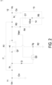
- FIG. 2 is a schematic circuit diagram illustrating a switch trigger according to a second embodiment of the present disclosure.
- a second switch Q3 replaces the second switch Q2 of FIG. 1 .
- the second switch Q3 is a P-type MOSFET, and first, second and third terminals of the second switch Q3 are a source, a drain and a gate, respectively.
- FIG. 3A and FIG. 3B exemplify the key voltage and current waveforms of the switch trigger 1 of FIG. 1 while realizing the inrush current suppression.
- Vg represents the voltage at the third terminal of the first switch Q1
- Vsen represents the voltage at the third terminal of the second switch Q2.
- Iin, I1 and Io represent currents flowing through the first switch Q1, the bypass resistor R1 and the output capacitor Co, respectively.
- the input terminal 11 starts to receive the input voltage Vin (i.e., the input voltage Vin increases)
- the input voltage Vin is provided to the second switch Q2 through the diode D.
- the second switch Q2 is in an on state, resulting in a high level of the voltage Vg at the third terminal of the first switch Q1, and the first switch Q1 is in an off state.
- the input voltage Vin charges the output capacitor Co through the bypass resistor R1, thereby gradually increasing the output voltage Vo across the output capacitor Co.
- the output voltage Vo is lower than the threshold voltage
- the first switch Q1 remains in the off state
- the second switch Q2 remains in the on state
- the output capacitor Co is charged continuously to increase the output voltage Vo gradually.
- the second switch Q2 When the output voltage Vo reaches to the threshold voltage, the second switch Q2 turns off, the voltage Vg at the third terminal of the first switch Q1 is discharged to zero through the discharging resistor R2, and the first switch Q1 turns on. Accordingly, the input voltage Vin is provided to the output terminal 12 through the first switch Q1.
- a person skilled in the art may choose resistance values of the first divider resistor R3 and the second divider resistor R4 according to practical requirements. By changing the resistance values of the first divider resistor R3 and the second divider resistor R4, the turn-off timing of the second switch Q2 is determined. Additionally, in this embodiment, the back-stage converter is not in operation, and thus the back-stage voltage V2nd is fixed at zero.
- FIG. 4A and FIG. 4B exemplify the key voltage and current waveforms of the switch trigger 1 of FIG. 1 while advancing the turn-on timing of the first switch Q1 for corresponding the operation of the back-stage converter.
- Vin the input voltage Vin
- the second switch Q2 is in the on state
- the first switch Q1 is in the off state.
- the input voltage Vin charges the output capacitor Co through the bypass resistor R1, thereby gradually increasing the output voltage Vo across the output capacitor Co.
- the back-stage converter converts the output voltage Vo into the back-stage voltage V2nd.
- the back-stage voltage V2nd is transmitted to the third terminal of the second switch Q2 through the back-stage detection circuit 13, and the voltage Vsen at the third terminal of the second switch Q2 is increased by the back-stage voltage V2nd and triggers the second switch Q2 to turn off.
- the voltage Vg at the third terminal of the first switch Q1 is discharged to zero through the discharging resistor R2, and the first switch Q1 turns on. Accordingly, the input voltage Vin is provided to the output terminal 12 through the first switch Q1.
- the reference voltage is usually lower than the threshold voltage. Therefore, compared with the embodiment shown in FIG. 3A and FIG.
- the turn-off timing of the second switch Q2 is advanced due to the operation of the back-stage converter, and thus the turn-on timing of the first switch Q1 is advanced as well. Electric energy is provided to the back-stage converter through the first switch Q1 such that the back-stage converter is able to operate stably.
- the reference voltage is equal to 80% or 90% of the input voltage Vin, but not limited thereto.
- FIG. 5A and FIG. 5B exemplify the key voltage and current waveforms of the switch trigger 1 of FIG. 1 while implementing the short-circuit protection for the short circuit occurring at the output.
- FIG. 5A and FIG. 5B when the input terminal 11 receives the input voltage Vin and the output terminal 12 is short-circuited to the ground terminal, the output voltage Vo becomes zero, the second switch Q2 remains in the on state, and the voltage Vg at the third terminal of first switch Q1 remains at the high level.
- the first switch Q1 remains in the off state and would not be triggered to turn on, and thus the short-circuit protection is achieved.
- the present disclosure provides a switch trigger which reduces the voltage variation while turning on the switch by precharge, thereby suppressing the inrush current. Consequently, the problems like efficiency reduction, switch damage, and the inability to turn off the switch immediately while triggering the protection, which are caused by the increased time for switching the switch in conventional approach, are avoided.
- the switch trigger is able to realize zero-voltage switching and has the function of short circuit protection. Further, the switch trigger can ensure the stable output of the back-stage converter.
Landscapes
- Engineering & Computer Science (AREA)
- Power Engineering (AREA)
- Dc-Dc Converters (AREA)
- Electronic Switches (AREA)
- Direct Current Feeding And Distribution (AREA)
Abstract
Description
- The present disclosure relates to a switch trigger, and more particularly to a switch trigger for suppressing an inrush current.
- A conventional switch control method may suppress inrush current by soft start of switches. However, since a duration for turning on the switch increases, the switch must bear more heat losses, which not only reduces an efficiency but also makes the switch more susceptible to damage. In addition, as the duration for turning on the switch increases, a duration for turning off the switch also increases. Therefore, the longer duration for turning off the switch may cause the switch unable to be turned off immediately for implementing protection.
- Therefore, there is a need of providing a switch trigger in order to overcome the drawbacks of the conventional technologies.
- The present disclosure provides a switch trigger which reduces a voltage variation while turning on a switch by precharge, thereby suppressing an inrush current. Consequently, the problems like efficiency reduction, switch damage, and an inability to turn off the switch immediately while triggering the protection, which are caused by the increased duration for switching the switch in conventional approach, are avoided. Moreover, in the present disclosure, the switch trigger is able to realize zero-voltage switching and has a function of short circuit protection.
- In accordance with an aspect of the present disclosure, a switch trigger is provided. The switch trigger includes an input terminal, an output terminal, a first switch, a bypass resistor, an output capacitor, a diode, a second switch, a discharging resistor, a first divider resistor, and a second divider resistor. The first switch has a first terminal and a second terminal respectively and electrically connected to the input terminal and the output terminal. The bypass resistor has two terminals respectively and electrically connected to the input terminal and the output terminal. The output capacitor has two terminals respectively and electrically connected to the output terminal and a ground terminal. The diode has an anode electrically connected to the input terminal. The second switch has a first terminal and a second terminal respectively and electrically connected to a cathode of the diode and a third terminal of the first switch. The discharging resistor has two terminals respectively and electrically connected to the third terminal of the first switch and the ground terminal. The first divider resistor and the second divider resistor are electrically connected in series between the output terminal and the ground terminal, and a connection node between the first divider resistor and the second divider resistor is electrically connected to a third terminal of the second switch.
-
-
FIG. 1 is a schematic circuit diagram illustrating a switch trigger according to a first embodiment of the present disclosure; -
FIG. 2 is a schematic circuit diagram illustrating a switch trigger according to a second embodiment of the present disclosure; -
FIG. 3A andFIG. 3B exemplify the key voltage and current waveforms of the switch trigger ofFIG. 1 while realizing the inrush current suppression; -
FIG. 4A andFIG. 4B exemplify the key voltage and current waveforms of the switch trigger ofFIG. 1 while advancing the turn-on timing of the first switch for corresponding the operation of the back-stage converter; and -
FIG. 5A andFIG. 5B exemplify the key voltage and current waveforms of the switch trigger ofFIG. 1 while implementing the short-circuit protection for the short circuit occurring at the output. - The present disclosure will now be described more specifically with reference to the following embodiments. It is to be noted that the following descriptions of preferred embodiments of this disclosure are presented herein for purpose of illustration and description only. It is not intended to be exhaustive or to be limited to the precise form disclosed.
-
FIG. 1 is a schematic circuit diagram illustrating a switch trigger according to a first embodiment of the present disclosure. As shown inFIG. 1 , theswitch trigger 1 includes aninput terminal 11, anoutput terminal 12, a first switch Q1, a bypass resistor R1, an output capacitor Co, a diode D, a second switch Q2, a discharging resistor R2, a first divider resistor R3, a second divider resistor R4, an input capacitor Cin, and a back-stage detection circuit 13. The first divider resistor R3 and the second divider resistor R4 form a voltage divider. - Structurally, the
input terminal 11 is configured to receive an input voltage Vin, and theoutput terminal 12 is configured to provide an output voltage Vo. First and second terminals of the first switch Q1 are electrically connected to theinput terminal 11 and theoutput terminal 12, respectively. Two terminals of the bypass resistor R1 are electrically connected to theinput terminal 11 and theoutput terminal 12, respectively. Two terminals of the output capacitor Co are electrically connected to theoutput terminal 12 and a ground terminal, respectively. An anode of diode D is electrically connected to theinput terminal 11, and the diode D is configured to prevent current backflow. First and second terminals of the second switch Q2 are electrically connected to a cathode of the diode D and a third terminal of the first switch Q1, respectively. Two terminals of the discharging resistor R2 are electrically connected to the third terminal of the first switch Q1 and the ground terminal, respectively. The first divider resistor R3 and the second divider resistor R4 are electrically connected in series between theoutput terminal 12 and the ground terminal. The first divider resistor R3 and the second divider resistor R4 are respectively coupled to theoutput terminal 12 and the ground terminal, and a connection node between the first divider resistor R3 and the second divider resistor R4 is electrically connected to a third terminal of the second switch Q2. Two terminals of the input capacitor Cin are respectively and electrically connected to theinput terminal 11 and the ground terminal, and the input capacitor is configured for decoupling. - In operation, when initially power up, the first switch Q1 turns off, and the input voltage Vin charges the output capacitor Co through the bypass resistor R1 to gradually increase the output voltage Vo at the
output terminal 12. At the same time, the second switch Q2 turns on so that the input voltage Vin builds up a voltage Vg across the discharging resistor R2. Afterwards, the first divider resistor R3 and the second divider resistor R4 divide the output voltage Vo to generate the voltage Vsen. When the voltage Vsen increases to a threshold sufficient to turn off the second switch Q2, the voltage Vg is discharged to the ground terminal through the discharging resistor R2, which causes the first switch Q1 to turn on. As the first switch Q1 turns on, the input voltage Vin is transmitted to theoutput terminal 12 to serve as the output voltage Vo. - It is noted that the voltage at the
output terminal 12 has already been increased by charging the output capacitor Co through the bypass resistor R1. Therefore, when the first switch Q1 turns on, a voltage difference between theinput terminal 11 and theoutput terminal 12 has been reduced already, and thus the inrush current caused by a large voltage difference is prevented. Further, as the voltage at theoutput terminal 12 gradually increases, a voltage at the second terminal of the first switch Q1 also increases gradually. When the first switch Q1 turns on, a voltage difference between the first and second terminals of first switch Q1 has been reduced already. Accordingly, the inrush current is suppressed, and a body diode of the switch Q1 is prevented from being damaged by an induced electromotive force generated due to Faraday's law of electromagnetic induction. - The
switch trigger 1 further includes a back-stage detection circuit 13 electrically connected to the voltage divider. The back-stage detection circuit 13 is configured to provide a back-stage voltage V2nd to the voltage Vsen for adjusting a duration for turning on the first switch Q1. The back-stage detection circuit 13 includes a detection capacitor C1, a detection resistor R5, and adetection terminal 14. Two terminals of the detection capacitor C1 are electrically connected to the third terminal of the second switch Q2 and thedetection terminal 14, respectively. Two terminals of the detection resistor R5 are electrically connected to thedetection terminal 14 and the ground terminal, respectively. Thedetection terminal 14 is configured to detect an output voltage of a back-stage converter. For example, when theoutput terminal 12 is electrically connected to the back-stage converter (not shown), the back-stage converter converts the output voltage Vo provided by theswitch trigger 1 at theoutput terminal 12 into the back-stage voltage V2nd. Thedetection terminal 14 is electrically connected to the back-stage voltage V2nd to detect the output voltage of the back-stage converter. The back-stage voltage V2nd causes an instant voltage across the detection capacitor C1 and meanwhile changes the voltage Vsen. As a result, a turn-off timing of the second switch Q2 is advanced, which advances a turn-on timing of the first switch Q1. - In multi-level power conversion systems, the switch trigger may be disposed in a first-stage power protector to prevent the inrush current when the power supply is powering up. In order to expedite a power-up process of the entire system, as soon as the output voltage Vo reaches to a reference voltage (e.g., 80% or 90% of the input voltage Vin), the back-stage converter begins to draw the output voltage Vo to perform voltage conversion. Therefore, it is necessary to advance the turn-on timing of the first switch Q1 to provide the enough output voltage Vo for the back-stage converter to operate normally.
- In the first embodiment, the first switch Q1 may be a P-type MOSFET (metal-oxide-semiconductor field effect transistor), and the first, second and third terminals of the first switch Q1 are a source, drain and gate, respectively. The second switch Q2 may be a P-type BJT (bipolar junction transistor), and the first, second and third terminals of the second switch Q2 are an emitter, collector and base, respectively.
-
FIG. 2 is a schematic circuit diagram illustrating a switch trigger according to a second embodiment of the present disclosure. InFIG. 2 , a second switch Q3 replaces the second switch Q2 ofFIG. 1 . The second switch Q3 is a P-type MOSFET, and first, second and third terminals of the second switch Q3 are a source, a drain and a gate, respectively. - Please refer to
FIG. 1 ,FIG. 3A andFIG. 3B .FIG. 3A andFIG. 3B exemplify the key voltage and current waveforms of theswitch trigger 1 ofFIG. 1 while realizing the inrush current suppression. InFIG. 3A , Vg represents the voltage at the third terminal of the first switch Q1, and Vsen represents the voltage at the third terminal of the second switch Q2. InFIG. 3B , Iin, I1 and Io represent currents flowing through the first switch Q1, the bypass resistor R1 and the output capacitor Co, respectively. As shown inFIG. 1 ,FIG. 3A andFIG. 3B , when theinput terminal 11 starts to receive the input voltage Vin (i.e., the input voltage Vin increases), the input voltage Vin is provided to the second switch Q2 through the diode D. At this time, the second switch Q2 is in an on state, resulting in a high level of the voltage Vg at the third terminal of the first switch Q1, and the first switch Q1 is in an off state. Under this circumstance, the input voltage Vin charges the output capacitor Co through the bypass resistor R1, thereby gradually increasing the output voltage Vo across the output capacitor Co. When the output voltage Vo is lower than the threshold voltage, the first switch Q1 remains in the off state, the second switch Q2 remains in the on state, and the output capacitor Co is charged continuously to increase the output voltage Vo gradually. When the output voltage Vo reaches to the threshold voltage, the second switch Q2 turns off, the voltage Vg at the third terminal of the first switch Q1 is discharged to zero through the discharging resistor R2, and the first switch Q1 turns on. Accordingly, the input voltage Vin is provided to theoutput terminal 12 through the first switch Q1. It is noted that a person skilled in the art may choose resistance values of the first divider resistor R3 and the second divider resistor R4 according to practical requirements. By changing the resistance values of the first divider resistor R3 and the second divider resistor R4, the turn-off timing of the second switch Q2 is determined. Additionally, in this embodiment, the back-stage converter is not in operation, and thus the back-stage voltage V2nd is fixed at zero. - Consequently, zero-voltage turn-on for the first switch Q1 is realized, and thus the switch loss is reduced. Further, since the output voltage Vo is already at a higher level when the first switch Q1 turns on, the voltage variation is decreased and the inrush current is reduced, thereby realizing inrush current suppression.
- Please refer to
FIG. 1 ,FIG. 4A andFIG. 4B .FIG. 4A andFIG. 4B exemplify the key voltage and current waveforms of theswitch trigger 1 ofFIG. 1 while advancing the turn-on timing of the first switch Q1 for corresponding the operation of the back-stage converter. As shown inFIG. 1 ,FIG. 4A andFIG. 4B , when theinput terminal 11 starts to receive the input voltage Vin (i.e., the input voltage Vin increases), the second switch Q2 is in the on state, and the first switch Q1 is in the off state. Under this circumstance, the input voltage Vin charges the output capacitor Co through the bypass resistor R1, thereby gradually increasing the output voltage Vo across the output capacitor Co. When the output voltage Vo reaches to the reference voltage, the back-stage converter converts the output voltage Vo into the back-stage voltage V2nd. The back-stage voltage V2nd is transmitted to the third terminal of the second switch Q2 through the back-stage detection circuit 13, and the voltage Vsen at the third terminal of the second switch Q2 is increased by the back-stage voltage V2nd and triggers the second switch Q2 to turn off. Afterwards, the voltage Vg at the third terminal of the first switch Q1 is discharged to zero through the discharging resistor R2, and the first switch Q1 turns on. Accordingly, the input voltage Vin is provided to theoutput terminal 12 through the first switch Q1. The reference voltage is usually lower than the threshold voltage. Therefore, compared with the embodiment shown inFIG. 3A andFIG. 3B , in this embodiment, the turn-off timing of the second switch Q2 is advanced due to the operation of the back-stage converter, and thus the turn-on timing of the first switch Q1 is advanced as well. Electric energy is provided to the back-stage converter through the first switch Q1 such that the back-stage converter is able to operate stably. As an example, the reference voltage is equal to 80% or 90% of the input voltage Vin, but not limited thereto. - Please refer to
FIG. 1 ,FIG. 5A andFIG. 5B .FIG. 5A andFIG. 5B exemplify the key voltage and current waveforms of theswitch trigger 1 ofFIG. 1 while implementing the short-circuit protection for the short circuit occurring at the output. As shown inFIG. 1 ,FIG. 5A andFIG. 5B , when theinput terminal 11 receives the input voltage Vin and theoutput terminal 12 is short-circuited to the ground terminal, the output voltage Vo becomes zero, the second switch Q2 remains in the on state, and the voltage Vg at the third terminal of first switch Q1 remains at the high level. As a result, the first switch Q1 remains in the off state and would not be triggered to turn on, and thus the short-circuit protection is achieved. - In summary, the present disclosure provides a switch trigger which reduces the voltage variation while turning on the switch by precharge, thereby suppressing the inrush current. Consequently, the problems like efficiency reduction, switch damage, and the inability to turn off the switch immediately while triggering the protection, which are caused by the increased time for switching the switch in conventional approach, are avoided. Moreover, in the present disclosure, the switch trigger is able to realize zero-voltage switching and has the function of short circuit protection. Further, the switch trigger can ensure the stable output of the back-stage converter.
Claims (14)
- A switch trigger (1), characterized by comprising:An input terminal (11) and an output terminal (12);a first switch (Q1) having a first terminal and a second terminal respectively and electrically connected to the input terminal (11) and the output terminal (12);a bypass resistor (R1) having two terminals respectively and electrically connected to the input terminal (11) and the output terminal (12);an output capacitor (Co) having two terminals respectively and electrically connected to the output terminal (12) and a ground terminal;a diode (D) having an anode electrically connected to the input terminal (11);a second switch (Q2) having a first terminal and a second terminal respectively and electrically connected to a cathode of the diode (D) and a third terminal of the first switch (Q1);a discharging resistor (R2) having two terminals respectively and electrically connected to the third terminal of the first switch (Q1) and the ground terminal; anda first divider resistor (R3) and a second divider resistor (R4), electrically connected in series between the output terminal (12) and the ground terminal, wherein a connection node between the first divider resistor (R3) and the second divider resistor (R4) is electrically connected to a third terminal of the second switch (Q2).
- The switch trigger (1) according to claim 1, wherein, when the input terminal (11) receives an input voltage (Vin), the first switch (Q1) is in an off state, the second switch (Q2) is in an on state, the input voltage (Vin) charges the output capacitor (Co) through the bypass resistor (R1) for increasing the output voltage (Vo) across the output capacitor (Co).
- The switch trigger (1) according to claim 2, wherein, when the output voltage (Vo) increases to reach to a threshold voltage, the second switch (Q2) turns off, a voltage (Vg) at the third terminal of the first switch (Q1) is discharged to zero through the discharging resistor (R2) so that the first switch (Q1) turns on, and the input voltage (Vin) is provided to the output terminal (12) through the first switch (Q1).
- The switch trigger (1) according to claim 1, further comprising a back-stage detection circuit (13) which comprises:a detection terminal (14) electrically connected to a back-stage voltage (V2nd), wherein the output terminal (12) is electrically connected to a back-stage converter, and the back-stage converter is configured to convert the output voltage (Vo) provided by the output terminal (12) into the back-stage voltage (V2nd);a detection capacitor (C1) having two terminals respectively and electrically connected to the third terminal of the second switch (Q2) and the detection terminal (14); anda detection resistor (R5) having two terminals respectively and electrically connected to the detection terminal (14) and the ground terminal.
- The switch trigger (1) according to claim 4, wherein, when the input terminal (11) receives an input voltage (Vin), the first switch (Q1) is in an off state, the second switch (Q2) is in an on state, the input voltage (Vin) charges the output capacitor (Co) through the bypass resistor (R1) for increasing the output voltage (Vo) across the output capacitor (Co).
- The switch trigger (1) according to claim 5, wherein, when the output voltage (Vo) increases to reach to a reference voltage, the back-stage converter converts the output voltage (Vo) into the back-stage voltage (V2nd), the back-stage voltage (V2nd) triggers the second switch (Q2) to turn off through the back-stage detection circuit (13), a voltage (Vg) at the third terminal of the first switch (Q1) is discharged to zero through the discharging resistor (R2) so that the first switch (Q1) turns on, and the input voltage (Vin) is provided to the output terminal (12) through the first switch (Q1).
- The switch trigger (1) according to claim 6, wherein the reference voltage is equal to 80% or 90% of the input voltage (Vin).
- The switch trigger (1) according to claim 5, wherein the back-stage voltage (V2nd) generates an instant voltage across the detection capacitor (C1), and the instant voltage changes a voltage (Vsen) at the third terminal of the second switch (Q2) so that a turn-off timing of the second switch (Q2) is advanced, which advances a turn-on timing of the first switch (Q1).
- The switch trigger (1) according to claim 1, wherein resistance values of the first divider resistor (R3) and the second divider resistor (R4) are selectable and are utilized to determine a turn-off timing of the second switch (Q2).
- The switch trigger (1) according to claim 1, wherein the first switch (Q1) is a P-type metal-oxide-semiconductor field effect transistor, and the first terminal, the second terminal and the third terminal of the first switch (Q1) are a source, a drain and a gate, respectively.
- The switch trigger (1) according to claim 1, wherein the second switch (Q2) is a bipolar junction transistor, and the first terminal, the second terminal and the third terminal of the second switch (Q2) are an emitter, a collector and a base, respectively.
- The switch trigger (1) according to claim 1, wherein the second switch (Q3) is a P-type metal-oxide-semiconductor field effect transistor, and the first terminal, the second terminal and the third terminal of the second switch (Q3) are a source, a drain and a gate, respectively.
- The switch trigger (1) according to claim 1, further comprising an input capacitor (Cin), wherein two terminals of the input capacitor (Cin) are respectively and electrically connected to the input terminal (11) and the ground terminal, and the input capacitor (Cin) is configured for decoupling.
- The switch trigger (1) according to claim 1, wherein, when the input terminal (11) receives an input voltage (Vin) and the output terminal (12) is short-circuited to the ground terminal, the output voltage (Vo) becomes zero, the second switch (Q2) remains in an on state, a voltage (Vg) at the third terminal of the first switch (Q1) remains at a high level, and the first switch (Q1) remains in an off state.
Applications Claiming Priority (1)
| Application Number | Priority Date | Filing Date | Title |
|---|---|---|---|
| CN202311044893.5A CN119496491A (en) | 2023-08-18 | 2023-08-18 | Switch trigger that suppresses inrush current |
Publications (2)
| Publication Number | Publication Date |
|---|---|
| EP4510453A1 true EP4510453A1 (en) | 2025-02-19 |
| EP4510453B1 EP4510453B1 (en) | 2026-03-25 |
Family
ID=88600333
Family Applications (1)
| Application Number | Title | Priority Date | Filing Date |
|---|---|---|---|
| EP23206692.8A Active EP4510453B1 (en) | 2023-08-18 | 2023-10-30 | Switch trigger for suppressing inrush current |
Country Status (4)
| Country | Link |
|---|---|
| US (1) | US12489367B2 (en) |
| EP (1) | EP4510453B1 (en) |
| JP (1) | JP7775388B2 (en) |
| CN (1) | CN119496491A (en) |
Citations (3)
| Publication number | Priority date | Publication date | Assignee | Title |
|---|---|---|---|---|
| US20190007040A1 (en) * | 2017-06-29 | 2019-01-03 | Apple Inc. | Drive Voltage Booster |
| US20200365346A1 (en) * | 2019-05-18 | 2020-11-19 | Amber Solutions, Inc. | Intelligent circuit breakers with solid-state bidirectional switches |
| WO2021026519A1 (en) * | 2019-08-08 | 2021-02-11 | Casco Products Corporation | Large capacitor pre-charge method and circuit |
Family Cites Families (32)
| Publication number | Priority date | Publication date | Assignee | Title |
|---|---|---|---|---|
| US4890005A (en) | 1987-11-09 | 1989-12-26 | Perma Power Electronics, Inc. | Standby power supply line voltage fault detector |
| JPH06196277A (en) | 1991-05-31 | 1994-07-15 | Eye Lighting Syst Corp | Discharge lamp starting device |
| JP3564694B2 (en) | 1998-04-03 | 2004-09-15 | 横河電機株式会社 | Inrush current suppressor |
| US6335654B1 (en) | 2000-03-17 | 2002-01-01 | The United States Of America As Represented By The Administrator Of The National Aeronautics And Space Administration | Inrush current control circuit |
| GB0413494D0 (en) | 2004-06-16 | 2004-07-21 | Elantec Semiconductor Inc | Non-Leb restricted DC-DC converter |
| TWI309493B (en) | 2006-04-28 | 2009-05-01 | Hon Hai Prec Ind Co Ltd | Inrush current limiting circuit and power supply device using the same |
| CN100561816C (en) | 2006-04-28 | 2009-11-18 | 鸿富锦精密工业(深圳)有限公司 | Surge current suppression circuit and power supply device using same |
| JP4305875B2 (en) | 2006-05-22 | 2009-07-29 | 富士通テン株式会社 | Power control circuit and electronic control device having power control circuit |
| TW200849782A (en) | 2007-06-12 | 2008-12-16 | Richtek Technology Corp | Device and method to suppress input current spike of voltage converter in a precharging mode |
| CN101694938A (en) | 2009-10-27 | 2010-04-14 | 浪潮电子信息产业股份有限公司 | Surging current suppression method |
| CN101976945A (en) | 2010-11-02 | 2011-02-16 | 深圳市富满电子有限公司南山分公司 | Switch type buck regulator circuit |
| JP5645263B2 (en) | 2011-01-26 | 2014-12-24 | 日本電気通信システム株式会社 | Power supply |
| JP5941669B2 (en) | 2011-12-20 | 2016-06-29 | 東芝三菱電機産業システム株式会社 | Impulse voltage generator |
| US8670251B2 (en) * | 2012-02-07 | 2014-03-11 | Chicony Power Technology Co., Ltd. | Regulating apparatus with soft-start and fast-shutdown function |
| CN105099246B (en) * | 2014-04-18 | 2018-07-20 | 台达电子企业管理(上海)有限公司 | Converter and voltage clamping circuit therein |
| JP6366353B2 (en) | 2014-05-13 | 2018-08-01 | キヤノン株式会社 | Image forming apparatus |
| CN204559384U (en) | 2015-05-12 | 2015-08-12 | 西安科技大学 | A Fast Discharge Circuit of Gate-Source Parasitic Capacitance for Turning Off PMOS Power Devices |
| US9954353B2 (en) | 2015-11-05 | 2018-04-24 | GM Global Technology Operations LLC | Self turn-on and turn-off pre-charge circuit to limit bulk capacitor inrush current |
| JP6552736B2 (en) | 2016-06-15 | 2019-07-31 | 三菱電機株式会社 | Motor drive |
| EP3545597B1 (en) | 2016-11-25 | 2020-07-01 | Harman Becker Automotive Systems GmbH | Circuit and method for managing an inrush current |
| CN106981979A (en) | 2017-04-27 | 2017-07-25 | 兰州空间技术物理研究所 | A kind of Switching Power Supply surge current suppression circuit |
| DE202017004715U1 (en) | 2017-09-08 | 2018-12-11 | WAGO Verwaltungsgesellschaft mit beschränkter Haftung | Circuit for damping supply voltage-induced oscillations in the input circuit of a DC-DC converter |
| US20200014294A1 (en) | 2018-07-06 | 2020-01-09 | Qualcomm Incorporated | Surge protection circuit for switched-mode power supplies |
| CN109449911B (en) | 2018-12-26 | 2023-11-28 | 上海艾为电子技术股份有限公司 | Protection circuit |
| TWI704739B (en) | 2019-04-24 | 2020-09-11 | 宏碁股份有限公司 | Power supply apparatus |
| SE543638C2 (en) | 2019-09-05 | 2021-05-11 | Scania Cv Ab | An electronic circuit breaker for a vehicle, and a method therefor |
| CN210577795U (en) | 2019-11-04 | 2020-05-19 | 中国振华集团永光电子有限公司(国营第八七三厂) | Double-channel direct current surge suppression circuit with over-temperature protection function |
| TWI721748B (en) | 2020-01-07 | 2021-03-11 | 台達電子工業股份有限公司 | Surge current suppression circuit and power circuit having the same |
| KR102555498B1 (en) | 2020-05-28 | 2023-07-12 | 삼성에스디아이 주식회사 | Inrush current limiter and system including the same |
| JP7399827B2 (en) | 2020-09-04 | 2023-12-18 | 株式会社東芝 | Electronic circuits and power converters |
| CN217904263U (en) | 2022-06-23 | 2022-11-25 | 深圳市飞航电气技术有限公司 | Adjustable constant-voltage high-frequency switching power supply circuit with wide-range output |
| CN115276625A (en) | 2022-08-05 | 2022-11-01 | 同方电子科技有限公司 | Switch control circuit |
-
2023
- 2023-08-18 CN CN202311044893.5A patent/CN119496491A/en active Pending
- 2023-10-03 US US18/376,363 patent/US12489367B2/en active Active
- 2023-10-30 EP EP23206692.8A patent/EP4510453B1/en active Active
-
2024
- 2024-07-24 JP JP2024118724A patent/JP7775388B2/en active Active
Patent Citations (3)
| Publication number | Priority date | Publication date | Assignee | Title |
|---|---|---|---|---|
| US20190007040A1 (en) * | 2017-06-29 | 2019-01-03 | Apple Inc. | Drive Voltage Booster |
| US20200365346A1 (en) * | 2019-05-18 | 2020-11-19 | Amber Solutions, Inc. | Intelligent circuit breakers with solid-state bidirectional switches |
| WO2021026519A1 (en) * | 2019-08-08 | 2021-02-11 | Casco Products Corporation | Large capacitor pre-charge method and circuit |
Also Published As
| Publication number | Publication date |
|---|---|
| US20250062689A1 (en) | 2025-02-20 |
| EP4510453B1 (en) | 2026-03-25 |
| US12489367B2 (en) | 2025-12-02 |
| JP2025028762A (en) | 2025-03-03 |
| CN119496491A (en) | 2025-02-21 |
| JP7775388B2 (en) | 2025-11-25 |
Similar Documents
| Publication | Publication Date | Title |
|---|---|---|
| US5049805A (en) | Voltage sensitive switch | |
| EP3461006B1 (en) | Protection circuit, oscillation compensation circuit and power supply circuit in solid state pulse modulator | |
| CA2267544C (en) | Gate control circuit for voltage drive switching element | |
| US11108320B2 (en) | Method and voltage multiplier for converting an input voltage, and disconnector | |
| CN213846230U (en) | Overcurrent protection circuit | |
| CN210225247U (en) | Soft start circuit and power switch | |
| CN116960911B (en) | Current-limiting protection circuit, power supply circuit and energy storage power supply | |
| CN116667301B (en) | High-compatibility impact current suppression circuit | |
| KR20060056257A (en) | Switching Power Supplies and Switching Methods | |
| CN110932531A (en) | Drive circuit and power supply control circuit | |
| US11990828B2 (en) | Switching power supply circuit, control circuit and control method thereof | |
| EP4708658A1 (en) | Switching power supply | |
| Xiao | An instantaneously triggered short-circuit protection architecture for boost switching DC/DC converters | |
| WO2019196013A1 (en) | Boost converter short circuit protection | |
| CN114487900A (en) | Short circuit detection device and control method of switched capacitor converter | |
| CN203747400U (en) | USB circuit | |
| EP4510453B1 (en) | Switch trigger for suppressing inrush current | |
| CN120184879A (en) | A DC SSPC current limiting control system and control method thereof | |
| US5539352A (en) | Low power voltage input circuit with high noise immunity and fast operating time | |
| US20250080102A1 (en) | Power transistor clamp circuit | |
| CN218897080U (en) | Load power supply protection circuit and communication equipment | |
| US11128292B2 (en) | Soft-start control circuit | |
| TWI860817B (en) | Switch trigger for suppressing inrush current | |
| JP2005328653A (en) | High voltage pulse generation circuit | |
| US20200382111A1 (en) | Soft-start control circuit |
Legal Events
| Date | Code | Title | Description |
|---|---|---|---|
| PUAI | Public reference made under article 153(3) epc to a published international application that has entered the european phase |
Free format text: ORIGINAL CODE: 0009012 |
|
| STAA | Information on the status of an ep patent application or granted ep patent |
Free format text: STATUS: REQUEST FOR EXAMINATION WAS MADE |
|
| 17P | Request for examination filed |
Effective date: 20240619 |
|
| AK | Designated contracting states |
Kind code of ref document: A1 Designated state(s): AL AT BE BG CH CY CZ DE DK EE ES FI FR GB GR HR HU IE IS IT LI LT LU LV MC ME MK MT NL NO PL PT RO RS SE SI SK SM TR |
|
| RIC1 | Information provided on ipc code assigned before grant |
Ipc: H03K 17/13 20060101AFI20250821BHEP Ipc: H02M 1/00 20060101ALI20250821BHEP Ipc: H03K 17/16 20060101ALI20250821BHEP |
|
| GRAP | Despatch of communication of intention to grant a patent |
Free format text: ORIGINAL CODE: EPIDOSNIGR1 |
|
| STAA | Information on the status of an ep patent application or granted ep patent |
Free format text: STATUS: GRANT OF PATENT IS INTENDED |
|
| INTG | Intention to grant announced |
Effective date: 20251013 |
|
| RAP3 | Party data changed (applicant data changed or rights of an application transferred) |
Owner name: DELTA ELECTRONICS, INC. |
|
| GRAS | Grant fee paid |
Free format text: ORIGINAL CODE: EPIDOSNIGR3 |
|
| GRAA | (expected) grant |
Free format text: ORIGINAL CODE: 0009210 |
|
| STAA | Information on the status of an ep patent application or granted ep patent |
Free format text: STATUS: THE PATENT HAS BEEN GRANTED |
|
| AK | Designated contracting states |
Kind code of ref document: B1 Designated state(s): AL AT BE BG CH CY CZ DE DK EE ES FI FR GB GR HR HU IE IS IT LI LT LU LV MC ME MK MT NL NO PL PT RO RS SE SI SK SM TR |
|
| P01 | Opt-out of the competence of the unified patent court (upc) registered |
Free format text: CASE NUMBER: UPC_APP_0005355_4510453/2026 Effective date: 20260212 |
|
| RAP3 | Party data changed (applicant data changed or rights of an application transferred) |
Owner name: DELTA ELECTRONICS, INC. |
|
| REG | Reference to a national code |
Ref country code: CH Ref legal event code: F10 Free format text: ST27 STATUS EVENT CODE: U-0-0-F10-F00 (AS PROVIDED BY THE NATIONAL OFFICE) Effective date: 20260325 Ref country code: GB Ref legal event code: FG4D |
|
| REG | Reference to a national code |
Ref country code: DE Ref legal event code: R096 Ref document number: 602023014005 Country of ref document: DE |
|
| REG | Reference to a national code |
Ref country code: IE Ref legal event code: FG4D Ref country code: NL Ref legal event code: FP |