EP4510114A1 - Display device - Google Patents
Display device Download PDFInfo
- Publication number
- EP4510114A1 EP4510114A1 EP23788226.1A EP23788226A EP4510114A1 EP 4510114 A1 EP4510114 A1 EP 4510114A1 EP 23788226 A EP23788226 A EP 23788226A EP 4510114 A1 EP4510114 A1 EP 4510114A1
- Authority
- EP
- European Patent Office
- Prior art keywords
- microlenses
- refractive index
- display unit
- color filter
- flattening layer
- Prior art date
- Legal status (The legal status is an assumption and is not a legal conclusion. Google has not performed a legal analysis and makes no representation as to the accuracy of the status listed.)
- Pending
Links
Images


Classifications
-
- G—PHYSICS
- G02—OPTICS
- G02B—OPTICAL ELEMENTS, SYSTEMS OR APPARATUS
- G02B3/00—Simple or compound lenses
-
- G—PHYSICS
- G02—OPTICS
- G02B—OPTICAL ELEMENTS, SYSTEMS OR APPARATUS
- G02B5/00—Optical elements other than lenses
- G02B5/20—Filters
-
- G—PHYSICS
- G09—EDUCATION; CRYPTOGRAPHY; DISPLAY; ADVERTISING; SEALS
- G09F—DISPLAYING; ADVERTISING; SIGNS; LABELS OR NAME-PLATES; SEALS
- G09F9/00—Indicating arrangements for variable information in which the information is built-up on a support by selection or combination of individual elements
- G09F9/30—Indicating arrangements for variable information in which the information is built-up on a support by selection or combination of individual elements in which the desired character or characters are formed by combining individual elements
-
- H—ELECTRICITY
- H05—ELECTRIC TECHNIQUES NOT OTHERWISE PROVIDED FOR
- H05B—ELECTRIC HEATING; ELECTRIC LIGHT SOURCES NOT OTHERWISE PROVIDED FOR; CIRCUIT ARRANGEMENTS FOR ELECTRIC LIGHT SOURCES, IN GENERAL
- H05B33/00—Electroluminescent light sources
- H05B33/02—Details
-
- H—ELECTRICITY
- H10—SEMICONDUCTOR DEVICES; ELECTRIC SOLID-STATE DEVICES NOT OTHERWISE PROVIDED FOR
- H10K—ORGANIC ELECTRIC SOLID-STATE DEVICES
- H10K59/00—Integrated devices, or assemblies of multiple devices, comprising at least one organic light-emitting element covered by group H10K50/00
- H10K59/30—Devices specially adapted for multicolour light emission
- H10K59/38—Devices specially adapted for multicolour light emission comprising colour filters or colour changing media [CCM]
-
- H—ELECTRICITY
- H10—SEMICONDUCTOR DEVICES; ELECTRIC SOLID-STATE DEVICES NOT OTHERWISE PROVIDED FOR
- H10K—ORGANIC ELECTRIC SOLID-STATE DEVICES
- H10K59/00—Integrated devices, or assemblies of multiple devices, comprising at least one organic light-emitting element covered by group H10K50/00
- H10K59/80—Constructional details
- H10K59/875—Arrangements for extracting light from the devices
- H10K59/879—Arrangements for extracting light from the devices comprising refractive means, e.g. lenses
Definitions
- the present invention relates to a display unit.
- micro display including, as a light source, a micro LED, an organic EL device, or the like is required to be improved in usage efficiency of emitted light to enhance efficiency.
- PTL 1 describes that a semispherical microlens is disposed on a light-emitting device to enhance light-usage efficiency.
- PTL 2 describes that a translucent layer is provided on a microlens to improve viewing angle characteristics.
- a micro LED or an organic EL device is not so high in directionality of outputted light as a light source, so that light enters a microlens at various angles. Light entering at an angle equal to or greater than an optimal angle relative to an interface between a translucent layer and the microlens is fully reflected and thus cannot be externally extracted as an effective outputted light component, which causes a decrease in brightness.
- the inventor has conducted a variety of studies about a relationship between a form of a microlens and a translucent layer and completed the present invention on the basis of the obtained findings.
- An object of the present invention is to provide a display unit enabling a reduction in loss of outputted light of a micro LED or an organic EL device to improve usage efficiency.
- a first aspect of the present invention is a display unit including: a device substrate on which a plurality of light sources are disposed; a protective layer provided on the device substrate to cover the plurality of light sources; a color filter provided on the protective layer, the color filter including a plurality of monochromatic filters disposed corresponding to the plurality of light sources; a lens array provided on the color filter, the lens array including a plurality of microlenses disposed corresponding to the plurality of monochromatic filters; and a flattening layer provided on the lens array to cover the plurality of microlenses, the flattening layer having a refractive index lower than a refractive index of the plurality of microlenses.
- a refractive index n m of the plurality of microlenses, a refractive index nt of the flattening layer, and a ratio r/H between a curvature radius r and a height H of a lens surface of the plurality of microlenses satisfy the following expression (1): 0.3 ⁇ n m ⁇ n t ⁇ 0.1 r/H 2 + 0.2 r/H ⁇ 0.6
- the present invention makes it possible to provide a display unit enabling a reduction in loss of outputted light of a micro LED or an organic EL device to improve usage efficiency.
- a display unit 1 includes organic EL devices 11 as light sources and has a configuration in which a large number of pixels are arranged in front view.
- Fig. 1 illustrates a schematic cross-sectional view of a part of the display unit 1 corresponding to one pixel.
- the display unit 1 includes a device substrate 10 on which the organic EL devices (light sources) 11 are disposed and a protective layer 20, a color filter 30, a lens array 40, and a flattening layer 50, which are formed on the device substrate 10.
- a translucent substrate 70 is bonded to the flattening layer 50 via an adhesive layer 60, and a user can see an image displayed by the display unit 1 through the translucent substrate 70.
- the organic EL devices 11 which have a known configuration including a pixel electrode, a common electrode, and a functional layer, are connected to non-illustrated wiring provided on the device substrate 10 and to be each independently driven for emission.
- the protective layer 20 which is transparent, protects the organic EL devices 11 and achieves flattening to facilitate the installation of the color filter 30.
- the protective layer 20 may be formed of multiple layers and have gas-barrier properties.
- a partition may be formed in the protective layer 20 to define a sub-pixel.
- the formation of the partition makes it possible to reduce stray light entering adjacent sub-pixels.
- the color filter 30 is provided on the respective organic EL devices 11.
- the color filter 30 includes a plurality of monochromatic filters 30R, 30G and 30B that transmit light in a wavelength band of one of three primary colors of light, red (R), green (G) and blue (B), respectively.
- the number of the monochromatic filters and the colors of light passing therethrough may be determined in accordance with the display performance or the like of the display unit and yellow or the like may be included.
- the plurality of monochromatic filters 30R, 30G and 30B are disposed to overlap with the plurality of organic EL devices 11 in plan view. This is occasionally referred to as the plurality of monochromatic filters 30R, 30G and 30B being disposed corresponding to the plurality of respective organic EL devices 11.
- the lens array 40 is formed on the color filter 30 and includes a plurality of microlenses 41 arrayed corresponding to the respective monochromatic filters 30R, 30G and 30B of the color filter 30.
- the plurality of microlenses 41 being arrayed corresponding to the respective monochromatic filters 30R, 30G and 30B of the color filter 30 means the plurality of microlenses 41 being arrayed to overlap with the respective monochromatic filters 30R, 30G and 30B of the color filter 30 in plan view.
- the microlenses 41 according to the present embodiment which are so-called plano-convex lenses, have refractive indexes higher than at least refractive indexes of air and the flattening layer 50.
- the plurality of microlenses 41 may be considered to each have the same refractive index.
- Fig. 2 illustrates a positional relationship between the organic EL devices 11, the color filter 30, and the microlenses 41 in plan view of a range illustrated in Fig. 1 .
- a pixel of the display unit 1 includes three sub-pixels 101, 102 and 103 corresponding to red (R), green (G) and blue (B), respectively.
- the red monochromatic filter 30R, the green monochromatic filter 30G, and the blue monochromatic filter 30B, which form the color filter 30, are disposed for the sub-pixels 101, 102 and 103, respectively.
- One of the organic EL devices 11 and three of the microlenses 41 are disposed for each of the sub-pixels 101, 102 and 103.
- the flattening layer 50 absorbs unevenness of the microlenses 41 to achieve flattening, which facilitates bonding of the translucent substrate 70. Accordingly, a maximum thickness of the flattening layer 50 is equal to or greater than a height of the microlenses 41.
- the flattening layer 50 has a refractive index lower than the refractive index of the microlenses 41. The closer the refractive index of the flattening layer 50 is to the refractive index of air, the greater the difference in refractive index between the flattening layer 50 and the microlenses 41.
- the flattening layer 50 contains, by way of example, a hollow filler and a medium.
- the hollow filler and the medium are transparent at visible wavelengths and have, for example, a 90% or more total light transmissivity to light at visible wavelengths.
- the hollow filler contributes to reducing the refractive index of the flattening layer 50.
- the medium intervenes between particles of the hollow filler to couple the hollow filler particles, which stabilizes the flattening layer 50.
- a suitable material of the hollow filler can be exemplified by silicon dioxide (silica, SiO 2 ).
- a hollow filler including silica is inexpensive and has high transparency to visible wavelengths and physical stability.
- air regions are scattered in the flattening layer 50, resulting in a decrease in the refractive index of the flattening layer 50, and the refractive index approaches a value of that of air with an increase in the content of the hollow filler.
- light emitted from the driven organic EL devices 11 enters the microlenses 41 through the protective layer 20 and the color filter 30, and is extracted outside through the flattening layer 50, the adhesive layer 60, and the translucent substrate 70.
- a model used for the simulation is as follows.
- Fig. 3 to Fig. 5 illustrate simulation results of Shapes 1 to 3, respectively.
- Fig. 3 shows that at the refractive index of the flattening layer 50 of 1.1 and the refractive index of the microlenses 41 of 1.3, the brightness was improved by 11% relative to the reference brightness.
- Fig. 3 also shows that at the refractive index of the flattening layer 50 of 1.5 and the refractive index of the microlenses 41 of 1.3, the brightness decreased by 35% relative to the reference brightness.
- n m denotes the refractive index of the microlenses 41 and nt denotes the refractive index of the flattening layer 50.
- a preferred range of the difference in refractive index was 0.2 or greater and 0.5 or less, and more preferably 0.2 or greater and 0.4 or less.
- a preferred range of the difference in refractive index was 0.3 or greater and 0.6 or less, and more preferably 0.3 or greater and 0.5 or less.
- a preferred range of the difference in refractive index was 0.3 or greater, and more preferably 0.6 or greater and 0.8 or less.
- the refractive indexes of the microlenses 41 and the flattening layer 50 and the shape of the microlenses 41 are set so as to satisfy the expression (1) above on the basis of the above-described findings, which makes it possible to reduce a loss of outputted light even from light sources that are not so high in directionality, such as the organic EL devices 11, to improve the usage efficiency. As a result, it is possible to efficiently guide light generated from the organic EL devices 11 to the front of the unit irrespective of the pixel dimension or the like to significantly improve display quality such as brightness.
- the present invention makes it possible to provide a display unit enabling a reduction in loss of outputted light of a micro LED or an organic EL device to improve usage efficiency.
Landscapes
- Physics & Mathematics (AREA)
- General Physics & Mathematics (AREA)
- Optics & Photonics (AREA)
- Engineering & Computer Science (AREA)
- Theoretical Computer Science (AREA)
- Electroluminescent Light Sources (AREA)
- Devices For Indicating Variable Information By Combining Individual Elements (AREA)
- Optical Filters (AREA)
Abstract
Description
- The present invention relates to a display unit.
- This application claims priority based on
Japanese Patent Application No. 2022-065160 filed April 11, 2022 - For high brightness and low power consumption, a so-called micro display including, as a light source, a micro LED, an organic EL device, or the like is required to be improved in usage efficiency of emitted light to enhance efficiency.
- In this regard,
PTL 1 describes that a semispherical microlens is disposed on a light-emitting device to enhance light-usage efficiency. - Moreover,
PTL 2 describes that a translucent layer is provided on a microlens to improve viewing angle characteristics. -
- PTL 1:
JP 2021-136208 A - PTL 2:
JP 2020-184481 A - A micro LED or an organic EL device is not so high in directionality of outputted light as a light source, so that light enters a microlens at various angles. Light entering at an angle equal to or greater than an optimal angle relative to an interface between a translucent layer and the microlens is fully reflected and thus cannot be externally extracted as an effective outputted light component, which causes a decrease in brightness.
- The inventor has conducted a variety of studies about a relationship between a form of a microlens and a translucent layer and completed the present invention on the basis of the obtained findings.
- An object of the present invention is to provide a display unit enabling a reduction in loss of outputted light of a micro LED or an organic EL device to improve usage efficiency.
- A first aspect of the present invention is a display unit including: a device substrate on which a plurality of light sources are disposed; a protective layer provided on the device substrate to cover the plurality of light sources; a color filter provided on the protective layer, the color filter including a plurality of monochromatic filters disposed corresponding to the plurality of light sources; a lens array provided on the color filter, the lens array including a plurality of microlenses disposed corresponding to the plurality of monochromatic filters; and a flattening layer provided on the lens array to cover the plurality of microlenses, the flattening layer having a refractive index lower than a refractive index of the plurality of microlenses.
- In the display unit, a refractive index nm of the plurality of microlenses, a refractive index nt of the flattening layer, and a ratio r/H between a curvature radius r and a height H of a lens surface of the plurality of microlenses satisfy the following expression (1):

- The present invention makes it possible to provide a display unit enabling a reduction in loss of outputted light of a micro LED or an organic EL device to improve usage efficiency.
-
- [
Fig. 1] Fig. 1 is a schematic cross-sectional view illustrating a part of a display unit according to an embodiment of the present invention. - [
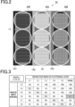
Fig. 2] Fig. 2 is a diagram illustrating a positional relationship between an organic EL device, a color filter, and a microlens in plan view of the display unit. - [
Fig. 3] Fig. 3 is a diagram illustrating a result of ray-trace simulation for a shape of microlenses. - [
Fig. 4] Fig. 4 is a diagram illustrating a result of ray-trace simulation for another shape of microlenses. - [
Fig. 5] Fig. 5 is a diagram illustrating a result of ray-trace simulation for another shape of microlenses. - [
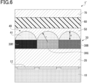
Fig. 6] Fig. 6 is a schematic cross-sectional view illustrating a part of a display unit according to a modification example of an embodiment of the present invention. - Description will be given below of an embodiment of the present invention with reference to
Fig. 1 to Fig. 5 . Adisplay unit 1 according to the present embodiment includesorganic EL devices 11 as light sources and has a configuration in which a large number of pixels are arranged in front view. -
Fig. 1 illustrates a schematic cross-sectional view of a part of thedisplay unit 1 corresponding to one pixel. Thedisplay unit 1 includes adevice substrate 10 on which the organic EL devices (light sources) 11 are disposed and aprotective layer 20, acolor filter 30, alens array 40, and aflattening layer 50, which are formed on thedevice substrate 10. - A
translucent substrate 70 is bonded to theflattening layer 50 via anadhesive layer 60, and a user can see an image displayed by thedisplay unit 1 through thetranslucent substrate 70. - The
organic EL devices 11, which have a known configuration including a pixel electrode, a common electrode, and a functional layer, are connected to non-illustrated wiring provided on thedevice substrate 10 and to be each independently driven for emission. - The
protective layer 20, which is transparent, protects theorganic EL devices 11 and achieves flattening to facilitate the installation of thecolor filter 30. Theprotective layer 20 may be formed of multiple layers and have gas-barrier properties. - A partition may be formed in the
protective layer 20 to define a sub-pixel. The formation of the partition makes it possible to reduce stray light entering adjacent sub-pixels. - The
color filter 30 is provided on the respectiveorganic EL devices 11. Thecolor filter 30 includes a plurality ofmonochromatic filters monochromatic filters organic EL devices 11 in plan view. This is occasionally referred to as the plurality ofmonochromatic filters organic EL devices 11. - The
lens array 40 is formed on thecolor filter 30 and includes a plurality ofmicrolenses 41 arrayed corresponding to the respectivemonochromatic filters color filter 30. Here, the plurality ofmicrolenses 41 being arrayed corresponding to the respectivemonochromatic filters color filter 30 means the plurality ofmicrolenses 41 being arrayed to overlap with the respectivemonochromatic filters color filter 30 in plan view. - The
microlenses 41 according to the present embodiment, which are so-called plano-convex lenses, have refractive indexes higher than at least refractive indexes of air and theflattening layer 50. Here, the plurality ofmicrolenses 41 may be considered to each have the same refractive index. -
Fig. 2 illustrates a positional relationship between theorganic EL devices 11, thecolor filter 30, and themicrolenses 41 in plan view of a range illustrated inFig. 1 . - A pixel of the
display unit 1 includes threesub-pixels monochromatic filter 30R, the greenmonochromatic filter 30G, and the bluemonochromatic filter 30B, which form thecolor filter 30, are disposed for thesub-pixels organic EL devices 11 and three of themicrolenses 41 are disposed for each of thesub-pixels - The above is merely by way of example and a shape of the sub-pixels in plan view and the numbers of
organic EL devices 11 and themicrolenses 41 disposed, and the like may be determined in accordance with the display performance or the like. - The
flattening layer 50 absorbs unevenness of themicrolenses 41 to achieve flattening, which facilitates bonding of thetranslucent substrate 70. Accordingly, a maximum thickness of theflattening layer 50 is equal to or greater than a height of themicrolenses 41. - The
flattening layer 50 has a refractive index lower than the refractive index of themicrolenses 41. The closer the refractive index of theflattening layer 50 is to the refractive index of air, the greater the difference in refractive index between theflattening layer 50 and themicrolenses 41. - The
flattening layer 50 contains, by way of example, a hollow filler and a medium. The hollow filler and the medium are transparent at visible wavelengths and have, for example, a 90% or more total light transmissivity to light at visible wavelengths. The hollow filler contributes to reducing the refractive index of theflattening layer 50. The medium intervenes between particles of the hollow filler to couple the hollow filler particles, which stabilizes theflattening layer 50. - A suitable material of the hollow filler can be exemplified by silicon dioxide (silica, SiO2). A hollow filler including silica is inexpensive and has high transparency to visible wavelengths and physical stability. By virtue of the hollow filler contained in a low-refractive-index layer, air regions are scattered in the
flattening layer 50, resulting in a decrease in the refractive index of theflattening layer 50, and the refractive index approaches a value of that of air with an increase in the content of the hollow filler. - In the
display unit 1, light emitted from the drivenorganic EL devices 11 enters themicrolenses 41 through theprotective layer 20 and thecolor filter 30, and is extracted outside through theflattening layer 50, theadhesive layer 60, and thetranslucent substrate 70. - During the above-described process, light is also refracted at an interface between upper surfaces (lens surfaces) of the
microlenses 41 and theflattening layer 50. Since the refraction varies with a shape of the lens surfaces and the refractive indexes of themicrolenses 41 and theflattening layer 50, the inventor conducted a study regarding optimization thereof to efficiently extract light using a ray-trace simulation. - A model used for the simulation is as follows.
-
- The shape of the microlenses 41: semispherical
- Pitch PD between pixels (gaps): 2.8 µm
- The thickness of the flattening layer 50: 1.2 µm
- Distance DH between the
organic EL device 11 and the microlenses 41: 2.6 µm - The shape of the
microlenses 41 -
Shape 1
Height H: 1.1 µm, curvature radius r of the lens surface: 1.4 µm (r/H 1.27) -
Shape 2
Height H: 0.8 µm, curvature radius r of the lens surface: 1.6 µm (r/H 2.0) -
Shape 3
Height H: 0.6 µm, curvature radius r of the lens surface: 1.9 µm (r/H 3.17) - Refractive index of microlenses 41: in increments of 0.1 from 1.3 to 1.8, refractive index of the flattening layer 50: in increments of 0.1 from 1.1 to 1.5, and no flattening layer 50 (the adhesive layer 60 (refractive index 1.7) was disposed on the lens array 40)
- Under the above-described conditions, the refractive index of the
microlenses 41 was changed in increments of 0.1 and a brightness in a front direction of the pixel was calculated. Further, for each ofShapes 1 to 3 of themicrolenses 41, a rate of improvement or a rate of decrease in brightness was calculated with reference to a brightness under the conditions of "the refractive index of themicrolenses 41 being 1.6, no flatteninglayer 50." -
Fig. 3 to Fig. 5 illustrate simulation results ofShapes 1 to 3, respectively. For example,Fig. 3 shows that at the refractive index of theflattening layer 50 of 1.1 and the refractive index of themicrolenses 41 of 1.3, the brightness was improved by 11% relative to the reference brightness.Fig. 3 also shows that at the refractive index of theflattening layer 50 of 1.5 and the refractive index of themicrolenses 41 of 1.3, the brightness decreased by 35% relative to the reference brightness. - While it has been demonstrated that the brightness tends to be improved relative to the reference by reducing the refractive index of the
flattening layer 50 to be lower than the refractive index of themicrolenses 41 irrespective of the shape, totally unexpected findings were obtained that an excessively low refractive index of the flattening layer or an excessively high refractive index of themicrolenses 41 leads to a decrease in effect in improving the brightness, an optimal range of the difference in refractive index therebetween varies with the shape, and the like. - Specifically, it has been found that a value of the difference in refractive index at which the brightness improvement effect is maximized tends to increase with a decrease in the height of the
microlenses 41 and an increase in the curvature radius of the lens surfaces, that is, an increase in the value of r/H. In this study, an optimal difference in refractive index forShape 1 was 0.3, whereas optimal differences in refractive index forShapes - For the display unit, dimensions of the
microlenses 41 are variously changed in accordance with a pixel dimension or the like. Accordingly, the inventor has tried standardizing conditions that provide a favorable brightness improvement effect on the basis of the above-described findings. As a result, it has been discovered that a favorable brightness improvement effect is obtained in a case where an inequality expression (1) below is satisfied.
- In the expression (1), nm denotes the refractive index of the
microlenses 41 and nt denotes the refractive index of theflattening layer 50. - In this study, for
Shape 1 with r/H in a range of 1 or greater and less than 2, a preferred range of the difference in refractive index was 0.2 or greater and 0.5 or less, and more preferably 0.2 or greater and 0.4 or less. ForShape 2 with r/H in a range of 2 or greater and less than 3, a preferred range of the difference in refractive index was 0.3 or greater and 0.6 or less, and more preferably 0.3 or greater and 0.5 or less. ForShape 3 with r/H in a range of 3 or greater, a preferred range of the difference in refractive index was 0.3 or greater, and more preferably 0.6 or greater and 0.8 or less. The respective conditions for the shapes all satisfy the expression (1) above. - In the
display unit 1 according to the present embodiment, the refractive indexes of themicrolenses 41 and theflattening layer 50 and the shape of themicrolenses 41 are set so as to satisfy the expression (1) above on the basis of the above-described findings, which makes it possible to reduce a loss of outputted light even from light sources that are not so high in directionality, such as theorganic EL devices 11, to improve the usage efficiency. As a result, it is possible to efficiently guide light generated from theorganic EL devices 11 to the front of the unit irrespective of the pixel dimension or the like to significantly improve display quality such as brightness. - In the foregoing, an embodiment of the present invention is described in detail but the present invention is not limited to a specific embodiment and include alterations, combinations, and the like of the configurations within a range not departing from the scope of the present invention. Some of the alterations are described by way of example below but any other alternation is also possible. Two or more of the alterations may be combined as appropriate.
- In the display unit according to the present invention, the light sources are not limited to the above-described
organic EL devices 11 and may bemicro LEDs 12 illustrated inFig. 6 or any other light source device.Fig. 6 illustrates a display unit 1' according to a modification example of an embodiment of the present invention.Fig. 6 , in which the same member as that of thedisplay unit 1 according to an embodiment of the present invention is labeled with the same reference numeral, is different fromFig. 1 merely in that theorganic EL devices 11 of thedisplay unit 1 according to an embodiment are replaced by themicro LEDs 12. Such a display unit 1' also produces an effect similar to that of thedisplay unit 1. - The shape of the
microlenses 41 in plan view is not limited to a circular shape described in the above-described embodiment. For example, as a result of adjacent ones of themicrolenses 41 being provided across the entire sub-pixel through a process such as etch-back, themicrolenses 41 may have the same rectangular shape or the like as the sub-pixel in plan view. - The present invention makes it possible to provide a display unit enabling a reduction in loss of outputted light of a micro LED or an organic EL device to improve usage efficiency.
-
- 10
- Device substrate
- 11
- Organic EL device (light source)
- 20
- Protective layer
- 30
- Color filter
- 30R
- Monochromatic filter (red monochromatic filter)
- 30G
- Monochromatic filter (green monochromatic filter)
- 30B
- Monochromatic filter (blue monochromatic filter)
- 41
- Microlens
- 50
- Flattening layer
- 60
- Adhesive layer
- 70
- Translucent substrate
Claims (6)
- A display unit comprising:a device substrate on which a plurality of light sources are disposed;a protective layer provided on the device substrate to cover the plurality of light sources;a color filter provided on the protective layer, the color filter including a plurality of monochromatic filters disposed corresponding to the plurality of light sources;a lens array provided on the color filter, the lens array including a plurality of microlenses disposed corresponding to the plurality of monochromatic filters; anda flattening layer provided on the lens array to cover the plurality of microlenses, the flattening layer having a refractive index lower than a refractive index of the plurality of microlenses, whereinthe refractive index of the plurality of microlenses denoted by nm, the refractive index of the flattening layer denoted by nt, and a ratio r/H between a curvature radius r and a height H of a lens surface of the plurality of microlenses satisfy the following expression (1):

- The display unit according to claim 1, whereinr/H is 1 or greater and less than 2, anda difference between nm and nt is 0.2 or greater and 0.5 or less.
- The display unit according to claim 1, whereinr/H is 2 or greater and less than 3, anda difference between nm and nt is 0.3 or greater and 0.6 or less.
- The display unit according to claim 1, whereinr/H is 3 or greater, anda difference between nm and nt is 0.6 or greater and 0.8 or less.
- A display unit comprising:a device substrate on which a plurality of light sources are disposed;a protective layer provided on the device substrate to cover the plurality of light sources;a color filter provided on the protective layer, the color filter including a plurality of monochromatic filters disposed corresponding to the plurality of light sources;a lens array provided on the color filter, the lens array including a plurality of microlenses disposed corresponding to the plurality of monochromatic filters; anda flattening layer provided on the lens array to cover the plurality of microlenses, the flattening layer having a refractive index lower than a refractive index of the plurality of microlenses, whereina ratio r/H between a curvature radius r and a height H of a lens surface of the plurality of microlenses is 3 or greater, anda difference between a refractive index nm of the plurality of microlenses and a refractive index nt of the flattening layer is 0.3 or greater.
- The display unit according to any one of claims 1 to 5, wherein
the light sources are organic EL devices or micro LEDs.
Applications Claiming Priority (2)
| Application Number | Priority Date | Filing Date | Title |
|---|---|---|---|
| JP2022065160A JP7806598B2 (en) | 2022-04-11 | 2022-04-11 | display device |
| PCT/JP2023/014028 WO2023199807A1 (en) | 2022-04-11 | 2023-04-05 | Display device |
Publications (2)
| Publication Number | Publication Date |
|---|---|
| EP4510114A1 true EP4510114A1 (en) | 2025-02-19 |
| EP4510114A4 EP4510114A4 (en) | 2025-08-27 |
Family
ID=88329646
Family Applications (1)
| Application Number | Title | Priority Date | Filing Date |
|---|---|---|---|
| EP23788226.1A Pending EP4510114A4 (en) | 2022-04-11 | 2023-04-05 | DISPLAY DEVICE |
Country Status (6)
| Country | Link |
|---|---|
| US (1) | US20250031547A1 (en) |
| EP (1) | EP4510114A4 (en) |
| JP (1) | JP7806598B2 (en) |
| KR (1) | KR20240170908A (en) |
| CN (1) | CN118871966A (en) |
| WO (1) | WO2023199807A1 (en) |
Families Citing this family (1)
| Publication number | Priority date | Publication date | Assignee | Title |
|---|---|---|---|---|
| KR20250064955A (en) * | 2023-11-03 | 2025-05-12 | 엘지디스플레이 주식회사 | Display device |
Family Cites Families (13)
| Publication number | Priority date | Publication date | Assignee | Title |
|---|---|---|---|---|
| KR101372031B1 (en) * | 2009-10-15 | 2014-03-07 | 파나소닉 주식회사 | Display panel device, display device, and method for manufacturing display panel device |
| CN102293053B (en) * | 2010-03-31 | 2015-04-15 | 松下电器产业株式会社 | Display panel device and method for manufacturing display panel device |
| KR20120126562A (en) * | 2011-05-12 | 2012-11-21 | 엘지디스플레이 주식회사 | Image display device |
| JP7151616B2 (en) * | 2019-05-09 | 2022-10-12 | セイコーエプソン株式会社 | Display devices and electronic devices |
| JP7486980B2 (en) | 2020-02-28 | 2024-05-20 | キヤノン株式会社 | Light-emitting device, display device, exposure system, and display/imaging device |
| JP7353834B2 (en) * | 2019-07-12 | 2023-10-02 | キヤノン株式会社 | Display devices and display systems |
| CN110875369A (en) * | 2019-11-27 | 2020-03-10 | 京东方科技集团股份有限公司 | Display back plate, display panel, manufacturing method of display panel and display device |
| CN110928017A (en) * | 2019-12-13 | 2020-03-27 | 武汉华星光电技术有限公司 | Display panel |
| KR102262677B1 (en) * | 2019-12-30 | 2021-06-08 | 엘지디스플레이 주식회사 | Display device and touch display device |
| TW202137598A (en) * | 2020-02-26 | 2021-10-01 | 日商索尼半導體解決方案公司 | Light-emitting element and display device, and method for manufacutring display device |
| JP7030893B2 (en) | 2020-05-27 | 2022-03-07 | ニチハ株式会社 | Wall lumber fixture |
| TW202205913A (en) * | 2020-06-25 | 2022-02-01 | 日商索尼半導體解決方案公司 | display device |
| CN111864119B (en) * | 2020-07-31 | 2024-01-19 | 京东方科技集团股份有限公司 | Display devices and near-eye display devices |
-
2022
- 2022-04-11 JP JP2022065160A patent/JP7806598B2/en active Active
-
2023
- 2023-04-05 KR KR1020247030331A patent/KR20240170908A/en active Pending
- 2023-04-05 EP EP23788226.1A patent/EP4510114A4/en active Pending
- 2023-04-05 WO PCT/JP2023/014028 patent/WO2023199807A1/en not_active Ceased
- 2023-04-05 CN CN202380026726.XA patent/CN118871966A/en active Pending
-
2024
- 2024-10-09 US US18/910,480 patent/US20250031547A1/en active Pending
Also Published As
| Publication number | Publication date |
|---|---|
| US20250031547A1 (en) | 2025-01-23 |
| JP7806598B2 (en) | 2026-01-27 |
| EP4510114A4 (en) | 2025-08-27 |
| CN118871966A (en) | 2024-10-29 |
| KR20240170908A (en) | 2024-12-05 |
| WO2023199807A1 (en) | 2023-10-19 |
| JP2023155685A (en) | 2023-10-23 |
Similar Documents
| Publication | Publication Date | Title |
|---|---|---|
| CN107017269B (en) | Image Sensors Including Dichroic Elements | |
| KR102276434B1 (en) | Image sensor including color separation element and image pickup apparatus including the image sensor | |
| CN102376849B (en) | Semiconductor light-emitting apparatus | |
| KR101348565B1 (en) | Backlight unit and liquid display device that contains it | |
| KR101081246B1 (en) | Light emitting apparatus and fabrication method thereof | |
| KR102159166B1 (en) | Color separation device and image sensor including the color separation device | |
| US9356065B2 (en) | Image sensor having improved light utilization efficiency | |
| EP3148187A1 (en) | Image sensor including color separation element and image pickup apparatus including the image sensor | |
| WO2012077815A1 (en) | Phosphor-based display | |
| CN103885242A (en) | Liquid crystal display device with a light guide plate | |
| US20250031547A1 (en) | Display unit | |
| CN106549088A (en) | Light emitting display device | |
| CN220731555U (en) | Micro display chip structure | |
| CN105867024A (en) | BLU (Backlight Unit) and LCD (Liquid Crystal Display) device | |
| EP4418318A1 (en) | Display panel and display device employing same | |
| CN120813156A (en) | Micro light-emitting device and manufacturing method thereof | |
| CN119546131A (en) | An OLED device with improved brightness based on microlenses | |
| CN114724470A (en) | Miniature LED chip array piece and miniature LED display module | |
| TWI864398B (en) | Micro-led display device having optical coupling microstructures | |
| US20260020412A1 (en) | Display apparatus | |
| CN120813155A (en) | Micro light-emitting device and manufacturing method thereof | |
| CN120916567A (en) | Micro light-emitting device and manufacturing method thereof | |
| WO2025225514A1 (en) | Display device and method for manufacturing same |
Legal Events
| Date | Code | Title | Description |
|---|---|---|---|
| STAA | Information on the status of an ep patent application or granted ep patent |
Free format text: STATUS: THE INTERNATIONAL PUBLICATION HAS BEEN MADE |
|
| PUAI | Public reference made under article 153(3) epc to a published international application that has entered the european phase |
Free format text: ORIGINAL CODE: 0009012 |
|
| STAA | Information on the status of an ep patent application or granted ep patent |
Free format text: STATUS: REQUEST FOR EXAMINATION WAS MADE |
|
| 17P | Request for examination filed |
Effective date: 20240911 |
|
| AK | Designated contracting states |
Kind code of ref document: A1 Designated state(s): AL AT BE BG CH CY CZ DE DK EE ES FI FR GB GR HR HU IE IS IT LI LT LU LV MC ME MK MT NL NO PL PT RO RS SE SI SK SM TR |
|
| DAV | Request for validation of the european patent (deleted) | ||
| DAX | Request for extension of the european patent (deleted) | ||
| REG | Reference to a national code |
Ref country code: DE Ref legal event code: R079 Free format text: PREVIOUS MAIN CLASS: G09F0009300000 Ipc: H10K0050858000 |
|
| A4 | Supplementary search report drawn up and despatched |
Effective date: 20250724 |
|
| RIC1 | Information provided on ipc code assigned before grant |
Ipc: H10K 50/858 20230101AFI20250718BHEP Ipc: H10K 59/38 20230101ALI20250718BHEP Ipc: H10K 59/80 20230101ALI20250718BHEP Ipc: G09F 9/30 20060101ALI20250718BHEP Ipc: G02B 3/00 20060101ALI20250718BHEP Ipc: G02B 5/20 20060101ALI20250718BHEP Ipc: H05B 33/02 20060101ALI20250718BHEP |