EP4507147A1 - Power protection system - Google Patents
Power protection system Download PDFInfo
- Publication number
- EP4507147A1 EP4507147A1 EP24178791.0A EP24178791A EP4507147A1 EP 4507147 A1 EP4507147 A1 EP 4507147A1 EP 24178791 A EP24178791 A EP 24178791A EP 4507147 A1 EP4507147 A1 EP 4507147A1
- Authority
- EP
- European Patent Office
- Prior art keywords
- load
- power
- voltage rail
- side voltage
- capacitor
- Prior art date
- Legal status (The legal status is an assumption and is not a legal conclusion. Google has not performed a legal analysis and makes no representation as to the accuracy of the status listed.)
- Granted
Links
Images




Classifications
-
- H—ELECTRICITY
- H02—GENERATION; CONVERSION OR DISTRIBUTION OF ELECTRIC POWER
- H02H—EMERGENCY PROTECTIVE CIRCUIT ARRANGEMENTS
- H02H3/00—Emergency protective circuit arrangements for automatic disconnection directly responsive to an undesired change from normal electric working condition with or without subsequent reconnection ; integrated protection
- H02H3/02—Details
- H02H3/05—Details with means for increasing reliability, e.g. redundancy arrangements
-
- H—ELECTRICITY
- H02—GENERATION; CONVERSION OR DISTRIBUTION OF ELECTRIC POWER
- H02H—EMERGENCY PROTECTIVE CIRCUIT ARRANGEMENTS
- H02H3/00—Emergency protective circuit arrangements for automatic disconnection directly responsive to an undesired change from normal electric working condition with or without subsequent reconnection ; integrated protection
- H02H3/26—Emergency protective circuit arrangements for automatic disconnection directly responsive to an undesired change from normal electric working condition with or without subsequent reconnection ; integrated protection responsive to difference between voltages or between currents; responsive to phase angle between voltages or between currents
-
- H—ELECTRICITY
- H02—GENERATION; CONVERSION OR DISTRIBUTION OF ELECTRIC POWER
- H02H—EMERGENCY PROTECTIVE CIRCUIT ARRANGEMENTS
- H02H1/00—Details of emergency protective circuit arrangements
- H02H1/0007—Details of emergency protective circuit arrangements concerning the detecting means
-
- H—ELECTRICITY
- H02—GENERATION; CONVERSION OR DISTRIBUTION OF ELECTRIC POWER
- H02H—EMERGENCY PROTECTIVE CIRCUIT ARRANGEMENTS
- H02H3/00—Emergency protective circuit arrangements for automatic disconnection directly responsive to an undesired change from normal electric working condition with or without subsequent reconnection ; integrated protection
- H02H3/44—Emergency protective circuit arrangements for automatic disconnection directly responsive to an undesired change from normal electric working condition with or without subsequent reconnection ; integrated protection responsive to the rate of change of electrical quantities
- H02H3/445—Emergency protective circuit arrangements for automatic disconnection directly responsive to an undesired change from normal electric working condition with or without subsequent reconnection ; integrated protection responsive to the rate of change of electrical quantities of DC quantities
-
- H—ELECTRICITY
- H02—GENERATION; CONVERSION OR DISTRIBUTION OF ELECTRIC POWER
- H02H—EMERGENCY PROTECTIVE CIRCUIT ARRANGEMENTS
- H02H7/00—Emergency protective circuit arrangements specially adapted for specific types of electric machines or apparatus or for sectionalised protection of cable or line systems, and effecting automatic switching in the event of an undesired change from normal working conditions
- H02H7/26—Sectionalised protection of cable or line systems, e.g. for disconnecting a section on which a short-circuit, earth fault, or arc discharge has occured
- H02H7/268—Sectionalised protection of cable or line systems, e.g. for disconnecting a section on which a short-circuit, earth fault, or arc discharge has occured for DC systems
-
- H—ELECTRICITY
- H01—ELECTRIC ELEMENTS
- H01H—ELECTRIC SWITCHES; RELAYS; SELECTORS; EMERGENCY PROTECTIVE DEVICES
- H01H9/00—Details of switching devices, not covered by groups H01H1/00 - H01H7/00
- H01H9/54—Circuit arrangements not adapted to a particular application of the switching device and for which no provision exists elsewhere
- H01H9/548—Electromechanical and static switch connected in series
-
- H—ELECTRICITY
- H02—GENERATION; CONVERSION OR DISTRIBUTION OF ELECTRIC POWER
- H02H—EMERGENCY PROTECTIVE CIRCUIT ARRANGEMENTS
- H02H3/00—Emergency protective circuit arrangements for automatic disconnection directly responsive to an undesired change from normal electric working condition with or without subsequent reconnection ; integrated protection
- H02H3/02—Details
- H02H3/025—Disconnection after limiting, e.g. when limiting is not sufficient or for facilitating disconnection
-
- H—ELECTRICITY
- H02—GENERATION; CONVERSION OR DISTRIBUTION OF ELECTRIC POWER
- H02H—EMERGENCY PROTECTIVE CIRCUIT ARRANGEMENTS
- H02H3/00—Emergency protective circuit arrangements for automatic disconnection directly responsive to an undesired change from normal electric working condition with or without subsequent reconnection ; integrated protection
- H02H3/08—Emergency protective circuit arrangements for automatic disconnection directly responsive to an undesired change from normal electric working condition with or without subsequent reconnection ; integrated protection responsive to excess current
- H02H3/087—Emergency protective circuit arrangements for automatic disconnection directly responsive to an undesired change from normal electric working condition with or without subsequent reconnection ; integrated protection responsive to excess current for DC applications
Definitions
- the present disclosure relates a power protection system, in particular for aerospace DC power systems protection.
- Solid State Circuit Breakers SSCB
- a system has multiple energy sources such as multiple batteries or a mixture of batteries and fuel cells or turbogenerator systems, and multiple loads such as electric propulsion units and pumps. Multiple loads and sources may be connected to a DC distribution system.
- SSCBs use semiconductor devices to interrupt DC currents in case of a fault such as a short-circuit, show a fast response time, and have a high reliability, such that they are preferred over electro-mechanical circuit breakers.
- a power protection system comprising a first DC power source having a positive terminal and a negative terminal, a first load, and a first power bus connecting the first power source and the first load, wherein the first power bus comprises a high side voltage rail connected to the positive terminal and a low side voltage rail connected to the negative terminal.
- the system further comprises a first solid state circuit breaker circuit integrated in the first power bus, wherein the solid state circuit breaker circuit is located at a power source side or at a load side of the first power bus.
- the solid state circuit breaker comprises a first semiconductor switch arranged in the high side voltage rail or in the low side voltage rail and controlled by a control unit, a first capacitor arranged between the high side voltage rail and the low side voltage rail, and a first inductor in one of the high side voltage rail and the low side voltage rail.
- the first capacitor is arranged between the high side voltage rail and the low side voltage rail such that it is located closer to the power source or to the load than the semiconductor switch, wherein a terminal of the first capacitor is arranged between the first semiconductor switch and the power source or between the first semiconductor switch and the load.
- the first inductor is located such that current generated by the first capacitor when unloading in case of a short circuit at the power source or at the load passes the first inductor.
- control unit is configured to measure a voltage change over the first inductor and trigger an actuation signal for the first semiconductor switch if a voltage change over the first inductor surpasses a predetermined threshold voltage.
- aspects of the present disclosure are thus based on the idea of strategically placing an additional (first) capacitor and (first) inductor as close as possible to the load or to the source, wherein in case of a short-circuit the capacitor unloads through the short-circuited load/source and the inductor, thereby causing a boosting current and voltage rise in the inductor that can be detected and used for triggering shutting the SSCB off.
- the additional capacitor provides the least resistance path, it will discharge very quickly, thereby providing the boosting current to the measuring inductor. This way, the present invention increases the quality of fault detection and allows faster clearance of a fault.
- the capacitance of the additional capacitor depends on the circuit conditions but it can be said to be generally small compared to a load capacitance included in the load.
- a small capacitance of the capacitor and its placement in close proximity to the source or load (that may experience a short-circuit) allow ultrafast unloading of the capacitor in case of a short-circuit, thereby providing a boosting current to the inductor that is detected in a short time.
- the capacitance of the capacitor may lie in the range between 1 and 10 ⁇ F.
- a further advantage associated with the present invention lies in that the additional (first) capacitor decouples the main circuit from the short-circuited load/source in microsecond timescale, due to smaller inductance in the conduction path.
- a still further advantage associated with the present invention lies in that significant weight saving compared to the prior art can be achieved where contactors or hybrid breakers are used and as large and bulky inductors to slow a current rise are not required with the present invention.
- the proposed capacitors are light weight and, if film capacitors are used, they are fail-safe.
- a first bypass diode is arranged in parallel to the first capacitor between the high side voltage rail and the low side voltage rail in the blocking direction.
- the diode bypasses the (first) capacitor from charging in the opposite direction that may be caused by higher frequency components such as switching noise and/or harmonics of an inverter representing the load.
- the solid state circuit breaker circuit has a bidirectional conductivity and blocking capability.
- the solid-state circuit breaker circuit may comprise two transistors (such as MOSFET or IGBT) in a row each with antiparallel diodes.
- a bidirectional SSCB may be implemented if the load is with regenerative capability. If using a bidirectional SSCB, such SSCB may be implemented with or without positive and negative breaking capability (meaning that both the high side voltage rail and the low side voltage rail show a bidirectional connectivity and blocking capability versus only one of these shows a bidirectional connectivity and blocking capability).
- Another occasion in which a bidirectional SSCB may be used is if the used power source comprises a high risk of ground fault.
- the solid state circuit breaker circuit has a unidirectional conductivity and blocking capability.
- SSCB may be implemented if the load is with a minimum or no regenerated capability.
- the first semiconductor switch comprises a MOSFET, IGBT, GaN or SiC transistor and a bypass diode in antiparallel to the transistor.
- the semiconductor switch may comprise several of such transistors and bypass diodes (such as in case of a bidirectional SSCB).
- a transient voltage suppressor (TVS) device is arranged in parallel to the semiconductor switch.
- TVS device serves to protect the semiconductor switch by preventing the semiconductor switch from over-voltage stress in a short-circuit condition when a discontinued current flow creates over-voltage which needs to be clamped to a designed voltage level across the TVS device to avoid failure of the semiconductor switch.
- the SSCB trips, the current will be bypassed via the parallel TVS device.
- At least one mechanical contactor is additionally provided that is arranged in series with at least one of the solid state circuit breaker circuits.
- the mechanical contactor allows to provide for galvanic isolation.
- the series connection off a mechanical contactor and an SSCB may be such that the contactor is opened to provide galvanic isolation once a fault has been detected and cleared by the SSCB.
- the first load comprises a capacitive load, wherein the capacitive load is arranged in parallel with the first capacitor, and wherein the capacitive load, the first capacitor and the first inductor form a third order filter.
- a load such as an inverter
- the capacitive load typically includes a capacitive load between the high side voltage rail and the low side voltage rail (the capacitive load also referred to as DC link capacitor).
- the capacitive load buffers energy and filters any AC noise present in the DC line.
- the additional (first) capacitor may have an even smaller capacitance which allows even quicker discharging and boosting the inductor current.
- the controller which controls the semiconductor switch is configured to measure the voltage over the first inductor and to switch the first semiconductor switch off if the measured voltage is larger than the predetermined threshold voltage.
- the voltage across the inductor is equal to dl/dt of the current I. If the current I is increased by a boosted current caused by discharging off the (first) capacitor, the voltage over the inductor surpasses the predetermined threshold voltage.
- SSCB only one SSCB has been considered to be present in a power protection system with one power source and one load.
- two SSCBs are present, one proximate to the power source and one proximate to the load. This allows to independently break the current in case of a fault at the power source side and in case of a fault at the load side.
- the power protection system comprises the first solid state circuit breaker circuit and a second solid state circuit breaker circuit comprising similar components as the first solid state circuit breaker circuit, namely, a second semiconductor switch, a second capacitor and a second inductor, wherein the first solid state circuit breaker circuit is arranged at the power source side and the second solid state circuit breaker circuit is arranged at the load side of the power protection system.
- the power protection system may comprise several power sources and several loads, such that the inventive system is part of such larger power protection system.
- the inventive system may be implemented in some or all parts of a larger power protection system, such as in an SSCB at the power source side of the first power bus, and SSCB at the power source side of a second power bus, and SSCB at the load side of the first power bus, and an SSCB at the load side of the second power bus.
- the power protection system comprises: the first DC power source and a second DC power source, each power source having a positive terminal and a negative terminal; the first load and a second load; the first power bus connecting the first power source and the first load and a second power bus connecting the second power source and the second load, each power bus comprising a high side voltage rail connected to the respective positive terminal and a low side voltage rail connected to the respective negative terminal; the first and second solid state circuit breaker circuits integrated in the first power bus and a third and a fourth solid state circuit breaker circuit integrated into the second power bus (the third and fourth solid state circuit breaker circuits may be configured in the same manner as the first and second solid state circuit breaker circuits); wherein the high side voltage rail of the first power bus and the high side voltage rail of the second power bus are connected and wherein the low side voltage rail of the first power bus and the low side voltage rail of the second power bus are connected.
- the two energy sources may drive one load such as an electric drive if the other load fails, and one energy source may drive to loads if one of the energy sources fails.
- the redundancy may be increased by having additional power sources, loads and connecting power busses.
- This aspect of the present disclosure addresses one main challenge in DC protection, which is, when a short circuit fault happens in any one of the branches of a DC network, all sources and loads see the fault and the DC power busses tend to collapse.
- a further advantage lies in the ability to manage the short circuit fault without collapsing the DC link in a multi SSCB architecture. It is further pointed out that, as each SSCB is controlled by an associated control unit, shutting down of SSCBs is achieved locally, without the requirement of using any communication among different SSCB units, thereby additionally saving time.
- the high side voltage rail of the first power bus and the high side voltage rail of the second power bus are connected in a point in between the respective solid state circuit breaker circuits.
- the low side voltage rail of the first power bus and the low side voltage rail of the second power bus may be connected in a point in between the respective solid state circuit breaker circuits. This way, the connection of the two power buses does not interfere with the SSCBs.
- a middle capacitor wherein the middle capacitor is arranged between the high side voltage rail and the low side voltage rail, wherein the middle capacitor is arranged at a point in between the solid state circuit breaker circuit located at the power source side and the solid state circuit breaker circuit located at the load side.
- the middle capacitor may provide energy to any of the SSCBs.
- the middle capacitor provides additional capability to hold the power bus voltage for a longer time and prevent it from collapsing in case of a short circuit until the fault is cleared.
- the middle capacitor supports the first or any other additional capacitor when providing a booster current to the additional inductor.
- the capacitance of the middle capacitor may lie in the range between 10 and 50 ⁇ F. Generally, the capacitance of the middle capacitor is higher than the capacitance of the additional capacitors.
- each inductor which receives a booster current is associated with a corresponding control unit, the control unit receiving the inductor voltage measurement and providing a gate signals to the semiconductor switch. This allows for quick and decentralized switching of the semiconductor switch in case of a fault without the necessity to communicate among the different breaking units. At the same time, it may be provided that all control units are controlled by a single master controller for communication with a higher level controller.
- the first load and second load may be any load.
- the load may be a power converter such as an inverter.
- the first capacitor is sized such that the capacitance of the first capacitor is smaller than that of the capacitive load, as discussed before.
- Figure 1 shows schematically an electric distribution architecture in which two power sources 21, 22 and two loads R01, R02 are connected through a distribution system. Such system may be used in hybrid propulsion system applications.
- the system of Figure 1 comprises a first power source 21 and a first load R01 connected through a first power bus 31, 41.
- the first power source 21 has a positive terminal 211 and a negative terminal 212. Between these terminals 211, 212 a constant DC voltage such as a battery voltage is present.
- a high side voltage rail 31 is connected to the DC positive terminal 211 and a low side voltage rail 41 is connected to the DC negative terminal 212.
- the high side voltage rail 31 and the low side voltage rail 41 form the first power bus.
- the system further comprises a second power source 22 and a second load R02 connected through a second power bus 32, 42.
- the second power source 22 has a positive terminal 221 and a negative terminal 222. Between these terminals 221, 222 a constant DC voltage such as a battery voltage is present.
- a high side voltage rail 32 is connected to the DC positive terminal 221 and a low side voltage rail 42 is connected to the DC negative terminal 222.
- the high side voltage rail 32 and the low side voltage rail 42 form the second power bus.
- first and second power buses are interconnected.
- the high side voltage rail 31 of the first power bus and the high side voltage rail 32 of the second power bus are connected.
- the low side voltage rail 41 of the first power bus and the low side voltage rail 42 of the second power bus are connected. Accordingly, the same voltage VB+ is present at the high side voltage rails 31, 32, and the same voltage VB- is present at the low side voltage rails 41, 42.
- both power sources 21, 22 can be used to power the remaining load. Further, in case one of the power sources 21, 22 fails, the remaining power source can power both loads R01, R02.
- the power sources 21, 22 may be battery energy storage systems or fuel cells or be fed from a turbo generator/active rectifier.
- the system of Figure 1 further comprises four SSCBs 51-54, wherein SSCB 51 is located at the power source side 61 of the first power bus, SSCB 52 is located at the load side 62 of the first power bus, SSCB 53 is located at the power source side 61 of the second power bus, and SSCB 54 is located at the side 62 of the second power bus.
- the SSCB units 51-54 provide protection function for the respective individual lanes 31, 32, 41, 42 at the power source side 61 and at the load side 62.
- the SSCBs 51-54 are depicted schematically in Figure 1 . They comprise semiconductor switches as will be explained below. Each SSCB 51-54 may comprise semiconductor switches arranged in the high side voltage rail and/or semiconductor switches arranged in the low side voltage rails. In this respect, a plurality of configurations is possible. Depending on the type of source or load, a suitable topology for each of the protection units 51-54 is selected. For example, if the load is with minimum or no regenerative capability, then it is preferred to use unidirectional SSCBs.
- SSCBs with bidirectional protection which may be with positive and negative breaking capability (i.e., semiconductor switches are arranged both on the high side voltage rail and on the low side voltage rail) or without positive and negative breaking capability (i.e., semiconductor switches are arranged on the high side voltage rail or on the low side voltage rail).
- the SSCB should be bidirectional. If the power source is a DC supply like battery or fuel cell, which has a higher risk of ground fault, then it is preferred to adopt SSCBs with bidirectional protection capability and positive and negative lane breaking capability. Selection of the suitable SSCB topology helps to reduce the number of active devices needed to use and reduce the losses on the SSCB.
- the system of Figure 1 further depicts schematically load capacitors C LOAD_1 , C LOAD_2 which represent a capacitive part of the load R01, R02.
- each load R01, R02 in principle, can be any load.
- each load R01, R02 comprises an inverter circuitry.
- Each inverter circuitry may comprise six semiconductor power switches which provide for a three-phase current as is well known to the person skilled in the art.
- Figure 2 shows a first embodiment of a power protection circuit in accordance with aspects of the present invention.
- the general system architecture comprising two power sources 21, 22, two power buses 31, 41, 32, 42 and two loads R01, R02, wherein the power buses are interconnected to provide the same voltage VB+, VB- 1 on the high side voltage rails and the low side voltage rails, reference is made to Figure 1 .
- FIG. 2 shows more details and embodiments of the SSPCs 51-54.
- Each SSPC comprises at least one semiconductor switch, wherein Figure 2 shows three possible configurations of the switching unit of an SSPC.
- the switching unit is bidirectional and located in the high side voltage rail 31. It comprises two switches S10, S11 arranged in a row each comprising a transistor with an antiparallel diode. The antiparallel diodes give current that flows in the opposite direction a path to flow. Without the diodes, inductive currents would cease instantly, generating high voltage peaks.
- SSPC 51 is bidirectional on the high side voltage rail 31.
- the switching unit is unidirectional with one switch S01 comprising a transistor and an antiparallel diode.
- the switching unit is bidirectional on both lanes and comprises two switches S12, S13 on the high side voltage rail 32 and two switches S14, S15 on the low side voltage rail 42, and thus able to isolate both voltage rails 32, 42 in case of a fault.
- SSPC 54 the same configuration is present as in SSPC 52.
- the switches S10, S11, S01, S12-S15, S02 may be MOSFET, GaN (Gallium Nitride), SiC (Silicon Carbide) or IGBT (Insulated Gate Bipolar Transistor) switches. They are controlled by the respective gate voltage, which is provided by a control unit, as discussed with respect to Figure 4 .
- the different configurations of the switching units in Figure 2 are exemplary only.
- the same configuration of the switching unit could be used in all SSPCs 51 to 54, or the configuration may be different (with, e.g., the switching unit of SSBC 52 being bidirectional).
- a small capacitor C10, C01, C11, C02 and a small inductor L10, L01, L11, L02 at the load/source facing terminal are provided.
- capacitor C01 having terminals 101, 102 is arranged between the high side voltage rail 31 and the low side voltage rail 42, wherein capacitor C01 is located as close as possible to the load, which implies that terminal 101 is arranged between the semiconductor switch S01 and the load R01. In case of a short circuit in the load R01, the capacitor C01 unloads through the load R01.
- the inductor L01 is arranged such in the high side voltage rail 31 that current generated by the capacitor C01 when unloading in case of a short circuit passes the inductor L01, thereby creating a boosting current in the inductor L01 that leads to a voltage change over the inductor L01 that is measured and triggers a shutoff signal for the semiconductor switch S01, thereby turning off the load R01.
- the arrangement of the capacitor C01 and of the inductor L01 directly at the load side allows for a very fast fault detection.
- the small capacitor C01 provides the least resistance path, it will discharge very quicky providing the boosting current to the measuring inductor L01.
- the small capacitor C01 decouples the main circuit in microsecond time scales, this being due to device resistance and smaller inductance in the conduction path. The rest of the circuit will see a delayed effect in few microseconds scale giving sufficient time to detect and give an actuation signal to switch S01.
- the capacitance of the capacitors C10, C11, C01, C02 may lie in the range between 10 and 1 and 10 ⁇ F.
- the voltage across the inductor L10, L01, L11, L02 is equal to dl/dt of the current I and hence it will give very fast and clear fault detection compared to other methods.
- capacitor C01 and inductor L01 in SSPC 52 applies similarly to the capacitors C10, C11, C02 and inductors L10, L11, L02 of the other SSPCs 51, 53, 54.
- the distributed capacitors C10, C11, C01, C02 need to be sized to avoid collapsing of the bus voltage and give sufficient delay time to allow fault detection.
- the SSPCs 51-54 further each comprise a diode D10, D01, D11, D02 which is arranged in parallel to the respective capacitor C10, C11, C01, C02.
- the diode D10, D01, D11, D02 is added to provide a continued current path after breaking the switch S10, S11, S01, S12-S15, S02 and bypass the capacitor C10, C11, C01, C02 from charging in the opposite direction.
- the SSPCs 51-54 further comprise a transient voltage suppressor (TVS) device 8.
- TVS transient voltage suppressor
- a TVS device 8 is arranged in parallel to the semiconductor switch S01.
- the TVS device 8 is added to protect the semiconductor switch S01 if an over voltage created by a discontinued current flow in case of a child circuit occurs that needs to be clamped to avoid failure of the semiconductor switches.
- a varistor or snubber circuit or combination of different overvoltage devices can be used.
- Figure 3 shows an embodiment of a power protection system that is similar to the embodiment of Figure 2 , except that in addition a middle capacitor CDC is provided for, to which the voltages VB+, VB- apply.
- the middle capacitor CDC is in addition to the small capacitors C10, C11, C01, C02 and may have a larger capacitance than the small capacitors C10, C11, C01, C02.
- capacitor CDC has more capability to hold the bus voltage for a longer time and prevent it from collapsing in case of a short circuit.
- capacitor CDC supports the capacitors C10, C11, C01, C02 in providing a booster current for the respective inductor L10, L01, L11, L02, which allows the capacitors C10, C11, C01, C02 to be even smaller in capacitance.
- the current from central capacitor CDC in case of a short circuit in the power source/load, while boosting the current through the inductor, is delayed compared to the booster current provided by capacitors C10, C11, C01, C02 because the central capacitor CDC is at a larger distance from the fault condition. Provision of capacitors C10, C11, C01, C02 at the load/power source is thus still relevant for very fast detection of a fault.
- Figure 4 shows a protection circuit/system in accordance with Figure 3 , wherein additional detail about the control system controlling the semiconductor switches is provided for.
- each SSPC 51-54 is associated with a control unit 71-74, wherein the control units 71-74 measure the inductor voltage over the inductors L10, L01, L11, L02 (arrows M1-M4) and provide gate signals (arrow G1-G4) to the respective semiconductor switches. Accordingly, there is local intelligence in the form of the control units 71-74 that decides to switch the respective semiconductor switches S10, S11, S01, S12-S15, S02 off, which saves time.
- the control units 71-74 further receive measurements, error signals and status signals from the switching units (arrows F1-F4).
- Each control unit 71-74 may be incorporated with required gate drivers, measurement and conditioning circuits, protection circuits, etc.
- the required logic circuit for detecting a voltage change over the inductor may be implemented in a hardware circuit in the control units 71-74.
- a multi SSCB controller 75 which provides commands to the individual control units 71-74 (arrows H1-H4) and receives measurements, error signals and status signals the control units 71-74 (arrows J1-J4).
- the multi SSCB controller 75 provides for a higher-level control. It may be implemented in a microprocessor or FPGA which oversees the overall operation and monitors parameters from the different SSCB units.
- the multi SSCB controller 75 may communicate with a higher-level controller (arrow K).
- FIG. 5 shows an example control method that is carried out in control units 71-74 and controller 75.
- each control unit 71-74 it is checked in step 501 if the respective switches are on. This is the normal condition if there is no fault.
- step 502 it is determined whether the voltage VL10, VL11, VL01, VL02 over the respective inductor L10, L11, L02, L02 is larger than a predetermined threshold VL10_MAX, VL11_MAX, VL01_MAX, VL02_MAX. In such case, the respective switches are turned off, step 503.
- step 504. The controller software runs series of checks to confirm whether it is a real fault. If the conditions are acceptable, and/or a fault can be cleared, the respective switches are turned on again, step 505. If not, the respective switches are kept in the OFF state, step 506.
- Steps 501 to 503 may be implemented in the control units 71-74, while steps 504 to 506 may be implemented in the multi SSCB controller 75.
- the proposed topology and method can be adopted in safety critical power distribution systems.
- Figure 6 shows a variant of the embodiment of Figure 3 , wherein the depicted load is an inverter 14 which provides a three-phase current to a motor load 15.
- the SSCB 52 is an integral part of the load side converter 14. This enables to use the capacitor C01 and measuring inductor L01 as part of DC link filter of the inverter 14.
- the load 14 comprises a load capacitor C INV which represents a link filter.
- the link filter buffers energy of the DC link and reduces ripples in the current.
- the additional small capacitors C01 forms together with the load capacitor C INV and the inductor L01 a third order filter 9. Having an additional capacitor C01 significantly reduces the ripple and required size of the DC link capacitor C INV .
- the inverter 14 and the multi SSCBs can be cooled with a common cooling.
- SSPC 54 may be an integral part of a load side converter as well, and SSCB 51 and SSCB 53 may be an integral part of a source side structure.
- Figure 7 shows a further variant of the embodiment of Figure 3 , wherein additionally mechanical contactors CT10, CT01, CT11, CT02 that are connected in series with the SSCBs are provided.
- the mechanical contactors CT10, CT01, CT11, CT02 provide for galvanic isolation in the positive and negative lanes based on protection requirements.
- Such embodiment includes the merits of both SSCBs and contactors: once a fault is cleared by the SSCBs, a contactor CT10, CT01, CT11, CT02 can be used to provide the galvanic isolation. As all protections are in the same housing, they can be controlled with the same control units 71-74 and 75 as discussed with respect to Figure 4 .
Landscapes
- Protection Of Static Devices (AREA)
Abstract
Description
- The present disclosure relates a power protection system, in particular for aerospace DC power systems protection.
- Reliability, availability, and protection are critical to maintain the safety and integrity of aircraft DC power distribution systems. A lack of adequate DC protection devices, poor response times, and an inability to meet aerospace system requirements makes Solid State Circuit Breakers (SSCB) an attractive solution for aerospace DC power distribution and protection. On many occasions a system has multiple energy sources such as multiple batteries or a mixture of batteries and fuel cells or turbogenerator systems, and multiple loads such as electric propulsion units and pumps. Multiple loads and sources may be connected to a DC distribution system.
- SSCBs use semiconductor devices to interrupt DC currents in case of a fault such as a short-circuit, show a fast response time, and have a high reliability, such that they are preferred over electro-mechanical circuit breakers.
- There is a need to stop a fault current, isolate and de-energize the faulted portion of a circuit as fast as possible to minimize the stress on the rest of the system. There is thus a desire for protection systems with very fast fault detection to improve the response time of SSCBs.
- There is a need to provide a power protection system with a Solid State Circuit Breaker which allows for very fast fault detection and a quick response time in case of a fault, or at least provides a useful alternative to known power protection systems.
- In a first aspect there is provided a power protection system. The system comprises a first DC power source having a positive terminal and a negative terminal, a first load, and a first power bus connecting the first power source and the first load, wherein the first power bus comprises a high side voltage rail connected to the positive terminal and a low side voltage rail connected to the negative terminal. The system further comprises a first solid state circuit breaker circuit integrated in the first power bus, wherein the solid state circuit breaker circuit is located at a power source side or at a load side of the first power bus.
- The solid state circuit breaker comprises a first semiconductor switch arranged in the high side voltage rail or in the low side voltage rail and controlled by a control unit, a first capacitor arranged between the high side voltage rail and the low side voltage rail, and a first inductor in one of the high side voltage rail and the low side voltage rail. The first capacitor is arranged between the high side voltage rail and the low side voltage rail such that it is located closer to the power source or to the load than the semiconductor switch, wherein a terminal of the first capacitor is arranged between the first semiconductor switch and the power source or between the first semiconductor switch and the load. The first inductor is located such that current generated by the first capacitor when unloading in case of a short circuit at the power source or at the load passes the first inductor.
- It is further provided that the control unit is configured to measure a voltage change over the first inductor and trigger an actuation signal for the first semiconductor switch if a voltage change over the first inductor surpasses a predetermined threshold voltage.
- Aspects of the present disclosure are thus based on the idea of strategically placing an additional (first) capacitor and (first) inductor as close as possible to the load or to the source, wherein in case of a short-circuit the capacitor unloads through the short-circuited load/source and the inductor, thereby causing a boosting current and voltage rise in the inductor that can be detected and used for triggering shutting the SSCB off. As the additional capacitor provides the least resistance path, it will discharge very quickly, thereby providing the boosting current to the measuring inductor. This way, the present invention increases the quality of fault detection and allows faster clearance of a fault.
- The capacitance of the additional capacitor depends on the circuit conditions but it can be said to be generally small compared to a load capacitance included in the load. A small capacitance of the capacitor and its placement in close proximity to the source or load (that may experience a short-circuit) allow ultrafast unloading of the capacitor in case of a short-circuit, thereby providing a boosting current to the inductor that is detected in a short time. In some embodiments the capacitance of the capacitor may lie in the range between 1 and 10 µF.
- A further advantage associated with the present invention lies in that the additional (first) capacitor decouples the main circuit from the short-circuited load/source in microsecond timescale, due to smaller inductance in the conduction path.
- A still further advantage associated with the present invention lies in that significant weight saving compared to the prior art can be achieved where contactors or hybrid breakers are used and as large and bulky inductors to slow a current rise are not required with the present invention. The proposed capacitors are light weight and, if film capacitors are used, they are fail-safe.
- In some embodiments, a first bypass diode is arranged in parallel to the first capacitor between the high side voltage rail and the low side voltage rail in the blocking direction. The diode bypasses the (first) capacitor from charging in the opposite direction that may be caused by higher frequency components such as switching noise and/or harmonics of an inverter representing the load.
- In some embodiments, the solid state circuit breaker circuit has a bidirectional conductivity and blocking capability. In such case, the solid-state circuit breaker circuit may comprise two transistors (such as MOSFET or IGBT) in a row each with antiparallel diodes. A bidirectional SSCB may be implemented if the load is with regenerative capability. If using a bidirectional SSCB, such SSCB may be implemented with or without positive and negative breaking capability (meaning that both the high side voltage rail and the low side voltage rail show a bidirectional connectivity and blocking capability versus only one of these shows a bidirectional connectivity and blocking capability). Another occasion in which a bidirectional SSCB may be used is if the used power source comprises a high risk of ground fault.
- In some embodiments, the solid state circuit breaker circuit has a unidirectional conductivity and blocking capability. Such SSCB may be implemented if the load is with a minimum or no regenerated capability.
- In some embodiments, the first semiconductor switch comprises a MOSFET, IGBT, GaN or SiC transistor and a bypass diode in antiparallel to the transistor. The semiconductor switch may comprise several of such transistors and bypass diodes (such as in case of a bidirectional SSCB).
- In some embodiments, a transient voltage suppressor (TVS) device is arranged in parallel to the semiconductor switch. Such TVS device serves to protect the semiconductor switch by preventing the semiconductor switch from over-voltage stress in a short-circuit condition when a discontinued current flow creates over-voltage which needs to be clamped to a designed voltage level across the TVS device to avoid failure of the semiconductor switch. When the SSCB trips, the current will be bypassed via the parallel TVS device.
- In some embodiments, at least one mechanical contactor is additionally provided that is arranged in series with at least one of the solid state circuit breaker circuits. The mechanical contactor allows to provide for galvanic isolation. The series connection off a mechanical contactor and an SSCB may be such that the contactor is opened to provide galvanic isolation once a fault has been detected and cleared by the SSCB.
- In some embodiments, the first load comprises a capacitive load, wherein the capacitive load is arranged in parallel with the first capacitor, and wherein the capacitive load, the first capacitor and the first inductor form a third order filter. This embodiment considers the situation that a load (such as an inverter) typically includes a capacitive load between the high side voltage rail and the low side voltage rail (the capacitive load also referred to as DC link capacitor). The capacitive load buffers energy and filters any AC noise present in the DC line. When further considering the capacitive load, the additional (first) capacitor may have an even smaller capacitance which allows even quicker discharging and boosting the inductor current.
- In some embodiments, the controller which controls the semiconductor switch is configured to measure the voltage over the first inductor and to switch the first semiconductor switch off if the measured voltage is larger than the predetermined threshold voltage. In this respect, it is to be noted that the voltage across the inductor is equal to dl/dt of the current I. If the current I is increased by a boosted current caused by discharging off the (first) capacitor, the voltage over the inductor surpasses the predetermined threshold voltage.
- In the above, only one SSCB has been considered to be present in a power protection system with one power source and one load. However, in some embodiments, two SSCBs are present, one proximate to the power source and one proximate to the load. This allows to independently break the current in case of a fault at the power source side and in case of a fault at the load side. In such embodiment, the power protection system comprises the first solid state circuit breaker circuit and a second solid state circuit breaker circuit comprising similar components as the first solid state circuit breaker circuit, namely, a second semiconductor switch, a second capacitor and a second inductor, wherein the first solid state circuit breaker circuit is arranged at the power source side and the second solid state circuit breaker circuit is arranged at the load side of the power protection system.
- Further, in the above, a power protection system with only one power source and only one load has been considered. However, in some embodiments, the power protection system may comprise several power sources and several loads, such that the inventive system is part of such larger power protection system. Also, the inventive system may be implemented in some or all parts of a larger power protection system, such as in an SSCB at the power source side of the first power bus, and SSCB at the power source side of a second power bus, and SSCB at the load side of the first power bus, and an SSCB at the load side of the second power bus.
- In such embodiments, it may be provided that the power protection system comprises: the first DC power source and a second DC power source, each power source having a positive terminal and a negative terminal; the first load and a second load; the first power bus connecting the first power source and the first load and a second power bus connecting the second power source and the second load, each power bus comprising a high side voltage rail connected to the respective positive terminal and a low side voltage rail connected to the respective negative terminal; the first and second solid state circuit breaker circuits integrated in the first power bus and a third and a fourth solid state circuit breaker circuit integrated into the second power bus (the third and fourth solid state circuit breaker circuits may be configured in the same manner as the first and second solid state circuit breaker circuits); wherein the high side voltage rail of the first power bus and the high side voltage rail of the second power bus are connected and wherein the low side voltage rail of the first power bus and the low side voltage rail of the second power bus are connected.
- By the connection of the high side volta ++e rails and the connection of the low side voltage rails of the two power busses, redundancy is provided for: the two energy sources may drive one load such as an electric drive if the other load fails, and one energy source may drive to loads if one of the energy sources fails. The redundancy may be increased by having additional power sources, loads and connecting power busses.
- This aspect of the present disclosure addresses one main challenge in DC protection, which is, when a short circuit fault happens in any one of the branches of a DC network, all sources and loads see the fault and the DC power busses tend to collapse. By providing SSCBs with ultrafast response times in accordance with the present invention in all power busses both at the power source side and at the load side, this problem is solved.
- A further advantage lies in the ability to manage the short circuit fault without collapsing the DC link in a multi SSCB architecture. It is further pointed out that, as each SSCB is controlled by an associated control unit, shutting down of SSCBs is achieved locally, without the requirement of using any communication among different SSCB units, thereby additionally saving time.
- It may be provided that the high side voltage rail of the first power bus and the high side voltage rail of the second power bus are connected in a point in between the respective solid state circuit breaker circuits. Similarly, the low side voltage rail of the first power bus and the low side voltage rail of the second power bus may be connected in a point in between the respective solid state circuit breaker circuits. This way, the connection of the two power buses does not interfere with the SSCBs.
- In some embodiments, there is further provided a middle capacitor, wherein the middle capacitor is arranged between the high side voltage rail and the low side voltage rail, wherein the middle capacitor is arranged at a point in between the solid state circuit breaker circuit located at the power source side and the solid state circuit breaker circuit located at the load side. This way, the middle capacitor may provide energy to any of the SSCBs. The middle capacitor provides additional capability to hold the power bus voltage for a longer time and prevent it from collapsing in case of a short circuit until the fault is cleared. Further, the middle capacitor supports the first or any other additional capacitor when providing a booster current to the additional inductor. In some embodiments the capacitance of the middle capacitor may lie in the range between 10 and 50 µF. Generally, the capacitance of the middle capacitor is higher than the capacitance of the additional capacitors.
- In some embodiments, each inductor which receives a booster current is associated with a corresponding control unit, the control unit receiving the inductor voltage measurement and providing a gate signals to the semiconductor switch. This allows for quick and decentralized switching of the semiconductor switch in case of a fault without the necessity to communicate among the different breaking units. At the same time, it may be provided that all control units are controlled by a single master controller for communication with a higher level controller.
- In principle, the first load and second load may be any load. In some embodiments, the load may be a power converter such as an inverter.
- In case the load comprises a load capacitance, it is provided that the first capacitor is sized such that the capacitance of the first capacitor is smaller than that of the capacitive load, as discussed before.
- The skilled person will appreciate that except where mutually exclusive, a feature or parameter described in relation to any one of the above aspects may be applied to any other aspect. Furthermore, except where mutually exclusive, any feature or parameter described herein may be applied to any aspect and/or combined with any other feature or parameter described herein.
- The power protection system of the present disclosure will be explained in more detail with reference to exemplary embodiments and the accompanying drawings in which:
-
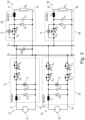
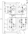
Figure 1 shows an example architecture of a DC distribution system having two power sources and two loads, wherein four schematically depicted SSCB units are provided for power protection, two SSCBs associated with the sources and two SSCBs associated with the loads; -
Figure 2 shows an embodiment of a DC power protection system which may be used in a hybrid propulsion system application, the DC power protection system having a two power sources, two loads and two SSCBs similar toFigure 2 , each SSCB comprising an additional capacitor and an additional inductor for ultrafast detection of a fault at the load side or at the power source side; -
Figure 3 shows the DC power protection system ofFigure 2 , wherein in addition a middle capacitor is provided; -
Figure 4 shows the DC power protection system ofFigure 3 showing additional details about control units controlling the semiconductor switches of the SSCBs; -
Figure 5 is a flowchart of methods that the control units ofFigure 4 employ to determine the presence of a fault; -
Figure 6 shows a DC power protection system similar to the DC power protection system ofFigure 3 , wherein an SSCB is integral part of a load side converter; and -
Figure 7 shows a DC power protection system similar to the DC power protection system ofFigure 3 , wherein in addition mechanical contactors are provided for galvanic isolation. - With increased penetration of electrical systems and the progression towards full electric and hybrid propulsion systems, the use of energy storage system DC power distribution has gained increased use. Protection and distribution network reliability is one of the bottlenecks and proves to be a critical technology in this system. Traditional protection devices, such as fuses and contactors are not suitable due to their response times, their weights, and their dead time. Therefore, there has been increased demand for Solid State Circuit Breakers, SSCBs.
-
Figure 1 shows schematically an electric distribution architecture in which twopower sources - More particularly, the system of
Figure 1 comprises afirst power source 21 and a first load R01 connected through afirst power bus first power source 21 has apositive terminal 211 and anegative terminal 212. Between theseterminals 211, 212 a constant DC voltage such as a battery voltage is present. A highside voltage rail 31 is connected to the DCpositive terminal 211 and a lowside voltage rail 41 is connected to the DCnegative terminal 212. The highside voltage rail 31 and the lowside voltage rail 41 form the first power bus. - In a similar manner, the system further comprises a
second power source 22 and a second load R02 connected through asecond power bus second power source 22 has apositive terminal 221 and anegative terminal 222. Between theseterminals 221, 222 a constant DC voltage such as a battery voltage is present. A highside voltage rail 32 is connected to the DCpositive terminal 221 and a lowside voltage rail 42 is connected to the DCnegative terminal 222. The highside voltage rail 32 and the lowside voltage rail 42 form the second power bus. - Further, the first and second power buses are interconnected. To this end, the high
side voltage rail 31 of the first power bus and the highside voltage rail 32 of the second power bus are connected. Further, the lowside voltage rail 41 of the first power bus and the lowside voltage rail 42 of the second power bus are connected. Accordingly, the same voltage VB+ is present at the high side voltage rails 31, 32, and the same voltage VB- is present at the low side voltage rails 41, 42. In case one of the loads R01, R02 fails, bothpower sources power sources - There may be provided further power sources and loads connected to the system in the same manner.
- In aerospace applications, the
power sources - The system of
Figure 1 further comprises four SSCBs 51-54, whereinSSCB 51 is located at thepower source side 61 of the first power bus,SSCB 52 is located at theload side 62 of the first power bus,SSCB 53 is located at thepower source side 61 of the second power bus, andSSCB 54 is located at theside 62 of the second power bus. The SSCB units 51-54 provide protection function for the respectiveindividual lanes power source side 61 and at theload side 62. - The SSCBs 51-54 are depicted schematically in
Figure 1 . They comprise semiconductor switches as will be explained below. Each SSCB 51-54 may comprise semiconductor switches arranged in the high side voltage rail and/or semiconductor switches arranged in the low side voltage rails. In this respect, a plurality of configurations is possible. Depending on the type of source or load, a suitable topology for each of the protection units 51-54 is selected. For example, if the load is with minimum or no regenerative capability, then it is preferred to use unidirectional SSCBs. If the load is with regenerative capability, then it is preferred to select SSCBs with bidirectional protection, which may be with positive and negative breaking capability (i.e., semiconductor switches are arranged both on the high side voltage rail and on the low side voltage rail) or without positive and negative breaking capability (i.e., semiconductor switches are arranged on the high side voltage rail or on the low side voltage rail). - For example, if the power source is a rectifier extracting power from a turbo generator (such as from a high-pressure shaft, a low-pressure shaft or an intermediate pressure shaft of a gas turbine engine) the SSCB should be bidirectional. If the power source is a DC supply like battery or fuel cell, which has a higher risk of ground fault, then it is preferred to adopt SSCBs with bidirectional protection capability and positive and negative lane breaking capability. Selection of the suitable SSCB topology helps to reduce the number of active devices needed to use and reduce the losses on the SSCB.
- Embodiments of the above-mentioned three types/topologies of an SSCB (unidirectional, bidirectional on one lane, bidirectional on both lanes) are discussed in
Figure 2 . - The system of
Figure 1 further depicts schematically load capacitors CLOAD_1, CLOAD_2 which represent a capacitive part of the load R01, R02. - The loads R01, R02, in principle, can be any load. In embodiments, each load R01, R02 comprises an inverter circuitry. Each inverter circuitry may comprise six semiconductor power switches which provide for a three-phase current as is well known to the person skilled in the art.
- One of the main problems in DC distribution systems is when a fault happens it will be seen by all the connected systems and if there are energy source or capacitors in the power busses, they start contributing to the fault location. This makes it very challenging for reliable fault identification and isolation.
-
Figure 2 shows a first embodiment of a power protection circuit in accordance with aspects of the present invention. As to the general system architecture comprising twopower sources power buses Figure 1 . -
Figure 2 shows more details and embodiments of the SSPCs 51-54. Each SSPC comprises at least one semiconductor switch, whereinFigure 2 shows three possible configurations of the switching unit of an SSPC. InSSPC 51, the switching unit is bidirectional and located in the highside voltage rail 31. It comprises two switches S10, S11 arranged in a row each comprising a transistor with an antiparallel diode. The antiparallel diodes give current that flows in the opposite direction a path to flow. Without the diodes, inductive currents would cease instantly, generating high voltage peaks.SSPC 51 is bidirectional on the highside voltage rail 31. - In
SSPC 52, the switching unit is unidirectional with one switch S01 comprising a transistor and an antiparallel diode. InSSPC 53, the switching unit is bidirectional on both lanes and comprises two switches S12, S13 on the highside voltage rail 32 and two switches S14, S15 on the lowside voltage rail 42, and thus able to isolate bothvoltage rails SSPC 54, the same configuration is present as inSSPC 52. - The switches S10, S11, S01, S12-S15, S02 may be MOSFET, GaN (Gallium Nitride), SiC (Silicon Carbide) or IGBT (Insulated Gate Bipolar Transistor) switches. They are controlled by the respective gate voltage, which is provided by a control unit, as discussed with respect to
Figure 4 . - It is pointed out that the different configurations of the switching units in
Figure 2 are exemplary only. For example, the same configuration of the switching unit could be used in allSSPCs 51 to 54, or the configuration may be different (with, e.g., the switching unit ofSSBC 52 being bidirectional). - In accordance with aspects of the present invention, in each of the SSCBs 51-54, a small capacitor C10, C01, C11, C02 and a small inductor L10, L01, L11, L02 at the load/source facing terminal are provided. For example, when considering
load facing SSPC 52, capacitor C01 having terminals 101, 102 is arranged between the highside voltage rail 31 and the lowside voltage rail 42, wherein capacitor C01 is located as close as possible to the load, which implies that terminal 101 is arranged between the semiconductor switch S01 and the load R01. In case of a short circuit in the load R01, the capacitor C01 unloads through the load R01. The inductor L01 is arranged such in the highside voltage rail 31 that current generated by the capacitor C01 when unloading in case of a short circuit passes the inductor L01, thereby creating a boosting current in the inductor L01 that leads to a voltage change over the inductor L01 that is measured and triggers a shutoff signal for the semiconductor switch S01, thereby turning off the load R01. - The arrangement of the capacitor C01 and of the inductor L01 directly at the load side allows for a very fast fault detection. As the small capacitor C01 provides the least resistance path, it will discharge very quicky providing the boosting current to the measuring inductor L01. Also, the small capacitor C01 decouples the main circuit in microsecond time scales, this being due to device resistance and smaller inductance in the conduction path. The rest of the circuit will see a delayed effect in few microseconds scale giving sufficient time to detect and give an actuation signal to switch S01.
- The capacitance of the capacitors C10, C11, C01, C02 may lie in the range between 10 and 1 and 10 µF.
- The voltage across the inductor L10, L01, L11, L02 is equal to dl/dt of the current I and hence it will give very fast and clear fault detection compared to other methods.
- The above explanation of the function of capacitor C01 and inductor L01 in
SSPC 52 applies similarly to the capacitors C10, C11, C02 and inductors L10, L11, L02 of theother SSPCs - Generally, the distributed capacitors C10, C11, C01, C02 need to be sized to avoid collapsing of the bus voltage and give sufficient delay time to allow fault detection.
- The SSPCs 51-54 further each comprise a diode D10, D01, D11, D02 which is arranged in parallel to the respective capacitor C10, C11, C01, C02. The diode D10, D01, D11, D02 is added to provide a continued current path after breaking the switch S10, S11, S01, S12-S15, S02 and bypass the capacitor C10, C11, C01, C02 from charging in the opposite direction.
- The SSPCs 51-54 further comprise a transient voltage suppressor (TVS)
device 8. For example, inSSPC 52, aTVS device 8 is arranged in parallel to the semiconductor switch S01. TheTVS device 8 is added to protect the semiconductor switch S01 if an over voltage created by a discontinued current flow in case of a child circuit occurs that needs to be clamped to avoid failure of the semiconductor switches. Alternatively to aTVS device 8, a varistor or snubber circuit or combination of different overvoltage devices can be used. - Summarizing, in
Figure 4 fast fault protection is enabled that prevents the system to collapse in case of a short circuit, wherein the bus voltage is not allowed to fall until the faulty branch is cleared from the fault. -
Figure 3 shows an embodiment of a power protection system that is similar to the embodiment ofFigure 2 , except that in addition a middle capacitor CDC is provided for, to which the voltages VB+, VB- apply. The middle capacitor CDC is in addition to the small capacitors C10, C11, C01, C02 and may have a larger capacitance than the small capacitors C10, C11, C01, C02. - One additional advantage of this configuration lies in that capacitor CDC has more capability to hold the bus voltage for a longer time and prevent it from collapsing in case of a short circuit. At the same time, capacitor CDC supports the capacitors C10, C11, C01, C02 in providing a booster current for the respective inductor L10, L01, L11, L02, which allows the capacitors C10, C11, C01, C02 to be even smaller in capacitance. In this respect, it is to be noted that the current from central capacitor CDC in case of a short circuit in the power source/load, while boosting the current through the inductor, is delayed compared to the booster current provided by capacitors C10, C11, C01, C02 because the central capacitor CDC is at a larger distance from the fault condition. Provision of capacitors C10, C11, C01, C02 at the load/power source is thus still relevant for very fast detection of a fault.
-
Figure 4 shows a protection circuit/system in accordance withFigure 3 , wherein additional detail about the control system controlling the semiconductor switches is provided for. - As shown in
Figure 4 , each SSPC 51-54 is associated with a control unit 71-74, wherein the control units 71-74 measure the inductor voltage over the inductors L10, L01, L11, L02 (arrows M1-M4) and provide gate signals (arrow G1-G4) to the respective semiconductor switches. Accordingly, there is local intelligence in the form of the control units 71-74 that decides to switch the respective semiconductor switches S10, S11, S01, S12-S15, S02 off, which saves time. - The control units 71-74 further receive measurements, error signals and status signals from the switching units (arrows F1-F4). Each control unit 71-74 may be incorporated with required gate drivers, measurement and conditioning circuits, protection circuits, etc.
- To further support fast detection of a fault, the required logic circuit for detecting a voltage change over the inductor may be implemented in a hardware circuit in the control units 71-74.
- There is further provided a
multi SSCB controller 75 which provides commands to the individual control units 71-74 (arrows H1-H4) and receives measurements, error signals and status signals the control units 71-74 (arrows J1-J4). Themulti SSCB controller 75 provides for a higher-level control. It may be implemented in a microprocessor or FPGA which oversees the overall operation and monitors parameters from the different SSCB units. Themulti SSCB controller 75 may communicate with a higher-level controller (arrow K). -
Figure 5 shows an example control method that is carried out in control units 71-74 andcontroller 75. In each control unit 71-74, it is checked instep 501 if the respective switches are on. This is the normal condition if there is no fault. Instep 502, it is determined whether the voltage VL10, VL11, VL01, VL02 over the respective inductor L10, L11, L02, L02 is larger than a predetermined threshold VL10_MAX, VL11_MAX, VL01_MAX, VL02_MAX. In such case, the respective switches are turned off,step 503. - In case the switches are turned off, the status and measurements are checked,
step 504. The controller software runs series of checks to confirm whether it is a real fault. If the conditions are acceptable, and/or a fault can be cleared, the respective switches are turned on again,step 505. If not, the respective switches are kept in the OFF state,step 506. -
Steps 501 to 503 may be implemented in the control units 71-74, whilesteps 504 to 506 may be implemented in themulti SSCB controller 75. - The proposed topology and method can be adopted in safety critical power distribution systems.
-
Figure 6 shows a variant of the embodiment ofFigure 3 , wherein the depicted load is aninverter 14 which provides a three-phase current to amotor load 15. In this embodiment, theSSCB 52 is an integral part of theload side converter 14. This enables to use the capacitor C01 and measuring inductor L01 as part of DC link filter of theinverter 14. - More particularly, the
load 14 comprises a load capacitor CINV which represents a link filter. The link filter buffers energy of the DC link and reduces ripples in the current. Here, the additional small capacitors C01 forms together with the load capacitor CINV and the inductor L01 athird order filter 9. Having an additional capacitor C01 significantly reduces the ripple and required size of the DC link capacitor CINV. - Additionally, the
inverter 14 and the multi SSCBs can be cooled with a common cooling. - Similarly,
SSPC 54 may be an integral part of a load side converter as well, andSSCB 51 andSSCB 53 may be an integral part of a source side structure. -
Figure 7 shows a further variant of the embodiment ofFigure 3 , wherein additionally mechanical contactors CT10, CT01, CT11, CT02 that are connected in series with the SSCBs are provided. The mechanical contactors CT10, CT01, CT11, CT02 provide for galvanic isolation in the positive and negative lanes based on protection requirements. - Such embodiment includes the merits of both SSCBs and contactors: once a fault is cleared by the SSCBs, a contactor CT10, CT01, CT11, CT02 can be used to provide the galvanic isolation. As all protections are in the same housing, they can be controlled with the same control units 71-74 and 75 as discussed with respect to
Figure 4 . - It should be understood that the above description is intended for illustrative purposes only, and is not intended to limit the scope of the present disclosure in any way. Also, those skilled in the art will appreciate that other aspects of the disclosure can be obtained from a study of the drawings, the disclosure and the appended claims. All methods described herein can be performed in any suitable order unless otherwise indicated herein or otherwise clearly contradicted by context. Various features of the various embodiments disclosed herein can be combined in different combinations to create new embodiments within the scope of the present disclosure. In particular, the disclosure extends to and includes all combinations and sub-combinations of one or more features described herein. Any ranges given herein include any and all specific values within the range and any and all sub-ranges within the given range.
Claims (15)
- A power protection system comprising:a first DC power source (21) having a positive terminal (211) and a negative terminal (212);a first load (R01);a first power bus (31, 41) connecting the first power source (21) and the first load (R01);the first power bus (31, 41) comprising a high side voltage rail (31) connected to the positive terminal (211) and a low side voltage rail (41) connected to the negative terminal (212);a first solid state circuit breaker circuit (51, 52) integrated in the first power bus (31, 41), the first solid state circuit breaker circuit (51, 52) located at a power source side (61) or at a load side (62) of the first power bus (31, 41), the first solid state circuit breaker (51, 52) comprising:a first semiconductor switch (S10, S11; S01) arranged in the high side voltage rail (31) or in the low side voltage rail (41) and controlled by a control unit (71, 72);a first capacitor (C10, C01) arranged between the high side voltage rail (31) and the low side voltage rail (41), wherein the first capacitor (C10, C01) is arranged between the high side voltage rail (31) and the low side voltage rail (41) closer to the power source (21) or to the load (R01) than the semiconductor switch (S10, S11; S01), and wherein a terminal (101) of the first capacitor (C10, C01) is arranged between the first semiconductor switch (S10, S11) and the power source (21) or between the first semiconductor switch (S01) and the load (R01); anda first inductor (L10, L01) in one of the high side voltage rail (31) and the low side voltage rail (41), wherein the first inductor (L10, L01) is located such that current generated by the first capacitor (C10, C01) when unloading in case of a short circuit at the power source (21) or at the load (R01) passes the first inductor (L10, L01);wherein the control unit (71, 72) is configured to measure a voltage change over the first inductor (L10, L01) and trigger an actuation signal for the first semiconductor switch (S10, S11; S01) if a voltage change over the first inductor (L10, L01) surpasses a predetermined threshold voltage (VL10_MAX, VL11_MAX, VL01_MAX, VL02_MAX).
- The power protection system of claim 1, wherein a first bypass diode (D10, D01) is arranged in parallel to the first capacitor (C10, C01) between the high side voltage rail (31) and the low side voltage rail (41) in the blocking direction.
- The power protection system of claim 1 or 2, wherein the solid state circuit breaker circuit (51, 52) has a bidirectional conductivity and blocking capability.
- The power protection system of claim 1 or 2, wherein the solid state circuit breaker circuit (51, 52) has a unidirectional conductivity and blocking capability.
- The power protection system of any preceding claim, wherein the first semiconductor switch (S10, S11; S01) comprises a MOSFET, IGBT, GaN or SiC transistor and a bypass diode in antiparallel to the transistor (T).
- The power protection system of any preceding claim, wherein a transient voltage suppressor device (8) is arranged in parallel to the semiconductor switch (S01).
- The power protection system of any preceding claim, wherein at least one mechanical contactor (CT10, CT01) that is arranged in series with at least one of the solid state circuit breaker circuits (51, 52).
- The power protection system of any preceding claim, wherein the first load (R01) comprises a capacitive load (CINV), the capacitive load (CINV) being arranged in parallel with the first capacitor (C01), wherein the capacitive load (CINV), the first capacitor (C01) and the first inductor (L01) form a third order filter (9).
- The power protection system of any preceding claim, wherein the controller (71, 72) is configured to constantly measure the voltage over the first inductor (L10, L01), and to turn the first semiconductor switch off (S10, S11; S01) if the measured voltage is larger than the predetermined threshold voltage
- The power protection system of any preceding claim, wherein the power protection system comprises the first solid state circuit breaker circuit (51) and a second solid state circuit breaker circuit (52) comprising similar components as the first solid state circuit breaker circuit (51), namely, a second semiconductor switch (S01), a second capacitor (C01) and a second inductor (L01), wherein the first solid state circuit breaker circuit (51) is arranged at the power source side (61) and the second solid state circuit breaker circuit (52) is arranged at the load side (62) of the power protection system.
- The power protection system of claim 10, wherein the power protection system comprises:the first DC power source (21) and a second DC power source (22), each power source having a positive terminal (211, 212) and a negative terminal (221, 222);the first load (R01) and a second load (R02);the first power bus (31, 41) connecting the first power source (21) and the first load (R01) and a second power bus (32, 42) connecting the second power source (22) and the second load (R02), each power bus (31, 41; 32, 42) comprising a high side voltage rail (31, 41) connected to the respective positive terminal (211, 221) and a low side voltage rail (41, 42) connected to the respective negative terminal (212, 222); andthe first and second solid state circuit breaker circuits (51, 52) integrated in the first power bus (31, 41) and a third and a fourth solid state circuit breaker circuit (53, 54) integrated into the second power bus (32, 42);wherein the high side voltage rail (31) of the first power bus and the high side voltage rail (32) of the second power bus are connected and wherein the low side voltage rail (41) of the first power bus and the low side voltage rail (42) of the second power bus are connected.
- The power protection system of claim 11, wherein a middle capacitor (CDC) is provided, the middle capacitor (CDC) arranged between the high side voltage rail (31, 41) and the low side voltage rail (32, 42), wherein the middle capacitor (CDC) is arranged at a point in between the solid state circuit breaker circuit (51, 53) located at the power source side (61) and the solid state circuit breaker circuit (52, 54) located at the load side (62).
- The power protection system of claim 11 or 12, wherein each inductor (L10, L01, L11, L02) is associated with a corresponding control unit (71-74), each control unit (71-74) receiving the inductor voltage measurement and providing a gate signal to the semiconductor switch (S10, S11; S01; S12-S14; S02).
- The power protection system of any preceding claim, wherein the first load (R01) is an inverter (14).
- The power protection system of any preceding claim, wherein the first capacitor (C10, C01) is sized such that the capacitance of the first capacitor (C10, C01) is smaller than the capacitance of a capacitive load (CINV).
Applications Claiming Priority (1)
| Application Number | Priority Date | Filing Date | Title |
|---|---|---|---|
| GBGB2310964.8A GB202310964D0 (en) | 2023-07-18 | 2023-07-18 | Power protection system |
Publications (2)
| Publication Number | Publication Date |
|---|---|
| EP4507147A1 true EP4507147A1 (en) | 2025-02-12 |
| EP4507147B1 EP4507147B1 (en) | 2026-04-15 |
Family
ID=87758407
Family Applications (1)
| Application Number | Title | Priority Date | Filing Date |
|---|---|---|---|
| EP24178791.0A Active EP4507147B1 (en) | 2023-07-18 | 2024-05-29 | Power protection system |
Country Status (3)
| Country | Link |
|---|---|
| US (1) | US20250030234A1 (en) |
| EP (1) | EP4507147B1 (en) |
| GB (1) | GB202310964D0 (en) |
Families Citing this family (1)
| Publication number | Priority date | Publication date | Assignee | Title |
|---|---|---|---|---|
| CN120110006B (en) * | 2025-02-28 | 2026-05-12 | 北京航天时代微机电技术有限公司 | High-power anti-reverse power distribution control and detection circuit and method |
Citations (2)
| Publication number | Priority date | Publication date | Assignee | Title |
|---|---|---|---|---|
| US20170104327A1 (en) * | 2015-10-12 | 2017-04-13 | Eaton Corporation | Semiconductor circuit interruption devices using current filtering to improve device coordination |
| EP3754346A1 (en) * | 2019-06-17 | 2020-12-23 | Lisa Dräxlmaier GmbH | Detection device, switching device, power supply system, detection method and method |
Family Cites Families (3)
| Publication number | Priority date | Publication date | Assignee | Title |
|---|---|---|---|---|
| US8779735B2 (en) * | 2011-03-15 | 2014-07-15 | Infineon Technologies Ag | System and method for an overcurrent protection and interface circuit between an energy source and a load |
| US20140029152A1 (en) * | 2012-03-30 | 2014-01-30 | Semisouth Laboratories, Inc. | Solid-state circuit breakers |
| US8958193B2 (en) * | 2013-03-15 | 2015-02-17 | Northrop Grumman Systems Corporation | System and method for providing optically triggered circuit breaker |
-
2023
- 2023-07-18 GB GBGB2310964.8A patent/GB202310964D0/en not_active Ceased
-
2024
- 2024-05-29 EP EP24178791.0A patent/EP4507147B1/en active Active
- 2024-06-10 US US18/738,641 patent/US20250030234A1/en active Pending
Patent Citations (2)
| Publication number | Priority date | Publication date | Assignee | Title |
|---|---|---|---|---|
| US20170104327A1 (en) * | 2015-10-12 | 2017-04-13 | Eaton Corporation | Semiconductor circuit interruption devices using current filtering to improve device coordination |
| EP3754346A1 (en) * | 2019-06-17 | 2020-12-23 | Lisa Dräxlmaier GmbH | Detection device, switching device, power supply system, detection method and method |
Also Published As
| Publication number | Publication date |
|---|---|
| EP4507147B1 (en) | 2026-04-15 |
| US20250030234A1 (en) | 2025-01-23 |
| GB202310964D0 (en) | 2023-08-30 |
Similar Documents
| Publication | Publication Date | Title |
|---|---|---|
| JP7807204B2 (en) | A smart battery disconnect protection architecture for airborne high-power modular multi-string battery packs | |
| US9735573B2 (en) | DC-power system with system protection capabilities | |
| EP3872944A1 (en) | Direct current energy dissipation apparatus and control method therefor | |
| US8624437B2 (en) | Power conversion system and method | |
| EP3051646B1 (en) | Direct current power system | |
| EP3096435B1 (en) | Uninterruptable power supply system with fault clear capability | |
| EP3910771B1 (en) | Dc bus precharge system | |
| CA2620100A1 (en) | Inverter circuit with distributed energy stores | |
| CN1139307A (en) | Power Converter Protection Devices for Power Systems | |
| CN112640238B (en) | Method and device for identifying a fault in an HVDC line and generating a trigger signal for a DC circuit breaker | |
| KR101175576B1 (en) | Static energising system for a generator and method for operation of such an energising system | |
| EP3379674A1 (en) | Power distribution system | |
| CN110192343A (en) | Power supply system and method | |
| EP4507147B1 (en) | Power protection system | |
| WO2021005793A1 (en) | Dc distribution panel | |
| JP2004112929A (en) | Ac-dc converter | |
| Gleissner et al. | A real-life fuse design for a fault-tolerant motor inverter | |
| Sztykiel et al. | AC/DC converter with DC fault suppression for aircraft+/− 270 VDC distribution systems | |
| EP4020731A1 (en) | Fault clearing in midpoint grounded systems | |
| US20250226760A1 (en) | Electrical power system | |
| Peng et al. | Fault Tolerant More Electric Engine/Aircraft Architecture with Integrated Condition-Based Control | |
| CN121307789B (en) | Full-link fault isolation control method and device for eVTOL low-voltage distribution box | |
| Yang et al. | Current-limiting and Short-circuit Protection for Shipboard AC Smart Power Distribution Module in Centralized Power System | |
| WO2025061356A1 (en) | Dc power distribution and protection system | |
| US12388293B2 (en) | Hybrid bridge transfer switch system and methods |
Legal Events
| Date | Code | Title | Description |
|---|---|---|---|
| PUAI | Public reference made under article 153(3) epc to a published international application that has entered the european phase |
Free format text: ORIGINAL CODE: 0009012 |
|
| STAA | Information on the status of an ep patent application or granted ep patent |
Free format text: STATUS: THE APPLICATION HAS BEEN PUBLISHED |
|
| AK | Designated contracting states |
Kind code of ref document: A1 Designated state(s): AL AT BE BG CH CY CZ DE DK EE ES FI FR GB GR HR HU IE IS IT LI LT LU LV MC ME MK MT NL NO PL PT RO RS SE SI SK SM TR |
|
| STAA | Information on the status of an ep patent application or granted ep patent |
Free format text: STATUS: REQUEST FOR EXAMINATION WAS MADE |
|
| 17P | Request for examination filed |
Effective date: 20250730 |
|
| GRAP | Despatch of communication of intention to grant a patent |
Free format text: ORIGINAL CODE: EPIDOSNIGR1 |
|
| STAA | Information on the status of an ep patent application or granted ep patent |
Free format text: STATUS: GRANT OF PATENT IS INTENDED |
|
| RIC1 | Information provided on ipc code assigned before grant |
Ipc: H02H 3/05 20060101AFI20251103BHEP Ipc: H02H 3/44 20060101ALI20251103BHEP Ipc: H02H 7/26 20060101ALI20251103BHEP Ipc: H01H 9/54 20060101ALN20251103BHEP Ipc: H02H 3/02 20060101ALN20251103BHEP Ipc: H02H 3/087 20060101ALN20251103BHEP |
|
| INTG | Intention to grant announced |
Effective date: 20251121 |
|
| GRAS | Grant fee paid |
Free format text: ORIGINAL CODE: EPIDOSNIGR3 |
|
| GRAA | (expected) grant |
Free format text: ORIGINAL CODE: 0009210 |
|
| STAA | Information on the status of an ep patent application or granted ep patent |
Free format text: STATUS: THE PATENT HAS BEEN GRANTED |
|
| AK | Designated contracting states |
Kind code of ref document: B1 Designated state(s): AL AT BE BG CH CY CZ DE DK EE ES FI FR GB GR HR HU IE IS IT LI LT LU LV MC ME MK MT NL NO PL PT RO RS SE SI SK SM TR |
|
| REG | Reference to a national code |
Ref country code: CH Ref legal event code: F10 Free format text: ST27 STATUS EVENT CODE: U-0-0-F10-F00 (AS PROVIDED BY THE NATIONAL OFFICE) Effective date: 20260415 |
|
| P01 | Opt-out of the competence of the unified patent court (upc) registered |
Free format text: CASE NUMBER: UPC_APP_0011742_4507147/2026 Effective date: 20260401 |
|
| REG | Reference to a national code |
Ref country code: DE Ref legal event code: R096 Ref document number: 602024003916 Country of ref document: DE |