EP4507120A1 - Antenna-in-package construction with frequency division duplex technology - Google Patents
Antenna-in-package construction with frequency division duplex technology Download PDFInfo
- Publication number
- EP4507120A1 EP4507120A1 EP23203470.2A EP23203470A EP4507120A1 EP 4507120 A1 EP4507120 A1 EP 4507120A1 EP 23203470 A EP23203470 A EP 23203470A EP 4507120 A1 EP4507120 A1 EP 4507120A1
- Authority
- EP
- European Patent Office
- Prior art keywords
- antenna
- antennas
- chip
- package construction
- dielectric layer
- Prior art date
- Legal status (The legal status is an assumption and is not a legal conclusion. Google has not performed a legal analysis and makes no representation as to the accuracy of the status listed.)
- Granted
Links
Images




Classifications
-
- H—ELECTRICITY
- H01—ELECTRIC ELEMENTS
- H01Q—ANTENNAS, i.e. RADIO AERIALS
- H01Q21/00—Antenna arrays or systems
- H01Q21/06—Arrays of individually energised antenna units similarly polarised and spaced apart
- H01Q21/061—Two dimensional planar arrays
- H01Q21/065—Patch antenna array
-
- H—ELECTRICITY
- H01—ELECTRIC ELEMENTS
- H01Q—ANTENNAS, i.e. RADIO AERIALS
- H01Q1/00—Details of, or arrangements associated with, antennas
- H01Q1/12—Supports; Mounting means
- H01Q1/22—Supports; Mounting means by structural association with other equipment or articles
- H01Q1/2283—Supports; Mounting means by structural association with other equipment or articles mounted in or on the surface of a semiconductor substrate as a chip-type antenna or integrated with other components into an IC package
-
- H—ELECTRICITY
- H01—ELECTRIC ELEMENTS
- H01Q—ANTENNAS, i.e. RADIO AERIALS
- H01Q1/00—Details of, or arrangements associated with, antennas
- H01Q1/52—Means for reducing coupling between antennas; Means for reducing coupling between an antenna and another structure
- H01Q1/521—Means for reducing coupling between antennas; Means for reducing coupling between an antenna and another structure reducing the coupling between adjacent antennas
- H01Q1/523—Means for reducing coupling between antennas; Means for reducing coupling between an antenna and another structure reducing the coupling between adjacent antennas between antennas of an array
-
- H—ELECTRICITY
- H01—ELECTRIC ELEMENTS
- H01Q—ANTENNAS, i.e. RADIO AERIALS
- H01Q1/00—Details of, or arrangements associated with, antennas
- H01Q1/52—Means for reducing coupling between antennas; Means for reducing coupling between an antenna and another structure
- H01Q1/521—Means for reducing coupling between antennas; Means for reducing coupling between an antenna and another structure reducing the coupling between adjacent antennas
- H01Q1/525—Means for reducing coupling between antennas; Means for reducing coupling between an antenna and another structure reducing the coupling between adjacent antennas between emitting and receiving antennas
-
- H—ELECTRICITY
- H01—ELECTRIC ELEMENTS
- H01Q—ANTENNAS, i.e. RADIO AERIALS
- H01Q1/00—Details of, or arrangements associated with, antennas
- H01Q1/52—Means for reducing coupling between antennas; Means for reducing coupling between an antenna and another structure
- H01Q1/526—Electromagnetic shields
-
- H—ELECTRICITY
- H01—ELECTRIC ELEMENTS
- H01Q—ANTENNAS, i.e. RADIO AERIALS
- H01Q5/00—Arrangements for simultaneous operation of antennas on two or more different wavebands, e.g. dual-band or multi-band arrangements
- H01Q5/40—Imbricated or interleaved structures; Combined or electromagnetically coupled arrangements, e.g. comprising two or more non-connected fed radiating elements
- H01Q5/42—Imbricated or interleaved structures; Combined or electromagnetically coupled arrangements, e.g. comprising two or more non-connected fed radiating elements using two or more imbricated arrays
-
- H—ELECTRICITY
- H10—SEMICONDUCTOR DEVICES; ELECTRIC SOLID-STATE DEVICES NOT OTHERWISE PROVIDED FOR
- H10W—GENERIC PACKAGES, INTERCONNECTIONS, CONNECTORS OR OTHER CONSTRUCTIONAL DETAILS OF DEVICES COVERED BY CLASS H10
- H10W42/00—Arrangements for protection of devices
- H10W42/20—Arrangements for protection of devices protecting against electromagnetic or particle radiation, e.g. light, X-rays, gamma-rays or electrons
- H10W42/261—Arrangements for protection of devices protecting against electromagnetic or particle radiation, e.g. light, X-rays, gamma-rays or electrons characterised by their shapes or dispositions
- H10W42/263—Shielding bumps
-
- H—ELECTRICITY
- H10—SEMICONDUCTOR DEVICES; ELECTRIC SOLID-STATE DEVICES NOT OTHERWISE PROVIDED FOR
- H10W—GENERIC PACKAGES, INTERCONNECTIONS, CONNECTORS OR OTHER CONSTRUCTIONAL DETAILS OF DEVICES COVERED BY CLASS H10
- H10W42/00—Arrangements for protection of devices
- H10W42/20—Arrangements for protection of devices protecting against electromagnetic or particle radiation, e.g. light, X-rays, gamma-rays or electrons
- H10W42/261—Arrangements for protection of devices protecting against electromagnetic or particle radiation, e.g. light, X-rays, gamma-rays or electrons characterised by their shapes or dispositions
- H10W42/273—Arrangements for protection of devices protecting against electromagnetic or particle radiation, e.g. light, X-rays, gamma-rays or electrons characterised by their shapes or dispositions the arrangements being between laterally adjacent chips, e.g. walls between chips
-
- H—ELECTRICITY
- H10—SEMICONDUCTOR DEVICES; ELECTRIC SOLID-STATE DEVICES NOT OTHERWISE PROVIDED FOR
- H10W—GENERIC PACKAGES, INTERCONNECTIONS, CONNECTORS OR OTHER CONSTRUCTIONAL DETAILS OF DEVICES COVERED BY CLASS H10
- H10W44/00—Electrical arrangements for controlling or matching impedance
- H10W44/20—Electrical arrangements for controlling or matching impedance at high-frequency [HF] or radio frequency [RF]
-
- H—ELECTRICITY
- H10—SEMICONDUCTOR DEVICES; ELECTRIC SOLID-STATE DEVICES NOT OTHERWISE PROVIDED FOR
- H10W—GENERIC PACKAGES, INTERCONNECTIONS, CONNECTORS OR OTHER CONSTRUCTIONAL DETAILS OF DEVICES COVERED BY CLASS H10
- H10W42/00—Arrangements for protection of devices
- H10W42/20—Arrangements for protection of devices protecting against electromagnetic or particle radiation, e.g. light, X-rays, gamma-rays or electrons
-
- H—ELECTRICITY
- H10—SEMICONDUCTOR DEVICES; ELECTRIC SOLID-STATE DEVICES NOT OTHERWISE PROVIDED FOR
- H10W—GENERIC PACKAGES, INTERCONNECTIONS, CONNECTORS OR OTHER CONSTRUCTIONAL DETAILS OF DEVICES COVERED BY CLASS H10
- H10W44/00—Electrical arrangements for controlling or matching impedance
- H10W44/20—Electrical arrangements for controlling or matching impedance at high-frequency [HF] or radio frequency [RF]
- H10W44/203—Electrical connections
- H10W44/206—Wires
-
- H—ELECTRICITY
- H10—SEMICONDUCTOR DEVICES; ELECTRIC SOLID-STATE DEVICES NOT OTHERWISE PROVIDED FOR
- H10W—GENERIC PACKAGES, INTERCONNECTIONS, CONNECTORS OR OTHER CONSTRUCTIONAL DETAILS OF DEVICES COVERED BY CLASS H10
- H10W44/00—Electrical arrangements for controlling or matching impedance
- H10W44/20—Electrical arrangements for controlling or matching impedance at high-frequency [HF] or radio frequency [RF]
- H10W44/203—Electrical connections
- H10W44/209—Vertical interconnections, e.g. vias
-
- H—ELECTRICITY
- H10—SEMICONDUCTOR DEVICES; ELECTRIC SOLID-STATE DEVICES NOT OTHERWISE PROVIDED FOR
- H10W—GENERIC PACKAGES, INTERCONNECTIONS, CONNECTORS OR OTHER CONSTRUCTIONAL DETAILS OF DEVICES COVERED BY CLASS H10
- H10W44/00—Electrical arrangements for controlling or matching impedance
- H10W44/20—Electrical arrangements for controlling or matching impedance at high-frequency [HF] or radio frequency [RF]
- H10W44/241—Electrical arrangements for controlling or matching impedance at high-frequency [HF] or radio frequency [RF] for passive devices or passive elements
- H10W44/248—Electrical arrangements for controlling or matching impedance at high-frequency [HF] or radio frequency [RF] for passive devices or passive elements for antennas
Definitions
- the disclosure relates to an antenna-in-package construction, and in particular, relates to an antenna-in-package construction that includes a transmitting antenna array and a receiving antenna array arranged in an alternating interleaved sequence on the same plane, which can simultaneously transmit uplink signals and receive downlink signals in different frequency bands.
- LEO satellite communications can address the challenges faced in mobile communications, wherein radio frequency (RF) signals cannot cover rugged terrain.
- RF radio frequency
- a phased array antenna consists of multiple antennas combined with communication devices that control their phases. By adjusting the phase of each individual antenna, beams can be directed in specific orientations at different times and in different spatial regions.
- a high-directivity array 32 ⁇ 32 antenna has a gain that is greater than 30 dBi and a beam width of less than 3.5°.
- the space between adjacent antennas can range from a half-wave length ( ⁇ /2) to a quarter-wave length ( ⁇ /4), with the preferred space being a half-wave length ( ⁇ /2). Additionally, these high-directivity array antennas also exhibit minimal point errors and reduced grating lobes.
- a transceiver when a transceiver transmits RF signals (also referred to as uplink signals), it operates at frequencies from 27.5 GHz to 30 GHz. However, when the transceiver receives RF signals (also referred to as downlink signals), it operates from 17.7 GHz to 20.2 GHz. If a transceiver transmits and receives uplink and downlink signals in different frequency bands simultaneously, the uplink signal and the downlink signal may interfere with each other between the phase-array antenna at the transmitting end (also referred to as transmitting array antenna) and the phase-array antenna at the receiving end (also referred to as receiving array antenna).
- the space between transmitting array antennas is 5.36 mm, whereas the space between receiving array antennas is 8.33 mm. This results in the space between a transmitting antenna and the adjacent receiving antenna not adhering to the optimal ratio of 1 2 .
- a common solution is to arrange transmitting array antennas and receiving array antennas in a staggered arrangement.
- the transmitting array antenna and the receiving array antenna partially overlap each other. Therefore, the uplink signal and downlink signal will still interfere with each other.
- the current transceiver is expected to encapsulate the above-mentioned antennas in a housing of the same size to effectively reduce the size of the transceiver, the aforementioned problems cannot be solved.
- the disclosure provides an antenna-in-package construction with frequency division duplex technology.
- the antenna-in-package construction includes a chip layer, a second dielectric layer, and a first dielectric layer having the same or a different dielectric constant than the second dielectric layer that are stacked in order, and further includes a transmitting array antenna, a receiving array antenna, and a plurality of metal isolation pillars.
- the first dielectric layer has a dielectric constant that is more than 3.5.
- the transmitting antenna array extends from the chip layer to the first dielectric layer through the second dielectric layer.
- the receiving antenna array extends from the chip layer to the second dielectric layer, wherein the transmitting antenna array and the receiving antenna array are arranged in an alternating interleaved sequence.
- the plurality of metal isolated pillars surround each transmitting antenna and each receiving antenna.
- the chip layer includes at least one transmitting chip and at least one receiving chip.
- the transmitting chip is electrically connected to the transmitting antenna array, and the receiving chip is electrically connected to the receiving antenna array.
- the transmitting array antenna includes a plurality of first antennas, and each first antenna is spaced a first distance from the adjacent first antenna, wherein the first distance is close to a half-wave length.
- the receiving array antenna includes a plurality of second antennas, and each second antenna is spaced a second distance from the adjacent second antenna, wherein the second distance is close to the half-wave length and is different from the first distance.
- This embodiment discloses an antenna-in-package construction 100, which measures 256x256 square millimeters (mm 2 ) and is applied to frequency division duplex (FDD) technology in wireless communication systems.
- the antenna-in-package construction 100 may be composed of a Complementary Metal Oxide Semiconductor (CMOS) chip and a 1024 array antenna, wherein the CMOS chip is manufactured by advanced processes.
- CMOS Complementary Metal Oxide Semiconductor
- the wireless communication system may be consist of low-Earth orbit satellites and ground-based transceivers and employ frequency division duplex technology.
- Frequency division duplex technology involves simultaneous transmitting uplink signals with a first frequency band and receiving downlink signals with a second frequency band.
- the first frequency band is the Ka-band
- the second frequency band ranges from the Ku-band to the K-band.
- the first frequency band and the second frequency band are different.
- the Ka-band frequency ranges from about 27 GHz to 40 GHz, with a wavelength ranges from about 11.11 mm to 7.50 mm.
- the Ku-band frequency ranges from about 12 GHz to 18 GHz, with a wavelength ranges from about 25.00mm to 16.67 mm.
- the K-band frequency ranges from about 18 GHz to 27 GHz, with a wavelength ranges from about 16.67mm to 11.11 mm.
- the antenna-in-package construction 100 includes a chip layer 10 and a packaging stacked layer 20.
- the chip layer 10 includes one or more transmitting chips 11 and multiple receiving chips 13.
- the transmitting chip (TX chip) includes a power amplifier (PA).
- the receiving chip (RX chip) includes a low noise amplifier (LNA).
- the packaging stacked layer 20 includes a first dielectric layer 21, a second dielectric layer 23, a redistribution wiring layer 25, and a grounding layer 27.
- the packaging stacked layer 20 further includes transmitting antenna arrays 31 and receiving antenna array 33 that are arranged in an alternating interleaved sequence, as well as multiple metal isolation pillars 41 and 43.
- the chip layer 10 may further include one or more radio frequency front-end modules (FEM), one or more analog beamforming circuits, and one or more digital beamforming (DBF) circuits.
- FEM radio frequency front-end modules
- DBF digital beamforming
- both the transmitting chip 11 and receiving chip 13 may be made of silicon (Si), silicon germanium (SiGe), gallium nitride (GaN), gallium arsenide (GaAs), compound semiconductor, or any other suitable material.
- the chip layer 10 may include an electromagnetic shielding layer.
- the packaging stacked layer 20 may be a multi-layer board that is consisted of two or more layers and include low-temperature co-fired ceramic (LTCC), FR-4 epoxy glass fabric, RO high-frequency circuit board, silicon, glass, gallium arsenide, silicon nitride, thermal interface materials (TIM), any other suitable material, or a combination thereof.
- the thermal interface materials may include thermal grease, thermal gel, phase-change materials, phase-change metal alloys, thermally conductive adhesives, any other suitable material, or a combination thereof.
- the first dielectric layer 21 is composed of a first dielectric material 51 and is disposed above the chip layer 10, wherein the first dielectric material 51 fills the spaces excluding the transmitting array antenna 31 and the metal isolation pillars 41.
- the dielectric constant of the first dielectric material 51 is higher than the dielectric constant of air.
- the dielectric constant of the first dielectric material 51 may range from about 3 to 13, such as from about 3 to 4 (e.g., polyimide with a dielectric constant of about 3.5) or from about 10 to 13 (e.g., silicon with a dielectric constant of about 11.9 or gallium arsenide with a dielectric constant of about 12.9).
- the first dielectric material 51 may include any suitable dielectric material, such as low-temperature co-fired ceramic (LTCC), FR-4 epoxy glass fabric, RO high-frequency circuit board, silicon, glass, gallium arsenide, thermal interface materials (TIM), photosensitive materials (e.g., polyimide), any other suitable high dielectric constant material, or a combination thereof, but is not limited thereto.
- LTCC low-temperature co-fired ceramic
- FR-4 epoxy glass fabric such as epoxy glass
- RO high-frequency circuit board silicon, glass, gallium arsenide, thermal interface materials (TIM), photosensitive materials (e.g., polyimide), any other suitable high dielectric constant material, or a combination thereof, but is not limited thereto.
- TIM thermal interface materials
- photosensitive materials e.g., polyimide
- any other suitable high dielectric constant material e.g., polyimide
- the second dielectric layer 23 is composed of a second dielectric material 53 and is disposed between the chip layer 10 and the first dielectric layer 21.
- the second dielectric material 53 fills the spaces excluding the transmitting array antenna 31, receiving array antenna 33, and metal isolation pillars 41.
- the second dielectric material 53 may be the same or similar to the first dielectric material 51, but the present disclosure is not limited thereto.
- the dielectric constant of the second dielectric material 53 is less than that of the first dielectric material 51.
- the redistribution wiring layer 25 is disposed between the chip layer 10 and the second dielectric layer 23 and includes a first antenna chip conductive wire 35 and a second antenna chip conductive wire 36.
- the first antenna chip conductive wire 35 includes (or is divided into) multiple conductive wires 351, 353, 354, and the conductive wires 351, 353, 354 electrically connect the transmitting array antenna 31 with the transmitting chip 11.
- the second antenna chip conductive wire 36 includes (or is divided into) multiple conductive wires 361, 363, 364, and the conductive wires 361, 363, 364 electrically connect the receiving array antenna 33 with the receiving chip 13.
- the conductive wires 351, 353, 354, 361, 363, 364 may include conductive materials, such as metals, metal silicides, similar materials, or a combination thereof.
- the grounding layer 27 is disposed between the redistribution wiring layer 25 and the second dielectric layer 23.
- the grounding layer 27 includes multiple grounding pillars 37 that ground the metal isolation pillars 41.
- the redistribution wiring layer 25 also includes multiple grounding conductive wires 371.
- the grounding pillars 37 ground the metal isolation pillars 41 through the grounding conductive wires 371.
- the grounding pillars 37 and the grounding conductive wires 371 may include materials that are the same or similar to the conductive wires 351, 353, 354, 361, 363, and 364, which will not be repeated here, but the present disclosure is not limited thereto.
- the transmitting array antenna 31 includes multiple first antennas 311 (also referred to as transmitting antennas) and extends from the first dielectric layer 21 to the chip layer 10 to be electrically connected to the transmitting chip 11. Furthermore, the distance between each first antenna 311 and the adjacent first antenna 311 is the first distance ( ⁇ U ), which is close to a half-wave length.
- the receiving array antenna 33 includes multiple second antennas 333 (also referred to as receiving antennas) and extends from the second dielectric layer 23 to the chip layer 10 to be electrically connected to the receiving chip 13. Furthermore, the distance between each second antenna 333 and the adjacent second antenna 333 is the second distance ( ⁇ D ), which is close to the half-wave length, wherein the second distance and the first distance may be the same or different.
- the ratio of the first distance to the second distance is 0.707.
- the transmitting array antenna 31 and the receiving array antenna 33 may include gold, tin, silver, copper, nickel, any other suitable metal or alloy. Moreover, the transmitting array antenna 31 and the receiving array antenna 33 may be formed by processes like electroplating, chemical plating, printing processes, other suitable processes or combinations thereof, but the present disclosure is not limited thereto.
- the number of transmitting array antennas 31 may be an integer multiple of the number of receiving array antennas 33, preferably twice as many. For example, there are 128 first antennas 311 in the transmitting array antenna 31, while there are 64 second antennas 333 in the receiving array antenna 33.
- the metal isolation pillars 41 surround each first antenna 311 and each second antenna 333 to prevent the first antenna 311 and the second antenna 333 from interfering with each other.
- the metal isolation pillar 41 may include metals, such as gold (Au), nickel (Ni), platinum (Pt), palladium (Pd), iridium (Ir), titanium (Ti), chromium (Cr), tungsten (W), aluminum (Al), copper (Cu), tin (Sn), silver (Ag), a similar material, an alloy thereof, or a combination thereof.
- the metal isolation pillars 41 are made of copper, but the present disclosure is not limited thereto.
- the metal isolation pillars 43 surround the transmitting chip 11 and the receiving chip 12 to prevent the transmitting chip 11 and receiving chip 12 from interfering with each other.
- the metal isolation pillar 43 may include materials that are the same as or similar or the metal isolation pillar 41, which will not be repeated here, but the present disclosure is not limited thereto.
- multiple first antennas 311 are arranged in one (or more) array(s), multiple second antennas 333 are arranged in one (or more) array(s), and the first antennas 311 and the second antennas 333 are arranged in an interleaved sequence.
- each transmitting chip 11 is electrically connected to four first antennas 311 (as shown in region E1 in FIG. 2 ), and each receiving chip 13 is electrically connected to four second antennas 333 (as shown in region E2 in FIG. 2 ), but the present disclosure is not limited thereto.
- each transmitting chip 11 is electrically connected with two or more than four first antennas 311, and each receiving chip 13 is electrically connected with two or more than four second antennas 333.
- the arrangement and (electrical) connection of the transmitting array antenna 31 and receiving array antenna 33 may be designed or adjusted according to actual needs.
- each second antenna 333 has the same shape as each first antenna 311 but with different sizes.
- the top surfaces of both the first antenna 311 and the second antenna 333 are shaped like a clover.
- the top area of the first antenna 311 is smaller than the top area of the second antenna 333, but the present disclosure is not limited thereto.
- the top surfaces of the first antenna 311 and the second antenna 333 may be rectangles, circles, ellipses, or other shapes, or the top area of the first antenna 311 may be equal to the top area of the second antenna 333.
- each first antenna 311 is a rectangle
- each second antenna 333 is a diamond formed by rotating a rectangle, with the edge corner of the diamond that faces one side edge of the adjacent rectangle.
- each receiving chip 13 has the same shape as each transmitting chip 11 but with different sizes.
- the top surfaces of both the transmitting chip 11 and the receiving chip 13 are rectangular, and the top area of the transmitting chip 11 is smaller than the top area of the receiving chip 13, but the present disclosure is not limited thereto.
- the top surfaces of the transmitting chip 11 and the receiving chip 13 may be other shapes, or the top area of the transmitting chip 11 may be equal to the top area of the receiving chip 13.
- the antenna-in-package construction 100 further includes dielectric layers 55 and 57.
- the dielectric layer 55 is disposed within the grounding layer 27 and fills the spaces excluding the transmitting array antenna 31, the receiving array antenna 33, and the grounding pillars 37.
- the dielectric layer 57 is disposed within the redistribution wiring layer 25 and fills the spaces excluding the conducting wires 351, 353, 354, 361, 363, 364, and the grounding conductive wire 371, but the present disclosure is not limited thereto.
- the transmitting array antenna 31 operates in the first frequency band, while the receiving array antenna 33 operates in the second frequency band.
- the first frequency band is determined by the top area of the first antenna 311 and the dielectric constant of the dielectric layer 51
- the second frequency band is determined by the top area of the second antenna 333 and the dielectric constant of the dielectric layer 53.
- the antenna-in-package construction 100 further includes conductive pillars 45 disposed within the chip layer 10 for electrically connecting other conductive components in the chip layer 10 (e.g., other chips, conductive pads, etc.) to external or internal components of the antenna-in-package construction 100.
- conductive pillars 45 disposed within the chip layer 10 for electrically connecting other conductive components in the chip layer 10 (e.g., other chips, conductive pads, etc.) to external or internal components of the antenna-in-package construction 100.
- the antenna-in-package construction 100 includes a protective material 59 disposed within the chip layer 10 and fills the space excluding the transmitting chip 11, the receiving chip 13, the metal isolation pillars 43, and the conductive pillars 45, but the present disclosure is not limited thereto.
- the protective material 59 may include molding compounds, mold underfill (MUF), other suitable materials, or a combination thereof, but the present disclosure is not limited thereto.
- each packaging stacked layer 20 may include at least one region E1 (i.e., a transmitting chip 11 is electrically connected to four first antennas 311) and region E2 (i.e., a receiving chip 13 is electrically connected to four second antennas 333).
- the antenna-in-package construction 100 may include sixteen transmitting chips 11 with their corresponding sixty-four first antennas 311, and sixteen receiving chips 13 with their corresponding sixty-four second antennas 333, but the present disclosure is not limited thereto.
- the panel-level package (PLP) process may be adopted, which uses large-area substrates to enhance the production of massive planar antenna arrays.
- the interleaved array of the antenna-in-package construction 100 may support multi-band receiving/transmitting antenna arrays. It may perform frequency division duplexing (FDD) communication processing in the mobile devices of wireless communication systems, integrating both the transmitting antenna (TX) and the receiving antenna (RX) into a single module for miniaturization, thereby replacing the traditional two sets of non-shared antenna structures. Furthermore, according to the embodiment, the antenna-in-package construction 100 may overcome issues such as mutual interference between the transmitting antenna (TX) and the receiving antenna (RX), point error of the antenna beam, and grating lobes caused by the gap between the uplink and downlink carrier frequencies in the Ka-band.
- FDD frequency division duplexing
- the transmission signal TX emitted by the transmitting chip 11 is transmitted to the transmitting array antenna 31 through the first antenna chip conductive wire 35 and emitted outside the antenna-in-package construction 100.
- the reception signal RX received by the receiving array antenna 33 is transmitted to the receiving chip 33 for signal processing through the second antenna chip conductive wire 36.
- the transmitting array antenna 31 operates at the first frequency band
- the receiving array antenna 33 operates at the second frequency band
- the first frequency band and the second frequency band are different.
- frequency division duplexing uses two frequency channels to transmit and receive signals. Because the operation time is continuous, during high-speed movement (e.g., on a high-speed train or receiving signals from low-Earth orbit satellites), the resource allocation of frequency division duplexing is large.
- Electronic devices e.g., mobile phones
- base station e.g., a cellular base station or low-Earth orbit satellite
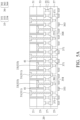
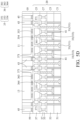
- the internal structure of the antenna-in-package construction 100 is shown in a partially transparent manner. In other words, when observing the side of the antenna-in-package construction 100 in reality, it may not be possible to see every component shown in FIG. 5A to FIG. 5D . Moreover, some components of the antenna-in-package construction 100 are omitted in FIG. 5A to FIG. 5D for the sake of brevity.
- the packaging stacked layer 20 sequentially includes a redistribution wiring layer 25, a grounding layer 27, a second dielectric layer 23, and a first dielectric layer 21.
- the transmitting array antenna 31 (that includes multiple first antennas 311) is disposed in the first dielectric layer 21 and extends from the first dielectric layer 21 to the redistribution wiring layer 25.
- the receiving array antenna 33 (that includes multiple second antennas 333) is disposed in the second dielectric layer 23 and extends from the second dielectric layer 23 to the redistribution wiring layer 25.
- Multiple metal isolation pillars 41 surround each first antenna 311 and each second antenna 333 to prevent the transmitting array antenna 31 and the receiving array antenna 33 from interfering with each other.
- the packaging stacked layer 20 is inverted, and multiple transmitting chips 11 and multiple receiving chips 13 are formed on the redistribution wiring layer 25 (only one transmitting chip 11 and one receiving chip 13 are illustrated in FIG. 5B ).
- the transmitting chips 11 are electrically connected to the transmitting array antenna 31, and the receiving chips 13 are electrically connected to the receiving array antenna 33.
- metal isolation pillars 43 are formed around the transmitting chips 11 and the receiving chips 12 to prevent the transmitting chips 11 and the receiving chips 12 from interfering with each other.
- conductive pillars 45 are also formed, but the present disclosure is not limited thereto.
- a protective material 59 is formed on the redistribution wiring layer 25.
- the protective material 59 is formed between the transmitting chips 11, the receiving chips 13, the metal isolation pillars 43, and the conductive pillars 45, exposing (at least part of) the surface of the transmitting chips 11, the receiving chips 13, the metal isolation pillars 43, and the conductive pillars 45.
- each metal isolation pillar 43 and each conductive pillar 45 are in direct contact with the corresponding solder ball 61.
- the antenna-in-package construction 100 may be electrically connected to another conductive substrate (not shown) through the solder balls 61, which is a type of flip-chip bonding, but the present disclosure is not limited thereto.
- the antenna-in-package construction 100 may also be electrically connected to another conductive substrate using wire bonding.
- the antenna-in-package construction may be arranged in an interleaved pattern between the transmitting array antenna and the receiving array antenna, approximating the aforementioned optimal space and optimal ratio to avoid interference between the uplink and downlink signals. Additionally, the antenna-in-package construction may also reduce issues such as the point errors of the antenna beam and grating lobes.
Landscapes
- Physics & Mathematics (AREA)
- Electromagnetism (AREA)
- Engineering & Computer Science (AREA)
- Microelectronics & Electronic Packaging (AREA)
- Variable-Direction Aerials And Aerial Arrays (AREA)
Abstract
Description
- This Application claims priority of
U.S. Application No. 18/468,779 , filed on September 18, andTaiwan Patent Application No. 112129752, filed on August 8, 2023 - The disclosure relates to an antenna-in-package construction, and in particular, relates to an antenna-in-package construction that includes a transmitting antenna array and a receiving antenna array arranged in an alternating interleaved sequence on the same plane, which can simultaneously transmit uplink signals and receive downlink signals in different frequency bands.
- With the development of 5G communication technology, it is anticipated that future trends will lead to a 6G communication technology. Recently, phased array antennas have been applied to satellite communications, particularly low-Earth orbit (LEO) satellite communications. Technically, LEO satellite communications can address the challenges faced in mobile communications, wherein radio frequency (RF) signals cannot cover rugged terrain. Moreover, from a business perspective, companies like Starlink and Amazon in the West have already launched satellites into low-Earth orbit, aiming to establish communications between ground-based transceivers and LEO satellites. This shows that the global market for ground communication equipment for LEO satellites is booming.
- A phased array antenna consists of multiple antennas combined with communication devices that control their phases. By adjusting the phase of each individual antenna, beams can be directed in specific orientations at different times and in different spatial regions. For example, a high-directivity array 32×32 antenna has a gain that is greater than 30 dBi and a beam width of less than 3.5°. The space between adjacent antennas can range from a half-wave length (λ/2) to a quarter-wave length (λ/4), with the preferred space being a half-wave length (λ/2). Additionally, these high-directivity array antennas also exhibit minimal point errors and reduced grating lobes.
- In reality, when a transceiver transmits RF signals (also referred to as uplink signals), it operates at frequencies from 27.5 GHz to 30 GHz. However, when the transceiver receives RF signals (also referred to as downlink signals), it operates from 17.7 GHz to 20.2 GHz. If a transceiver transmits and receives uplink and downlink signals in different frequency bands simultaneously, the uplink signal and the downlink signal may interfere with each other between the phase-array antenna at the transmitting end (also referred to as transmitting array antenna) and the phase-array antenna at the receiving end (also referred to as receiving array antenna). Moreover, with antenna-in-package construction, the space between transmitting array antennas is 5.36 mm, whereas the space between receiving array antennas is 8.33 mm. This results in the space between a transmitting antenna and the adjacent receiving antenna not adhering to the optimal ratio of

- To resolve the interference between uplink and downlink signals, a common solution is to arrange transmitting array antennas and receiving array antennas in a staggered arrangement. However, in this arrangement, because the area of the transmitting array antenna is smaller than the area of the receiving array antenna, the transmitting array antenna and the receiving array antenna partially overlap each other. Therefore, the uplink signal and downlink signal will still interfere with each other.
- Although the current transceiver is expected to encapsulate the above-mentioned antennas in a housing of the same size to effectively reduce the size of the transceiver, the aforementioned problems cannot be solved.
- The disclosure provides an antenna-in-package construction with frequency division duplex technology. The antenna-in-package construction includes a chip layer, a second dielectric layer, and a first dielectric layer having the same or a different dielectric constant than the second dielectric layer that are stacked in order, and further includes a transmitting array antenna, a receiving array antenna, and a plurality of metal isolation pillars. The first dielectric layer has a dielectric constant that is more than 3.5. The transmitting antenna array extends from the chip layer to the first dielectric layer through the second dielectric layer. The receiving antenna array extends from the chip layer to the second dielectric layer, wherein the transmitting antenna array and the receiving antenna array are arranged in an alternating interleaved sequence. The plurality of metal isolated pillars surround each transmitting antenna and each receiving antenna. Additionally, the chip layer includes at least one transmitting chip and at least one receiving chip. The transmitting chip is electrically connected to the transmitting antenna array, and the receiving chip is electrically connected to the receiving antenna array. The transmitting array antenna includes a plurality of first antennas, and each first antenna is spaced a first distance from the adjacent first antenna, wherein the first distance is close to a half-wave length. The receiving array antenna includes a plurality of second antennas, and each second antenna is spaced a second distance from the adjacent second antenna, wherein the second distance is close to the half-wave length and is different from the first distance.
- The present invention can be more fully understood by reading the subsequent detailed description and examples with references made to the accompanying drawings, wherein:
-
FIG. 1 is a partial side view illustrating an antenna-in-package construction according to an embodiment. -
FIG. 2 is a partial bottom view illustrating an antenna-in-package construction according to an embodiment. -
FIG. 3 is a schematic three-dimensional view illustrating an antenna-in-package construction according to an embodiment. -
FIG. 4 is a diagram illustrating a method for performing wireless communication according to an embodiment. -
FIG. 5A to FIG. 5D are partial side views of manufacturing the antenna-in-package construction at various stages according to an embodiment. - This embodiment discloses an antenna-in-
package construction 100, which measures 256x256 square millimeters (mm2) and is applied to frequency division duplex (FDD) technology in wireless communication systems. The antenna-in-package construction 100 may be composed of a Complementary Metal Oxide Semiconductor (CMOS) chip and a 1024 array antenna, wherein the CMOS chip is manufactured by advanced processes. The wireless communication system may be consist of low-Earth orbit satellites and ground-based transceivers and employ frequency division duplex technology. Frequency division duplex technology involves simultaneous transmitting uplink signals with a first frequency band and receiving downlink signals with a second frequency band. Here, the first frequency band is the Ka-band, while the second frequency band ranges from the Ku-band to the K-band. The first frequency band and the second frequency band are different. The Ka-band frequency ranges from about 27 GHz to 40 GHz, with a wavelength ranges from about 11.11 mm to 7.50 mm. The Ku-band frequency ranges from about 12 GHz to 18 GHz, with a wavelength ranges from about 25.00mm to 16.67 mm. The K-band frequency ranges from about 18 GHz to 27 GHz, with a wavelength ranges from about 16.67mm to 11.11 mm. - Referring to
Figure 1 , the antenna-in-package construction 100 includes achip layer 10 and a packaging stackedlayer 20. Thechip layer 10 includes one or more transmittingchips 11 andmultiple receiving chips 13. The transmitting chip (TX chip) includes a power amplifier (PA). The receiving chip (RX chip) includes a low noise amplifier (LNA). The packaging stackedlayer 20 includes a firstdielectric layer 21, a seconddielectric layer 23, aredistribution wiring layer 25, and agrounding layer 27. Moreover, as shown inFIG. 1 , in this embodiment, the packaging stackedlayer 20 further includes transmittingantenna arrays 31 and receivingantenna array 33 that are arranged in an alternating interleaved sequence, as well as multiplemetal isolation pillars - The
chip layer 10 may further include one or more radio frequency front-end modules (FEM), one or more analog beamforming circuits, and one or more digital beamforming (DBF) circuits. - In this embodiment, both the transmitting
chip 11 and receivingchip 13 may be made of silicon (Si), silicon germanium (SiGe), gallium nitride (GaN), gallium arsenide (GaAs), compound semiconductor, or any other suitable material. Optionally, thechip layer 10 may include an electromagnetic shielding layer. - The packaging stacked
layer 20 may be a multi-layer board that is consisted of two or more layers and include low-temperature co-fired ceramic (LTCC), FR-4 epoxy glass fabric, RO high-frequency circuit board, silicon, glass, gallium arsenide, silicon nitride, thermal interface materials (TIM), any other suitable material, or a combination thereof. The thermal interface materials may include thermal grease, thermal gel, phase-change materials, phase-change metal alloys, thermally conductive adhesives, any other suitable material, or a combination thereof. - The
first dielectric layer 21 is composed of a firstdielectric material 51 and is disposed above thechip layer 10, wherein the firstdielectric material 51 fills the spaces excluding the transmittingarray antenna 31 and themetal isolation pillars 41. In this embodiment, the dielectric constant of the firstdielectric material 51 is higher than the dielectric constant of air. For instance, the dielectric constant of the firstdielectric material 51 may range from about 3 to 13, such as from about 3 to 4 (e.g., polyimide with a dielectric constant of about 3.5) or from about 10 to 13 (e.g., silicon with a dielectric constant of about 11.9 or gallium arsenide with a dielectric constant of about 12.9). The firstdielectric material 51 may include any suitable dielectric material, such as low-temperature co-fired ceramic (LTCC), FR-4 epoxy glass fabric, RO high-frequency circuit board, silicon, glass, gallium arsenide, thermal interface materials (TIM), photosensitive materials (e.g., polyimide), any other suitable high dielectric constant material, or a combination thereof, but is not limited thereto. - The
second dielectric layer 23 is composed of a seconddielectric material 53 and is disposed between thechip layer 10 and thefirst dielectric layer 21. The seconddielectric material 53 fills the spaces excluding the transmittingarray antenna 31, receivingarray antenna 33, andmetal isolation pillars 41. In this embodiment, the seconddielectric material 53 may be the same or similar to the firstdielectric material 51, but the present disclosure is not limited thereto. In this embodiment, the dielectric constant of the seconddielectric material 53 is less than that of the firstdielectric material 51. - The
redistribution wiring layer 25 is disposed between thechip layer 10 and thesecond dielectric layer 23 and includes a first antenna chipconductive wire 35 and a second antenna chipconductive wire 36. The first antenna chipconductive wire 35 includes (or is divided into) multipleconductive wires conductive wires array antenna 31 with the transmittingchip 11. The second antenna chipconductive wire 36 includes (or is divided into) multipleconductive wires conductive wires array antenna 33 with the receivingchip 13. Theconductive wires - The
grounding layer 27 is disposed between theredistribution wiring layer 25 and thesecond dielectric layer 23. Thegrounding layer 27 includesmultiple grounding pillars 37 that ground themetal isolation pillars 41. In addition, theredistribution wiring layer 25 also includes multiple groundingconductive wires 371. The groundingpillars 37 ground themetal isolation pillars 41 through the groundingconductive wires 371. The groundingpillars 37 and the groundingconductive wires 371 may include materials that are the same or similar to theconductive wires - The transmitting
array antenna 31 includes multiple first antennas 311 (also referred to as transmitting antennas) and extends from thefirst dielectric layer 21 to thechip layer 10 to be electrically connected to thetransmitting chip 11. Furthermore, the distance between eachfirst antenna 311 and the adjacentfirst antenna 311 is the first distance (λU), which is close to a half-wave length. - The receiving
array antenna 33 includes multiple second antennas 333 (also referred to as receiving antennas) and extends from thesecond dielectric layer 23 to thechip layer 10 to be electrically connected to the receivingchip 13. Furthermore, the distance between eachsecond antenna 333 and the adjacentsecond antenna 333 is the second distance (λD), which is close to the half-wave length, wherein the second distance and the first distance may be the same or different. For example, the first distance is 0.528λU = 0.528×5.36 = 2.83008 millimeters (mm), the second distance is 0.48λD = 0.48×8.33 = 3.9984 millimeters (mm), and the ratio of the first distance to the second distance is 0.707. - In this embodiment, the transmitting
array antenna 31 and the receivingarray antenna 33 may include gold, tin, silver, copper, nickel, any other suitable metal or alloy. Moreover, the transmittingarray antenna 31 and the receivingarray antenna 33 may be formed by processes like electroplating, chemical plating, printing processes, other suitable processes or combinations thereof, but the present disclosure is not limited thereto. - In this embodiment, the number of transmitting
array antennas 31 may be an integer multiple of the number of receivingarray antennas 33, preferably twice as many. For example, there are 128first antennas 311 in the transmittingarray antenna 31, while there are 64second antennas 333 in the receivingarray antenna 33. - The
metal isolation pillars 41 surround eachfirst antenna 311 and eachsecond antenna 333 to prevent thefirst antenna 311 and thesecond antenna 333 from interfering with each other. Themetal isolation pillar 41 may include metals, such as gold (Au), nickel (Ni), platinum (Pt), palladium (Pd), iridium (Ir), titanium (Ti), chromium (Cr), tungsten (W), aluminum (Al), copper (Cu), tin (Sn), silver (Ag), a similar material, an alloy thereof, or a combination thereof. In this embodiment, themetal isolation pillars 41 are made of copper, but the present disclosure is not limited thereto. - The
metal isolation pillars 43 surround thetransmitting chip 11 and the receiving chip 12 to prevent thetransmitting chip 11 and receiving chip 12 from interfering with each other. For example, themetal isolation pillar 43 may include materials that are the same as or similar or themetal isolation pillar 41, which will not be repeated here, but the present disclosure is not limited thereto. - Referring to
FIG. 1 andFIG. 2 , in this embodiment, multiplefirst antennas 311 are arranged in one (or more) array(s), multiplesecond antennas 333 are arranged in one (or more) array(s), and thefirst antennas 311 and thesecond antennas 333 are arranged in an interleaved sequence. As shown inFIG. 1 andFIG. 2 , in this embodiment, each transmittingchip 11 is electrically connected to four first antennas 311 (as shown in region E1 inFIG. 2 ), and each receivingchip 13 is electrically connected to four second antennas 333 (as shown in region E2 inFIG. 2 ), but the present disclosure is not limited thereto. In this embodiment, each transmittingchip 11 is electrically connected with two or more than fourfirst antennas 311, and each receivingchip 13 is electrically connected with two or more than foursecond antennas 333. The arrangement and (electrical) connection of the transmittingarray antenna 31 and receivingarray antenna 33 may be designed or adjusted according to actual needs. - In the bottom view, after rotating each
first antenna 311 by 45 degrees, eachsecond antenna 333 has the same shape as eachfirst antenna 311 but with different sizes. For instance, the top surfaces of both thefirst antenna 311 and thesecond antenna 333 are shaped like a clover. Furthermore, the top area of thefirst antenna 311 is smaller than the top area of thesecond antenna 333, but the present disclosure is not limited thereto. - Similarly, in the bottom view, the top surfaces of the
first antenna 311 and thesecond antenna 333 may be rectangles, circles, ellipses, or other shapes, or the top area of thefirst antenna 311 may be equal to the top area of thesecond antenna 333. For example, eachfirst antenna 311 is a rectangle, and eachsecond antenna 333 is a diamond formed by rotating a rectangle, with the edge corner of the diamond that faces one side edge of the adjacent rectangle. - Similarly, in the bottom view, after rotating each receiving
chip 13 by 45 degrees, each receivingchip 13 has the same shape as each transmittingchip 11 but with different sizes. For instance, the top surfaces of both thetransmitting chip 11 and the receivingchip 13 are rectangular, and the top area of the transmittingchip 11 is smaller than the top area of the receivingchip 13, but the present disclosure is not limited thereto. In this embodiment, the top surfaces of the transmittingchip 11 and the receivingchip 13 may be other shapes, or the top area of the transmittingchip 11 may be equal to the top area of the receivingchip 13. - Similarly, the antenna-in-
package construction 100 further includesdielectric layers dielectric layer 55 is disposed within thegrounding layer 27 and fills the spaces excluding the transmittingarray antenna 31, the receivingarray antenna 33, and thegrounding pillars 37. Thedielectric layer 57 is disposed within theredistribution wiring layer 25 and fills the spaces excluding the conductingwires conductive wire 371, but the present disclosure is not limited thereto. - In this embodiment, the transmitting
array antenna 31 operates in the first frequency band, while the receivingarray antenna 33 operates in the second frequency band. The first frequency band is determined by the top area of thefirst antenna 311 and the dielectric constant of thedielectric layer 51, whereas the second frequency band is determined by the top area of thesecond antenna 333 and the dielectric constant of thedielectric layer 53. - In this embodiment, the antenna-in-
package construction 100 further includesconductive pillars 45 disposed within thechip layer 10 for electrically connecting other conductive components in the chip layer 10 (e.g., other chips, conductive pads, etc.) to external or internal components of the antenna-in-package construction 100. - In this embodiment, the antenna-in-
package construction 100 includes aprotective material 59 disposed within thechip layer 10 and fills the space excluding the transmittingchip 11, the receivingchip 13, themetal isolation pillars 43, and theconductive pillars 45, but the present disclosure is not limited thereto. Theprotective material 59 may include molding compounds, mold underfill (MUF), other suitable materials, or a combination thereof, but the present disclosure is not limited thereto. - Referring to
FIG. 3 , multiple packaging stackedlayers 20 are respectively disposed above thecorresponding chip layer 10. Here, each packaging stackedlayer 20 may include at least one region E1 (i.e., a transmittingchip 11 is electrically connected to four first antennas 311) and region E2 (i.e., a receivingchip 13 is electrically connected to four second antennas 333). In other words, inFIG. 3 , the antenna-in-package construction 100 may include sixteen transmittingchips 11 with their corresponding sixty-fourfirst antennas 311, and sixteen receivingchips 13 with their corresponding sixty-foursecond antennas 333, but the present disclosure is not limited thereto. - Referring again to
FIG. 3 , regarding the manufacturing method of the antenna-in-package construction 100, the panel-level package (PLP) process may be adopted, which uses large-area substrates to enhance the production of massive planar antenna arrays. - In this embodiment, the interleaved array of the antenna-in-
package construction 100 may support multi-band receiving/transmitting antenna arrays. It may perform frequency division duplexing (FDD) communication processing in the mobile devices of wireless communication systems, integrating both the transmitting antenna (TX) and the receiving antenna (RX) into a single module for miniaturization, thereby replacing the traditional two sets of non-shared antenna structures. Furthermore, according to the embodiment, the antenna-in-package construction 100 may overcome issues such as mutual interference between the transmitting antenna (TX) and the receiving antenna (RX), point error of the antenna beam, and grating lobes caused by the gap between the uplink and downlink carrier frequencies in the Ka-band. - Referring to
FIG. 4 , through the antenna-in-package construction 100, frequency division duplexing is implemented. The transmission signal TX emitted by the transmittingchip 11 is transmitted to the transmittingarray antenna 31 through the first antenna chipconductive wire 35 and emitted outside the antenna-in-package construction 100. At the same time, the reception signal RX received by the receivingarray antenna 33 is transmitted to the receivingchip 33 for signal processing through the second antenna chipconductive wire 36. In this embodiment, the transmittingarray antenna 31 operates at the first frequency band, the receivingarray antenna 33 operates at the second frequency band, and the first frequency band and the second frequency band are different. - Unlike time division duplexing (TDD), frequency division duplexing uses two frequency channels to transmit and receive signals. Because the operation time is continuous, during high-speed movement (e.g., on a high-speed train or receiving signals from low-Earth orbit satellites), the resource allocation of frequency division duplexing is large. Electronic devices (e.g., mobile phones) that include the antenna-in-
package construction 100 transmit (uplink) and receive (downlink) simultaneously. If the electronic device detects a deterioration in the quality of the receiving channel (downlink), it can quickly inform the base station (e.g., a cellular base station or low-Earth orbit satellite) for adjustments through the transmitting channel (uplink). - Referring to
FIG. 5A to FIG. 5D , the internal structure of the antenna-in-package construction 100 is shown in a partially transparent manner. In other words, when observing the side of the antenna-in-package construction 100 in reality, it may not be possible to see every component shown inFIG. 5A to FIG. 5D . Moreover, some components of the antenna-in-package construction 100 are omitted inFIG. 5A to FIG. 5D for the sake of brevity. - Referring to
FIG. 5A , a method for manufacturing the packaging stackedlayer 20 is provided. The packaging stackedlayer 20 sequentially includes aredistribution wiring layer 25, agrounding layer 27, asecond dielectric layer 23, and afirst dielectric layer 21. The transmitting array antenna 31 (that includes multiple first antennas 311) is disposed in thefirst dielectric layer 21 and extends from thefirst dielectric layer 21 to theredistribution wiring layer 25. The receiving array antenna 33 (that includes multiple second antennas 333) is disposed in thesecond dielectric layer 23 and extends from thesecond dielectric layer 23 to theredistribution wiring layer 25. Multiplemetal isolation pillars 41 surround eachfirst antenna 311 and eachsecond antenna 333 to prevent the transmittingarray antenna 31 and the receivingarray antenna 33 from interfering with each other. - Referring to
FIG. 5B , the packaging stackedlayer 20 is inverted, and multiple transmittingchips 11 and multiple receivingchips 13 are formed on the redistribution wiring layer 25 (only onetransmitting chip 11 and onereceiving chip 13 are illustrated inFIG. 5B ). The transmitting chips 11 are electrically connected to the transmittingarray antenna 31, and the receivingchips 13 are electrically connected to the receivingarray antenna 33. - Referring to
FIG. 5C ,metal isolation pillars 43 are formed around the transmittingchips 11 and the receiving chips 12 to prevent the transmittingchips 11 and the receiving chips 12 from interfering with each other. In this embodiment, when forming themetal isolation pillars 43,conductive pillars 45 are also formed, but the present disclosure is not limited thereto. - Referring to
FIG. 5D , aprotective material 59 is formed on theredistribution wiring layer 25. In more detail, theprotective material 59 is formed between the transmittingchips 11, the receivingchips 13, themetal isolation pillars 43, and theconductive pillars 45, exposing (at least part of) the surface of the transmittingchips 11, the receivingchips 13, themetal isolation pillars 43, and theconductive pillars 45. - Then, referring back to
FIG. 1 ,multiple solder balls 61 are formed and connected to themetal isolation pillars 43 and theconductive pillars 45 to form the antenna-in-package construction 100. More specifically, eachmetal isolation pillar 43 and eachconductive pillar 45 are in direct contact with thecorresponding solder ball 61. Finally, the antenna-in-package construction 100 may be electrically connected to another conductive substrate (not shown) through thesolder balls 61, which is a type of flip-chip bonding, but the present disclosure is not limited thereto. In this embodiment, the antenna-in-package construction 100 may also be electrically connected to another conductive substrate using wire bonding. - In summary, according to the embodiment, the antenna-in-package construction may be arranged in an interleaved pattern between the transmitting array antenna and the receiving array antenna, approximating the aforementioned optimal space and optimal ratio to avoid interference between the uplink and downlink signals. Additionally, the antenna-in-package construction may also reduce issues such as the point errors of the antenna beam and grating lobes.
Claims (15)
- An antenna-in-package construction with transmit an uplink signal and receive a downlink signal that have different frequency bands, comprising:a chip layer (10) comprising at least one transmitting chip (11) and at least one receiving chip (13);a first dielectric layer (21) on the chip layer, wherein the first dielectric has a dielectric constant that is higher than 3.5;a second dielectric layer (23) between the chip layer and the first dielectric layer;a transmitting array antenna (31) comprising a plurality of first antennas (311), electrically connected to the transmitting chip and extending from the transmitting chip to the first dielectric layer, wherein each of the first antennas is spaced a first distance from an adjacent one of the first antennas, and the first distance is close to a half-wave length;a receiving array antenna (33) comprising a plurality of second antennas (333), electrically connected to the receiving chip and extending from the receiving chip to the second dielectric layer, wherein each of the second antennas and each of the first antennas are arranged in a staggered manner on a same plane, and each of the second antennas is spaced a second distance from an adjacent one of the second antennas, and the second distance is close to the half-wave length and is different from the first distance; anda plurality of metal isolation pillars (41) surrounding each of the first antennas and each of the second antennas.
- The antenna-in-package construction as claimed in claim 1, wherein the first distance is less than the second distance.
- The antenna-in-package construction as claimed in claims 1 or 2, wherein on the same plane, an area of each of the first antennas is different from an area of each of the second antennas.
- The antenna-in-package construction as claimed in any of claims 1 to 3, wherein on the same plane, an area of each of the first antennas is smaller than an area of each of the second antennas.
- The antenna-in-package construction as claimed in any of claims 1 to 4, wherein on the same plane, a length of each of the first antennas is longer than a length of each of the second antennas.
- The antenna-in-package construction as claimed in any of claims 1 to 5, wherein each of the first antennas comprises at least one side edge, and each of the second antennas includes at least one edge corner, wherein the edge corner of the second antenna faces the side edge of an adjacent one of the first antennas.
- The antenna-in-package construction as claimed in any of claims 1 to 6, wherein on the same plane, each of the first antennas and each of the second antennas have the same shape.
- The antenna-in-package construction as claimed in any of claims 1 to 7, wherein the number of transmitting array antennas is an integer multiple of the number of receiving array antennas.
- The antenna-in-package construction as claimed in any of claims 1 to 8, wherein the uplink signal has a first frequency band ranging from 27 GHz to 40 GHz, and the downlink signal has a second frequency band ranging from 17 GHz to 27 GHz.
- The antenna-in-package construction as claimed in any of claims 1 to 9, wherein a dielectric constant of the second dielectric layer is different from a dielectric constant of the first dielectric layer.
- The antenna-in-package construction as claimed in any of claims 1 to 9, wherein the dielectric constant of the second dielectric layer is the same as the dielectric constant of the first dielectric layer.
- The antenna-in-package construction as claimed in any of claims 1 to 11, further comprising:
a redistribution wiring layer (25) comprising a plurality of conductive lines (35, 36) and disposed between the chip layer and the second dielectric layer, wherein the redistribution wiring layer is used for electrically connecting each of the first antennas to the transmitting chip and electrically connecting each of the second antennas to the receiving chip. - The antenna-in-package construction as claimed in any of claims 1 to 12, wherein the metal isolation pillars are also around the transmitting chip and the receiving chip.
- The antenna-in-package construction as claimed in any of claims 1 to 13, further comprising:
a grounding layer (27) comprising a plurality of grounding pillars (37), wherein the grounding layer is used for grounding the metal isolation pillars. - The antenna-in-package construction as claimed in any of claims 1 to 14, wherein each of the first antennas extends from the transmitting chip to the second dielectric layer instead of the first dielectric layer; and each of the second antennas extends from the receiving chip to the first dielectric layer instead of the second dielectric layer.
Applications Claiming Priority (2)
| Application Number | Priority Date | Filing Date | Title |
|---|---|---|---|
| TW112129752A TWI867674B (en) | 2023-08-08 | 2023-08-08 | Antenna-in-package construction with frequency division duplex technology |
| US18/468,779 US12374794B2 (en) | 2023-08-08 | 2023-09-18 | Antenna-in-package construction with frequency division duplex technology |
Publications (2)
| Publication Number | Publication Date |
|---|---|
| EP4507120A1 true EP4507120A1 (en) | 2025-02-12 |
| EP4507120B1 EP4507120B1 (en) | 2026-05-06 |
Family
ID=88412137
Family Applications (1)
| Application Number | Title | Priority Date | Filing Date |
|---|---|---|---|
| EP23203470.2A Active EP4507120B1 (en) | 2023-08-08 | 2023-10-13 | Antenna-in-package construction with frequency division duplex technology |
Country Status (1)
| Country | Link |
|---|---|
| EP (1) | EP4507120B1 (en) |
Citations (4)
| Publication number | Priority date | Publication date | Assignee | Title |
|---|---|---|---|---|
| US10505255B2 (en) * | 2017-01-30 | 2019-12-10 | Infineon Technologies Ag | Radio frequency device packages and methods of formation thereof |
| US20200035625A1 (en) * | 2018-07-27 | 2020-01-30 | Taiwan Semiconductor Manufacturing Co., Ltd. | Package, package structure and method of manufacturing the same |
| US20200185299A1 (en) * | 2016-06-24 | 2020-06-11 | Agency For Science, Technology And Research | Semiconductor package and method of forming the same |
| US11217543B2 (en) * | 2017-11-03 | 2022-01-04 | Samsung Electronics Co., Ltd. | Antenna module |
Family Cites Families (1)
| Publication number | Priority date | Publication date | Assignee | Title |
|---|---|---|---|---|
| TWM637071U (en) * | 2022-07-14 | 2023-02-01 | 周錫增 | Array type radio frequency device |
-
2023
- 2023-10-13 EP EP23203470.2A patent/EP4507120B1/en active Active
Patent Citations (4)
| Publication number | Priority date | Publication date | Assignee | Title |
|---|---|---|---|---|
| US20200185299A1 (en) * | 2016-06-24 | 2020-06-11 | Agency For Science, Technology And Research | Semiconductor package and method of forming the same |
| US10505255B2 (en) * | 2017-01-30 | 2019-12-10 | Infineon Technologies Ag | Radio frequency device packages and methods of formation thereof |
| US11217543B2 (en) * | 2017-11-03 | 2022-01-04 | Samsung Electronics Co., Ltd. | Antenna module |
| US20200035625A1 (en) * | 2018-07-27 | 2020-01-30 | Taiwan Semiconductor Manufacturing Co., Ltd. | Package, package structure and method of manufacturing the same |
Also Published As
| Publication number | Publication date |
|---|---|
| EP4507120B1 (en) | 2026-05-06 |
Similar Documents
| Publication | Publication Date | Title |
|---|---|---|
| Gu et al. | Development, implementation, and characterization of a 64-element dual-polarized phased-array antenna module for 28-GHz high-speed data communications | |
| CN111247695B (en) | Wideband stacked patch radiating element and associated phased array antenna | |
| US10714829B2 (en) | Planar phased array antenna | |
| US8018384B2 (en) | Method and apparatus for packaging an integrated chip and antenna | |
| US10587044B2 (en) | Flip-chip beamforming integrated circuit with integral thermal mass | |
| US11936125B2 (en) | Antenna module and communication device equipped with the same | |
| WO2020241271A1 (en) | Sub-array antenna, array antenna, antenna module, and communication device | |
| Rebeiz et al. | Advances in SATCOM phased arrays using silicon technologies | |
| US20210083380A1 (en) | Antenna module and communication device equipped with the same | |
| US12206179B2 (en) | Antenna module and communication device equipped with the same | |
| Jin et al. | Antenna-in-package design based on wafer-level packaging with through silicon via technology | |
| US11177227B2 (en) | Method and apparatus for heat sinking high frequency IC with absorbing material | |
| CN110890331A (en) | Semiconductor device package and method of manufacturing the same | |
| US11916312B2 (en) | Antenna module, communication device mounting the same, and circuit board | |
| US20210043996A1 (en) | Thermal management method and apparatus for high frequency ic with apertured heat sink | |
| US20180054005A1 (en) | Hybrid Laminated Phased Array | |
| US12374794B2 (en) | Antenna-in-package construction with frequency division duplex technology | |
| CN118919495A (en) | AIP airtight packaging structure based on LTCC packaging substrate and antenna wiring cover plate | |
| US20240145941A1 (en) | Electronic device | |
| EP4507120B1 (en) | Antenna-in-package construction with frequency division duplex technology | |
| Rebeiz et al. | Advances in low-cost phased arrays using silicon technologies | |
| US7163155B2 (en) | ASIC-embedded switchable antenna arrays | |
| Sadhu et al. | A Heterogeneously Integrated 256-Element 5G Phased Array: Design, Assembly, Test | |
| US20260066523A1 (en) | Packaging structure and manufacturing method thereof | |
| US10505276B2 (en) | Wireless communications assembly with integrated active phased-array antenna |
Legal Events
| Date | Code | Title | Description |
|---|---|---|---|
| PUAI | Public reference made under article 153(3) epc to a published international application that has entered the european phase |
Free format text: ORIGINAL CODE: 0009012 |
|
| STAA | Information on the status of an ep patent application or granted ep patent |
Free format text: STATUS: REQUEST FOR EXAMINATION WAS MADE |
|
| 17P | Request for examination filed |
Effective date: 20240816 |
|
| AK | Designated contracting states |
Kind code of ref document: A1 Designated state(s): AL AT BE BG CH CY CZ DE DK EE ES FI FR GB GR HR HU IE IS IT LI LT LU LV MC ME MK MT NL NO PL PT RO RS SE SI SK SM TR |
|
| GRAP | Despatch of communication of intention to grant a patent |
Free format text: ORIGINAL CODE: EPIDOSNIGR1 |
|
| STAA | Information on the status of an ep patent application or granted ep patent |
Free format text: STATUS: GRANT OF PATENT IS INTENDED |
|
| RIC1 | Information provided on ipc code assigned before grant |
Ipc: H01Q 1/22 20060101AFI20260125BHEP Ipc: H10W 42/20 20260101ALI20260125BHEP Ipc: H10W 44/20 20260101ALI20260125BHEP Ipc: H01Q 1/52 20060101ALI20260125BHEP Ipc: H01Q 5/42 20150101ALI20260125BHEP Ipc: H01Q 21/06 20060101ALI20260125BHEP |
|
| INTG | Intention to grant announced |
Effective date: 20260205 |
|
| GRAS | Grant fee paid |
Free format text: ORIGINAL CODE: EPIDOSNIGR3 |
|
| GRAA | (expected) grant |
Free format text: ORIGINAL CODE: 0009210 |
|
| STAA | Information on the status of an ep patent application or granted ep patent |
Free format text: STATUS: THE PATENT HAS BEEN GRANTED |
|
| AK | Designated contracting states |
Kind code of ref document: B1 Designated state(s): AL AT BE BG CH CY CZ DE DK EE ES FI FR GB GR HR HU IE IS IT LI LT LU LV MC ME MK MT NL NO PL PT RO RS SE SI SK SM TR |
|
| REG | Reference to a national code |
Ref country code: CH Ref legal event code: F10 Free format text: ST27 STATUS EVENT CODE: U-0-0-F10-F00 (AS PROVIDED BY THE NATIONAL OFFICE) Effective date: 20260506 Ref country code: GB Ref legal event code: FG4D |