EP4503904A1 - Quantum device and method for manufacturing quantum device - Google Patents
Quantum device and method for manufacturing quantum device Download PDFInfo
- Publication number
- EP4503904A1 EP4503904A1 EP22935529.2A EP22935529A EP4503904A1 EP 4503904 A1 EP4503904 A1 EP 4503904A1 EP 22935529 A EP22935529 A EP 22935529A EP 4503904 A1 EP4503904 A1 EP 4503904A1
- Authority
- EP
- European Patent Office
- Prior art keywords
- substrate
- quantum
- pads
- substrates
- base member
- Prior art date
- Legal status (The legal status is an assumption and is not a legal conclusion. Google has not performed a legal analysis and makes no representation as to the accuracy of the status listed.)
- Pending
Links
Images













Classifications
-
- H—ELECTRICITY
- H10—SEMICONDUCTOR DEVICES; ELECTRIC SOLID-STATE DEVICES NOT OTHERWISE PROVIDED FOR
- H10N—ELECTRIC SOLID-STATE DEVICES NOT OTHERWISE PROVIDED FOR
- H10N69/00—Integrated devices, or assemblies of multiple devices, comprising at least one superconducting element covered by group H10N60/00
-
- G—PHYSICS
- G06—COMPUTING OR CALCULATING; COUNTING
- G06N—COMPUTING ARRANGEMENTS BASED ON SPECIFIC COMPUTATIONAL MODELS
- G06N10/00—Quantum computing, i.e. information processing based on quantum-mechanical phenomena
- G06N10/40—Physical realisations or architectures of quantum processors or components for manipulating qubits, e.g. qubit coupling or qubit control
-
- H—ELECTRICITY
- H10—SEMICONDUCTOR DEVICES; ELECTRIC SOLID-STATE DEVICES NOT OTHERWISE PROVIDED FOR
- H10W—GENERIC PACKAGES, INTERCONNECTIONS, CONNECTORS OR OTHER CONSTRUCTIONAL DETAILS OF DEVICES COVERED BY CLASS H10
- H10W20/00—Interconnections in chips, wafers or substrates
- H10W20/20—Interconnections within wafers or substrates, e.g. through-silicon vias [TSV]
-
- H—ELECTRICITY
- H10—SEMICONDUCTOR DEVICES; ELECTRIC SOLID-STATE DEVICES NOT OTHERWISE PROVIDED FOR
- H10W—GENERIC PACKAGES, INTERCONNECTIONS, CONNECTORS OR OTHER CONSTRUCTIONAL DETAILS OF DEVICES COVERED BY CLASS H10
- H10W72/00—Interconnections or connectors in packages
- H10W72/20—Bump connectors, e.g. solder bumps or copper pillars; Dummy bumps; Thermal bumps
- H10W72/251—Materials
- H10W72/252—Materials comprising solid metals or solid metalloids, e.g. PbSn, Ag or Cu
-
- H—ELECTRICITY
- H10—SEMICONDUCTOR DEVICES; ELECTRIC SOLID-STATE DEVICES NOT OTHERWISE PROVIDED FOR
- H10W—GENERIC PACKAGES, INTERCONNECTIONS, CONNECTORS OR OTHER CONSTRUCTIONAL DETAILS OF DEVICES COVERED BY CLASS H10
- H10W90/00—Package configurations
Definitions
- the present disclosure relates to a quantum device and a method for manufacturing the quantum device.
- An object of the present disclosure is to provide a quantum device capable of stabilizing the capacitance between quantum bits, and a method for manufacturing the quantum device.
- a quantum device includes: a first substrate; and a plurality of second substrates placed on the first substrate.
- the first substrate includes: a first base member that has a first surface; a plurality of first pads provided on the first surface; and a wiring line that couples two first pads of the plurality of first pads, each of the plurality of second substrates includes: a second base member that has a second surface that faces the first surface; a second pad that is provided on the second surface and faces the first pad; and a quantum bit coupled to the second pad, a quantum bit included in one second substrate of the plurality of second substrates and a quantum bit included in another one second substrate of the plurality of second substrates are capacitively coupled to each other via the wiring line.
- the quantum device includes an alignment mechanism that restrains each of the plurality of second substrates within a predetermined region in a plane parallel to the first surface of the first substrate.
- capacitance between quantum bits can be stabilized.
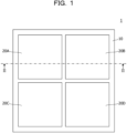
- FIG. 1 is a top view illustrating the quantum device according to the first embodiment.
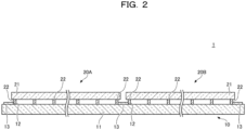
- FIG. 2 is a cross-sectional view illustrating the quantum device according to the first embodiment.
- FIG. 3 is a bottom view illustrating a quantum bit substrate included in the quantum device according to the first embodiment.
- FIG. 4 is a schematic diagram illustrating a positional relationship between four quantum bit substrates in the quantum device according to the first embodiment.
- FIG. 5 is a cross-sectional view illustrating a coupling relationship between two quantum bit substrates in the quantum device according to the first embodiment.
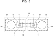
- FIG. 6 is a schematic diagram illustrating a coupling relationship between two quantum bit substrates in the quantum device according to the first embodiment.
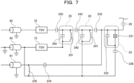
- FIG. 7 is a partial equivalent circuit diagram of the quantum device according to the first embodiment.
- FIG. 2 corresponds to a cross-sectional view taken along the line II-II in FIG. 1 .
- FIG. 5 corresponds to a cross-sectional view taken along the line V-V in FIG. 4 .
- a quantum device 1 includes a carrier substrate 10, a quantum bit substrate 20A, a quantum bit substrate 20B, a quantum bit substrate 20C, and a quantum bit substrate 20D.
- the carrier substrate 10 is an example of the first substrate
- the quantum bit substrates 20A to 20D are an example of the second substrates.
- the number of quantum bit substrates is not limited as long as it is two or larger.
- the carrier substrate 10 includes a base member 11, and protruding portions 13 formed on the upper surface of the base member 11.
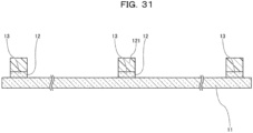
- the base member 11 and the protruding portions 13 are formed with silicon, for example. Although the details will be described later, four cavities 12 are formed in a silicon substrate, so that the base member 11 and the protruding portions 13 are formed.
- the protruding portions 13 are provided at a plurality of locations on the upper surface of the base member 11, and the protruding portions 13 provided at the plurality of locations integrally constitute a frame.
- the height of the protruding portions 13 is about 2 ⁇ m to 4 ⁇ m, for example.
- the upper surface of the base member 11 is an example of the first surface.
- the protruding portions 13 are part of the alignment mechanism.
- the quantum bit substrates 20A to 20D have the same configurations as one another. In the following description of the quantum bit substrates 20A to 20D, only the quantum bit substrate 20A will be explained as a typical example.
- the quantum bit substrate 20A includes a base member 21, and a plurality of first spacers 22 provided on the lower surface of the base member 21.
- part of the plurality of first spacers 22 is formed in the shape of a rectangular frame, and part of the outer surface of each first spacer 22 is in contact with part of the inner surface of a protruding portion 13 (see FIG. 5 ).
- part of the plurality of first spacers 22 is provided to have a cross shape, for example, inside a first spacer 22 formed in the shape of a rectangular frame.
- the lower surface of each first spacer 22 is in contact with the upper surface of the base member 11 of the carrier substrate 10.
- Each first spacer 22 is an Al layer, for example.
- the height of the first spacers 22 is 4 ⁇ m to 6 ⁇ m, for example, and is greater than the height of the protruding portions 13.
- the lower surface of the base member 21 is an example of the second surface.
- the first spacers 22 are part of the alignment mechanism.
- the quantum bit substrate 20A includes quantum bits (qubits) 23, resonators 24, filters 25, pads 33, a control port 61, a read port 62, and a ground port 63.
- Each quantum bit 23 is an element that forms a coherent two-level system using superconduction, and has a configuration that includes a transmon quantum bit circuit in which a superconducting Josephson element 231 and a capacitor 232 are coupled in parallel.
- the superconducting Josephson element 231 includes a pair of superconductors that exhibit superconductivity at a temperature equal to or lower than a predetermined critical temperature, and an ultrathin insulator that has a thickness of about several nanometers and is sandwiched between the pair of superconductors.
- the superconductor may be aluminum, for example, and the insulator may be aluminum oxide, for example.
- a plurality of quantum bits 23 is coupled to adjacent other quantum bits 23 via inter-bit wiring lines 27.
- Capacitors 28 are provided in the paths of the inter-bit wiring lines 27.
- each of the quantum bits 23 creates a quantum entangled state with the adjacent other quantum bits 23, and performs quantum computing.
- the intervals between the quantum bits 23 are about 2 mm, for example.
- a superconducting inductor 236 is coupled between each quantum bit 23 and the ground.
- FIG. 7 illustrates only the components in the vicinity of one quantum bit 23.
- the resonators 24 interact with the quantum bits 23, to read bit signals indicating the states of the quantum bits 23.
- the resonators 24 are coupled to the quantum bits 23 via capacitors 233.
- Each resonator 24 includes a resonance circuit in which a superconducting inductor 241 and a capacitor 242 are coupled in parallel.
- the filters 25 are coupled to the resonators 24 via capacitors 243.
- Each filter 25 includes a circuit in which a superconducting inductor 251 and a capacitor 252 are coupled in parallel.
- the pads 33 are coupled to some of the quantum bits 23, and are used for coupling to quantum bits 23 provided on the quantum bit substrate 20B or 20C.
- the pads 33 have a square planar shape, with a side length of about 200 ⁇ m, for example.
- the pads 33 are an example of the second pads.
- the distance between the pads 33 and the first spacer 22 is about 100 ⁇ m to 200 ⁇ m, for example. This is to avoid coupling between the pads 33 and the first spacer 22.
- each filter 25 For example, four sets of resonators 24 and quantum bits 23 are coupled to each filter 25.
- the quantum bits 23, the resonators 24, the filters 25, and the pads 33 are provided on the lower surface of the base member 21.
- the control port 61, the read port 62, and the ground port 63 are access ports for accessing a quantum computing circuit including the quantum bits 23, the resonators 24, and the filters 25, from the outside.
- the control port 61, the read port 62, and the ground port 63 are provided on the upper surface of the base member 21.
- the control port 61 is coupled to each quantum bit 23 via a capacitor 234.
- the control port 61 is used to control the quantum bits 23 from the outside.
- a superconducting inductor 235 is coupled between the ground and the wiring line between the control port 61 and the capacitor 234.
- the read port 62 is coupled to each filter 25 via a through silicon via (TSV) 72 provided on the base member 21 and a capacitor 253.
- TSV through silicon via
- the read port 62 is used to extract bit signals read by the resonators 24 to the outside.
- the ground port 63 is coupled to the quantum bits 23, the resonators 24, and the filters 25 via the TSV 73.
- the ground port 63 is used to apply a ground potential to the quantum bits 23, the resonator 24, and the filters 25, from the outside.
- through holes 21A and 21B are formed in the base member 21.
- the pads 33, the quantum bits 23, a superconductor layer 32, and a superconductor layer 38 are provided on the lower surface of the base member 21.
- the pads 33 and the quantum bits 23 are coupled to each other.
- the superconductor layer 32 forms the resonators 24 and the filters 25, and is coupled to the quantum bits 23.
- the superconductor layer 32 is adjacent to the through hole 21A.
- the superconductor layer 38 is adjacent to the through hole 21B.
- the pads 33, the superconductor layer 32, and the superconductor layer 38 are TiN layers, for example.
- the thicknesses of the pads 33, the superconductor layer 32, and the superconductor layer 38 are about 100 nm, for example.
- a superconductor layer 34, a superconductor layer 35, and a superconductor layer 36 are provided on the upper surface of the base member 21.
- the superconductor layer 34 overlaps the quantum bits 23 in a planar view.
- the superconductor layer 35 is adjacent to the through hole 21A, and is included in the TSV 72.
- the superconductor layer 36 is adjacent to the through hole 21B, and is included in the TSV 73.
- the superconductor layer 34, the superconductor layer 35, and the superconductor layer 36 are TiN layers, for example.
- the thicknesses of the superconductor layer 34, the superconductor layer 35, and the superconductor layer 36 are about 100 nm, for example.
- a superconductor layer 41 is provided on the superconductor layer 34, a superconductor layer 42 is provided inside the through hole 21A, and a superconductor layer 43 is provided inside the through hole 21B.
- the superconductor layer 42 is in contact with the superconductor layers 32 and 35.
- the superconductor layer 43 is in contact with the superconductor layers 36 and 38.
- the superconductor layer 42 forms the TSV 72
- the superconductor layer 43 forms the TSV 73.
- the superconductor layers 41, 42, and 43 are Al layers, for example.
- the thicknesses of the superconductor layers 41, 42, and 43 is about 300 nm, for example.
- the superconductor layer 41 is included in the control port 61, the superconductor layer 42 is included in the read port 62, and the superconductor layer 43 is included in the ground port 63.
- through holes 11A are formed in the base member 11 of the carrier substrate 10 so as to correspond to the pads 33.
- the through holes 11A each have a circular planar shape with a diameter of about 150 ⁇ m, for example.
- a coupler pad 14 is provided on the upper surface of the base member 11 around each through hole 11A.
- the outer rim of each coupler pad 14 has a circular planar shape with a diameter of about 180 ⁇ m, for example.
- the coupler pads 14 are an example of the first pads.
- Superconductor layers that continue to the coupler pads 14 are provided inside the through holes 11A.
- a wiring line 15 is provided on the lower surface of the base member 11. The wiring line 15 continues to the superconductor layers inside two through holes 11A.
- two coupler pads 14 are coupled to each other via the wiring line 15.
- the two coupler pads 14 coupled via the wiring line 15 correspond to different quantum bit substrates from each other.
- one of the coupler pads 14 corresponds to the quantum bit substrate 20A
- the other coupler pad 14 corresponds to the quantum bit substrate 20B.
- the coupler pads 14 face the pads 33, with a distance being maintained from the pads 33.
- a pad 33 and a coupler pad 14 can function as two electrodes included in one capacitance.
- the pads 33 have a rectangular shape, and the coupler pads 14 have an annular shape.
- the coupler pads 14 may be circular.
- the outer rim of each coupler pad 14 is located on the inner side of the outer rim of the pad 33.
- a control probe 51, a read probe 52, and a ground probe 53 are pressed against the upper surface of the quantum bit substrate 20A.
- the control probe 51 is pressed against the control port 61
- the read probe 52 is pressed against the read port 62
- the ground probe 53 is pressed against the ground port 63.
- FIGS. 8 to 28 are cross-sectional views illustrating the method for manufacturing the quantum bit substrate 20A
- FIGS. 29 to 38 are cross-sectional views illustrating the method for manufacturing the carrier substrate 10.
- the quantum device 1 is turned upside down, for convenience sake.
- the base member 21 is first prepared, as illustrated in FIG. 8 .
- a silicon substrate can be used, for example.
- the thickness of the base member 21 is about 300 ⁇ m, for example.
- superconductor layers such as TiN layers 31X, for example, are formed on the upper surface and the lower surface of the base member 21.
- the TiN layers 31X can be formed by a sputtering method, a plasma chemical vapor deposition (CVD) method, an ion plating method, or the like, for example.
- the thickness of the TiN layers 31X is about 100 nm, for example.
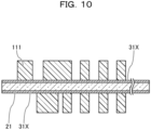
- resist masks 111 are formed on the surfaces of the two TiN layers 31X by a photolithography technique.
- the resist masks 111 cover the portions of the TiN layers 31X that are to form the pads 33, the superconductor layer 32, the superconductor layer 34, the superconductor layer 35, the superconductor layer 36, or the superconductor layer 38.
- etching is performed on the TiN layers 31X, using the resist masks 111. Then, the resist masks 111 are then removed, as illustrated in FIG. 12 . In this manner, the pads 33, the superconductor layer 32, the superconductor layer 34, the superconductor layer 35, the superconductor layer 36, and the superconductor layer 38 are formed.
- a resist mask 112 is formed on the upper surface of the base member 21 by a photolithography technique.
- the resist mask 112 exposes the portions that are to form the quantum bits 23.
- a film 23X to form the quantum bits 23 is formed.
- the film 23X may be formed by a vapor deposition method, for example.
- the resist mask 112 is removed, together with the film 23X formed thereon. That is, lift-off is performed. As a result, the quantum bits 23 are formed.
- protective layers 39 are formed on the upper surface and the lower surface of the base member 21.
- the protective layers 39 SiO 2 layers are formed, for example.
- the protective layers 39 can be formed by a CVD method, for example.
- a resist mask 113 is formed on the protective layer 39 on the upper surface of the base member 21 by a photolithography technique. The resist mask 113 covers the quantum bits 23 from above the protective layer 39.
- etching is performed on the protective layer 39, using the resist mask 113.
- the resist mask 113 is removed.
- resist masks 114 are formed on the upper surface and the lower surface of the base member 21 by a photolithography technique.
- the resist masks 114 expose the portion that is to form the through hole 21A, and the portion that is to form the through hole 21B.
- Deep reactive ion etching (Deep-RIE) is performed on the base member 21, using the resist masks 114.
- the through holes 21A and 21B are formed in the base member 21.
- the resist masks 114 are removed.
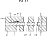
- resist masks 115 are formed on the upper surface and the lower surface of the base member 21 by a photolithography technique.
- the resist masks 115 expose the portion forming the superconductor layer 41, 42, or 43.
- Al layers 42X are formed as superconductor layers.
- the Al layers 42X may be formed by a vapor deposition method, for example.
- the thickness of the Al layers 42X is about 300 nm, for example.
- the resist masks 115 are removed, together with the Al layers 42X formed thereon. That is, lift-off is performed. As a result, the superconductor layers 41, 42, and 43 are formed.
- the superconductor layer 41 is included in the control port 61
- the superconductor layer 42 is included in the read port 62
- the superconductor layer 43 is included in the ground port 63.
- the superconductor layer 42 forms the TSV 72
- the superconductor layer 43 forms the TSV 73.
- a resist mask 116 is formed on the upper surface of the base member 21 by a photolithography technique.
- the resist mask 116 exposes the portions that are to form the first spacers 22.
- an Al layer 22X is formed as the film that is to form the first spacers 22.
- the Al layer 22X may be formed by a vapor deposition method, for example.
- the thickness of the Al layer 22X is about 4 ⁇ m to 6 ⁇ m, for example.
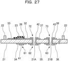
- the resist mask 116 is removed, together with the Al layer 22X formed thereon. That is, lift-off is performed. As a result, the first spacers 22 are formed.
- the quantum bit substrate 20A can be manufactured.
- the quantum bit substrates 20B, 20C, and 20D can also be manufactured by the same method.
- the base member 11 is first prepared, as illustrated in FIG. 29 .
- a silicon substrate can be used, for example.
- the thickness of the base member 11 is about 300 ⁇ m, for example.
- a resist mask 121 is formed on the upper surface of the base member 11 by a photolithography technique.
- the resist mask 121 covers the portions that are to form the protruding portions 13.
- etching is performed on the base member 11 with the use of the resist mask 121, to form the cavities 12.
- the depth of the cavities 12 is set to be about 2 ⁇ m to 4 ⁇ m, for example.
- the protruding portions 13 having a height of about 2 ⁇ m to 4 ⁇ m are formed around the cavities 12.
- the resist mask 121 is removed.
- resist masks 122 are formed on the upper surface and the lower surface of the base member 11 by a photolithography technique.
- the resist masks 122 expose the portions that are to form the through holes 11A.
- resist masks 123 are formed on the upper surface and the lower surface of the base member 11 by a photolithography technique.
- the resist masks 123 expose the portions that are to form the coupler pads 14, the wiring lines 15, and the superconductor layers that join these coupler pads 14 and wiring lines 15.
- Al layers 15X are formed as superconductor layers.
- the Al layers 15X may be formed by a vapor deposition method, for example.
- the resist masks 123 are removed, together with the Al layers 15X formed thereon. That is, lift-off is performed. As a result, the coupler pads 14, the wiring lines 15, and the superconductor layers that join these coupler pads 14 and wiring lines 15 are formed.
- the carrier substrate 10 can be manufactured.
- the quantum bit substrate 20A and the carrier substrate 10 are aligned, the upper surface of the carrier substrate 10 and the lower surface of the quantum bit substrate 20A are made to face each other.
- the first spacers 22 are disposed in the cavities 12. That is, the first spacers 22 are disposed in the regions surrounded by the protruding portions 13.
- the quantum bit substrate 20A is then placed on the carrier substrate 10 while part of the outer surfaces of the first spacers 22 is brought into contact with part of the inner surfaces of the protruding portions 13.
- the lower surfaces of the first spacers 22 are in contact with the upper surface of the base member 11.
- the control probe 51 is pressed against the control port 61
- the read probe 52 is pressed against the read port 62
- the ground probe 53 is pressed against the ground port 63.
- the quantum bit substrate 20A and the carrier substrate 10 can be aligned.
- the alignment between the carrier substrate 10 and the quantum bit substrates 20B, 20C, and 20D can also be performed by a similar method.
- the quantum device 1 according to the first embodiment is completed.
- the first spacers 22 are provided on the lower surface of the base member 21, and thus, a relative positional relationship in the thickness direction between the quantum bit substrate 20A and the carrier substrate 10 is maintained. That is, the distance between the pads 33 and the coupler pads 14 is kept constant. Also, part of the outer surfaces of the first spacers 22 is in contact with part of the inner surfaces of the protruding portions 13. Therefore, the relative position of the quantum bit substrate 20A with respect to the carrier substrate 10 is restricted in a plane parallel to the upper surface of the base member 11. That is, the quantum bit substrate 20A is restricted within a predetermined region that is set beforehand in a plane parallel to the upper surface of the base member 11, by the protruding portions 13 and the first spacers 22.
- the area in which the pads 33 and the coupler pads 14 overlap each other is kept constant in a planar view.
- fluctuations in capacitance between the pads 33 and the coupler pads 14 are reduced.
- the capacitance between the pads 33 and the coupler pads 14 is stabilized.
- the capacitance between the pads 33 and the coupler pads 14 is stabilized in the other quantum bit substrates 20B, 20C, and 20D.
- two coupler pads 14 are coupled via a wiring line 15. Accordingly, the quantum bits 23 included in the quantum bit substrate 20A and the quantum bits 23 included in the quantum bit substrate 20B are capacitively coupled to each other via the wiring lines 15. Likewise, the quantum bits 23 included in the quantum bit substrate 20B and the quantum bits 23 included in the quantum bit substrate 20C are capacitively coupled to each other via the wiring lines 15. The quantum bits 23 included in the quantum bit substrate 20C and the quantum bits 23 included in the quantum bit substrate 20D are capacitively coupled to each other via the wiring lines 15. The quantum bits 23 included in the quantum bit substrate 20D and the quantum bits 23 included in the quantum bit substrate 20A are capacitively coupled to each other via the wiring lines 15.
- the capacitance between the quantum bits can be stabilized, and the number of bits can be increased while a stable capacitance is obtained.
- the pressing by the control probe 51, the read probe 52, and the ground probe 53 is stopped, so that the quantum bit substrates 20A, 20B, 20C, or 20D can be easily removed from the carrier substrate 10.
- the quantum bit substrate can be easily replaced (repaired).
- the ground layer of the quantum bit substrate 20A and the ground layer of the carrier substrate 10 can be electrically coupled via the first spacers 22.
- the quantum bit substrate 20A may not be completely restrained in a plane parallel to the upper surface of the base member 11 by the contact between the protruding portions 13 and the first spacers 22.
- the difference between the distance between the outer rims of the pads 33 and the distance between the outer rims of the coupler pads 14 is preferably larger than the amount by which the quantum bit substrate 20A can move.
- some of the first spacers 22 are located between the pads 33 and the outer rim of the base member 21 in a planar view (see FIG. 3 ). However, as illustrated in FIG. 39 , the first spacers 22 may not be located between the pads 33 and the outer rims of the base member 21.
- the material of the first spacers 22 is not limited to Al, but may be Cu, Au, or the like.
- FIG. 40 is a cross-sectional view illustrating a coupling relationship between two quantum bit substrates in a quantum device according to the second embodiment.
- the protruding portions 13 are formed to be higher than the first spacers 22 of the first embodiment.
- the carrier substrate 10 has second spacers 16 at a plurality of locations inside the cavities 12. That is, the second spacers 16 are provided on the upper surface of the base member 11.
- the height of the second spacers 16 is about the same as the height of the first spacers 22 of the first embodiment, and is 4 ⁇ m to 6 ⁇ m, for example.
- the second spacers 16 continue to the protruding portions 13, for example.
- the second spacers 16 are formed with silicon, for example, and are formed integrally with the base member 11 and the protruding portions 13.
- the second spacers 16 are part of the alignment mechanism.
- the quantum bit substrate 20A does not have the first spacers 22, and part of the outer surface of the base member 21 of the quantum bit substrate 20A is in contact with part of the inner surfaces of the protruding portions 13.
- the upper surfaces of the second spacers 16 are in contact with the lower surface of the base member 21 of the quantum bit substrate 20A.
- the upper surface of the carrier substrate 10 and the lower surface of the quantum bit substrate 20A are made to face each other.
- the quantum bit substrate 20A is then placed on the carrier substrate 10 while part of the outer surface of the base member 21 is brought into contact with part of the inner surfaces of the protruding portions 13.
- the upper surfaces of the second spacers 16 are in contact with the lower surface of the base member 21.
- the second spacers 16 are provided on the upper surface of the base member 11, and thus, a relative positional relationship in the thickness direction between the quantum bit substrate 20A and the carrier substrate 10 is maintained. That is, the distance between the pads 33 and the coupler pads 14 is kept constant. Also, part of the outer surface of the base member 21 is in contact with part of the inner surfaces of the protruding portions 13. Therefore, the relative position of the quantum bit substrate 20A with respect to the carrier substrate 10 is restricted in a plane parallel to the upper surface of the base member 11. Accordingly, the area in which the pads 33 and the coupler pads 14 overlap each other is kept constant in a planar view. Thus, fluctuations in capacitance between the pads 33 and the coupler pads 14 are reduced. In other words, the capacitance between the pads 33 and the coupler pads 14 is stabilized. Likewise, the capacitance between the pads 33 and the coupler pads 14 is stabilized in the other quantum bit substrates 20B, 20C, and 20D.
- the capacitance between the quantum bits can also be stabilized, and the number of bits can also be increased while a stable capacitance is obtained.
- the quantum bit substrate 20A, 20B, 20C, or 20D can be easily removed from the carrier substrate 10, and the quantum bit substrate 20A, 20B, 20C, or 20D can be easily replaced (repaired).
- the first spacers 22 are unnecessary. Thus, contamination and damage due to the formation of the first spacers 22 can be reduced, and more preferable characteristics can be obtained.
- the quantum bit substrate 20A may not be completely restrained in a plane parallel to the upper surface of the base member 11 by the contact between the protruding portions 13 and the base member 21.
- the difference between the distance between the outer rims of the pads 33 and the distance between the outer rims of the coupler pads 14 is preferably larger than the amount by which the quantum bit substrate 20A can move.
Landscapes
- Engineering & Computer Science (AREA)
- General Physics & Mathematics (AREA)
- Theoretical Computer Science (AREA)
- Physics & Mathematics (AREA)
- Mathematical Analysis (AREA)
- Data Mining & Analysis (AREA)
- Evolutionary Computation (AREA)
- Condensed Matter Physics & Semiconductors (AREA)
- Computational Mathematics (AREA)
- Mathematical Optimization (AREA)
- Pure & Applied Mathematics (AREA)
- Computing Systems (AREA)
- General Engineering & Computer Science (AREA)
- Mathematical Physics (AREA)
- Software Systems (AREA)
- Artificial Intelligence (AREA)
- Semiconductor Memories (AREA)
Abstract
Description
- The present disclosure relates to a quantum device and a method for manufacturing the quantum device.
- In quantum computing devices and the like including quantum bits, increasing the number of quantum bits has been considered in preparation for an increase in the amount of calculation.
- In a conventional quantum device, however, it is difficult to stabilize the capacitance between quantum bits in a case where the number of bits is increased.
- An object of the present disclosure is to provide a quantum device capable of stabilizing the capacitance between quantum bits, and a method for manufacturing the quantum device.
- According to an embodiment of the present disclosure, a quantum device is provided, and the quantum device includes: a first substrate; and a plurality of second substrates placed on the first substrate. In the quantum device, the first substrate includes: a first base member that has a first surface; a plurality of first pads provided on the first surface; and a wiring line that couples two first pads of the plurality of first pads, each of the plurality of second substrates includes: a second base member that has a second surface that faces the first surface; a second pad that is provided on the second surface and faces the first pad; and a quantum bit coupled to the second pad, a quantum bit included in one second substrate of the plurality of second substrates and a quantum bit included in another one second substrate of the plurality of second substrates are capacitively coupled to each other via the wiring line. The quantum device includes an alignment mechanism that restrains each of the plurality of second substrates within a predetermined region in a plane parallel to the first surface of the first substrate.
- According to the present disclosure, capacitance between quantum bits can be stabilized.
-
-
FIG. 1 is a top view illustrating a quantum device according to a first embodiment. -
FIG. 2 is a cross-sectional view illustrating the quantum device according to the first embodiment. -
FIG. 3 is a bottom view illustrating a quantum bit substrate included in the quantum device according to the first embodiment. -
FIG. 4 is a schematic diagram illustrating a positional relationship between four quantum bit substrates in the quantum device according to the first embodiment. -
FIG. 5 is a cross-sectional view illustrating a coupling relationship between two quantum bit substrates in the quantum device according to the first embodiment. -
FIG. 6 is a schematic diagram illustrating a coupling relationship between two quantum bit substrates in the quantum device according to the first embodiment. -
FIG. 7 is a partial equivalent circuit diagram of the quantum device according to the first embodiment. -
FIG. 8 is a cross-sectional view illustrating a method for manufacturing a quantum bit substrate (part 1). -
FIG. 9 is a cross-sectional view illustrating the method for manufacturing a quantum bit substrate (part 2). -
FIG. 10 is a cross-sectional view illustrating the method for manufacturing a quantum bit substrate (part 3). -
FIG. 11 is a cross-sectional view illustrating the method for manufacturing a quantum bit substrate (part 4). -
FIG. 12 is a cross-sectional view illustrating the method for manufacturing a quantum bit substrate (part 5). -
FIG. 13 is a cross-sectional view illustrating the method for manufacturing a quantum bit substrate (part 6). -
FIG. 14 is a cross-sectional view illustrating the method for manufacturing a quantum bit substrate (part 7). -
FIG. 15 is a cross-sectional view illustrating the method for manufacturing a quantum bit substrate (part 8). -
FIG. 16 is a cross-sectional view illustrating the method for manufacturing a quantum bit substrate (part 9). -
FIG. 17 is a cross-sectional view illustrating the method for manufacturing a quantum bit substrate (part 10). -
FIG. 18 is a cross-sectional view illustrating the method for manufacturing a quantum bit substrate (part 11). -
FIG. 19 is a cross-sectional view illustrating the method for manufacturing a quantum bit substrate (part 12). -
FIG. 20 is a cross-sectional view illustrating the method for manufacturing a quantum bit substrate (part 13). -
FIG. 21 is a cross-sectional view illustrating the method for manufacturing a quantum bit substrate (part 14). -
FIG. 22 is a cross-sectional view illustrating the method for manufacturing a quantum bit substrate (part 15). -
FIG. 23 is a cross-sectional view illustrating the method for manufacturing a quantum bit substrate (part 16). -
FIG. 24 is a cross-sectional view illustrating the method for manufacturing a quantum bit substrate (part 17). -
FIG. 25 is a cross-sectional view illustrating the method for manufacturing a quantum bit substrate (part 18). -
FIG. 26 is a cross-sectional view illustrating the method for manufacturing a quantum bit substrate (part 19). -
FIG. 27 is a cross-sectional view illustrating the method for manufacturing a quantum bit substrate (part 20). -
FIG. 28 is a cross-sectional view illustrating the method for manufacturing a quantum bit substrate (part 21). -
FIG. 29 is a cross-sectional view illustrating a method for manufacturing a carrier substrate (part 1). -
FIG. 30 is a cross-sectional view illustrating the method for manufacturing a carrier substrate (part 2). -
FIG. 31 is a cross-sectional view illustrating the method for manufacturing a carrier substrate (part 3). -
FIG. 32 is a cross-sectional view illustrating the method for manufacturing a carrier substrate (part 4). -
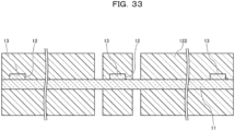
FIG. 33 is a cross-sectional view illustrating the method for manufacturing a carrier substrate (part 5). -
FIG. 34 is a cross-sectional view illustrating the method for manufacturing a carrier substrate (part 6). -
FIG. 35 is a cross-sectional view illustrating the method for manufacturing a carrier substrate (part 7). -
FIG. 36 is a cross-sectional view illustrating the method for manufacturing a carrier substrate (part 8). -
FIG. 37 is a cross-sectional view illustrating the method for manufacturing a carrier substrate (part 9). -
FIG. 38 is a cross-sectional view illustrating the method for manufacturing a carrier substrate (part 10). -
FIG. 39 is a schematic diagram illustrating another example of the layout of first spacers. -
FIG. 40 is a cross-sectional view illustrating a coupling relationship between two quantum bit substrates in a quantum device according to a second embodiment. - In the description below, embodiments of the present disclosure will be specifically explained with reference to the accompanying drawings. Note that, in the present specification and the drawings, components having substantially the same functional configuration are denoted by the same reference signs, and repetitive explanation will not be made.
- First, a first embodiment is described. The first embodiment relates to a quantum device.
FIG. 1 is a top view illustrating the quantum device according to the first embodiment.FIG. 2 is a cross-sectional view illustrating the quantum device according to the first embodiment.FIG. 3 is a bottom view illustrating a quantum bit substrate included in the quantum device according to the first embodiment.FIG. 4 is a schematic diagram illustrating a positional relationship between four quantum bit substrates in the quantum device according to the first embodiment.FIG. 5 is a cross-sectional view illustrating a coupling relationship between two quantum bit substrates in the quantum device according to the first embodiment.FIG. 6 is a schematic diagram illustrating a coupling relationship between two quantum bit substrates in the quantum device according to the first embodiment.FIG. 7 is a partial equivalent circuit diagram of the quantum device according to the first embodiment.FIG. 2 corresponds to a cross-sectional view taken along the line II-II inFIG. 1 .FIG. 5 corresponds to a cross-sectional view taken along the line V-V inFIG. 4 . - As illustrated in
FIG. 1 , aquantum device 1 according to the first embodiment includes acarrier substrate 10, aquantum bit substrate 20A, aquantum bit substrate 20B, aquantum bit substrate 20C, and aquantum bit substrate 20D. Thecarrier substrate 10 is an example of the first substrate, and thequantum bit substrates 20A to 20D are an example of the second substrates. The number of quantum bit substrates is not limited as long as it is two or larger. - As illustrated in
FIG. 2 , thecarrier substrate 10 includes abase member 11, and protrudingportions 13 formed on the upper surface of thebase member 11. Thebase member 11 and the protrudingportions 13 are formed with silicon, for example. Although the details will be described later, fourcavities 12 are formed in a silicon substrate, so that thebase member 11 and the protrudingportions 13 are formed. The protrudingportions 13 are provided at a plurality of locations on the upper surface of thebase member 11, and the protrudingportions 13 provided at the plurality of locations integrally constitute a frame. The height of the protrudingportions 13 is about 2 µm to 4 µm, for example. The upper surface of thebase member 11 is an example of the first surface. The protrudingportions 13 are part of the alignment mechanism. - The
quantum bit substrates 20A to 20D have the same configurations as one another. In the following description of thequantum bit substrates 20A to 20D, only thequantum bit substrate 20A will be explained as a typical example. - The
quantum bit substrate 20A includes abase member 21, and a plurality offirst spacers 22 provided on the lower surface of thebase member 21. As illustrated inFIG. 3 , part of the plurality offirst spacers 22 is formed in the shape of a rectangular frame, and part of the outer surface of eachfirst spacer 22 is in contact with part of the inner surface of a protruding portion 13 (seeFIG. 5 ). As illustrated inFIG. 3 , part of the plurality offirst spacers 22 is provided to have a cross shape, for example, inside afirst spacer 22 formed in the shape of a rectangular frame. The lower surface of eachfirst spacer 22 is in contact with the upper surface of thebase member 11 of thecarrier substrate 10. Eachfirst spacer 22 is an Al layer, for example. The height of thefirst spacers 22 is 4 µm to 6 µm, for example, and is greater than the height of the protrudingportions 13. The lower surface of thebase member 21 is an example of the second surface. Thefirst spacers 22 are part of the alignment mechanism. - As illustrated specifically in
FIGS. 3 to 5 , thequantum bit substrate 20A includes quantum bits (qubits) 23,resonators 24, filters 25,pads 33, acontrol port 61, aread port 62, and aground port 63. - Each
quantum bit 23 is an element that forms a coherent two-level system using superconduction, and has a configuration that includes a transmon quantum bit circuit in which asuperconducting Josephson element 231 and acapacitor 232 are coupled in parallel. Thesuperconducting Josephson element 231 includes a pair of superconductors that exhibit superconductivity at a temperature equal to or lower than a predetermined critical temperature, and an ultrathin insulator that has a thickness of about several nanometers and is sandwiched between the pair of superconductors. The superconductor may be aluminum, for example, and the insulator may be aluminum oxide, for example. - A plurality of
quantum bits 23 is coupled to adjacent otherquantum bits 23 via inter-bit wiring lines 27.Capacitors 28 are provided in the paths of the inter-bit wiring lines 27. With this arrangement, each of thequantum bits 23 creates a quantum entangled state with the adjacent otherquantum bits 23, and performs quantum computing. The intervals between thequantum bits 23 are about 2 mm, for example. As illustrated inFIG. 7 , asuperconducting inductor 236 is coupled between eachquantum bit 23 and the ground.FIG. 7 illustrates only the components in the vicinity of onequantum bit 23. - The
resonators 24 interact with thequantum bits 23, to read bit signals indicating the states of thequantum bits 23. Theresonators 24 are coupled to thequantum bits 23 viacapacitors 233. Eachresonator 24 includes a resonance circuit in which asuperconducting inductor 241 and acapacitor 242 are coupled in parallel. - The
filters 25 are coupled to theresonators 24 viacapacitors 243. Eachfilter 25 includes a circuit in which asuperconducting inductor 251 and acapacitor 252 are coupled in parallel. - The
pads 33 are coupled to some of thequantum bits 23, and are used for coupling toquantum bits 23 provided on thequantum bit substrate pads 33 have a square planar shape, with a side length of about 200 µm, for example. Thepads 33 are an example of the second pads. The distance between thepads 33 and thefirst spacer 22 is about 100 µm to 200 µm, for example. This is to avoid coupling between thepads 33 and thefirst spacer 22. - For example, four sets of
resonators 24 andquantum bits 23 are coupled to eachfilter 25. Thequantum bits 23, theresonators 24, thefilters 25, and thepads 33 are provided on the lower surface of thebase member 21. - The
control port 61, the readport 62, and theground port 63 are access ports for accessing a quantum computing circuit including thequantum bits 23, theresonators 24, and thefilters 25, from the outside. Thecontrol port 61, the readport 62, and theground port 63 are provided on the upper surface of thebase member 21. - The
control port 61 is coupled to eachquantum bit 23 via acapacitor 234. Thecontrol port 61 is used to control thequantum bits 23 from the outside. Asuperconducting inductor 235 is coupled between the ground and the wiring line between thecontrol port 61 and thecapacitor 234. - The read
port 62 is coupled to eachfilter 25 via a through silicon via (TSV) 72 provided on thebase member 21 and acapacitor 253. The readport 62 is used to extract bit signals read by theresonators 24 to the outside. - The
ground port 63 is coupled to thequantum bits 23, theresonators 24, and thefilters 25 via theTSV 73. Theground port 63 is used to apply a ground potential to thequantum bits 23, theresonator 24, and thefilters 25, from the outside. - As illustrated in
FIG. 5 , throughholes base member 21. - The
pads 33, thequantum bits 23, asuperconductor layer 32, and asuperconductor layer 38 are provided on the lower surface of thebase member 21. Thepads 33 and thequantum bits 23 are coupled to each other. Thesuperconductor layer 32 forms theresonators 24 and thefilters 25, and is coupled to thequantum bits 23. Thesuperconductor layer 32 is adjacent to the throughhole 21A. Thesuperconductor layer 38 is adjacent to the throughhole 21B. Thepads 33, thesuperconductor layer 32, and thesuperconductor layer 38 are TiN layers, for example. The thicknesses of thepads 33, thesuperconductor layer 32, and thesuperconductor layer 38 are about 100 nm, for example. - A
superconductor layer 34, asuperconductor layer 35, and asuperconductor layer 36 are provided on the upper surface of thebase member 21. Thesuperconductor layer 34 overlaps thequantum bits 23 in a planar view. Thesuperconductor layer 35 is adjacent to the throughhole 21A, and is included in theTSV 72. Thesuperconductor layer 36 is adjacent to the throughhole 21B, and is included in theTSV 73. Thesuperconductor layer 34, thesuperconductor layer 35, and thesuperconductor layer 36 are TiN layers, for example. The thicknesses of thesuperconductor layer 34, thesuperconductor layer 35, and thesuperconductor layer 36 are about 100 nm, for example. - A
superconductor layer 41 is provided on thesuperconductor layer 34, asuperconductor layer 42 is provided inside the throughhole 21A, and asuperconductor layer 43 is provided inside the throughhole 21B. Thesuperconductor layer 42 is in contact with the superconductor layers 32 and 35. Thesuperconductor layer 43 is in contact with the superconductor layers 36 and 38. Thesuperconductor layer 42 forms theTSV 72, and thesuperconductor layer 43 forms theTSV 73. The superconductor layers 41, 42, and 43 are Al layers, for example. The thicknesses of the superconductor layers 41, 42, and 43 is about 300 nm, for example. Thesuperconductor layer 41 is included in thecontrol port 61, thesuperconductor layer 42 is included in the readport 62, and thesuperconductor layer 43 is included in theground port 63. - As illustrated in
FIGS. 5 and6 , throughholes 11A are formed in thebase member 11 of thecarrier substrate 10 so as to correspond to thepads 33. The throughholes 11A each have a circular planar shape with a diameter of about 150 µm, for example. Further, acoupler pad 14 is provided on the upper surface of thebase member 11 around each throughhole 11A. The outer rim of eachcoupler pad 14 has a circular planar shape with a diameter of about 180 µm, for example. Thecoupler pads 14 are an example of the first pads. Superconductor layers that continue to thecoupler pads 14 are provided inside the throughholes 11A. Awiring line 15 is provided on the lower surface of thebase member 11. Thewiring line 15 continues to the superconductor layers inside two throughholes 11A. Accordingly, twocoupler pads 14 are coupled to each other via thewiring line 15. The twocoupler pads 14 coupled via thewiring line 15 correspond to different quantum bit substrates from each other. In the example illustrated inFIG. 5 , one of thecoupler pads 14 corresponds to thequantum bit substrate 20A, and theother coupler pad 14 corresponds to thequantum bit substrate 20B. - The
coupler pads 14 face thepads 33, with a distance being maintained from thepads 33. Apad 33 and acoupler pad 14 can function as two electrodes included in one capacitance. In a planar view, thepads 33 have a rectangular shape, and thecoupler pads 14 have an annular shape. Thecoupler pads 14 may be circular. In a planar view, the outer rim of eachcoupler pad 14 is located on the inner side of the outer rim of thepad 33. - A
control probe 51, aread probe 52, and aground probe 53 are pressed against the upper surface of thequantum bit substrate 20A. Thecontrol probe 51 is pressed against thecontrol port 61, theread probe 52 is pressed against the readport 62, and theground probe 53 is pressed against theground port 63. - Next, a method for manufacturing the
quantum device 1 according to the first embodiment is described. Here, a method for manufacturing thequantum bit substrate 20A, a method for manufacturing thecarrier substrate 10, and a method for aligning thequantum bit substrate 20A and thecarrier substrate 10 are sequentially described.FIGS. 8 to 28 are cross-sectional views illustrating the method for manufacturing thequantum bit substrate 20A, andFIGS. 29 to 38 are cross-sectional views illustrating the method for manufacturing thecarrier substrate 10. In the description of the method for manufacturing thequantum bit substrate 20A, thequantum device 1 is turned upside down, for convenience sake. - In the manufacturing of the
quantum bit substrate 20A, thebase member 21 is first prepared, as illustrated inFIG. 8 . As thebase member 21, a silicon substrate can be used, for example. The thickness of thebase member 21 is about 300 µm, for example. - Next, as illustrated in
FIG. 9 , superconductor layers such as TiN layers 31X, for example, are formed on the upper surface and the lower surface of thebase member 21. The TiN layers 31X can be formed by a sputtering method, a plasma chemical vapor deposition (CVD) method, an ion plating method, or the like, for example. The thickness of the TiN layers 31X is about 100 nm, for example. - After that, as illustrated in
FIG. 10 , resistmasks 111 are formed on the surfaces of the twoTiN layers 31X by a photolithography technique. The resistmasks 111 cover the portions of the TiN layers 31X that are to form thepads 33, thesuperconductor layer 32, thesuperconductor layer 34, thesuperconductor layer 35, thesuperconductor layer 36, or thesuperconductor layer 38. - Subsequently, as illustrated in
FIG. 11 , etching is performed on the TiN layers 31X, using the resist masks 111. Then, the resistmasks 111 are then removed, as illustrated inFIG. 12 . In this manner, thepads 33, thesuperconductor layer 32, thesuperconductor layer 34, thesuperconductor layer 35, thesuperconductor layer 36, and thesuperconductor layer 38 are formed. - Next, as illustrated in
FIG. 13 , a resistmask 112 is formed on the upper surface of thebase member 21 by a photolithography technique. The resistmask 112 exposes the portions that are to form thequantum bits 23. - After that, as illustrated in
FIG. 14 , afilm 23X to form thequantum bits 23 is formed. Thefilm 23X may be formed by a vapor deposition method, for example. - Subsequently, as illustrated in
FIG. 15 , the resistmask 112 is removed, together with thefilm 23X formed thereon. That is, lift-off is performed. As a result, thequantum bits 23 are formed. - Next, as illustrated in
FIG. 16 ,protective layers 39 are formed on the upper surface and the lower surface of thebase member 21. As theprotective layers 39, SiO2 layers are formed, for example. The protective layers 39 can be formed by a CVD method, for example. Further, a resistmask 113 is formed on theprotective layer 39 on the upper surface of thebase member 21 by a photolithography technique. The resistmask 113 covers thequantum bits 23 from above theprotective layer 39. - After that, as illustrated in
FIG. 17 , etching is performed on theprotective layer 39, using the resistmask 113. Subsequently, as illustrated inFIG. 18 , the resistmask 113 is removed. - Next, as illustrated in
FIG. 19 , resistmasks 114 are formed on the upper surface and the lower surface of thebase member 21 by a photolithography technique. The resistmasks 114 expose the portion that is to form the throughhole 21A, and the portion that is to form the throughhole 21B. - After that, as illustrated in
FIG. 20 , deep reactive ion etching (Deep-RIE) is performed on thebase member 21, using the resist masks 114. As a result, the throughholes base member 21. Subsequently, as illustrated inFIG. 21 , the resistmasks 114 are removed. - Next, as illustrated in
FIG. 22 , resistmasks 115 are formed on the upper surface and the lower surface of thebase member 21 by a photolithography technique. The resistmasks 115 expose the portion forming thesuperconductor layer - After that, as illustrated in
FIG. 23 , Al layers 42X are formed as superconductor layers. The Al layers 42X may be formed by a vapor deposition method, for example. The thickness of the Al layers 42X is about 300 nm, for example. - Subsequently, as illustrated in
FIG. 24 , the resistmasks 115 are removed, together with the Al layers 42X formed thereon. That is, lift-off is performed. As a result, the superconductor layers 41, 42, and 43 are formed. Thesuperconductor layer 41 is included in thecontrol port 61, thesuperconductor layer 42 is included in the readport 62, and thesuperconductor layer 43 is included in theground port 63. Further, thesuperconductor layer 42 forms theTSV 72, and thesuperconductor layer 43 forms theTSV 73. - Next, as illustrated in
FIG. 25 , a resistmask 116 is formed on the upper surface of thebase member 21 by a photolithography technique. The resistmask 116 exposes the portions that are to form thefirst spacers 22. - After that, as illustrated in
FIG. 26 , anAl layer 22X is formed as the film that is to form thefirst spacers 22. TheAl layer 22X may be formed by a vapor deposition method, for example. The thickness of theAl layer 22X is about 4 µm to 6 µm, for example. - Subsequently, as illustrated in
FIG. 27 , the resistmask 116 is removed, together with theAl layer 22X formed thereon. That is, lift-off is performed. As a result, thefirst spacers 22 are formed. - Next, as illustrated in
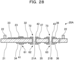
FIG. 28 , theprotective layers 39 are removed. - In this manner, the
quantum bit substrate 20A can be manufactured. Thequantum bit substrates - In the manufacturing of the
carrier substrate 10, thebase member 11 is first prepared, as illustrated inFIG. 29 . As thebase member 11, a silicon substrate can be used, for example. The thickness of thebase member 11 is about 300 µm, for example. - Next, as illustrated in
FIG. 30 , a resistmask 121 is formed on the upper surface of thebase member 11 by a photolithography technique. The resistmask 121 covers the portions that are to form the protrudingportions 13. - After that, as illustrated in
FIG. 31 , etching is performed on thebase member 11 with the use of the resistmask 121, to form thecavities 12. The depth of thecavities 12 is set to be about 2 µm to 4 µm, for example. As a result, the protrudingportions 13 having a height of about 2 µm to 4 µm are formed around thecavities 12. Subsequently, as illustrated inFIG. 32 , the resistmask 121 is removed. - Next, as illustrated in
FIG. 33 , resistmasks 122 are formed on the upper surface and the lower surface of thebase member 11 by a photolithography technique. The resistmasks 122 expose the portions that are to form the throughholes 11A. - After that, as illustrated in
FIG. 34 , Deep-RIE is performed on thebase member 11, using the resist masks 122. As a result, the throughholes 11A are formed in thebase member 11. Subsequently, as illustrated inFIG. 35 , the resistmasks 122 are removed. - Next, as illustrated in
FIG. 36 , resistmasks 123 are formed on the upper surface and the lower surface of thebase member 11 by a photolithography technique. The resistmasks 123 expose the portions that are to form thecoupler pads 14, thewiring lines 15, and the superconductor layers that join thesecoupler pads 14 and wiring lines 15. - After that, as illustrated in
FIG. 37 , Al layers 15X are formed as superconductor layers. The Al layers 15X may be formed by a vapor deposition method, for example. - Subsequently, as illustrated in
FIG. 38 , the resistmasks 123 are removed, together with the Al layers 15X formed thereon. That is, lift-off is performed. As a result, thecoupler pads 14, thewiring lines 15, and the superconductor layers that join thesecoupler pads 14 andwiring lines 15 are formed. - In this manner, the
carrier substrate 10 can be manufactured. - When the
quantum bit substrate 20A and thecarrier substrate 10 are aligned, the upper surface of thecarrier substrate 10 and the lower surface of thequantum bit substrate 20A are made to face each other. Next, thefirst spacers 22 are disposed in thecavities 12. That is, thefirst spacers 22 are disposed in the regions surrounded by the protrudingportions 13. Then, thequantum bit substrate 20A is then placed on thecarrier substrate 10 while part of the outer surfaces of thefirst spacers 22 is brought into contact with part of the inner surfaces of the protrudingportions 13. As a result, the lower surfaces of thefirst spacers 22 are in contact with the upper surface of thebase member 11. After that, thecontrol probe 51 is pressed against thecontrol port 61, theread probe 52 is pressed against the readport 62, and theground probe 53 is pressed against theground port 63. - In this manner, the
quantum bit substrate 20A and thecarrier substrate 10 can be aligned. The alignment between thecarrier substrate 10 and thequantum bit substrates - In this manner, the
quantum device 1 according to the first embodiment is completed. - In the first embodiment, the
first spacers 22 are provided on the lower surface of thebase member 21, and thus, a relative positional relationship in the thickness direction between thequantum bit substrate 20A and thecarrier substrate 10 is maintained. That is, the distance between thepads 33 and thecoupler pads 14 is kept constant. Also, part of the outer surfaces of thefirst spacers 22 is in contact with part of the inner surfaces of the protrudingportions 13. Therefore, the relative position of thequantum bit substrate 20A with respect to thecarrier substrate 10 is restricted in a plane parallel to the upper surface of thebase member 11. That is, thequantum bit substrate 20A is restricted within a predetermined region that is set beforehand in a plane parallel to the upper surface of thebase member 11, by the protrudingportions 13 and thefirst spacers 22. Accordingly, the area in which thepads 33 and thecoupler pads 14 overlap each other is kept constant in a planar view. Thus, fluctuations in capacitance between thepads 33 and thecoupler pads 14 are reduced. In other words, the capacitance between thepads 33 and thecoupler pads 14 is stabilized. Likewise, the capacitance between thepads 33 and thecoupler pads 14 is stabilized in the otherquantum bit substrates - In the present embodiment, on the
carrier substrate 10, twocoupler pads 14 are coupled via awiring line 15. Accordingly, thequantum bits 23 included in thequantum bit substrate 20A and thequantum bits 23 included in thequantum bit substrate 20B are capacitively coupled to each other via the wiring lines 15. Likewise, thequantum bits 23 included in thequantum bit substrate 20B and thequantum bits 23 included in thequantum bit substrate 20C are capacitively coupled to each other via the wiring lines 15. Thequantum bits 23 included in thequantum bit substrate 20C and thequantum bits 23 included in thequantum bit substrate 20D are capacitively coupled to each other via the wiring lines 15. Thequantum bits 23 included in thequantum bit substrate 20D and thequantum bits 23 included in thequantum bit substrate 20A are capacitively coupled to each other via the wiring lines 15. - Thus, according to the first embodiment, the capacitance between the quantum bits can be stabilized, and the number of bits can be increased while a stable capacitance is obtained.
- Further, the pressing by the
control probe 51, theread probe 52, and theground probe 53 is stopped, so that thequantum bit substrates carrier substrate 10. Thus, even in a case where an operation failure or the like occurs in any of thequantum bit substrates - Further, in a case where the
first spacers 22 are Al layers, the ground layer of thequantum bit substrate 20A and the ground layer of thecarrier substrate 10 can be electrically coupled via thefirst spacers 22. - Note that the
quantum bit substrate 20A may not be completely restrained in a plane parallel to the upper surface of thebase member 11 by the contact between the protrudingportions 13 and thefirst spacers 22. For example, there may be a distance between the protrudingportions 13 and thefirst spacers 22 so that thequantum bit substrate 20A can be easily placed on thecarrier substrate 10. In this case, in each direction in the plane parallel to the upper surface of thebase member 11, the difference between the distance between the outer rims of thepads 33 and the distance between the outer rims of thecoupler pads 14 is preferably larger than the amount by which thequantum bit substrate 20A can move. With such a configuration, even if thequantum bit substrate 20A moves in the plane, the area where thepads 33 and thecoupler pads 14 overlap each other in a planar view is kept constant, and a stable capacitance can be obtained. - Further, in the
quantum bit substrate 20A included in the first embodiment, some of thefirst spacers 22 are located between thepads 33 and the outer rim of thebase member 21 in a planar view (seeFIG. 3 ). However, as illustrated inFIG. 39 , thefirst spacers 22 may not be located between thepads 33 and the outer rims of thebase member 21. - Furthermore, the material of the
first spacers 22 is not limited to Al, but may be Cu, Au, or the like. - Next, a second embodiment is described. The second embodiment differs from the first embodiment mainly in the configuration of the alignment mechanism.
FIG. 40 is a cross-sectional view illustrating a coupling relationship between two quantum bit substrates in a quantum device according to the second embodiment. - In the second embodiment, the protruding
portions 13 are formed to be higher than thefirst spacers 22 of the first embodiment. Further, thecarrier substrate 10 has second spacers 16 at a plurality of locations inside thecavities 12. That is, thesecond spacers 16 are provided on the upper surface of thebase member 11. The height of thesecond spacers 16 is about the same as the height of thefirst spacers 22 of the first embodiment, and is 4 µm to 6 µm, for example. Thesecond spacers 16 continue to the protrudingportions 13, for example. Thesecond spacers 16 are formed with silicon, for example, and are formed integrally with thebase member 11 and the protrudingportions 13. Thesecond spacers 16 are part of the alignment mechanism. - Further, in the present embodiment, the
quantum bit substrate 20A does not have thefirst spacers 22, and part of the outer surface of thebase member 21 of thequantum bit substrate 20A is in contact with part of the inner surfaces of the protrudingportions 13. The upper surfaces of thesecond spacers 16 are in contact with the lower surface of thebase member 21 of thequantum bit substrate 20A. - Other components are the same as those of the first embodiment.
- In the second embodiment, when the
quantum bit substrate 20A and thecarrier substrate 10 are aligned, the upper surface of thecarrier substrate 10 and the lower surface of thequantum bit substrate 20A are made to face each other. Thequantum bit substrate 20A is then placed on thecarrier substrate 10 while part of the outer surface of thebase member 21 is brought into contact with part of the inner surfaces of the protrudingportions 13. As a result, the upper surfaces of thesecond spacers 16 are in contact with the lower surface of thebase member 21. After that, thecontrol probe 51 is pressed against thecontrol port 61, theread probe 52 is pressed against the readport 62, and theground probe 53 is pressed against theground port 63. - In the second embodiment, the
second spacers 16 are provided on the upper surface of thebase member 11, and thus, a relative positional relationship in the thickness direction between thequantum bit substrate 20A and thecarrier substrate 10 is maintained. That is, the distance between thepads 33 and thecoupler pads 14 is kept constant. Also, part of the outer surface of thebase member 21 is in contact with part of the inner surfaces of the protrudingportions 13. Therefore, the relative position of thequantum bit substrate 20A with respect to thecarrier substrate 10 is restricted in a plane parallel to the upper surface of thebase member 11. Accordingly, the area in which thepads 33 and thecoupler pads 14 overlap each other is kept constant in a planar view. Thus, fluctuations in capacitance between thepads 33 and thecoupler pads 14 are reduced. In other words, the capacitance between thepads 33 and thecoupler pads 14 is stabilized. Likewise, the capacitance between thepads 33 and thecoupler pads 14 is stabilized in the otherquantum bit substrates - Thus, according to the second embodiment, the capacitance between the quantum bits can also be stabilized, and the number of bits can also be increased while a stable capacitance is obtained.
- Also, as in the first embodiment, the
quantum bit substrate carrier substrate 10, and thequantum bit substrate - Further, in the second embodiment, the
first spacers 22 are unnecessary. Thus, contamination and damage due to the formation of thefirst spacers 22 can be reduced, and more preferable characteristics can be obtained. - Note that the
quantum bit substrate 20A may not be completely restrained in a plane parallel to the upper surface of thebase member 11 by the contact between the protrudingportions 13 and thebase member 21. For example, there may be a distance between the protrudingportions 13 and thebase member 21 so that thequantum bit substrate 20A can be easily placed on thecarrier substrate 10. In this case, in each direction in the plane parallel to the upper surface of thebase member 11, the difference between the distance between the outer rims of thepads 33 and the distance between the outer rims of thecoupler pads 14 is preferably larger than the amount by which thequantum bit substrate 20A can move. With such a configuration, even if thequantum bit substrate 20A moves in the plane, the area where thepads 33 and thecoupler pads 14 overlap each other in a planar view is kept constant, and a stable capacitance can be obtained. - Although the preferred embodiments and the like have been described in detail so far, the present disclosure is not limited to the embodiments and the like described above, and various modifications and substitutions may be made to the embodiments and the like described above, without departing from the scope disclosed in the claims.
-
- Patent Document 1:
U.S. Patent Application Publication No. 2018/0013052 - Patent Document 2:
U.S. Patent Application Publication No. 2019/0042964 - Patent Document 3:
Japanese Laid-open Patent Publication No. 2021-72351 - Patent Document 4:
Japanese Laid-open Patent Publication No. 2020-61554 -
- 1Quantum device
- 10Carrier substrate
- 11Base member
- 12Cavity
- 13Protruding portion
- 14Coupler pad
- 15Wiring line
- 16Second spacer
- 20A, 20B, 20C, 20DQuantum bit substrate
- 21Base member
- 21A, 21BThrough hole
- 22First spacer
- 23Quantum bit
- 24Resonator
- 25Filter
- 33Pad
- 51Control probe
- 52Read probe
- 53Ground probe
- 61Control port
- 62Read port
- 63Ground port
Claims (10)
- A quantum device comprising:a first substrate; anda plurality of second substrates placed on the first substrate, whereinthe first substrate includes:a first base member that has a first surface;a plurality of first pads provided on the first surface; anda wiring line that couples two first pads of the plurality of first pads,each of the plurality of second substrates includes:a second base member that has a second surface that faces the first surface;a second pad that is provided on the second surface, and faces the first pad; anda quantum bit coupled to the second pad,a quantum bit included in one second substrate of the plurality of second substrates and a quantum bit included in another one second substrate of the plurality of second substrates are capacitively coupled to each other via the wiring line, andthe quantum device comprises an alignment mechanism that restrains each of the plurality of second substrates within a predetermined region in a plane parallel to the first surface of the first substrate.
- The quantum device according to claim 1, whereinthe alignment mechanism includes protruding portions provided at a plurality of locations on the first surface, andthe protruding portions restrain each of the plurality of second substrates within the predetermined region.
- The quantum device according to claim 1 or 2, further comprising first spacers that are provided at a plurality of locations on the second surface, and are in contact with the first surface.
- The quantum device according to claim 1, wherein
the alignment mechanism includes:protruding portions provided at a plurality of locations on the first surface; andfirst spacers that are provided at a plurality of locations on the second surface, and are in contact with the first surface and the protruding portions, andthe protruding portions restrain each of the plurality of second substrates within the predetermined region. - The quantum device according to claim 1 or 2, further comprising second spacers that are provided at a plurality of locations on the first surface, and are in contact with the second surface.
- The quantum device according to claim 1, wherein
the alignment mechanism includes:protruding portions provided at a plurality of locations on the first surface; andsecond spacers that are provided at a plurality of locations on the first surface, and are in contact with the second surface, andthe second base member is in contact with the protruding portions. - The quantum device according to claim 6, wherein the second spacers continue to the protruding portions.
- The quantum device according to any one of claims 1 to 7, wherein, in each direction in the plane parallel to the first surface,
a difference between a distance between outer rims of the second pads and a distance between outer edges of the first pads is larger than a movable amount of each of the plurality of second substrates. - The quantum device according to any one of claims 1 to 8, wherein the wiring line is provided on an opposite surface of the first base member from the first surface.
- A method for manufacturing a quantum device, the method comprising:a process of preparing a first substrate that includes a first base member that has a first surface, a plurality of first pads provided on the first surface, and a wiring line that couples two first pads of the plurality of first pads;a process of preparing a plurality of second substrates that include a second base member that has a second surface, a second pad that is provided on the second surface and faces the first pads, and a quantum bit coupled to the second pad; anda process of placing each of the plurality of second substrates on the first substrate, while causing the second surface to face the first surface, whereina quantum bit included in one second substrate of the plurality of second substrates and a quantum bit included in another one second substrate of the plurality of second substrates are capacitively coupled to each other via the wiring line, andan alignment mechanism restrains each of the plurality of second substrates within a predetermined region in a plane parallel to the first surface of the first substrate.
Applications Claiming Priority (1)
| Application Number | Priority Date | Filing Date | Title |
|---|---|---|---|
| PCT/JP2022/016879 WO2023188391A1 (en) | 2022-03-31 | 2022-03-31 | Quantum device and method for manufacturing quantum device |
Publications (2)
| Publication Number | Publication Date |
|---|---|
| EP4503904A1 true EP4503904A1 (en) | 2025-02-05 |
| EP4503904A4 EP4503904A4 (en) | 2025-05-28 |
Family
ID=88200428
Family Applications (1)
| Application Number | Title | Priority Date | Filing Date |
|---|---|---|---|
| EP22935529.2A Pending EP4503904A4 (en) | 2022-03-31 | 2022-03-31 | QUANTUM DEVICE AND METHOD FOR MANUFACTURING QUANTUM DEVICE |
Country Status (3)
| Country | Link |
|---|---|
| EP (1) | EP4503904A4 (en) |
| JP (1) | JP7819759B2 (en) |
| WO (1) | WO2023188391A1 (en) |
Families Citing this family (6)
| Publication number | Priority date | Publication date | Assignee | Title |
|---|---|---|---|---|
| WO2025069381A1 (en) * | 2023-09-29 | 2025-04-03 | 富士通株式会社 | Quantum device |
| WO2025134388A1 (en) * | 2023-12-22 | 2025-06-26 | Riken | Fabrication method for electric circuit device, and qubit device |
| JP2025112080A (en) * | 2024-01-18 | 2025-07-31 | 富士通株式会社 | Manufacturing method for quantum bit device |
| WO2025211421A1 (en) * | 2024-04-03 | 2025-10-09 | 京セラ株式会社 | Structure, quantum processor, quantum computer, and method for manufacturing structure |
| WO2025216276A1 (en) * | 2024-04-11 | 2025-10-16 | 京セラ株式会社 | Structure, quantum processor, quantum computer, and method for manufacturing structure |
| JP2026051845A (en) | 2024-09-10 | 2026-03-23 | 富士通株式会社 | Qubit device and method for manufacturing a qubit device |
Family Cites Families (7)
| Publication number | Priority date | Publication date | Assignee | Title |
|---|---|---|---|---|
| US10134972B2 (en) | 2015-07-23 | 2018-11-20 | Massachusetts Institute Of Technology | Qubit and coupler circuit structures and coupling techniques |
| CN118133978A (en) * | 2017-03-13 | 2024-06-04 | 谷歌有限责任公司 | Integrated circuit components in a stacked quantum computing device |
| US10263170B1 (en) * | 2017-11-30 | 2019-04-16 | International Business Machines Corporation | Bumped resonator structure |
| US10380496B2 (en) | 2018-03-19 | 2019-08-13 | Intel Corporation | Quantum computing assemblies |
| US11088310B2 (en) | 2019-04-29 | 2021-08-10 | International Business Machines Corporation | Through-silicon-via fabrication in planar quantum devices |
| JP7427914B2 (en) | 2019-10-30 | 2024-02-06 | 日本電気株式会社 | Superconducting circuit device, spacer, and method for manufacturing superconducting circuit device |
| JP7133854B2 (en) | 2019-10-31 | 2022-09-09 | 国立研究開発法人科学技術振興機構 | Superconducting composite quantum computing circuit |
-
2022
- 2022-03-31 JP JP2024511130A patent/JP7819759B2/en active Active
- 2022-03-31 WO PCT/JP2022/016879 patent/WO2023188391A1/en not_active Ceased
- 2022-03-31 EP EP22935529.2A patent/EP4503904A4/en active Pending
Also Published As
| Publication number | Publication date |
|---|---|
| JP7819759B2 (en) | 2026-02-25 |
| WO2023188391A1 (en) | 2023-10-05 |
| EP4503904A4 (en) | 2025-05-28 |
| JPWO2023188391A1 (en) | 2023-10-05 |
Similar Documents
| Publication | Publication Date | Title |
|---|---|---|
| JP7819759B2 (en) | Quantum device and method for manufacturing the same | |
| JP7608655B2 (en) | Pillars as stoppers for precise chip-to-chip isolation | |
| US12518977B2 (en) | Signal distribution for a quantum computing system | |
| EP3580702B1 (en) | Integrating circuit elements in a stacked quantum computing device | |
| US12086689B1 (en) | Scalable quantum processor design | |
| KR100354296B1 (en) | Semiconductor Storage Device And Method For Fabricating The Same | |
| US10319896B2 (en) | Shielded interconnects | |
| WO2018160187A1 (en) | Superconducting qubit devices with hexagonal boron nitride josephson junctions | |
| US20260082822A1 (en) | Quantum operation device and method of manufacturing quantum operation device | |
| CN116458007A (en) | Embedded microstrip transmission line | |
| JPH02265243A (en) | Multilayer wiring and its formation | |
| CN112701083B (en) | Method of forming pattern | |
| EP4408151B1 (en) | Qubit chip device and method of manufacturing the same | |
| EP4730215A2 (en) | Method for manufacturing quantum computing apparatus | |
| WO2024224493A1 (en) | Quantum computing device and method for manufacturing quantum computing device | |
| CN218456648U (en) | Electrode, josephson junction, superconducting quantum device and chip | |
| CN117568745A (en) | Hard mask and its preparation methods and applications, Josephson junction and related preparation methods | |
| EP4709128A1 (en) | Quantum bit device and method for manufacturing quantum bit device | |
| EP4709129A1 (en) | Quantum bit device and method for manufacturing quantum bit device | |
| EP4626213A1 (en) | Device and manufacturing method for device | |
| EP4712751A1 (en) | Qubit device and method of manufacturing qubit device | |
| CN221354899U (en) | Josephson junction device and superconducting quantum chip | |
| US20250359488A1 (en) | Fabrication of superconducting tunnel junctions | |
| KR20250112631A (en) | Air bridge type superconducting coupler and superconducting computing apparatus including the same | |
| KR20240117866A (en) | Josephson junction device, superconducting qubit including the Josephson junction device, and method for manufacturing the Josephson junction device |
Legal Events
| Date | Code | Title | Description |
|---|---|---|---|
| STAA | Information on the status of an ep patent application or granted ep patent |
Free format text: STATUS: THE INTERNATIONAL PUBLICATION HAS BEEN MADE |
|
| PUAI | Public reference made under article 153(3) epc to a published international application that has entered the european phase |
Free format text: ORIGINAL CODE: 0009012 |
|
| STAA | Information on the status of an ep patent application or granted ep patent |
Free format text: STATUS: REQUEST FOR EXAMINATION WAS MADE |
|
| 17P | Request for examination filed |
Effective date: 20240905 |
|
| AK | Designated contracting states |
Kind code of ref document: A1 Designated state(s): AL AT BE BG CH CY CZ DE DK EE ES FI FR GB GR HR HU IE IS IT LI LT LU LV MC MK MT NL NO PL PT RO RS SE SI SK SM TR |
|
| REG | Reference to a national code |
Ref country code: DE Ref legal event code: R079 Free format text: PREVIOUS MAIN CLASS: H10N0060100000 Ipc: G06N0010400000 |
|
| A4 | Supplementary search report drawn up and despatched |
Effective date: 20250428 |
|
| RIC1 | Information provided on ipc code assigned before grant |
Ipc: H10N 69/00 20230101ALN20250422BHEP Ipc: H10N 60/01 20230101ALI20250422BHEP Ipc: H10N 60/80 20230101ALI20250422BHEP Ipc: H10N 60/10 20230101ALI20250422BHEP Ipc: G06N 10/40 20220101AFI20250422BHEP |
|
| DAV | Request for validation of the european patent (deleted) | ||
| DAX | Request for extension of the european patent (deleted) |