EP4503903A1 - Superconducting quantum circuit - Google Patents
Superconducting quantum circuit Download PDFInfo
- Publication number
- EP4503903A1 EP4503903A1 EP22935189.5A EP22935189A EP4503903A1 EP 4503903 A1 EP4503903 A1 EP 4503903A1 EP 22935189 A EP22935189 A EP 22935189A EP 4503903 A1 EP4503903 A1 EP 4503903A1
- Authority
- EP
- European Patent Office
- Prior art keywords
- coupler
- qubits
- superconducting
- electrode
- capacitance
- Prior art date
- Legal status (The legal status is an assumption and is not a legal conclusion. Google has not performed a legal analysis and makes no representation as to the accuracy of the status listed.)
- Granted
Links
Images


Classifications
-
- H—ELECTRICITY
- H10—SEMICONDUCTOR DEVICES; ELECTRIC SOLID-STATE DEVICES NOT OTHERWISE PROVIDED FOR
- H10N—ELECTRIC SOLID-STATE DEVICES NOT OTHERWISE PROVIDED FOR
- H10N69/00—Integrated devices, or assemblies of multiple devices, comprising at least one superconducting element covered by group H10N60/00
-
- G—PHYSICS
- G06—COMPUTING OR CALCULATING; COUNTING
- G06N—COMPUTING ARRANGEMENTS BASED ON SPECIFIC COMPUTATIONAL MODELS
- G06N10/00—Quantum computing, i.e. information processing based on quantum-mechanical phenomena
- G06N10/20—Models of quantum computing, e.g. quantum circuits or universal quantum computers
-
- G—PHYSICS
- G06—COMPUTING OR CALCULATING; COUNTING
- G06N—COMPUTING ARRANGEMENTS BASED ON SPECIFIC COMPUTATIONAL MODELS
- G06N10/00—Quantum computing, i.e. information processing based on quantum-mechanical phenomena
- G06N10/40—Physical realisations or architectures of quantum processors or components for manipulating qubits, e.g. qubit coupling or qubit control
-
- H—ELECTRICITY
- H10—SEMICONDUCTOR DEVICES; ELECTRIC SOLID-STATE DEVICES NOT OTHERWISE PROVIDED FOR
- H10N—ELECTRIC SOLID-STATE DEVICES NOT OTHERWISE PROVIDED FOR
- H10N60/00—Superconducting devices
- H10N60/10—Junction-based devices
- H10N60/12—Josephson-effect devices
-
- H—ELECTRICITY
- H10—SEMICONDUCTOR DEVICES; ELECTRIC SOLID-STATE DEVICES NOT OTHERWISE PROVIDED FOR
- H10N—ELECTRIC SOLID-STATE DEVICES NOT OTHERWISE PROVIDED FOR
- H10N60/00—Superconducting devices
- H10N60/80—Constructional details
- H10N60/805—Constructional details for Josephson-effect devices
-
- H—ELECTRICITY
- H10—SEMICONDUCTOR DEVICES; ELECTRIC SOLID-STATE DEVICES NOT OTHERWISE PROVIDED FOR
- H10N—ELECTRIC SOLID-STATE DEVICES NOT OTHERWISE PROVIDED FOR
- H10N60/00—Superconducting devices
- H10N60/80—Constructional details
- H10N60/82—Current path
-
- H—ELECTRICITY
- H03—ELECTRONIC CIRCUITRY
- H03K—PULSE TECHNIQUE
- H03K17/00—Electronic switching or gating, i.e. not by contact-making and –breaking
- H03K17/51—Electronic switching or gating, i.e. not by contact-making and –breaking characterised by the components used
- H03K17/92—Electronic switching or gating, i.e. not by contact-making and –breaking characterised by the components used by the use, as active elements, of superconductive devices
Definitions
- the present invention relates to a superconducting quantum circuit.
- quantum annealing As an approach for solving combinatorial optimization problems and, as one of quantum annealing schemes, there is one called an LHZ (Lechner, Hauke, Zoller) scheme (e.g. reference may be made to Patent Literature (PTL) 1).
- LHZ Lechner, Hauke, Zoller
- PTL Patent Literature 1
- quantum bits each of which is a basic element, and a network thereof, in particular, a network in which four qubits interact with each other simultaneously (four-body interaction).
- SQUID Superconducting Quantum Interference Device
- a flux pump whose amplitude and frequency can be adjusted.
- JPA Josephson Parametric Amplifier
- there is a certain threshold for a strength of a pump wherein when the strength of the pump exceeds the threshold, the JPA begins to oscillate and outputs a signal with a resonance angular frequency ⁇ r , i even with no input signal. This is called a parametric oscillation.
- the JPA in Figure 4 of NPL 1 is denoted as JPO.
- Local four-body coupling is realized through a nonlinear inductance of the Josephson junction JJ disposed at a center (central JJ).
- G E j ⁇ c 4 / ⁇ 0 4 g 1 g 2 g 3 g 4 / ⁇ 1 ⁇ 2 ⁇ 3 ⁇ 4
- Fig. 1B is a diagram based on Supplementary Figure 8 of NPL 1.
- JPA in Supplementary Figure 8 of Supplementary Note 8 of NPL 1 is denoted as JPO.
- Microwave drive signals with equal signal strength but opposite phase (as shown with solid and dashed arrows for capacitors C x and C y ) trigger four-body coupling among the JPOs.
- a tunable four-body interaction is implemented by using an imbalanced shunted Josephson Ring Modulator (JRM).
- JRM includes two pairs of Josephson Junctions (JJs). In each pair, the Josephson junctions are connected in series. The two pairs of Josephson junctions are connected in parallel between a first node and a second node, where the first node is a connection node of JPO1 and JPO2, and the second node is a connection node of JPO3 and JPO4.
- Microwave drive signals are applied to the first and second nodes via the capacitors C x , respectively, and microwave drive signals each having an opposite phase of the microwave drive signals applied to the capacitors C x are applied via capacitors C y to each junction of the two sets of Josephson Junctions (JJs) connected in parallel.
- Equation (1.8) The second term on the right side of Equation (1.8) is a four-body interaction term. n is proportional to a strength of a microwave drive.
- Patent Literature (PTL) 2 discloses a circuit that uses a lumped element type JPO, as illustrated in Fig. 2 .
- the circuit includes four JPO1 (120A) to JPO4 (120D) and a coupler 121.
- Coupler connection portions 124A to 124D of the JPO1 (120A) to JPO4 (120D) and the coupler 121, which includes a Josephson junction (JJ) are capacitively coupled via capacitors (coupling capacitors) 131A to 131D, respectively.
- Readout circuit connection portions 122A to 122D of JPO1 (120A) to JPO4 (120D) are capacitively coupled to readout circuits 140A to140D via capacitors 132A to 132D, respectively.
- JPO1 (120A) to JPO4 (120D) are connected to signal generation parts 150A to 150D via control lines 123A to 123D, respectively.
- the signal generation parts 150A to 150D generate pump signals to generate magnetic fluxes through SQUID loops of JPO1 (120A) to JPO4 (120D).
- a nonlinear element 110 of the coupler 121 is an element that can be regarded as an LC resonator with a Josephson junction (JJ) as a nonlinear inductance.
- the nonlinear element 110 may be a SQUID including two Josephson junctions (JJ).
- NPL 1 and PTL 2 illustrated in Fig. 1A and Fig. 2 , there is no reference to an approach to strengthen a four-body interaction.
- the configuration of Fig. 1B allows the strength of the four-body interaction to be adjusted but requires another external input (microwave drive signals input in opposite phases to the capacitors C x and C y ).
- a superconducting quantum circuit including first to fourth qubits and a coupler that couples the first to fourth qubits with a four-body interaction
- Fig. 3 is a diagram illustrating a circuit configuration of an example embodiment.
- illustration of a readout circuit connected to each JPO illustrated in Fig. 2 is omitted.
- resonant frequencies of each JPO and a coupler are made close to each other to strengthen a four-body interaction. They are made close to each other in a range that satisfies a condition described below. Also, in the present example embodiment, conditions are imposed on capacitance to prevent from strengthening unnecessary interactions other than the four-body interaction.
- the coupler 21 includes a nonlinear element 10 that includes a Josephson junction (JJ) and a capacitor 15 connected in parallel to the nonlinear element 10.
- JJ Josephson junction
- the capacitors 206A to 206D are connected between the first superconducting portions 203A to 203D and the second superconducting portions 204A to 204D, respectively.
- the second superconducting portions 204A to 204D are connected to ground
- the first superconducting portions 203A and 203B of JPO1 (20A) and JPO2 (20B) are connected to one end of the coupler 21 via coupling capacitors 31A and 31B
- the first superconducting portions 203C and 203D of JPO3 (20C) and JPO4 (20D) are connected to the other end of the coupler 21 via coupling capacitors 31C and 31D, respectively.
- Equation (2.9) (which is assumed to be sufficiently smaller than 1) is about 0.28.
- the coupler 21 and JPO1 to JPO4 are realized by lines (wirings) formed by superconductors on a substrate, for example.
- Silicon (Si) is used as the substrate, but an electronic material such as sapphire or a compound semiconductor material (group IV, group III-V and group II-VI) may be used.
- the substrate is preferably a single crystal but may be a polycrystalline or amorphous.
- Nb (niobium) or Al (aluminum) may be used, for example, though not limited thereto.
- a planar shape of a first electrode 16 is an approximately trapezoidal and is of a shape with rotated about 45 degrees counterclockwise.
- First and second opposing portions 17A and 17B of the first electrode 16 are extended, respectively, from vicinities of intersections between an upper side and oblique sides (legs) of the trapezoid toward a top and left sides in the drawing, i.e., toward locations where the JPO 20A and 20B are disposed.
- a planar shape of a second electrode 18 is of a shape of an inverted trapezoid where a trapezoid is rotated clockwise by approximately 135 degrees.
- Third and fourth opposing portions 19A and 19B of the second electrode 18 are extended, respectively, from vicinities of intersections of an upper side and oblique sides (legs) of the trapezoid toward a bottom side and a right side in the drawing, i.e., toward locations where the JPO 20C and 20D are disposed.
- the first electrode 16 and the second electrode 18 are arranged with respective bottom sides of the trapezoids facing each other, and a planar shape thereof, when aligned with the opposing portions 17A, 17B, 19A and 19B excluded, is almost hexagonal.
- the first electrode 16 has a protrusion 16C which protrudes downward in the drawing in a vicinity of an intersection of one end of a lower base and one of the oblique sides of the first electrode 16.
- the second electrode 18 has a cut portion 18C obtained by cutting off the second electrode 18 so as to be in parallel to the protrusion 16C of the first electrode 16 in a vicinity of an intersection of one end of the lower base and one of the oblique sides of the second electrode 18.
- a configuration illustrated in Fig. 6 makes a placement area of the coupler 21 compact with a diagonally arranged configuration of the first electrode 16 and the second electrode 18 in the coupler 21.
- JPO1 (20A) to JPO4 (20D) include coplanar waveguides (Coplanar Waveguides) 25A, 25B, 25C and 25D and SQUIDs 26A, 26B, 26C, and 26D, respectively.
- JPO1 (20A) to JPO4 (20D) are LC resonant circuits in a microwave region which are provided with linear inductance components and capacitance components of the coplanar waveguides 25A, 25B, 25C and 25D and nonlinear inductance components of SQUIDs 26A, 26B, 26C, and 26D, respectively.
- control lines 23A, 23B, 23C, and 23D which are inductively coupled with the SQUIDs 26A, 26B, 26C, and 26D, respectively.
- a resonance frequency thereof can be adjusted.
- AC current to each of control lines 23A, 23B, 23C, and 23D of JPO1 (20A) to JPO4 (20D) parametric oscillation can be induced.
- Connection portions (waveguides for I/O) 22A to 22D for connecting to readout circuits are capacitively coupled via capacitors 32A to 32D with JPO1 (20A) to JPO4 (20D), respectively.
- the connection portions (coplanar waveguides for I/O) 22A, 22B, 22C, and 22D for connecting to the readout circuits, respectively, are shown in part.
- Each wiring pattern of the connection portions (coplanar waveguides for I/O) 22A to 22D may have a configuration extended to a chip periphery and, for example, connected to a wiring substrate or the like (not shown) via a bump electrode or the like.
- Each wiring pattern of the connection portions may be connected to a measurement device or the like outside a refrigerator via a readout line (cable) or the like.
- the capacitor 15 illustrated in Fig. 4 is omitted.
- the air bridge wiring 27D which is made of a superconducting material (e.g., Al or the like), is formed in such a manner that strides over the control line 23D in an arch shape and connects the ground patterns 40 on both sides of the control line 23D.
- An air bridge wiring structure with respect to the ground pattern 40 eliminates division of the ground pattern 40 into both sides 40-1 and 40-2 by the control line 23 (23A through 23D) which is configured as the coplanar waveguide, resulting in a stabilization of a ground potential of the ground plane 40 that surrounds JPO1 (20A) to JPO4 (20D).
- a superconducting material e.g., Al or the like
- connection portions (coplanar waveguides for I/O) 22A to 22D for connecting to readout circuits are provided with air bridge wirings 28A, 28B, 28C, and 28D, which are overhead wired on the wiring layer, respectively, as well as the control lines 23A through 23D.
- the air bridge wirings 28A to 28D of the connection portions (coplanar waveguides for I/O) 22A to 22D also have the same cross-section configuration.
- a length (width) of opposing sides of the first and second electrodes 16 and 18 of the coupler 21 is longer than width of coupler connection part 24A to 24D of the waveguides 25A to 25D of JPO1 (20A) to JPO4 (20D) which face ends of the first and second opposing portions 17A and 17B and the third and fourth opposing portions 19A and 19B of the coupler 21.
- a gap (cap) between the opposing sides of the first and second electrodes 16 and 18 of the coupler 21 is smaller than a gap between the ends of the coupler connection parts 24A and 24B, and the coupler connection parts 24C and 24D, and the first and second opposing parts 17A and 17B, and the third and fourth opposing parts 19A and 19B, respectively opposed thereto.
- each capacitance C J (206A to 206D in Fig. 3 ) of JPO1 (20A) to JPO4 (20D) is found to be larger than the capacitance C g (15 in Fig. 3 ) between the first and second electrodes 16 and 18 of the coupler 21.
- the strength g (4) of the four-body interaction depends on a detuning of resonant frequencies of the coupler (four-body interaction coupler) 21 and of JPOs (20A to 20D). Therefore, it is possible to control a coupling strength of the four-body interaction by adjusting the resonant frequencies of JPOs (20A to 20D) and the coupler 21.
- the first and second opposing portions 17A and 17B, and the third and fourth opposing portions 19A and 19B that are capacitively coupled with JPO 20A and JPO 20B, and JPO 20C and JPO 20D, respectively, are protruded from the first electrode 16 and the second electrode 18 toward the ground plane 40, respectively, and able to be coupled with JPO 20A and JPO 20B, and JPO3 20C and JPO 20D at points spaced away from the first electrode 16 and from the second electrode 18.
- the capacitor 15 between the first and second electrodes 16 and 18 makes the coupler 21 robust against a disturbance(s) caused by a magnetic field noise, etc.
- the reduction of the stray capacitance of the first and second electrodes 16 and 18 has an effect of strengthening the four-body interaction.
- the coupling strength of the four-body interaction by the coupler 21 capacitively coupled to each JPO is generally weakened due to the stray capacitance of the coupler 21, since a contribution ratio of the capacitance that contributes to coupling out of a total capacitance, which is a summation of a self-capacitance (C g ) of the coupler 21 plus the capacitance C of the coupling capacitor and the stray capacitance of the coupler 21, is reduced.
- C g self-capacitance
- the coupler 21 is placed separated from an edge of the ground plane (ground pattern) 40 surrounding the coupler 21 via a gap of the same extent as a size of the coupler 21, for example, thus reducing the stray capacitance of the coupler 21.
- the longitudinal sides 16B and 18B of the first and second electrodes 16 and 18 are disposed opposed to each other, and the lateral sides 16A and 18A thereof are also disposed opposed to each other.
- the first electrode 16 includes n (seven in Fig. 7 ) extension portions 16D extending at a predetermined interval parallel to the lateral side 16A from the longitudinal side 16B to the longitudinal side 18B of the second electrode 18 to have a comb-teeth pattern shape.
- the second electrode 18 also includes n extension portions 18D extending at a predetermined interval parallel to the lateral side 18A from the longitudinal side 18B to the longitudinal side 16B of the first electrode 16 to have a comb-tooth pattern shape.
- a space between the lateral sides 16A and 18A is (2n+1) times larger than the space between opposing extension portions 16D and 18D in Fig. 7 .
- the capacitance C 1 between the first and second electrodes 16 and 18, each of which has a structure that are arranged comb-teeth opposed to each other in a nested manner, is, as a coarse estimate, greater than (2n+1) 2 times the capacitance C 2 without a nested comb-teeth structure.
- the longitudinal side 16B of the first electrode 16 includes a first opposing portion 17A corresponding to a coupler connection part 24A of JPO 20A. and the lateral side 16A of the first electrode 16 includes a second opposing portion 17B corresponding to a coupler connection part 24B of JPO 20B.
- Each of the first and second opposing portions 17A and 17B has a U-shaped expanded portion and a base portion connected to the first electrode 16. In spaces of the U-shaped expanded portions of the first and second opposing portions 17A and 17B, coupler connection parts 24A and 24B, each of which is configured as a coplanar waveguide, are arranged, respectively.
- the longitudinal side 18B of the second electrode 18 includes a third opposing portion 19A corresponding to a coupler connection part 24C of JPO 20C, and the lateral side 18B of the second electrode 18 includes a fourth opposing portion 19B corresponding to a coupler connection part 24D of JPO 20D.
- Each of the third and fourth opposing portions 19A and 19B has a U-shaped expanded portion and a base portion connecting to the electrode 18.
- coupler connection parts 24C and 24D of coplanar waveguide type are arranged, respectively.
- a nonlinear element 10 is configured by a SQUID disposed between an end of the longitudinal side 16B of the first electrode 16 and an end of the lateral side 18A of the second electrode 18.
- the SQUID included in the nonlinear element 10 which bridges the first electrode 16 (an end of the longitudinal side 16B) and the second electrode 18 (an end of the lateral side 18A).
- the first electrode 16 (an end of the longitudinal side 16B) and the second electrode 18 (an end of the lateral side 18A), each of which are bridged by the SQUID designated by reference numeral 10 are illustrated with reference numeral 29, enclosed with a dashed circle as the SQUID bridging portion.
- the coupler 21 further includes a control line 51 which applies a magnetic flux to the SQUID from within the same plane.
- a current i.e., direct current
- a frequency variable coupler is provided.
- the external magnetic flux given through the control line 51 from the current control part penetrates through the SQUID loop of the four-body interaction coupler 21, thereby varying an effective self-inductance of the SQUID loop. As a result, the resonance frequency is varied.
- a distance between the electrode and the ground is reduced only partially in a vicinity of the SQUID bridging portion 29 of the first electrode 16 and the second electrode 18.
- the control line 51 is provided to allow an external magnetic flux to be applied from the immediate vicinity of the SQUID bridging portion 29, as a result of which the magnetic flux through inductive coupling from the control line 51 can be efficiently applied.
- the ground pattern 40 is basically spaced apart from the first and second electrodes 16 and 18.
- the ground pattern 40 has a portion 30 (ground pattern protruding portion) in the vicinity of the SQUID bridging portion 29 that protrudes itself inwardly to be closer to the SQUID bridging portion 29.
- the length of the portion 30 is preferably 1/4 or less of a circumference of an inner circumference of the ground plane 40 surrounding the electrodes 16 and 18. It may further preferably be 1/6 or less, and even preferably 1/8 or less.
- C J be a capacitance value of a capacitor (206A to 206D in Fig. 3 ) of the of JPO1 (20A) to JPO4 (20D)
- C g be a capacitance value of coupling capacitors (31A to 31D in Fig. 3 ) between the coupler connection parts 24A to 24D of JPO1 (20A) to JPO4 (20D) and the opposing portions 17A, 17B, 19A and 19B of the coupler 21m
- Fig. 8 illustrates a coupler (four-body interaction coupler) 21 of yet another non-limiting example.
- a planer circuit corresponding to the coupler 21 illustrated in Fig. 4 is illustrated while qubits (quantum bits) (JPO) 20A to 20B are not shown.
- the coupler 21 has a structure such that the grand pattern 40, which penetrates between first second opposing portions 17A and 17B, and the third and fourth opposing portions 19A and 19B, and coupler connection parts 24A, 24B, 24C, and 24D.
- the coupler connection parts 24A, 24B, 24C, and 24D of JPO 20A, 20B, 20C, and 20D connect to ground via capacitors 31A-2, 31B-2, 31C-2, and 31D-2, respectively, and the first and second opposing portions 17A and 17B and the third and fourth opposing portions 19A and 19B corresponding to the coupler connection parts 24A, 24B, 24C, and 24D, is connected to the ground via the capacitor 31A-1, 31B-1, 31C-1, and 31D-1, respectively.
- the space between the coupler connection parts 24A and 24B of JPO 20A and 20B and the first and second opposing portions 17A and 17B are shielded (theory of electrostatic shielding), and the space between the coupler connection parts 24C and 24D of JPO 20C and 20D and the third and fourth opposing portions 19A and 19B are shielded.
- the capacitance between coupler connection parts 24A and 24B of JPOs 20A and 20B and the first and second opposing portions 17A and 17B, and capacitance between the coupler connection parts 24C and 24D of JPOs 20C and 20D and third and fourth opposing portions 19A and 19B operate as coupling capacitors 31A to 31D with smaller capacitance value than a configuration without ground pattern between coupler connection parts of JPOs and opposing portions ( Fig. 7 ).
- C J which is a capacitance value of the capacitor (206A to 206D in Fig. 3 ) of the of JPO1 (20A) to JPO4 (20D)
- C g which is a capacitance value of the capacitor of the coupler 21
- C which is a capacitance value of coupling capacitors (31A to 31D in Fig. 3 ) between the coupler connection parts 24A to 24D of JPO1 (20A) to JPO4 (20D) and the opposing portions 17A, 17B, 19A and 19B of the coupler 21, the following magnitude relation holds.
- Fig. 10 illustrates a schematic diagram of a quantum computer 200 with JPO 20 integrated as a configuration example of another example embodiment.
- each four-body interaction coupler 21 is connected to the four JPOs 20, respectively, as illustrated in Fig. 4 and/or Fig. 6 .
- Each JPO 20 is connected to one through four four-body interaction couplers 21, and JPO 20 is arranged to be shared by a plurality of unit structures to provide a configuration in which a plurality of unit structures illustrated in Fig. 3 , Fig. 4 , and Fig. 6 , etc., are arranged.
- at least one JPO 20 is connected to a plurality of four-body interaction couplers 21.
- the quantum computer 200 may also be described as follows.
- the quantum computer 200 includes a plurality of JPOs 20, each of which is connected to one through four four-body interaction couplers 21.
- the number of the four-body interaction couplers 21 to which each JPO 20 connects corresponds to how many unit structures share JPOs 20.
- the quantum computer 200 includes a plurality of unit structures, and a plurality of unit structures share JPO 20.
- 13 superconducting nonlinear JPOs 20 are integrated, but any number of JPOs 20 may be integrated in a similar manner.
- a current control part and a readout part are not illustrated in Fig. 10 , for ease of understanding of the drawing, but as explained with reference to Fig. 2 , etc., the current control part and the readout part are used to control and read out JPO 20.
- Fig. 9 is a diagram corresponding to Fig. 3 .
- Josephson junction is indicated by an x surrounded by a square, and ⁇ 1 to ⁇ 4 in SQUID loops 210A to 210D of JPO1 to JPO4 represent a magnetic flux penetrating through each SQUID loop.
- the EJs attached to the two Josephson junctions in SQUID loops 210A to 210D of JPO1 to JPO4 represent the Josephson energy.
- magnetic flux ⁇ 1 to ⁇ 4, ⁇ g1 and ⁇ g2 are arranged on each node 1 to 4, g1 and g2.
- ⁇ be a vector (6-dimensional vector) whose elements are ⁇ 1 to ⁇ 4 , ⁇ g1 , and ⁇ g2 .
- ⁇ ⁇ 1 ⁇ 2 ⁇ 3 ⁇ 4 ⁇ g 1 ⁇ g 2 ,
- Cmat is, as shown in the following Equation (3.4), a circuit matrix (6-rowa and 6 columns matrix) of capacitance branches in Fig. 9 .
- C mat C J + C 0 0 0 ⁇ C 0 0 C J + C 0 0 ⁇ C 0 0 0 C J + C 0 0 ⁇ C 0 0 0 C J + C 0 ⁇ C ⁇ C 0 0 C J + C 0 ⁇ C ⁇ C ⁇ C 0 0 C g + 2 C ⁇ C g 0 0 ⁇ C ⁇ C ⁇ C g C g + 2 C ,
- V( ⁇ ) is potential energy and is given by Equation (3.6).
- t is a transpose operator. From Equation (3.10), assuming that the matrix C mat is normal, we obtain the following.
- ⁇ ⁇ C mat ⁇ 1 q
- Equation (3.12) I is a unit matrix of 6 ⁇ 6.
Landscapes
- Engineering & Computer Science (AREA)
- General Physics & Mathematics (AREA)
- Theoretical Computer Science (AREA)
- Physics & Mathematics (AREA)
- Mathematical Analysis (AREA)
- Data Mining & Analysis (AREA)
- Evolutionary Computation (AREA)
- Condensed Matter Physics & Semiconductors (AREA)
- Computational Mathematics (AREA)
- Mathematical Optimization (AREA)
- Pure & Applied Mathematics (AREA)
- Computing Systems (AREA)
- General Engineering & Computer Science (AREA)
- Mathematical Physics (AREA)
- Software Systems (AREA)
- Artificial Intelligence (AREA)
- Superconductor Devices And Manufacturing Methods Thereof (AREA)
Abstract
Description
- The present invention relates to a superconducting quantum circuit.
- There is quantum annealing as an approach for solving combinatorial optimization problems and, as one of quantum annealing schemes, there is one called an LHZ (Lechner, Hauke, Zoller) scheme (e.g. reference may be made to Patent Literature (PTL) 1). In order to physically implement quantum annealing of the LHZ scheme, it is necessary to implement quantum bits (qubits) each of which is a basic element, and a network thereof, in particular, a network in which four qubits interact with each other simultaneously (four-body interaction).
- As one of implementation modes, there have been proposed a technique (approach) using a Josephson parametric oscillator (JPO) as a qubit (e.g. reference may be made to Non-Patent Literature (NPL) 1,
PTL 3, etc.) -
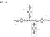
- (a) One approach, as illustrated in
Fig. 1A , while using a simple structure, is enabled to implement a four-body interaction.Fig. 1A is a diagram based on a diagram a ofFigure 4 ofNPL 1.Fig. 1A illustrates a system in which JPO1 to JPO4 with respective resonance angular frequencies ωr, i (i=1,2,3,4) interact via a single Josephson junction (JJ) (JPO1 to JPO4 with different resonance angular frequencies are illustrated with different patterns according toFigure 4 of NPL 1). - SQUID (Superconducting Quantum Interference Device) loop of each JPO is driven by a flux pump whose amplitude and frequency can be adjusted. An angular frequency ωp, k (t)(k = 1 , 2 , 3 , 4) of a pump signal is close to 2 ω r , i, which is twice an angular frequency of a resonator. In a Josephson Parametric Amplifier (JPA), there is a certain threshold for a strength of a pump, wherein when the strength of the pump exceeds the threshold, the JPA begins to oscillate and outputs a signal with a resonance angular frequency ωr , i even with no input signal. This is called a parametric oscillation. In the present specification, since a resonator is directed to one with parametric oscillation, in
Fig. 1A , the JPA inFigure 4 ofNPL 1 is denoted as JPO. - Local four-body coupling is realized through a nonlinear inductance of the Josephson junction JJ disposed at a center (central JJ).
- Each angular frequency of pump signals for JPO1 to JPO4 is selected to meet the following condition:


- In Equation (1.3), Δk(k=1,2,3,4) is a difference (detuning) between a mode angular frequency ωr , k of k-th JPO and a mode angular frequency (resonance angular frequency) ω c, which is defined by a capacitance and inductance of the central Josephson junction JJ.

- φ 0 = (h/2π)(2e) is a magnetic flux quantum (e is an electric elementary charge) and φ c is a standard deviation of a zero-point magnetic flux variation in a JJ mode.
- EJ is a central Josephson energy and takes a value proportional to a critical current Ic of the Josephson junction.
- gk (k=1,2,3,4) is a magnitude of coupling between the k-th JPO and a mode of the Josephson junction of a central coupler.

- where φ k(k=1,2,3,4) is a zero-point magnetic flux variation in a JPO mode, and C is a capacitance value of a coupling capacitor between a coupler and a qubit.
- In NPL1, it is not clear how to strengthen the four-body interaction with respect to a configuration in
Fig. 1A .
(b) The other approach uses a Josephson Ring Modulator (JRM), as illustrated inFig. 1B. Fig. 1B is a diagram based on SupplementaryFigure 8 ofNPL 1. InFig. 1B , JPA in SupplementaryFigure 8 of Supplementary Note 8 ofNPL 1 is denoted as JPO. Microwave drive signals with equal signal strength but opposite phase (as shown with solid and dashed arrows for capacitors Cx and Cy) trigger four-body coupling among the JPOs. A tunable four-body interaction is implemented by using an imbalanced shunted Josephson Ring Modulator (JRM). JRM includes two pairs of Josephson Junctions (JJs). In each pair, the Josephson junctions are connected in series. The two pairs of Josephson junctions are connected in parallel between a first node and a second node, where the first node is a connection node of JPO1 and JPO2, and the second node is a connection node of JPO3 and JPO4. Microwave drive signals are applied to the first and second nodes via the capacitors Cx, respectively, and microwave drive signals each having an opposite phase of the microwave drive signals applied to the capacitors Cx are applied via capacitors Cy to each junction of the two sets of Josephson Junctions (JJs) connected in parallel. - In this case, to implement a four-body interaction, when a combination of oscillation angular frequencies that the JPO1 to JPO4 should meet and an angular frequency ωd of drive signals input from the capacitors Cx and Cy, for example, is given as


where
- The second term on the right side of Equation (1.8) is a four-body interaction term.

- As a configuration of a related technology similar to
Fig. 1A , Patent Literature (PTL) 2, for example, discloses a circuit that uses a lumped element type JPO, as illustrated inFig. 2 . The circuit includes four JPO1 (120A) to JPO4 (120D) and acoupler 121.Coupler connection portions 124A to 124D of the JPO1 (120A) to JPO4 (120D) and thecoupler 121, which includes a Josephson junction (JJ), are capacitively coupled via capacitors (coupling capacitors) 131A to 131D, respectively. Readoutcircuit connection portions 122A to 122D of JPO1 (120A) to JPO4 (120D) are capacitively coupled toreadout circuits 140A to140D viacapacitors 132A to 132D, respectively. JPO1 (120A) to JPO4 (120D) are connected tosignal generation parts 150A to 150D viacontrol lines 123A to 123D, respectively. Thesignal generation parts 150A to 150D generate pump signals to generate magnetic fluxes through SQUID loops of JPO1 (120A) to JPO4 (120D). Anonlinear element 110 of thecoupler 121 is an element that can be regarded as an LC resonator with a Josephson junction (JJ) as a nonlinear inductance. Thenonlinear element 110 may be a SQUID including two Josephson junctions (JJ). -
- [PTL 1] International Publication No.
WO 2017/001404 - [PTL 2] International Publication No.
WO 2021/014885 - [PTL 3]
U.S. Patent No. 10262276 B1 -
- [NPL 1] Puri, et. al., "Quantum annealing with all-to-all connected nonlinear oscillators", Nature Communications 8, 15785 (2017)
- [NPL 2] "Introduction to Quantum Electromagnetic Circuits", International Journal of Circuit Theory and Applications 45, 897 (2016)
- [NPL 3] Z. Wang et al., "Quantum Dynamics of a Few-Photon Parametric Oscillator", Physical Review X 9, 021049 (2019)
- In
NPL 1 andPTL 2, illustrated inFig. 1A andFig. 2 , there is no reference to an approach to strengthen a four-body interaction. The configuration ofFig. 1B allows the strength of the four-body interaction to be adjusted but requires another external input (microwave drive signals input in opposite phases to the capacitors Cx and Cy). - Accordingly, it is an object of the present disclosure to provide a superconducting quantum circuit enabled to strengthen a four-body interaction by a circuit configuration itself, without requiring any other external input.
- According to one of aspects of the present disclosure, there is disclosed a superconducting quantum circuit including first to fourth qubits and a coupler that couples the first to fourth qubits with a four-body interaction,
- wherein the coupler includes: first and second electrodes arranged opposed to each other; and a nonlinear element including a Josephson junction and bridging the first and second electrodes,
- wherein each of the first to fourth qubits includes a resonator including: a loop circuit with a first superconducting line, a first Josephson junction, a second superconducting line and a second Josephson junction connected in a ring-shape; and a capacitor connected in parallel to the loop circuit,
- wherein the first and second qubits are capacitively coupled to the first electrode of the coupler, and the third and fourth qubits are capacitively coupled to the second electrode of the coupler, and
- wherein a magnitude relationship among a capacitance value C of a capacitive coupling between each of the first to fourth qubits and the coupler, a capacitance value CJ of the capacitor connected in parallel to the loop circuit of each of the first to fourth qubits, and a capacitance value Cg between the first and second electrodes of the coupler is set to CJ > Cg > C.
- According to the present disclosure, it is possible to provide a superconducting quantum circuit enabled to strengthen a four-body interaction by the circuit configuration itself, without requiring another external input.
-
- [
Fig. 1A] Fig. 1A is a diagram illustrating a related art. - [
Fig. 1B] Fig. 1B is a diagram illustrating a related art. - [
Fig. 2] Fig. 2 is a diagram illustrating a related art. - [
Fig. 3] Fig. 3 is a diagram schematically illustrating an example embodiment. - [
Fig. 4] Fig. 4 is a diagram schematically illustrating the example embodiment. - [
Fig. 5] Fig. 5 is a diagram schematically illustrating the example embodiment. - [
Fig. 6] Fig. 6 is a diagram illustrating the example embodiment. - [
Fig. 7] Fig. 7 is a diagram schematically illustrating an example. - [
Fig. 8] Fig. 8 is a diagram schematically illustrating a variation example. - [
Fig. 9] Fig. 9 is a diagram schematically illustrating a variation example. - [
Fig. 10] Fig. 10 is a diagram illustrating the example embodiment. - The following describes example embodiments of the present disclosure.
Fig. 3 is a diagram illustrating a circuit configuration of an example embodiment. InFig. 3 , illustration of a readout circuit connected to each JPO illustrated inFig. 2 is omitted. In the present example embodiment, resonant frequencies of each JPO and a coupler are made close to each other to strengthen a four-body interaction. They are made close to each other in a range that satisfies a condition described below. Also, in the present example embodiment, conditions are imposed on capacitance to prevent from strengthening unnecessary interactions other than the four-body interaction. - The example embodiment provides a condition for a parameter setting to strengthen a circuit parameter dependency of the four-body interaction and the four-body interaction.
- Referring to
Fig. 3 , four JPO1 (20A) to JPO4 (20D) and acoupler 21 are provided. JPO1 (20A) to JPO4 (20D) are connected to thecoupler 21 by capacitive coupling throughcoupling capacitors 31A to 31D, respectively. In the following example embodiment, a lump element type is used for each JPO, but it is of course possible to use a distributed element type. - The
coupler 21 includes anonlinear element 10 that includes a Josephson junction (JJ) and acapacitor 15 connected in parallel to thenonlinear element 10. - JPO1 (20A) to JPO4 (20D) include SQUIDs (SQUID loops) 210A to 210D in which first
superconducting portions 203A to 203D,first Josephson junctions 201A to 201D, secondsuperconducting portions 204 A to 204D and second Josephson junctions 202A to 202D are connected in a ring, respectively,magnetic field generators 207A to 207D, and capacitors 206A to 206D, respectively. Themagnetic field generators 207A to 207D generate magnetic flux through theSQUID loops 210A to 210D by pump signals supplied to controllines 23A to 23D from signal generation parts (not shown), respectively. The capacitors 206A to 206D are connected between the firstsuperconducting portions 203A to 203D and the secondsuperconducting portions 204A to 204D, respectively. The secondsuperconducting portions 204A to 204D are connected to ground, the firstsuperconducting portions coupler 21 viacoupling capacitors superconducting portions coupler 21 viacoupling capacitors - CJ is a capacitance value of each of the capacitors 206A to 206D of JPO1 (20A) to JPO4 (20D), Cg is a capacitance value of the
capacitor 15 in thecoupler 21, and C is a capacitance value of each of thecoupling capacitor 31A through 31D. -
Fig. 4 illustrates a schematic example of a configuration (wiring pattern) of JPO1 to JPO4 and thecoupler 21 where JPO1 to JPO4 are made of a lumped element type configuration, as one example ofFig. 3 . Thecoupler 21 includes first andsecond electrodes 16 and 18 (made of superconducting material) that are bridged by thenonlinear element 10. Thefirst electrode 16 includes first and second opposingportions second electrode 18 includes third and fourth opposingportions coupler 21 inFig. 4 , thecapacitor 15, which is shunt-connected (connected in parallel) to the Josephson junction (JJ), corresponds to a capacitance between the first andsecond electrodes Fig. 4 , a ground pattern (ground plane) surrounding the first andsecond electrodes - JPO1 (20A) to JPO4 (20D) are configured as waveguide resonators that are terminated to ground via the
SQUID 210A to 210D, respectively. The waveguide resonator modulates the magnetic flux penetrating through theSQUID loops 210A to 210D by pump signals (microwaves) fromcontrol lines 23A to 23D, at about twice the frequency of the resonance frequency. This causes parametric oscillation. - In JPO1 (20A) and JPO2 (20B), end portions of conductive portions (waveguides made of superconducting material) 205A and 205B (corresponding to
coupler connection parts Fig. 3 ) connecting to the firstsuperconducting portions SQUIDs portions first electrode 16 of thecoupler 21, respectively. Capacitance value C of thecoupling capacitors portions first electrode 16 of thecoupler 21. In JPO3 (20C) and JPO4 (20D), end portions of conductive portions (waveguides made of superconducting material) 205C and 205D (corresponding tocoupler connection parts Fig. 3 ) connecting to the firstsuperconducting portions SQUIDs portions second electrode 18 of thecoupler 21, respectively. Capacitance value C of thecoupling capacitors portions second electrode 18 of thecoupler 21. Capacitors 206A to 206D of JPO1 (20A) to JPO4 (20D) correspond to a capacitance between thefirst superconducting portion 203A to 203D of theSQUID 210A to 210D and ground, respectively. InFig. 4 , ground patterns (ground planes) on both sides of the conductive portions (coplanar waveguides) 205A to 205D of JPO1 (20A) to JPO4 (20D) are omitted. - According to the example embodiment, the following relationship is held.

- By setting a resonance angular frequency ω of each JPO from JPO1 (20A) to JPO4 (20D) and a resonance angular frequency of the
coupler 21 close together, a strength of the four-body interaction (magnitude of coupling constant) is able to be set large. - Derivation of a four-body interaction strength (coupling constant) g(4) for JPO1 (20A) to JPO4 (20D) is outlined below (details will be described later).
- Following a standard approach in this field (e.g., NPL 2), a magnetic flux degree of freedom is set in a circuit. One magnetic flux degree of freedom is set for each JPO and two for the coupler. This is used to write down a Hamiltonian for a classical circuit. The Hamiltonian is quantized using a standard method (see NPL 2). The Hamiltonian quantized Htotal is given as Equation (2.1). In the present specification, the notation of ^H with a hat as a quantized Hamiltonian is not used, as in the case of the
PTL 2.
- In Equation (2.2), HJPO,i is a Hamiltonian of each JPOi (i=1,...,4) and Hcoupler is a Hamiltonian of the
coupler 21. - a; and ai + are creation and annihilation operators of boson corresponding to JPOi (i=1,...,4), respectively (in the present specification, no hat is attached to the creation and annihilation operators either).
- Since the
coupler 21 has two magnetic flux degrees of freedom, thecoupler 21 has two modes for a boson. They are represented by creation and annihilation operators ag + and ag + +, and ag- and ag- + with regard to a boson, respectively. - Htotal includes an interaction of each JPO and the
coupler 21. - g+ and g_ are strength of the interaction between each JPO and the two degrees of freedom of the
coupler 21. These can be expressed in terms of circuit parameters. - s; is given as follows:

- Since each JPO interacts with the
coupler 21, it is conceived that the JPOs also indirectly interacts with each other through interaction with thecoupler 21. By variable transforming into a form that incorporates influence of thecoupler 21 on each JPO, the interaction between each JPO and thecoupler 21 is transformed into the four-body interaction among the JPOs. - That is, the Hamiltonian can be transformed into a Hamiltonian in a form in which the JPOs directly interact. This variable transformation is expressed as a unitary transformation using a unitary matrix U in Equation (2.4).

where ω, ω+, and ω- are resonance angular frequencies of thecoupler 21 corresponding to ai, ag+, and ag-. Difference in angular frequencies between different JPOs is not taken into consideration.

- After performing the unitary transformation, the boson of each JPO is represented in a rotation coordinate system. A frequency of rotation of the coordinate system is different for each JPO. JPOi (i=1,...,4) are represented by coordinate systems that rotate at half a frequency of the pump signals applied to the
magnetic field generators 207A to 207D that generate magnetic fluxes to be applied to the SQUID loops of JPOi. Frequencies of the pump signals are different to each other for JPOi (i=1,...,4). - With transition to the rotational coordinate system, a temporally oscillating terms appear in the Hamiltonian. These oscillating terms are averaged at a time scale of interest and can be neglected because their positive and negative values are cancelled out (rotating wave approximation). Due to a difference in pump signal frequencies, many of terms representing interactions among JPOs and between JPOs and the
coupler 21 oscillate, and these terms are neglected. - However, there are some interaction terms that do not oscillate, and they remain. The transition to a rotational coordinate system and the rotating wave approximation are a standard method used to focus on a behavior in a time scale characteristic to JPO.
- By focusing on the various transformations and the characteristic time scale described above, it is possible to estimate the strength of an interaction between/among JPOs that occurs through the coupler.
- Hamiltonian H'total obtained through the above process is given as follows (2.7).

- In Equation (2.7), H'JPO,i and H'coupler are results of transformations of HJPO,i and Hcoupler, respectively.
- In Equation (2.7), g(4) is a strength of the four-body interaction (coupling constant), which is given by the following Equation (2.8), using parameters of the circuit.

- In Equation (2.8),
- ω and ω- are resonance angular frequencies of the JPOs and the
coupler 21, respectively. - CJ, Cg, and C are capacitance values of capacitors (206A to 206D) of each JPO, the capacitor (15) of the
coupler 21, and coupling capacitors (31A to 31D) between each of JPOs and thecoupler 21, respectively, as described above. - e is the electric elementary charge (approximately 1.6 × 10(-19) coulombs).
- According to the present example embodiment, for example, it is possible to enlarge the coupling constant g(4) of the four-body interaction from the strength of the four-body interaction (coupling constant ) expressed in Equation (2.8) by the following approaches.
- However, g(4) in Equation (2.8) is derived on assumption that as for interaction between each JPO and the
coupler 21, a parameter g' given by the following Equation (2.9) is sufficiently smaller than 1 (g' is a dimensionless quantity quantity).
- In the example embodiment, while keeping a value of g' small, the coupling constant g(4) for the four-body interaction is enlarged.
- More specifically, letting


- In this case, the following holds.

-

- To enlarge the coupling constant g(4) while keeping g' small, the capacitance Cg of the
capacitor 15 of thecoupler 21 and capacitance C of each of thecoupling capacitors 31A to 31D must be made small. - Since one of circuit parameters that characterizes each JPO is the capacitor CJ of each JPO, the capacitance Cg of the
capacitor 15 of thecoupler 21 is set to be smaller than the capacitor CJ of each JPO. Note that Cg is also included in g' of Equation (2.9). - To increase the coupling constant g(4) for the four-body interaction, the capacitance C of each of the
coupling capacitors 31A to 31D must also be reduced. Since this overlaps withCondition 4 below, only the capacitance Cg of thecapacitor 15 of thecoupler 21 is considered in the following. - In order to realize a four-body interaction network which the quantum annealing of the LHZ scheme assumes, it is necessary to weaken two-body interaction in which only two of the four JPOs interact with each other.
- A strength of each two-body interaction between JPO1 and JPO2, and between the JPO3 and JPO4 in
Fig. 3 andFig. 4 is given by the following Equation (2.14).
- A strength of each two-body interaction between JPO1 and JPO3, between JPO1 and JPO4, between JPO2 and JPO3, and between JPO2 and JPO4 is given by the following Equation (2.15).

- In the example embodiment, the following condition is met to weaken these two-body interactions.
- Qualitatively, the four-body interaction is able to be strengthened with the conditions 1-4 met.
Following settings meet the four conditions 1-4 above. - Frequency of JPO ω/(2π): 10 GHz (gigahertz)
- Frequency of the
coupler 21 ω-/(2π): 9.98 GHz - Capacitance of each JPO Cj: 1000 fF (femtofarad)
- Capacitance of the coupler Cg : 200fF
- Coupling capacitance between each JPO and the coupler 21 C: 1fF
- The Josephson junction is adjusted so that the above frequencies are realized.
- With this setting, a strength of the four-body interaction: g(4)/(2π) is given as follows.


- The parameter g' in Equation (2.9) (which is assumed to be sufficiently smaller than 1) is about 0.28.
- The strength of the four-body interaction: g(4)/(2π)


NPL 1.) -
Fig. 5 illustrates changes in coupling constants g(4) and g' when only capacitance Cg of thecoupler 21 is changed. InFig. 5 , g(4)/(2π) and g'/(2π) are illustrated. InFig. 5 , frequency ω-/(2π) of thecoupler 21 is fixed at the above setting (9.98 GHz). - It can be seen that the strength of the four-body interaction (coupling constant) g(4) increases as the capacitance Cg of the
coupler 21 is made smaller. The reason why the four-body interaction is strengthened can be interpreted as follows. - In the superconducting quantum circuit of the above example embodiment, the four-body interaction among JPOs is realized by the following two elements.
- interaction between JPOs and the
coupler 21, and - nonlinearity when the
coupler 21 is quantized. - As capacitor Cg of the
coupler 21 is reduced, the nonlinearity of thecoupler 21 is increased, as a result of which the four-body interaction is strengthened. - Since g' in Equation (2.9) is kept small, the interaction between JPOs and the
coupler 21 is not strengthened, but instead, the four-body interaction is strengthened by making the capacitance Cg of thecoupler 21 smaller. - As described above, in the example embodiment, by adjusting circuit parameters in consideration of the above conditions and substituting the circuit parameters into Equation (2.8) which expresses the coupling constant g(4), it is possible to realize a circuit in which the four-body interaction is strong and other interactions, i.e., the two-body interaction between two of the four JPOs are weakened.
-
Fig. 6 illustrates a non-limiting example of the above example embodiment.Fig. 6 is a schematic diagram of a wiring pattern (planar circuit) of a superconducting quantum circuit fabricated on a substrate such as silicon. -
Fig. 6 illustrates a planar configuration of acoupler 21, in which four qubits (quantum bits) are configured with four JPO1 (20A) to JPO4 (20D) of a lumped element type, and these four qubits (quantum bits) are coupled with the four-body interaction. - JPO1 (20A) to JPO4 (20D) of the lumped element type are configured with a linear (not nonlinear) inductance, a capacitance component, and a resonator with a nonlinear element including a Josephson junction.
- In the example embodiment, the
coupler 21 and JPO1 to JPO4 are realized by lines (wirings) formed by superconductors on a substrate, for example. Silicon (Si) is used as the substrate, but an electronic material such as sapphire or a compound semiconductor material (group IV, group III-V and group II-VI) may be used. The substrate is preferably a single crystal but may be a polycrystalline or amorphous. As a material of the line (wiring material), Nb (niobium) or Al (aluminum) may be used, for example, though not limited thereto. Any metal that becomes superconductive at a cryogenic temperature may be used, such as niobium nitride, indium (In), lead (Pb), tin (Sn), rhenium (Re), palladium (Pd), titanium (Ti), molybdenum (Mo), tantalum (Ta), tantalum nitride, and an alloy containing at least one of the above metals. In order to achieve superconductivity, a coupler circuit is used in a temperature environment of about 10 mK (millikelvin) achieved by a refrigerator. - Referring to
Fig. 6 , a planar shape of afirst electrode 16 is an approximately trapezoidal and is of a shape with rotated about 45 degrees counterclockwise. First and second opposingportions first electrode 16 are extended, respectively, from vicinities of intersections between an upper side and oblique sides (legs) of the trapezoid toward a top and left sides in the drawing, i.e., toward locations where theJPO second electrode 18 is of a shape of an inverted trapezoid where a trapezoid is rotated clockwise by approximately 135 degrees. Third and fourth opposingportions second electrode 18 are extended, respectively, from vicinities of intersections of an upper side and oblique sides (legs) of the trapezoid toward a bottom side and a right side in the drawing, i.e., toward locations where theJPO first electrode 16 and thesecond electrode 18 are arranged with respective bottom sides of the trapezoids facing each other, and a planar shape thereof, when aligned with the opposingportions - The
first electrode 16 has a protrusion 16C which protrudes downward in the drawing in a vicinity of an intersection of one end of a lower base and one of the oblique sides of thefirst electrode 16. Thesecond electrode 18 has a cut portion 18C obtained by cutting off thesecond electrode 18 so as to be in parallel to the protrusion 16C of thefirst electrode 16 in a vicinity of an intersection of one end of the lower base and one of the oblique sides of thesecond electrode 18. Anonlinear element 10, such as a SQUID, is arranged in a gap between the protrusion 16C, which is located in a vicinity of an intersection of one end of the lower base and one of the oblique sides of thefirst electrode 16, and the cut portion 18C, which is located in a vicinity of an intersection of one end of the lower base and one of the oblique sides of thesecond electrode 18. A configuration illustrated inFig. 6 makes a placement area of thecoupler 21 compact with a diagonally arranged configuration of thefirst electrode 16 and thesecond electrode 18 in thecoupler 21. - JPO1 (20A) to JPO4 (20D) include coplanar waveguides (Coplanar Waveguides) 25A, 25B, 25C and 25D and
SQUIDs coplanar waveguides SQUIDs control lines SQUIDs control lines - Connection portions (waveguides for I/O) 22A to 22D for connecting to readout circuits are capacitively coupled via
capacitors 32A to 32D with JPO1 (20A) to JPO4 (20D), respectively. InFig. 6 , the connection portions (coplanar waveguides for I/O) 22A, 22B, 22C, and 22D for connecting to the readout circuits, respectively, are shown in part. Each wiring pattern of the connection portions (coplanar waveguides for I/O) 22A to 22D may have a configuration extended to a chip periphery and, for example, connected to a wiring substrate or the like (not shown) via a bump electrode or the like. Each wiring pattern of the connection portions may be connected to a measurement device or the like outside a refrigerator via a readout line (cable) or the like. InFig. 6 , thecapacitor 15 illustrated inFig. 4 is omitted. - In an example illustrated in
Fig. 6 , the superconducting quantum circuit apparatus includesair bridge wirings control lines air bridge wirings JPO - In
Fig. 6 , a cross section along an A-A line orthogonal to thecontrol line 23D is schematically illustrated in a balloon. A cross section for thecontrol lines 23A to 23C is also configured in an identical manner. For example, a wiring layer is formed on a surface of asubstrate 42 of silicon, on which JPOs 20 (20A to 20D), and the coupler (21) in the center are formed. Thecontrol line 23D is configured as a coplanar waveguide in the same wiring layer. Ground patterns 40-1 and 40-2 are provided on both sides of thecontrol line 23D (wiring) in a longitudinal direction, via gaps, respectively. Theair bridge wiring 27D, which is made of a superconducting material (e.g., Al or the like), is formed in such a manner that strides over thecontrol line 23D in an arch shape and connects theground patterns 40 on both sides of thecontrol line 23D. An air bridge wiring structure with respect to theground pattern 40 eliminates division of theground pattern 40 into both sides 40-1 and 40-2 by the control line 23 (23A through 23D) which is configured as the coplanar waveguide, resulting in a stabilization of a ground potential of theground plane 40 that surrounds JPO1 (20A) to JPO4 (20D). As a non-limiting example, inFig. 8 , the connection portions (coplanar waveguides for I/O) 22A to 22D for connecting to readout circuits are provided withair bridge wirings control lines 23A through 23D. Theair bridge wirings 28A to 28D of the connection portions (coplanar waveguides for I/O) 22A to 22D also have the same cross-section configuration. - Letting CJ be a capacitance value of a capacitor between each of the
coplanar waveguides 25A to 25D of JPO1 (20A) t0 JPO4 (20D) and ground (206A to 206D inFig. 3 ), Cg a capacitance value of thecapacitor 15 between the first andsecond electrodes coupler 21, and C each of a capacitance value of a coupling capacitor (31A inFig. 2 ) between the first opposingportion 17A of thecoupler 21 and thecoupler connection portion 24A of thecoplanar waveguide 25A of JPO1 (20A), a capacitance value of a coupling capacitor (31B inFig. 2 ) between the second opposingportion 17B of thecoupler 21 and thecoupler connection portion 24B of thecoplanar waveguide 25B of JPO2 (20B), a capacitance value of a coupling capacitor (31C inFig. 2 ) between the third opposingportion 19A of thecoupler 21 and thecoupler connection portion 24C of the coplanar waveguide 25C of JPO3 (20C), and a capacitance value of a coupling capacitor (31D inFig. 2 ) between the fourth opposingportion 19B of thecoupler 21 and thecoupler connection portion 24D of thecoplanar waveguide 25D of JPO4 (20D), the following magnitude relation is set.
coupler 21, the coupling strength of the four-body interaction can be set to be larger. - A length (width) of opposing sides of the first and
second electrodes coupler 21 is longer than width ofcoupler connection part 24A to 24D of thewaveguides 25A to 25D of JPO1 (20A) to JPO4 (20D) which face ends of the first and second opposingportions portions coupler 21. A gap (cap) between the opposing sides of the first andsecond electrodes coupler 21 is smaller than a gap between the ends of thecoupler connection parts coupler connection parts parts parts Fig. 6 , which schematically illustrates the wiring pattern, a capacitance C of thecoupling capacitors 31A to 31D between thewaveguides waveguides 25C and 25D of JPO3 (20C) and JPO4 (20D), and the first and second opposingportions portions electrodes capacitor 15 connected in parallel to the nonlinear element 10). In each ofcross-shaped waveguides 25A to 25D (planar waveguides) of JPO1 (20A) to JPO4 (20D), a length of a side opposed to the ground plane (ground pattern) 40 via a gap, is several times longer than that of an opposing side of the first andsecond electrodes Fig. 6 , each capacitance CJ (206A to 206D inFig. 3 ) of JPO1 (20A) to JPO4 (20D) is found to be larger than the capacitance Cg (15 inFig. 3 ) between the first andsecond electrodes coupler 21. - The strength g(4) of the four-body interaction depends on a detuning of resonant frequencies of the coupler (four-body interaction coupler) 21 and of JPOs (20A to 20D). Therefore, it is possible to control a coupling strength of the four-body interaction by adjusting the resonant frequencies of JPOs (20A to 20D) and the
coupler 21. - The first and
second electrodes coupler 21 are coupled each other viacapacitor 15 and further coupled toJPOs coupling capacitors portions portions JPO 20A andJPO 20B, andJPO 20C andJPO 20D, respectively, are protruded from thefirst electrode 16 and thesecond electrode 18 toward theground plane 40, respectively, and able to be coupled withJPO 20A andJPO 20B, andJPO3 20C andJPO 20D at points spaced away from thefirst electrode 16 and from thesecond electrode 18. - By ensuring spacing between portions of the
first electrode 16 andsecond electrode 18 other than thecoupling capacitors 31A-31D and theground pattern 40 with a large gap (almost equivalent in size as the coupler 21) where no superconductor is deposited, for example, on the order of about 100 µm (micrometers) in length, a stray capacitance between each of the first 16 and thesecond electrode 18 and theground pattern 40 is reduced. - The
capacitor 15 between the first andsecond electrodes coupler 21 robust against a disturbance(s) caused by a magnetic field noise, etc. The reduction of the stray capacitance of the first andsecond electrodes coupler 21 capacitively coupled to each JPO is generally weakened due to the stray capacitance of thecoupler 21, since a contribution ratio of the capacitance that contributes to coupling out of a total capacitance, which is a summation of a self-capacitance (Cg) of thecoupler 21 plus the capacitance C of the coupling capacitor and the stray capacitance of thecoupler 21, is reduced. In the example illustrated inFig. 6 , thecoupler 21 is placed separated from an edge of the ground plane (ground pattern) 40 surrounding thecoupler 21 via a gap of the same extent as a size of thecoupler 21, for example, thus reducing the stray capacitance of thecoupler 21. -
Fig. 7 illustrates a coupler (four-body interaction coupler) 21 of another non-limiting example. InFig. 7 , a planer circuit corresponding to thecoupler 21 illustrated inFig. 4 is illustrated while qubits (quantum bits) (JPO) 20A to 20B are not shown. Referring toFig. 7 , thecoupler 21 of the present variation example, includes afirst electrode 16 configured with right-angle bent sides (lateral (horizontal)side 16A and longitudinal (vertical)side 16B), and asecond electrode 18 configured with right-angle bent sides (lateral (horizontal)side 18A and longitudinal (vertical)side 18B). Thelongitudinal sides second electrodes lateral sides first electrode 16 includes n (seven inFig. 7 )extension portions 16D extending at a predetermined interval parallel to thelateral side 16A from thelongitudinal side 16B to thelongitudinal side 18B of thesecond electrode 18 to have a comb-teeth pattern shape. Thesecond electrode 18 also includesn extension portions 18D extending at a predetermined interval parallel to thelateral side 18A from thelongitudinal side 18B to thelongitudinal side 16B of thefirst electrode 16 to have a comb-tooth pattern shape. Theextension portions extension portions lateral side 16A and theextension portion 18D opposed thereto, and a capacitance between thelateral side 18A and theextension portion 16D opposed thereto are the same value Ca, and a capacitance C1 between thelateral sides 
- Assuming that the
extension portions lateral sides extension portions Fig. 7 . In this case, regarding a capacitance C2 between thelateral sides 
- The capacitance C1 between the first and
second electrodes - With the comb-shaped capacitor between the first and
second electrodes electrodes - The
longitudinal side 16B of thefirst electrode 16 includes a first opposingportion 17A corresponding to acoupler connection part 24A of JPO 20A. and thelateral side 16A of thefirst electrode 16 includes a second opposingportion 17B corresponding to acoupler connection part 24B ofJPO 20B. Each of the first and second opposingportions first electrode 16. In spaces of the U-shaped expanded portions of the first and second opposingportions coupler connection parts - The
longitudinal side 18B of thesecond electrode 18 includes a third opposingportion 19A corresponding to acoupler connection part 24C ofJPO 20C, and thelateral side 18B of thesecond electrode 18 includes a fourth opposingportion 19B corresponding to acoupler connection part 24D ofJPO 20D. Each of the third and fourth opposingportions electrode 18. In the U-shaped expanded portions of the third and fourth opposingportions coupler connection parts - A
nonlinear element 10 is configured by a SQUID disposed between an end of thelongitudinal side 16B of thefirst electrode 16 and an end of thelateral side 18A of thesecond electrode 18. The SQUID included in thenonlinear element 10 which bridges the first electrode 16 (an end of thelongitudinal side 16B) and the second electrode 18 (an end of thelateral side 18A). InFig. 7 , the first electrode 16 (an end of thelongitudinal side 16B) and the second electrode 18 (an end of thelateral side 18A), each of which are bridged by the SQUID designated byreference numeral 10, are illustrated withreference numeral 29, enclosed with a dashed circle as the SQUID bridging portion. Thecoupler 21 further includes acontrol line 51 which applies a magnetic flux to the SQUID from within the same plane. By varying a current (i.e., direct current) supplied to thecontrol line 51, a frequency variable coupler is provided. The external magnetic flux given through thecontrol line 51 from the current control part penetrates through the SQUID loop of the four-body interaction coupler 21, thereby varying an effective self-inductance of the SQUID loop. As a result, the resonance frequency is varied. - In the variation example illustrated in
Fig. 7 , a distance between the electrode and the ground (ground pattern 40) is reduced only partially in a vicinity of theSQUID bridging portion 29 of thefirst electrode 16 and thesecond electrode 18. In the vicinity of theSQUID bridging portion 29, thecontrol line 51 is provided to allow an external magnetic flux to be applied from the immediate vicinity of theSQUID bridging portion 29, as a result of which the magnetic flux through inductive coupling from thecontrol line 51 can be efficiently applied. As described, it is preferable that theground pattern 40 is basically spaced apart from the first andsecond electrodes ground pattern 40 has a portion 30 (ground pattern protruding portion) in the vicinity of theSQUID bridging portion 29 that protrudes itself inwardly to be closer to theSQUID bridging portion 29. Thus, the length of theportion 30 is preferably 1/4 or less of a circumference of an inner circumference of theground plane 40 surrounding theelectrodes - In the
coupler 21 of this configuration, letting CJ be a capacitance value of a capacitor (206A to 206D inFig. 3 ) of the of JPO1 (20A) to JPO4 (20D), Cg be a capacitance value of coupling capacitors (31A to 31D inFig. 3 ) between thecoupler connection parts 24A to 24D of JPO1 (20A) to JPO4 (20D) and the opposingportions 
-
Fig. 8 illustrates a coupler (four-body interaction coupler) 21 of yet another non-limiting example. InFig. 8 , a planer circuit corresponding to thecoupler 21 illustrated inFig. 4 is illustrated while qubits (quantum bits) (JPO) 20A to 20B are not shown. Referring toFig. 8 , thecoupler 21 has a structure such that thegrand pattern 40, which penetrates between first second opposingportions portions coupler connection parts coupler connection parts JPO capacitors 31A-2, 31B-2, 31C-2, and 31D-2, respectively, and the first and second opposingportions portions coupler connection parts capacitor 31A-1, 31B-1, 31C-1, and 31D-1, respectively. The space between thecoupler connection parts JPO portions coupler connection parts JPO portions coupler connection parts JPOs portions coupler connection parts JPOs portions coupling capacitors 31A to 31D with smaller capacitance value than a configuration without ground pattern between coupler connection parts of JPOs and opposing portions (Fig. 7 ). - In the
coupler 21 of this configuration, regarding CJ which is a capacitance value of the capacitor (206A to 206D inFig. 3 ) of the of JPO1 (20A) to JPO4 (20D), Cg which is a capacitance value of the capacitor of thecoupler 21, C which is a capacitance value of coupling capacitors (31A to 31D inFig. 3 ) between thecoupler connection parts 24A to 24D of JPO1 (20A) to JPO4 (20D) and the opposingportions coupler 21, the following magnitude relation holds.
-
Fig. 10 illustrates a schematic diagram of aquantum computer 200 withJPO 20 integrated as a configuration example of another example embodiment. In the configuration illustrated inFig. 10 , each four-body interaction coupler 21 is connected to the fourJPOs 20, respectively, as illustrated inFig. 4 and/orFig. 6 . EachJPO 20 is connected to one through four four-body interaction couplers 21, andJPO 20 is arranged to be shared by a plurality of unit structures to provide a configuration in which a plurality of unit structures illustrated inFig. 3 ,Fig. 4 , andFig. 6 , etc., are arranged. In thequantum computer 200, at least oneJPO 20 is connected to a plurality of four-body interaction couplers 21. Specially, in the example as illustrated inFig. 10 , at least oneJPO 20 is connected to four four-body interaction couplers 21. Thequantum computer 200 may also be described as follows. Thequantum computer 200 includes a plurality of JPOs 20, each of which is connected to one through four four-body interaction couplers 21. The number of the four-body interaction couplers 21 to which eachJPO 20 connects corresponds to how many unit structures share JPOs 20. Thus, in the example illustrated inFig. 10 , thequantum computer 200 includes a plurality of unit structures, and a plurality of unit structures shareJPO 20. In the example illustrated inFig. 10 , 13 superconductingnonlinear JPOs 20 are integrated, but any number of JPOs 20 may be integrated in a similar manner. A current control part and a readout part are not illustrated inFig. 10 , for ease of understanding of the drawing, but as explained with reference toFig. 2 , etc., the current control part and the readout part are used to control and read outJPO 20. - The following describes the derivation of the above equation. As described in
NPL 2,Fig. 9 is a diagram corresponding toFig. 3 . InFig. 9 , Josephson junction is indicated by an x surrounded by a square, and φ1 to φ4 inSQUID loops 210A to 210D of JPO1 to JPO4 represent a magnetic flux penetrating through each SQUID loop. The EJs attached to the two Josephson junctions inSQUID loops 210A to 210D of JPO1 to JPO4 represent the Josephson energy. - As illustrated in
Fig. 9 , magnetic flux φ1 to φ4, φg1 and φg2 are arranged on eachnode 1 to 4, g1 and g2. - In a circuit with an inductor (Josephson junction can be regarded as a nonlinear inductor) and a capacitor (non-dissipative circuit), V = - d φ/dt with respect to a time derivative of the magnetic flux cp (Faraday's law). Therefore, an energy E = (1/2)CV2 of a capacitance branch (voltage V at both ends) is expressed as follows.

- That is, a capacitor energy can be treated as kinetic energy. Let φ be a vector (6-dimensional vector) whose elements are φ 1 to φ 4, φg1, and φ g2.

- In
Fig. 9 , the energy (kinetic energy) of a capacitor branch is given by (3.3).
- Here, Cmat is, as shown in the following Equation (3.4), a circuit matrix (6-rowa and 6 columns matrix) of capacitance branches in
Fig. 9 .
- An element CJ+C of k-th row and k-th column (k=1 to 4) of matrix Cmat is a combined capacitance of two capacitors C and CJ that are connected in parallel to a node k (k=1-4). An element CJ+2C in k-th row and k-th column (k=5, 6) of the matrix Cmat is a combined capacitance of three capacitors C, C and CJ connected in parallel to a node k (k=5, 6). An element of i-th row and j-column (i ≠j, i,j=1-6) of the matrix Cmat is a capacitance between nodes i and j (signs indicate a direction of the capacitor branch).
- A Lagrangian for a circuit in
Fig. 9 is given by Equation (3.5).
- In Equation (3.5), V(φ) is potential energy and is given by Equation (3.6).

where,

-
- EJ is Josephson energy in JPO1-JPO4.
- EJg is Josephson energy in a
coupler 21. - Φi is a magnetic flux penetrating through the SQUID loop of JPO; (i=1,...,4).
- φ g1- φ g2 is a magnetic flux penetrating through the coupler 21 (a difference between respective magnetic fluxes of nodes g1 and g2).
- The kinetic energy of the
Lagrangian 

q1, q2, q3, q4, qg1, and qg2 are a charge of each node. t is a transpose operator.
From Equation (3.10), assuming that the matrix Cmat is normal, we obtain the following.
- Therefore, the kinetic energy in Equation (3.9) can be expressed using vector q as follows.

- In Equation (3.12), I is a unit matrix of 6 × 6. The last Expression in Equation (3.12) uses the fact that the matrix Cmat is a symmetric matrix (component cij(i,j=1,...,6) is cij=cji with respect to subscripts i and j), which is symmetric with respect to a main diagonal, and an inverse matrix Cmat -1 of Cmat is also a symmetric matrix. That is, CmatCmat -1=I. By taking the transpose of both sides of this Equation, we have (Cmat -1)tCmat t=I. Since Cmat is a symmetric matrix, by multiplying both sides by the inverse matrix Cmat -1 from a right side, (Cmat -1)t = Cmat -1, and thus Equation (3.12) holds.
- Expressing potential energy as a function of vector φ (nonlinear function), the Hamiltonian is given as follows.

- Obtaining the inverse matrix Cmat -1 of the matrix Cmat of 6 rows and 6 columns concretely, the Hamiltonian H is given as the following Equation (3.14).

where,


- In Equation (3.14), the Expression at the bottom line, the following is assumed.

- When O(C') is neglected, a product between degrees of freedom of JPO does not appear. Details of calculations are given in section A.1 of the appendix below.
- By converting variables φ and q in the classical Hamiltonian to operators as follows, the Hamiltonian is replaced by a function of the operator (quantization of the Hamiltonian).


where k=1,2,3,4,g1,g2, and a+ k and ak are creation and annihilation operators of boson. e is elementary electric charge (quantum of electricity). In this case, the following commutation relation (4.4) holds.


- In Equations (4.5) and (4.6),


- Since Z1 and Z2 are equal,

- We have




- In Equations (4.11) and (4.13),

- In Equations (4.12) and (4.14),

- Following holds as a commutator (commutation relation) of an operator.


- Therefore, by quantizing the Hamiltonian of a classical system as above, the following is derived. A quantized Hamiltonian is written HQ instead of using a hat.

- Here, O(C') is neglected and higher order terms in an expansion of cos(φ i/φ 0) are neglected.
- Next, let Φi be time-varying so that it can be approximated as follows (reference may be made to NPL 3).


- where,


- In Equation (4.21), a constant term(s) are excluded.
- In addition, δEJ is treated as small and, therefore, δEJ φ 4 Z is neglected.
- Furthermore, at the rightmost side of Equation (4.23), quantities as large as C' (= C/CJ) is neglected.
- Next, a unitary transformation using a unitary matrix Ug of Equation (4.27) is applied on the Hamiltonian of Equation (4.21).

- In Equation (4.27),


s; is given by Equation (3.18). - This unitary transformation is a transformation that incorporates an interaction (

JPOs 1 to 4 and thecoupler 21 in the HQ into the creation/annihilation operator a+ i/ai, etc. - In other words, it is a transformation that perturbatively incorporates an influence of the
coupler 21 on JPO1 to JPO4. - After this unitary transformation, the creation/annihilation operator a+ i/ai is transferred to the rotational coordinate system with oscillation frequency ω p,i/2. (<Note 1>: Since this is after the above unitary transformation, this a; is the degree of freedom of each JPO perturbatively incorporating influence of the coupler 21).


- Then, assuming that ω p,k is sufficiently large for a time scale of interest, a rotating wave approximation that neglects the oscillating term is performed.
At this time,
- O(g'+2), etc., are neglected as small quantity. However, it is assumed that g'_4/Cg is not negligible as compared to other terms (e.g., Δ i below).
- We have the following Hamiltonian H'Q. Details of calculations are given in section A.2.

- In Equation (4.34),


g'+, g'-, and g(4) are expressed using circuit parameters and resonance angular frequencies ω and ω- as follows.


- Note that, since in a result of
NPL 1 corresponding to Equation (4.44), g(4) diverges infinity at capacitance C→0, it is physically wrong. According toNPL 1, the strength of the four-body interaction is proportional to g1g2g3g4 (Equation (1.3) above), each gk (k = 1 to 4) is expressed as (1/C) with respect to a coupling capacitor C between a coupler and a qubit (Equation (1.5) above), and strength of the four-body interaction in Equation (1.3) above diverges to infinity when coupling capacitor C→0. - In the circuit illustrated in
Fig. 9 , each JPO interacts with other JPOs through thecoupler 21. To represent this as a direct interaction between JPOs, in the example embodiment, influence of thecoupler 21 is perturbatively incorporated into JPOs. The JPO, which incorporates the influence of thecoupler 21, realizes the four-body interaction. The following conditions are assigned in a calculation process. -
- (1)

- (2) g'+ and g'_ given by equations (4.43) and (4.44), respectively, satisfy the following relationship.

Note 2 below) - (3) angular frequencies ωp,k (k=1,2,3,4) of pump signals respectively differ greatly, and the rotating wave approximation is valid.
- These conditions have physically following meaning.
- Condition (1) weakens direct interactions between/among JPOs performed without via the
coupler 21. - Condition (2) causes the
coupler 21 not to have a too strong influence and the JPO to have a behavior not deviating from that of the original JPO. - Condition (3) weakens an interaction (two-body interaction between JPOs and an interaction between the JPO and the coupler 21) other than the four-body interaction among JPOs into which the influence of
coupler 21 is incorporated. - When the above conditions are met, the effective Hamiltonian of the circuit is given by Equation (4.34) and the coupling coefficient g(4) of the four-body interaction among JPOs is given by Equation (4.44).
- <Note 2> Note that, when


holds. Thus,
- In the following, details of the above derivation process are explained supplementally.
- Cmat -1 in Equation (3.4) is an inverse matrix of the matrix Cmat, and a value Cij -1 of element (i,j) of the inverse matrix is as follows. Since Cmat -1 is a symmetric matrix, only an upper triangular part of the matrix (including diagonal components) Cij -1(j>=i) is shown.


- Accordingly, the Hamiltonian (classical Hamiltonian) is given by following.


- and assume C' « 1.


The Hamiltonian H is derived as the following Equation (A.20).
- Next, the following examines how each operator is transformed by a matrix Ug [Equation (4.27)] of the unitary transformation.

- Here, s; is as in Equation (3.18).
- Let

fi(1) may be calculated. Therefore, a Taylor expansion of fi(λ) is performed around λ = 0 and set λ = 1.

- For these calculations, the following relations (A.25) to (A.28) are used.




- With these relationships, the following equations (A.29) to (A.34) are obtained. Here, O(g'+ 3) and other factors are neglected.


- Transformation U ω p/2 [Equation (4.31)] to a rotational coordinate system is also performed.
- Then, by the two transformations, for example, a+ iai is transformed as follows.

where an oscillating term(s), which is a term(s) oscillating at each oscillation frequency ω p,i, such as exp(iω p,it), is/are neglected under the rotating wave approximation. - In the following, transformation of each of the other terms in the quantized Hamiltonian HQ [Equation (4.21)] is shown. Here, in HQ, as for terms, where ω, ω +, and ω - are coefficient (such as a+ g+ag+) thereof, up to terms, where g'+ 2 and g'- 2 are coefficient thereof, are shown concretely after the transformation. In the transformation of (ag_+a+g_)4, terms up to a term where g'4 is a coefficient thereof, is shown concretely. For other terms before transformation, O(g'+ 2), etc., after transformation is not shown. The transformation is as follows.

where


where


- Next, using Equations (A.35), (A.39), (A.40), (A.41), and (A.43), the unitary transformation of the following sum included in the HQ [Equation (4.21)] is examined.


- The quantized Hamiltonian HQ [Equation (4.21)] is obtained from Equations (A.34), (A.36), (A.42), (A.47), and (A.52).

- In deriving Equation (A.53), the following equations (A.54) to (A.62) are used.





where
- Note that ag+ and a+ g+ are not products of ai and a+ i, so there is no need to pay attention to them. Equation (4.34) is obtained by eliminating terms ag+ and a+ g+.
- A general flow of the derivation of the four-body interaction among JPOs described above can be said to be similar to the study by Puri et al [NPL 1]. However, the details of the derivation process are quite different, as are the final results. It can be said that the result obtained with the present specification is physically more natural. The circuit analyzed by Puri et al [NPL 1] is essentially the same as in
Fig. 9 . However, inNPL 1, capacitance CJ or Cg is not explicitly indicated. Also, in a derivation process, inNPL 1, the Hamiltonian of the classical circuit is not shown. Further, in the quantum system,NPL 1 does not take into account those corresponding to ag+ and a+ g+ in the present specification. Therefore, inNPL 1, a unitary matrix for the transformation to incorporate the interaction between JPOs and a coupler into JPOs is different from the above Equation (4.27) of the present specification. - In an analysis of Puri et al. (NPL 1), there is no correspondence to g'+ in the above Equation (4.42) of the present specification.
- In the analysis of Puri et al. (NPL 1), g(4) is to diverge to infinity in a limit where JPOs and a coupler become independent (capacitance C → 0 between each JPO and the coupler), which is physically wrong. C → 0 is to be a limit where the approximation improves, and it is strange that the analysis breaks down here.
- g(4) in the above Equation (4.44) becomes g(4) → 0 at capacitance C → 0. Therefore, it can be said that there is a leap in the derivation process of Puri et al.
- The disclosure of each of
PTLs 1 to 3 andNPLs 1 to 3 is incorporated herein by reference thereto. Variations and adjustments of the examples are possible within the scope of the overall disclosure (including the claims) based on the basic technical concept. Various combinations and selections of examples and disclosed elements (including the elements in each of the claims, examples, drawings, etc.) are possible within the scope of the claims of the present application. That is, the present disclosure includes various variations and modifications that could be made by those skilled in the art according to the overall disclosure including the claims and the technical concept. -
- 10, 110: nonlinear element
- 15: capacitor
- 16: electrode (first electrode)
- 16A, 18A: lateral side
- 16B, 18B: longitudinal side
- 16C: protrusion
- 16D, 18D: extension portion
- 17A, 17B: first and second opposing portion
- 18: electrode (second electrode)
- 18C: cut portion
- 19A, 19B: third and fourth opposing portion
- 20A to 20D, 120A to 120D: superconducting qubit (quantum bit) (JPO)
- 21, 121: coupler
- 22A to 22D, 122A to 122D: readout circuit connection portion
- 23A to 23D, 123A to 123D: control line (flux line)
- 24A to 24D, 124A to 124D: coupler connection part
- 25A to 25D: coplanar waveguide
- 26A to 26D: nonlinear element (SQUID)
- 27A to 27D: air bridge wiring
- 28A to 28D: air bridge wiring
- 29: SQUID bridging portion
- 30: portion (ground pattern protruding portion)
- 31A to 31D: capacitor (coupling capacitor)
- 32A to 32D: capacitor
- 40, 40-1, 40-2: ground (GND) pattern (ground plane)
- 41: surface of substrate
- 42: substrate (silicon substrate)
- 43A to 43D, 44A, 44B: gap (gap width)
- 51: control line
- 140A to 140D: readout circuit
- 150A to 150D: signal generation part
- 200: quantum computer
- 201A, 201B, 201C, 201D: first Josephson junction
- 202A, 202B, 202C, 202D: second Josephson junction
- 203A, 203B, 203C, 203D: first superconducting portion
- 204A, 204B, 204C, 204D: second superconducting portion
- 205A, 205B, 205C, 205D: conductive portion
- 206A, 206B, 206C, 206D: capacitor
- 207A, 207B, 207C, 207D: magnetic field generator
- 210A, 210B, 210C, 210D: SQUID (SQUID loop)
Claims (9)
- A superconducting quantum circuit comprising:first to fourth qubits; anda coupler that couples the first to fourth qubits with a four-body interaction,wherein the coupler includes:first and second electrodes arranged opposed to each other; anda nonlinear element including a Josephson junction and bridging the first and second electrodes,wherein each of the first to fourth qubits includes a resonator including:a loop circuit with a first superconducting line, a first Josephson junction, a second superconducting line and a second Josephson junction connected in a ring-shape; anda capacitor connected in parallel to the loop circuit,wherein the first and second qubits are capacitively coupled to the first electrode of the coupler, andthe third and fourth qubits are capacitively coupled to the second electrode of the coupler, andwherein a magnitude relationship among a capacitance value C of a capacitive coupling between each of the first to fourth qubits and the coupler, a capacitance value CJ of the capacitor connected in parallel to the loop circuit of each of the first to fourth qubits, and a capacitance value Cg between the first and second electrodes of the coupler is set to Cj > Cg > C.
- The superconducting quantum circuit according to claim 1, wherein a strength of the four-body interaction is expressed with a numerator that includes a fourth power of C and a denominator that includes a product of a square of CJ multiplied by a cube of a sum of Cg and C, and a difference between a resonance angular frequency of the coupler and a resonance angular frequency of each qubit,
by making Cg smaller as compared to CJ, the strength of the four-body interaction being set larger. - The superconducting quantum circuit according to claim 1 or 2, wherein by making C smaller than CJ, a two-body interaction between two qubits is weakened.
- The superconducting quantum circuit according to claim 1 or 2, wherein as for a ratio
ω/ω-= 1 ± δ,where ω is a resonance angular frequency of each of the qubits and ω- is a resonance angular frequency of the coupler,ω is brought closer to ω - within a range satisfying
- The superconducting quantum circuit according to any one of claims 1 to 4, wherein each of the first to fourth qubits has the resonator terminated with the loop circuit and includes a magnetic flux generator to which a pump signal is fed, the magnetic flux generator generating a magnetic flux that intersects the loop circuit and causing the resonator to perform a parametric oscillation.
- The superconducting quantum circuit according to any one of claims 1 to 4, wherein in each of the first to fourth qubits,the second superconducting line of the loop circuit is connected to ground,the first superconducting line side of the loop circuit is connected to a waveguide, andthe capacitor connected in parallel to the loop circuit includes a stray capacitance between the waveguide and ground, whereinthe waveguide of each of the first and second qubits has an end thereof capacitively coupled to the first electrode of the coupler, andthe waveguide of each of the third and fourth qubits has an end thereof capacitively coupled to the second electrode of the coupler.
- The superconducting quantum circuit according to any one of claims 1 to 4, wherein in the coupler, the nonlinear element includes a loop circuit, in which, a first superconducting line, a first Josephson junction, a second superconducting line and a second Josephson junction are connected in a ring-shape.
- The superconducting quantum circuit according to any one of claims 1 to 7, wherein the first to fourth qubits configured as Josephson parametric oscillators and the coupler constitute a unit structure in a quantum computer.
- The superconducting quantum circuit according to claim 8, comprising a plurality of the unit structures, wherein a quantum computer is configured to have at least one qubit among the first to fourth qubits constituting the unit structure shared by one or a plurality of other unit structures.
Applications Claiming Priority (1)
| Application Number | Priority Date | Filing Date | Title |
|---|---|---|---|
| PCT/JP2022/015706 WO2023188041A1 (en) | 2022-03-29 | 2022-03-29 | Superconducting quantum circuit |
Publications (3)
| Publication Number | Publication Date |
|---|---|
| EP4503903A1 true EP4503903A1 (en) | 2025-02-05 |
| EP4503903A4 EP4503903A4 (en) | 2025-05-21 |
| EP4503903B1 EP4503903B1 (en) | 2026-03-18 |
Family
ID=88200162
Family Applications (1)
| Application Number | Title | Priority Date | Filing Date |
|---|---|---|---|
| EP22935189.5A Active EP4503903B1 (en) | 2022-03-29 | 2022-03-29 | Superconducting quantum circuit |
Country Status (4)
| Country | Link |
|---|---|
| US (1) | US20250301922A1 (en) |
| EP (1) | EP4503903B1 (en) |
| JP (1) | JP7786560B2 (en) |
| WO (1) | WO2023188041A1 (en) |
Family Cites Families (4)
| Publication number | Priority date | Publication date | Assignee | Title |
|---|---|---|---|---|
| EP3113084B1 (en) | 2015-06-29 | 2020-12-09 | Parity Quantum Computing GmbH | Quantum processing device and method |
| CA2968830C (en) * | 2017-05-29 | 2024-04-02 | Socpra Sciences Et Genie S.E.C. | Quantum processor, and method of quantum processing |
| JP7279792B2 (en) * | 2019-07-19 | 2023-05-23 | 日本電気株式会社 | Resonators, Oscillators, and Quantum Computers |
| US12021520B2 (en) * | 2019-07-19 | 2024-06-25 | Nec Corporation | Resonator, oscillator, and quantum computer |
-
2022
- 2022-03-29 US US18/851,131 patent/US20250301922A1/en active Pending
- 2022-03-29 EP EP22935189.5A patent/EP4503903B1/en active Active
- 2022-03-29 JP JP2024510832A patent/JP7786560B2/en active Active
- 2022-03-29 WO PCT/JP2022/015706 patent/WO2023188041A1/en not_active Ceased
Also Published As
| Publication number | Publication date |
|---|---|
| JP7786560B2 (en) | 2025-12-16 |
| US20250301922A1 (en) | 2025-09-25 |
| WO2023188041A1 (en) | 2023-10-05 |
| EP4503903A4 (en) | 2025-05-21 |
| EP4503903B1 (en) | 2026-03-18 |
| JPWO2023188041A1 (en) | 2023-10-05 |
Similar Documents
| Publication | Publication Date | Title |
|---|---|---|
| Burkard et al. | Superconductor–semiconductor hybrid-circuit quantum electrodynamics | |
| Cottet et al. | Cavity QED with hybrid nanocircuits: from atomic-like physics to condensed matter phenomena | |
| US9059674B2 (en) | Multi-tunable superconducting circuits | |
| Bell et al. | Quantum superinductor with tunable nonlinearity | |
| Sakai et al. | Excitation spectra of the two impurity Anderson model. I. Critical transition in the two magnetic impurity problem and the roles of the parity splitting | |
| CN112331693A (en) | An easily scalable, high-fidelity superconducting quantum chip structure and operation method | |
| US12188999B2 (en) | Superconducting quantum circuit | |
| US20220261676A1 (en) | Resonator, oscillator, and quantum computer | |
| EP4125131B1 (en) | Coupler and calculating device | |
| Garcia et al. | On the application of finite methods in time domain to anisotropic dielectric waveguides | |
| US20180017603A1 (en) | Oscillation device, computing device, and measurement method | |
| EP4503903B1 (en) | Superconducting quantum circuit | |
| US10984976B1 (en) | Microfabricated ion trap chip with an integrated microwave antenna | |
| EP4546999A1 (en) | Superconducting quantum circuit | |
| US20230318601A1 (en) | Superconducting quantum circuit apparatus | |
| US20250272590A1 (en) | Superconducting quantum circuit apparatus | |
| Jacobs et al. | Fluctuation-induced phase in in a transverse magnetic field: Theory | |
| Block et al. | Nucleation of optically excited solitons and breathers in trans-polyacetylene | |
| US20220181534A1 (en) | Superconducting metamaterials for quantum simulations and qubit addressability in quantum processors | |
| Hatano et al. | Gate-voltage dependence of inter dot coupling and Aharanov–Bohm oscillation in laterally coupled vertical double dot | |
| Scigliuzzo | Effects of the environment on quantum systems: decoherence, bound states and high impedance in superconducting circuits | |
| Gunnarsson et al. | Vibronic spectroscopy of an artificial molecule | |
| Enderle et al. | Excitations of the Field-Induced Quantum Soliton Lattice in CuGeO 3 | |
| de Castilho et al. | Modulated phases in a spin model with Dzyaloshinskii-Moriya interactions | |
| EP4552046B1 (en) | Charged particle trap operation |
Legal Events
| Date | Code | Title | Description |
|---|---|---|---|
| STAA | Information on the status of an ep patent application or granted ep patent |
Free format text: STATUS: THE INTERNATIONAL PUBLICATION HAS BEEN MADE |
|
| PUAI | Public reference made under article 153(3) epc to a published international application that has entered the european phase |
Free format text: ORIGINAL CODE: 0009012 |
|
| STAA | Information on the status of an ep patent application or granted ep patent |
Free format text: STATUS: REQUEST FOR EXAMINATION WAS MADE |
|
| 17P | Request for examination filed |
Effective date: 20241025 |
|
| AK | Designated contracting states |
Kind code of ref document: A1 Designated state(s): AL AT BE BG CH CY CZ DE DK EE ES FI FR GB GR HR HU IE IS IT LI LT LU LV MC MK MT NL NO PL PT RO RS SE SI SK SM TR |
|
| REG | Reference to a national code |
Ref country code: DE Ref legal event code: R079 Free format text: PREVIOUS MAIN CLASS: H10N0060100000 Ipc: G06N0010400000 Ref country code: DE Ref legal event code: R079 Ref document number: 602022032783 Country of ref document: DE Free format text: PREVIOUS MAIN CLASS: H10N0060100000 Ipc: G06N0010400000 |
|
| A4 | Supplementary search report drawn up and despatched |
Effective date: 20250422 |
|
| RIC1 | Information provided on ipc code assigned before grant |
Ipc: H03K 17/92 20060101ALN20250414BHEP Ipc: H10N 60/12 20230101ALN20250414BHEP Ipc: G06N 10/40 20220101AFI20250414BHEP |
|
| DAV | Request for validation of the european patent (deleted) | ||
| DAX | Request for extension of the european patent (deleted) | ||
| GRAP | Despatch of communication of intention to grant a patent |
Free format text: ORIGINAL CODE: EPIDOSNIGR1 |
|
| STAA | Information on the status of an ep patent application or granted ep patent |
Free format text: STATUS: GRANT OF PATENT IS INTENDED |
|
| RIC1 | Information provided on ipc code assigned before grant |
Ipc: G06N 10/40 20220101AFI20251001BHEP Ipc: H10N 60/12 20230101ALN20251001BHEP Ipc: H03K 17/92 20060101ALN20251001BHEP |
|
| INTG | Intention to grant announced |
Effective date: 20251016 |
|
| GRAS | Grant fee paid |
Free format text: ORIGINAL CODE: EPIDOSNIGR3 |
|
| GRAA | (expected) grant |
Free format text: ORIGINAL CODE: 0009210 |
|
| STAA | Information on the status of an ep patent application or granted ep patent |
Free format text: STATUS: THE PATENT HAS BEEN GRANTED |
|
| AK | Designated contracting states |
Kind code of ref document: B1 Designated state(s): AL AT BE BG CH CY CZ DE DK EE ES FI FR GB GR HR HU IE IS IT LI LT LU LV MC MK MT NL NO PL PT RO RS SE SI SK SM TR |
|
| REG | Reference to a national code |
Ref country code: CH Ref legal event code: F10 Free format text: ST27 STATUS EVENT CODE: U-0-0-F10-F00 (AS PROVIDED BY THE NATIONAL OFFICE) Effective date: 20260318 Ref country code: GB Ref legal event code: FG4D |
|
| REG | Reference to a national code |
Ref country code: IE Ref legal event code: FG4D |
|
| REG | Reference to a national code |
Ref country code: DE Ref legal event code: R096 Ref document number: 602022032783 Country of ref document: DE |
|
| PGFP | Annual fee paid to national office [announced via postgrant information from national office to epo] |
Ref country code: DE Payment date: 20260319 Year of fee payment: 5 |
|
| PGFP | Annual fee paid to national office [announced via postgrant information from national office to epo] |
Ref country code: AT Payment date: 20260414 Year of fee payment: 5 |