EP4503641A1 - Imaging element and imaging device - Google Patents
Imaging element and imaging device Download PDFInfo
- Publication number
- EP4503641A1 EP4503641A1 EP23774334.9A EP23774334A EP4503641A1 EP 4503641 A1 EP4503641 A1 EP 4503641A1 EP 23774334 A EP23774334 A EP 23774334A EP 4503641 A1 EP4503641 A1 EP 4503641A1
- Authority
- EP
- European Patent Office
- Prior art keywords
- pixel group
- light
- green
- blue
- red
- Prior art date
- Legal status (The legal status is an assumption and is not a legal conclusion. Google has not performed a legal analysis and makes no representation as to the accuracy of the status listed.)
- Pending
Links
Images









Classifications
-
- H—ELECTRICITY
- H04—ELECTRIC COMMUNICATION TECHNIQUE
- H04N—PICTORIAL COMMUNICATION, e.g. TELEVISION
- H04N23/00—Cameras or camera modules comprising electronic image sensors; Control thereof
- H04N23/50—Constructional details
- H04N23/55—Optical parts specially adapted for electronic image sensors; Mounting thereof
-
- H—ELECTRICITY
- H04—ELECTRIC COMMUNICATION TECHNIQUE
- H04N—PICTORIAL COMMUNICATION, e.g. TELEVISION
- H04N25/00—Circuitry of solid-state image sensors [SSIS]; Control thereof
- H04N25/10—Circuitry of solid-state image sensors [SSIS]; Control thereof for transforming different wavelengths into image signals
- H04N25/11—Arrangement of colour filter arrays [CFA]; Filter mosaics
- H04N25/13—Arrangement of colour filter arrays [CFA]; Filter mosaics characterised by the spectral characteristics of the filter elements
- H04N25/134—Arrangement of colour filter arrays [CFA]; Filter mosaics characterised by the spectral characteristics of the filter elements based on three different wavelength filter elements
-
- H—ELECTRICITY
- H04—ELECTRIC COMMUNICATION TECHNIQUE
- H04N—PICTORIAL COMMUNICATION, e.g. TELEVISION
- H04N25/00—Circuitry of solid-state image sensors [SSIS]; Control thereof
- H04N25/10—Circuitry of solid-state image sensors [SSIS]; Control thereof for transforming different wavelengths into image signals
- H04N25/11—Arrangement of colour filter arrays [CFA]; Filter mosaics
- H04N25/13—Arrangement of colour filter arrays [CFA]; Filter mosaics characterised by the spectral characteristics of the filter elements
-
- H—ELECTRICITY
- H10—SEMICONDUCTOR DEVICES; ELECTRIC SOLID-STATE DEVICES NOT OTHERWISE PROVIDED FOR
- H10F—INORGANIC SEMICONDUCTOR DEVICES SENSITIVE TO INFRARED RADIATION, LIGHT, ELECTROMAGNETIC RADIATION OF SHORTER WAVELENGTH OR CORPUSCULAR RADIATION
- H10F39/00—Integrated devices, or assemblies of multiple devices, comprising at least one element covered by group H10F30/00, e.g. radiation detectors comprising photodiode arrays
- H10F39/80—Constructional details of image sensors
- H10F39/802—Geometry or disposition of elements in pixels, e.g. address-lines or gate electrodes
- H10F39/8023—Disposition of the elements in pixels, e.g. smaller elements in the centre of the imager compared to larger elements at the periphery
-
- H—ELECTRICITY
- H10—SEMICONDUCTOR DEVICES; ELECTRIC SOLID-STATE DEVICES NOT OTHERWISE PROVIDED FOR
- H10F—INORGANIC SEMICONDUCTOR DEVICES SENSITIVE TO INFRARED RADIATION, LIGHT, ELECTROMAGNETIC RADIATION OF SHORTER WAVELENGTH OR CORPUSCULAR RADIATION
- H10F39/00—Integrated devices, or assemblies of multiple devices, comprising at least one element covered by group H10F30/00, e.g. radiation detectors comprising photodiode arrays
- H10F39/80—Constructional details of image sensors
- H10F39/805—Coatings
- H10F39/8053—Colour filters
-
- H—ELECTRICITY
- H10—SEMICONDUCTOR DEVICES; ELECTRIC SOLID-STATE DEVICES NOT OTHERWISE PROVIDED FOR
- H10F—INORGANIC SEMICONDUCTOR DEVICES SENSITIVE TO INFRARED RADIATION, LIGHT, ELECTROMAGNETIC RADIATION OF SHORTER WAVELENGTH OR CORPUSCULAR RADIATION
- H10F39/00—Integrated devices, or assemblies of multiple devices, comprising at least one element covered by group H10F30/00, e.g. radiation detectors comprising photodiode arrays
- H10F39/80—Constructional details of image sensors
- H10F39/805—Coatings
- H10F39/8057—Optical shielding
-
- H—ELECTRICITY
- H10—SEMICONDUCTOR DEVICES; ELECTRIC SOLID-STATE DEVICES NOT OTHERWISE PROVIDED FOR
- H10F—INORGANIC SEMICONDUCTOR DEVICES SENSITIVE TO INFRARED RADIATION, LIGHT, ELECTROMAGNETIC RADIATION OF SHORTER WAVELENGTH OR CORPUSCULAR RADIATION
- H10F39/00—Integrated devices, or assemblies of multiple devices, comprising at least one element covered by group H10F30/00, e.g. radiation detectors comprising photodiode arrays
- H10F39/80—Constructional details of image sensors
- H10F39/806—Optical elements or arrangements associated with the image sensors
- H10F39/8063—Microlenses
Definitions
- the present disclosure relates to an imaging element and an imaging device.
- an imaging element configured by arranging a plurality of pixels
- an imaging element configured by arranging, in a Bayer array, a pixel group in which a plurality of pixels having color filters of the same color are arranged adjacent to each other has been proposed (see, for example, Patent Literature 1).
- Patent Literature 1 US 2021/0144315 A
- the present disclosure proposes an imaging element and an imaging device that reduce a sensitivity difference between pixels in a pixel group in which a plurality of pixels having the same color filter are arranged adjacent to each other.
- an imaging element includes: a pixel array unit configured by arranging, in a Bayer array, a red pixel group in which red pixel blocks are arranged in two rows and two columns, a green pixel group in which green pixel blocks are arranged in two rows and two columns, and a blue pixel group in which blue pixel blocks are arranged in two rows and two columns, the red pixel blocks being configured by arranging, in two rows and two columns, red pixels that include a color filter transmitting red light, perform photoelectric conversion of incident light transmitted through the color filter, and generate an image signal corresponding to the red light and by arranging a common on-chip lens, the green pixel blocks being configured by arranging, in two rows and two columns, green pixels that include a color filter transmitting green light, perform photoelectric conversion of incident light transmitted through the color filter, and generate an image signal corresponding to the green light and by arranging a common on-chip lens, the blue pixel blocks being configured by arranging
- a second aspect of the present disclosure is an imaging device includes: a pixel array unit configured by arranging, in a Bayer array, a red pixel group in which red pixel blocks are arranged in two rows and two columns, a green pixel group in which green pixel blocks are arranged in two rows and two columns, and a blue pixel group in which blue pixel blocks are arranged in two rows and two columns, the red pixel blocks being configured by arranging, in two rows and two columns, red pixels that include a color filter transmitting red light, perform photoelectric conversion of incident light transmitted through the color filter, and generate an image signal corresponding to the red light and by arranging a common on-chip lens, the green pixel blocks being configured by arranging, in two rows and two columns, green pixels that include a color filter transmitting green light, perform photoelectric conversion of incident light transmitted through the color filter, and generate an image signal corresponding to the green light and by arranging a common on-chip lens, the blue pixel blocks being configured by arranging, in two rows and two columns, blue pixels,
- a third aspect of the present disclosure is an imaging element includes: a pixel array unit configured by arranging, in a Bayer array, a red pixel group in which red pixel blocks are arranged in two rows and two columns, a green pixel group in which green pixel blocks are arranged in two rows and two columns, and a blue pixel group in which blue pixel blocks are arranged in two rows and two columns, the red pixel blocks being configured by arranging, in two rows and two columns, red pixels that include a color filter transmitting red light, perform photoelectric conversion of incident light transmitted through the color filter, and generate an image signal corresponding to the red light and by arranging a common on-chip lens, the green pixel blocks being configured by arranging, in two rows and two columns, green pixels that include a color filter transmitting green light, perform photoelectric conversion of incident light transmitted through the color filter, and generate an image signal corresponding to the green light and by arranging a common on-chip lens, the blue pixel blocks being configured by arranging, in two rows and two columns, blue pixels,
- a fourth aspect of the present disclosure is an imaging device includes: a pixel array unit configured by arranging, in a Bayer array, a red pixel group in which red pixel blocks are arranged in two rows and two columns, a green pixel group in which green pixel blocks are arranged in two rows and two columns, and a blue pixel group in which blue pixel blocks are arranged in two rows and two columns, the red pixel blocks being configured by arranging, in two rows and two columns, red pixels that include a color filter transmitting red light, perform photoelectric conversion of incident light transmitted through the color filter, and generate an image signal corresponding to the red light and by arranging a common on-chip lens, the green pixel blocks being configured by arranging, in two rows and two columns, green pixels that include a color filter transmitting green light, perform photoelectric conversion of incident light transmitted through the color filter, and generate an image signal corresponding to the green light and by arranging a common on-chip lens, the blue pixel blocks being configured by arranging, in two rows and two columns, blue pixels,
- FIG. 1 is a diagram illustrating a configuration example of an imaging element according to an embodiment of the present disclosure.
- the drawing is a block diagram illustrating a configuration example of an imaging element 10.
- the imaging element 10 is a semiconductor element that generates image data of a subject.
- the imaging element 10 includes a pixel array unit 11, a vertical drive unit 12, a column signal processor 13, and a controller 14.
- the pixel array unit 11 is configured by arranging a plurality of pixels 100.
- the pixel array unit 11 in the drawing represents an example in which the plurality of pixels 100 is arrayed in a shape of a two-dimensional matrix.
- the pixel 100 includes a photoelectric converter that performs photoelectric conversion of incident light, and generates an image signal of a subject on the basis of emitted incident light.
- a photodiode can be used as the photoelectric converter.
- Signal lines 15 and 16 are wired to each pixel 100.
- the pixel 100 is controlled by a control signal transmitted by the signal line 15 to generate an image signal, and outputs the generated image signal via the signal line 16.
- the signal line 15 is arranged for each row in the shape of the two-dimensional matrix, and is commonly wired to the plurality of pixels 100 arranged in one row.
- the signal line 16 is arranged for each column in the shape of the two-dimensional matrix, and is commonly wired to the plurality of pixels 100 arranged in one column.
- the vertical drive unit 12 generates a control signal of the pixel 100 described above.
- the vertical drive unit 12 in the drawing generates a control signal for each row of the two-dimensional matrix of the pixel array unit 11 and sequentially outputs the control signal via the signal line 15.
- the column signal processor 13 processes the image signal generated by the pixel 100.
- the column signal processor 13 in the drawing simultaneously processes the image signals from the plurality of pixels 100 arranged in one row of the pixel array unit 11 transmitted via the signal line 16.
- analog-digital conversion of converting an analog image signal generated by the pixel 100 into a digital image signal and correlated double sampling (CDS) of removing an offset error of the image signal can be performed.
- the processed image signal is output to a circuit or the like outside the imaging element 10.
- the controller 14 controls the vertical drive unit 12 and the column signal processor 13.
- the controller 14 in the drawing generates a control signal for controlling the vertical drive unit 12 and the column signal processor 13 on the basis of data for instructing a clock, an operation mode, and the like input from an external circuit or the like.
- the controller 14 outputs control signals via the signal lines 17 and 18, respectively, to control the vertical drive unit 12 and the column signal processor 13.
- the column signal processor 13 is an example of a processing circuit described in the claims.
- FIG. 2 is a diagram illustrating a configuration example of pixels according to an embodiment of the present disclosure.
- the drawing is a plan view illustrating a configuration example of the pixels 100.
- the pixels 100 are arrayed in the pixel array unit 11.
- the pixel array unit 11 in the drawing represents an example in which the plurality of pixels 100 is arrayed in a two-dimensional matrix.
- "R”, “Gr”, “Gb”, and “B” attached to the pixels 100 in the drawing represent types of color filters to be described later.
- “R” in the drawing represents a color filter (color filter 161) corresponding to red light.
- “Gr” represents a color filter (color filter 162) corresponding to green light.
- Gb represents a color filter (color filter 163) corresponding to green light.
- B represents a color filter (color filter 164) corresponding to blue light.
- the outlined rectangles in the drawing represent the color filters 162 and 163 corresponding to green light.
- a rectangle hatched diagonally in the lower right in the drawing represents the color filter 161 corresponding to red light.
- a rectangle hatched diagonally in the upper right in the drawing represents the color filter 164 corresponding to blue light.
- a rectangle in the drawing represents a region of the pixel 100.
- a pixel in which the color filter 161 corresponding to red light is disposed is referred to as a red pixel 100a.
- the pixels in which the color filters 162 and 163 corresponding to the green light are disposed are referred to as a green pixel 100b and a green pixel 100c, respectively.
- a pixel in which the color filter 164 corresponding to blue light is disposed is referred to as a blue pixel 100d.
- a plurality of adjacent pixels is collectively referred to as a pixel block.
- the color filter of the same color is disposed in the pixels of the pixel block.
- An on-chip lens to be described later is commonly disposed in the pixel block.
- the drawing illustrates an example of a pixel block including four pixels 100 arranged in two rows and two columns.
- a pixel block configured by arranging the red pixels 100a in two rows and two columns is referred to as a red pixel block 210.
- Pixel blocks configured by arranging the green pixels 100b and the green pixels 100c in two rows and two columns are referred to as a green pixel block 220 and a green pixel block 230, respectively.
- a pixel block configured by arranging the blue pixels 100d in two rows and two columns is referred to as a blue pixel block 240.
- the pixel block can include n x n (an integer of two or more) pixels 100.
- a plurality of adjacent pixel blocks is collectively referred to as a pixel group.
- the color filters of the same color are disposed in the pixels of the pixel group.
- the drawing illustrates an example of a pixel group including four pixel blocks arranged in two rows and two columns.
- a pixel group configured by arranging the red pixel blocks 210 in two rows and two columns is referred to as a red pixel group 310.
- Pixel groups configured by arranging the green pixel block 220 and the green pixel block 230 in two rows and two columns are referred to as a green pixel group 320 and a green pixel group 330, respectively.
- a pixel group configured by arranging the blue pixel blocks 240 in two rows and two columns is referred to as a blue pixel group 340.
- the red pixel group 310, the green pixel groups 320 and 330, and the blue pixel group 340 are arranged in a Bayer array.
- the pixel group can include n x n (n is an integer of two or more) pixel blocks.
- the imaging element 10 including the pixel array unit 11 in the drawing can adjust a resolution of an image to be captured.
- the highest resolution can be obtained.
- an image signal for each pixel block is output, a middle resolution is obtained.
- an image signal for each pixel group is output, the lowest resolution can be obtained.
- Such a sensitivity difference between the pixels 100 in the pixel group becomes a problem in the imaging element 10. This is because an image quality when the resolution is switched is deteriorated.
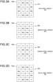
- FIGS. 3A to 3D are diagrams each illustrating an example of sensitivity of pixels according to an embodiment of the present disclosure.
- FIGS. 3A to 3D are diagrams for describing variations in sensitivity of the pixels 100 in the pixel group.
- the sensitivity of the pixel 100 varies due to variations in manufacturing processes and an influence of the pixels 100 of another adjacent pixel group.
- FIG. 3A is a diagram illustrating variations in sensitivity of the red pixels 100a of the red pixel group 310.
- “Lo” represents relatively low sensitivity
- “Mid” represents medium sensitivity
- “Hi” represents relatively high sensitivity.
- the red pixels 100a at the center have low sensitivity
- the red pixels 100a at the corners have high sensitivity.
- the red pixels 100a at the sides have medium sensitivity.
- FIG. 3B is a diagram illustrating variations in sensitivity of the green pixels 100b of the green pixel group 320. As illustrated in the drawing, the green pixels 100b at the upper and lower sides have low sensitivity, and the eight green pixels 100b in the central lateral direction have relatively high sensitivity.
- FIG. 3C is a diagram illustrating variations in sensitivity of the green pixels 100c of the green pixel group 330. As illustrated in the drawing, the green pixels 100c at the right and left sides have low sensitivity, and the eight green pixels 100c in a central vertical direction have relatively high sensitivity.
- FIG. 3D is a diagram illustrating variations in sensitivity of the blue pixels 100d of the blue pixel group 340. As illustrated in the drawing, the blue pixels 100d at the center have low sensitivity, and the blue pixels 100d at the corners have high sensitivity. The blue pixels 100d at the sides have medium sensitivity.
- the sensitivity can be adjusted by adjusting the on-chip lens.
- the sensitivity can also be adjusted by arranging a light-shielding wall that shields incident light incident on the pixel 100 and adjusting the light-shielding wall. Next, an example of a case of adjusting the on-chip lens will be described.
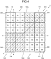
- FIG. 4 is a diagram illustrating a configuration example of pixels according to a first embodiment of the present disclosure.
- FIG. 4 is a plan view illustrating an example of on-chip lenses arranged in the pixel blocks.
- the on-chip lens is disposed for each pixel block.
- a region indicated by an alternate long and short dash line in the drawing represents an on-chip lens.
- the on-chip lens can have a substantially rectangular shape in plan view.
- the drawing illustrates an example in which the corners of the on-chip lens are configured by curves.
- the drawing illustrates an example in which the on-chip lens has a shape in contact with another adjacent on-chip lens is illustrated.
- An on-chip lens 171 is disposed in the red pixel group 310.
- An on-chip lens 172 is disposed in the green pixel block 220.
- An on-chip lens 173 is disposed in the green pixel block 230.
- An on-chip lens 174 is disposed in the blue pixel block 240.
- the on-chip lens 171 of the red pixel block 210 can have a shape protruding to the regions of the green pixel groups 320 and 330. That is, the on-chip lens 171 can have a shape covering the region of the pixels 100 of the adjacent green pixel groups 320 and 330.
- the on-chip lens 172 of the green pixel group 320 can have a shape protruding to the region of the blue pixel group 340.
- the on-chip lens 173 of the green pixel group 330 can have a shape protruding to the region of the blue pixel group 340.
- the on-chip lens 174 of the blue pixel group 340 can have a shape reduced inward of the pixel group.
- the on-chip lens 172 of the green pixel group 320 By forming the on-chip lens 172 of the green pixel group 320 in a shape protruding to the upper and lower regions of the blue pixel group 340, it is possible to widen a condensing range of the incident light of the green pixels 100b in the upper and lower side portions of the green pixel group 320, and to increase the sensitivity.
- the on-chip lens 172 of the green pixel group 320 is configured to be reduced in the right direction and the left direction adjacent to the red pixel group 310. As a result, the sensitivity of the green pixels 100b in the center of the left and right sides of the green pixel group 320 can be decreased. This makes it possible to reduce variations in sensitivity illustrated in FIG. 3B .
- the on-chip lens 173 of the green pixel group 330 By forming the on-chip lens 173 of the green pixel group 330 in a shape protruding to the regions of the left and right blue pixel groups 340, the light condensing range of the incident light of the green pixels 100c at the right and left sides of the green pixel group 330 can be widened, and the sensitivity can be increased.
- the on-chip lens 173 of the green pixel group 330 is configured to be reduced in the upper direction and the lower direction adjacent to the red pixel group 310. As a result, the sensitivity of the green pixels 100c in the center of the upper and lower sides of the green pixel group 330 can be decreased. This makes it possible to reduce variations in sensitivity illustrated in FIG. 3C .
- FIG. 5 is a diagram illustrating a configuration example of pixels according to the first embodiment of the present disclosure.
- the drawing is a sectional view illustrating a configuration example of the pixels 100.
- the drawing is a sectional view taken along line a-a' in FIG. 4 .
- the drawing illustrates the green pixels 100b of the green pixel block 220 of the green pixel group 320 and the blue pixels 100d of the blue pixel block 240 of the blue pixel group 340.
- the configuration of the pixel 100 will be described using the blue pixel 100d as an example.
- the blue pixel 100d includes a semiconductor substrate 120, a wiring region 140, a separator 131, and the color filter 164.
- the semiconductor substrate 120 is a semiconductor substrate on which a diffusion layer of a semiconductor element of the pixel 100 is disposed.
- the semiconductor substrate 120 can include, for example, silicon (Si).
- the semiconductor element and the like are disposed in a well region formed in the semiconductor substrate 120.
- the semiconductor substrate 120 in the drawing is assumed to be configured in a p-type well region.
- the semiconductor element can be formed by disposing an n-type or p-type semiconductor region in the p-type well region.
- a photoelectric converter 101 has been illustrated as an example on the semiconductor substrate 120 in the drawing.
- the photoelectric converter 101 includes an n-type semiconductor region 121.
- a photodiode including a pn junction at an interface between the n-type semiconductor region 121 and the surrounding p-type well region corresponds to the photoelectric converter 101.
- the wiring region 140 is a region that is disposed on a front surface of the semiconductor substrate 120 and in which wiring of an element is formed.
- the wiring region 140 is a region where wiring for transmitting a signal to an element or the like of the semiconductor substrate 120 is formed.
- the separator 131 is disposed at a boundary of the pixels 100 in the semiconductor substrate 120 to electrically and optically separate the pixel 100.
- the separator 131 can include an insulator embedded in the semiconductor substrate 120.
- the separator 131 can be formed, for example, by disposing an insulator such as SiO 2 in a groove penetrating the semiconductor substrate 120 formed at the boundary of the pixels 100. Note that the separator 131 can also have a shape reaching near the center of the semiconductor substrate 120 from a back surface of the semiconductor substrate 120 (not penetrating the semiconductor substrate 120).
- the color filter is an optical filter that transmits incident light having a predetermined wavelength among the incident light.
- a color filter that transmits red light, green light, and blue light can be used.
- the pixel 100 generates an image signal of incident light having a wavelength to which the color filter corresponds.
- the color filters 161, 162, 163, and 164 are respectively disposed in the red pixel 100a, the green pixel 100b, the green pixel 100c, and the blue pixel 100d.
- a light-shielding wall 150 is disposed in the region of the color filter at the boundary of the pixel group.
- the light-shielding wall 150 shields incident light. By arranging the light-shielding wall 150, it is possible to shield incident light obliquely incident from the adjacent pixel 100.
- the on-chip lens is a lens commonly disposed in the plurality of pixels 100 constituting the pixel block 210 and the like as described above.
- the on-chip lenses in the drawing has a hemispherical cross section and condenses incident light on a photoelectric converter.
- the on-chip lens can include an organic material such as an acrylic resin or an inorganic material such as silicon nitride (SiN).
- the on-chip lens 172 is disposed in the green pixel block 220, and the on-chip lens 174 is disposed in the blue pixel block 240.
- the on-chip lens 172 of the green pixel block 220 has a shape in which an end protrudes in the region of the blue pixel 100d of the blue pixel group 340.
- FIG. 6 is a diagram illustrating a configuration example of pixels according to the first embodiment of the present disclosure.
- the drawing is a sectional view illustrating a configuration example of the pixels 100, similarly to FIG. 5 .
- the drawing is a sectional view taken along line b-b' in FIG. 4 .
- the drawing illustrates the green pixels 100c of the green pixel block 230 of the green pixel group 330 and the blue pixels 100d of the blue pixel block 240 of the blue pixel group 340.
- the on-chip lens 173 of the green pixel block 230 has a shape in which an end protrudes in the region of the blue pixel 100d of the blue pixel group 340.
- FIG. 7 is a diagram illustrating a configuration example of pixels according to the first embodiment of the present disclosure.
- the drawing is a sectional view illustrating a configuration example of the pixels 100, similarly to FIG. 5 .
- the drawing is a sectional view taken along line c-c' in FIG. 4 .
- the drawing illustrates the red pixels 100a of the red pixel block 210 of the red pixel group 310 and the blue pixels 100d of the blue pixel block 240 of the blue pixel group 340.
- the on-chip lens 171 of the red pixel block 210 has a shape in which an end protrudes in the region of the blue pixel 100d of the blue pixel group 340.
- FIG. 8 is a diagram illustrating a configuration example of pixels according to the first embodiment of the present disclosure.
- the drawing is a sectional view illustrating a configuration example of the pixels 100, similarly to FIG. 5 .
- the drawing illustrates a configuration of the pixel 100 in a peripheral edge of the pixel array unit 11. Since the peripheral edge of the pixel array unit 11 has a high image height, the on-chip lens 172 and the like have a shape having a small curvature. In this manner, the curvature of the on-chip lens 172 and the like can be adjusted in accordance with the image height.
- FIG. 9 is a diagram illustrating another configuration example of pixels according to the first embodiment of the present disclosure.
- the drawing is a sectional view illustrating a configuration example of the pixels 100, similarly to FIG. 5 .
- the drawing illustrates an example of a case where the light-shielding wall 150 is disposed in the region of the color filter at a boundary of the pixel block (the pixel block 220 or the like). Note that the light-shielding wall 150 can also be disposed in the region of the color filter at the boundary of the pixels (the pixels 100b or the like).
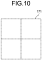
- FIG. 10 is a diagram illustrating another configuration example of an on-chip lens according to the first embodiment of the present disclosure.
- the drawing illustrates an example of an on-chip lens having a rectangular shape in plan view.
- the imaging element 10 adjusts the shape and the like of the on-chip lens for each pixel block. This makes it possible to reduce variations in sensitivity of the pixels 100 in the pixel group.
- the imaging element 10 according to the first embodiment described above uses an on-chip lens having a substantially rectangular shape.
- an imaging element 10 according to a second embodiment of the present disclosure is different from the first embodiment in that an on-chip lens provided with a recess is used.
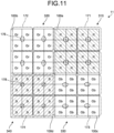
- FIG. 11 is a diagram illustrating a configuration example of pixels according to the second embodiment of the present disclosure.
- the drawing is a plan view illustrating an example of the on-chip lenses arranged in the pixel blocks.
- the on-chip lens 172 and the like in the drawing are different from the on-chip lens 172 and the like in FIG. 4 in that a recess 176 is disposed at a center.
- a condensing degree of the on-chip lens 172 and the like is adjusted. For example, in a pixel block having a large variation in sensitivity, the range of the recess 176 and the like of the on-chip lens is widened to reduce the condensing degree. This makes it possible to adjust variations in sensitivity of the pixels 100 in the pixel block.
- FIG. 12 is a diagram illustrating a configuration example of pixels according to the second embodiment of the present disclosure.
- the drawing is a sectional view illustrating a configuration example of the pixels 100, similarly to FIG. 5 .
- a recess 176 is disposed in the on-chip lens 172 in the drawing.
- a recess 178 is disposed in the on-chip lens 174 in the drawing.
- the configuration of the imaging element 10 other than the above configuration is similar to the configuration of the imaging element 10 according to the first embodiment of the present disclosure, and thus will not be described.
- variations in sensitivity can be further adjusted by forming the recess 176 and the like in the on-chip lens 172 and the like.
- the imaging element 10 according to the first embodiment described above adjusts the size of the on-chip lens in plan view.
- an imaging element 10 according to a third embodiment of the present disclosure is different from the first embodiment in that the height of the on-chip lens is adjusted.
- FIG. 13 is a diagram illustrating a configuration example of pixels according to the third embodiment of the present disclosure.
- the drawing illustrates the green pixels 100b of the green pixel block 220 of the green pixel group 320 and the red pixels 100a of the red pixel block 210 of the red pixel group 310.
- the on-chip lens 172 can have a lower height than the on-chip lens 171. By adjusting the height of the on-chip lens 172, a condensing spot can be adjusted, and the variation in sensitivity can be adjusted.
- FIG. 14 is a diagram illustrating a configuration example of pixels according to the third embodiment of the present disclosure.
- the drawing illustrates the green pixels 100c of the green pixel block 230 of the green pixel group 330 and the blue pixels 100d of the blue pixel block 240 of the blue pixel group 340.
- the on-chip lens 174 can have a lower height than the on-chip lens 173. Note that the on-chip lens 173 can have the same height as the on-chip lens 172.
- the configuration of the imaging element 10 other than the above configuration is similar to the configuration of the imaging element 10 according to the first embodiment of the present disclosure, and thus will not be described.
- the imaging element 10 according to the third embodiment of the present disclosure can further adjust the variation in sensitivity by adjusting the height of the on-chip lens 172 and the like.
- an imaging element 10 according to a fourth embodiment of the present disclosure is different from the first embodiment in that the light-shielding wall is adjusted.
- FIG. 15 is a diagram illustrating a configuration example of pixels according to the fourth embodiment of the present disclosure.
- the drawing is a plan view illustrating a configuration example of the pixels 100, similarly to FIG. 4 .
- the pixel 100 is different from the pixel in FIG. 4 in that a light-shielding wall 151 and the like are disposed in the red pixel group 310, the green pixel group 320, the green pixel group 330, and the blue pixel group 340 in FIG. 15 .
- the light-shielding wall 151 is disposed in the red pixel 100a in an outer periphery.
- the light-shielding wall 151 is a light-shielding wall having a width wider than the light-shielding wall 150 described in FIG. 5 in plan view.
- the light-shielding wall 151 can have a width of 20 nm.
- the sensitivity of the red pixels 100a in the outer periphery of the red pixel group 310 can be decreased.
- the light-shielding wall 153 is disposed in the center lateral direction.
- the light-shielding wall 153 can have the same width as the light-shielding wall 151.
- the light-shielding wall 154 is disposed in the central vertical direction.
- the light-shielding wall 154 can have the same width as the light-shielding wall 151.
- the light-shielding wall 152 is disposed in the blue pixel 100d in an outer periphery.
- the light-shielding wall 152 can also have the same width as the light-shielding wall 151.
- the light-shielding wall disposed between the red pixel group 310 and the green pixel groups 320 and 330 can have a shape protruding in the region of the red pixel group 310.
- the light-shielding wall disposed between the blue pixel group 340 and the green pixel groups 320 and 330 can have a shape protruding in the region of the blue pixel group 340.
- the light-shielding wall 153 in a direction perpendicular to a direction adjacent to the blue pixel group 340 is disposed at the center of the green pixel group 320, and the light-shielding wall 154 in a direction perpendicular to the direction adjacent to the blue pixel group 340 is disposed at the center of the green pixel group 330.
- These light-shielding walls can reduce variations in sensitivity of the pixel 100.
- FIG. 16 is a diagram illustrating a configuration example of pixels according to the fourth embodiment of the present disclosure.
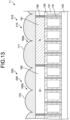
- the drawing is a sectional view illustrating a configuration example of the pixels 100, similarly to FIG. 5 .
- the drawing illustrates the green pixels 100b of the green pixel block 220 of the green pixel group 320 and the blue pixels 100d of the blue pixel block 240 of the blue pixel group 340.
- the light-shielding wall 153 is disposed at the center of the green pixel block 220 in the drawing.
- the light-shielding wall 152 is disposed at a peripheral edge of the blue pixel group 340 in the drawing.
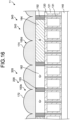
- FIG. 17 is a diagram illustrating a configuration example of pixels according to the fourth embodiment of the present disclosure.
- the drawing is a sectional view illustrating a configuration example of the pixels 100, similarly to FIG. 6 .
- the drawing illustrates the green pixels 100c of the green pixel block 230 of the green pixel group 330 and the blue pixels 100d of the blue pixel block 240 of the blue pixel group 340.
- the light-shielding wall 152 is disposed at the peripheral edge of the blue pixel group 340 in the drawing.
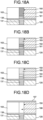
- FIGS. 18A to 18D are diagrams each illustrating a configuration example of the light-shielding wall according to the fourth embodiment of the present disclosure.
- the drawing is a sectional view illustrating a configuration example of the light-shielding wall 150. Note that the light-shielding walls 151 to 154 can also adopt a similar configuration.
- a protective film 139 is illustrated on the semiconductor substrate 120 in the drawing.
- FIG. 18A illustrates an example of the light-shielding wall 150 configured by stacking a light-shielding film 192 on a base 191.
- the base 191 can include titanium (Ti) or titanium nitride (TiN).
- the light-shielding film 192 in the drawing can include tungsten (W).
- FIG. 18B illustrates an example of the light-shielding wall 150 configured by stacking the base 191, the light-shielding film 192, and an oxide film 193.
- SiO 2 can be used for the oxide film 193.
- FIG. 18C illustrates an example of the light-shielding wall 150 configured by stacking bases 191 and 194 and a low refractive index member 195.
- FIG. 18D illustrates an example of the light-shielding wall 150 including a gap 196.
- a film 197 for sealing the gap 196 is disposed on the light-shielding wall 150 in the drawing.
- FIG. 19 is a diagram illustrating another configuration example of pixels according to the fourth embodiment of the present disclosure.
- the drawing illustrates an example in which a light-shielding wall is disposed around a pixel block.
- a light-shielding wall 155 is disposed between the adjacent red pixel blocks 210.
- the light-shielding wall 155 can have the same width as the light-shielding wall 150, for example.
- the light-shielding wall 155 is disposed in a portion where the light-shielding wall 153 is not disposed between the adjacent green pixel blocks 220.
- the light-shielding wall 155 is disposed in a portion where the light-shielding wall 154 is not disposed between the adjacent green pixel blocks 230.
- the light-shielding wall 155 is disposed between the adjacent blue pixel blocks 240.
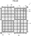
- FIG. 20 is a diagram illustrating another configuration example of pixels according to the fourth embodiment of the present disclosure.
- the drawing illustrates an example in which a light-shielding wall is disposed around a pixel.
- a light-shielding wall 156 is disposed between the adjacent red pixels 100a.
- the light-shielding wall 156 can have the same width as the light-shielding wall 150, for example.
- the green pixel block 220 in the drawing the light-shielding wall 156 is disposed between the adjacent green pixels 100b.
- the green pixel block 230 in the drawing the light-shielding wall 156 is disposed between the adjacent green pixels 100c.
- the blue pixel block 240 in the drawing the light-shielding wall 156 is disposed between the adjacent blue pixels 100d.
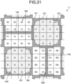
- FIG. 21 is a diagram illustrating another configuration example of pixels according to the fourth embodiment of the present disclosure.
- the drawing illustrates an example in which the width of the light-shielding wall is adjusted for each pixel 100 of the pixel group.
- the light-shielding wall 151 is disposed in the red pixel 100a at a corner of the red pixel group 310 in the drawing, and a light-shielding wall 157 is disposed in the red pixel 100a at a side.
- the light-shielding wall 157 can have the same width as the light-shielding wall 150, for example.
- the light-shielding wall 152 is disposed in the blue pixel 100d at a corner of the blue pixel group 340 in the drawing, and the light-shielding wall 157 is disposed in the blue pixel 100d at a side.
- the sensitivity of the blue pixels 100d disposed at the corners and the sides of the blue pixel group 340 can be individually adjusted.
- the configuration of the imaging element 10 other than the above configuration is similar to the configuration of the imaging element 10 according to the first embodiment of the present disclosure, and thus will not be described.
- the imaging element 10 adjusts the shape and the like of the light-shielding wall 151 and the like for each pixel block. This makes it possible to reduce variations in sensitivity of the pixels 100 in the pixel group.
- the imaging element 10 according to the first embodiment described above adjusts the shape and the like of the on-chip lens.
- an imaging element 10 according to a fifth embodiment of the present disclosure is different from the first embodiment in that the light-shielding wall is further adjusted.
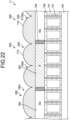
- FIG. 22 is a diagram illustrating a configuration example of pixels according to the fifth embodiment of the present disclosure.
- the drawing is a sectional view illustrating a configuration example of the pixels 100, similarly to FIG. 6 .
- the drawing illustrates the green pixels 100c of the green pixel block 230 of the green pixel group 330 and the blue pixels 100d of the blue pixel block 240 of the blue pixel group 340.
- the on-chip lens 172 in the drawing can also have a shape protruding to the region of the blue pixel group 340.
- the light-shielding wall 152 having a shape projecting in the region of the blue pixel group 340 can be disposed.
- the configuration of the imaging element 10 other than the above configuration is similar to the configuration of the imaging element 10 according to the first embodiment of the present disclosure, and thus will not be described.
- the imaging element 10 can reduce variations in sensitivity of the pixels 100 in the pixel group by adjusting the on-chip lens and the light-shielding wall.
Landscapes
- Engineering & Computer Science (AREA)
- Multimedia (AREA)
- Signal Processing (AREA)
- Physics & Mathematics (AREA)
- Spectroscopy & Molecular Physics (AREA)
- Color Television Image Signal Generators (AREA)
- Solid State Image Pick-Up Elements (AREA)
- Transforming Light Signals Into Electric Signals (AREA)
Abstract
Description
- The present disclosure relates to an imaging element and an imaging device.
- In an imaging element configured by arranging a plurality of pixels, an imaging element configured by arranging, in a Bayer array, a pixel group in which a plurality of pixels having color filters of the same color are arranged adjacent to each other has been proposed (see, for example, Patent Literature 1).
- Patent Literature 1:
US 2021/0144315 A - However, in the above conventional technique, there is a problem that a sensitivity difference between the pixels included in a unit cannot be adjusted, and an image quality is degraded.
- Therefore, the present disclosure proposes an imaging element and an imaging device that reduce a sensitivity difference between pixels in a pixel group in which a plurality of pixels having the same color filter are arranged adjacent to each other.
- The present disclosure has been conceived to solve the problem described above, and a first aspect thereof is an imaging element includes: a pixel array unit configured by arranging, in a Bayer array, a red pixel group in which red pixel blocks are arranged in two rows and two columns, a green pixel group in which green pixel blocks are arranged in two rows and two columns, and a blue pixel group in which blue pixel blocks are arranged in two rows and two columns, the red pixel blocks being configured by arranging, in two rows and two columns, red pixels that include a color filter transmitting red light, perform photoelectric conversion of incident light transmitted through the color filter, and generate an image signal corresponding to the red light and by arranging a common on-chip lens, the green pixel blocks being configured by arranging, in two rows and two columns, green pixels that include a color filter transmitting green light, perform photoelectric conversion of incident light transmitted through the color filter, and generate an image signal corresponding to the green light and by arranging a common on-chip lens, the blue pixel blocks being configured by arranging, in two rows and two columns, blue pixels that include a color filter transmitting blue light, perform photoelectric conversion of incident light transmitted through the color filter, and generate an image signal corresponding to the blue light and by arranging a common on-chip lens, wherein the common on-chip lens has a different shape for each of the red pixel group, the green pixel group, and the blue pixel group.
- Furthermore, a second aspect of the present disclosure is an imaging device includes: a pixel array unit configured by arranging, in a Bayer array, a red pixel group in which red pixel blocks are arranged in two rows and two columns, a green pixel group in which green pixel blocks are arranged in two rows and two columns, and a blue pixel group in which blue pixel blocks are arranged in two rows and two columns, the red pixel blocks being configured by arranging, in two rows and two columns, red pixels that include a color filter transmitting red light, perform photoelectric conversion of incident light transmitted through the color filter, and generate an image signal corresponding to the red light and by arranging a common on-chip lens, the green pixel blocks being configured by arranging, in two rows and two columns, green pixels that include a color filter transmitting green light, perform photoelectric conversion of incident light transmitted through the color filter, and generate an image signal corresponding to the green light and by arranging a common on-chip lens, the blue pixel blocks being configured by arranging, in two rows and two columns, blue pixels that include a color filter transmitting blue light, perform photoelectric conversion of incident light transmitted through the color filter, and generate an image signal corresponding to the blue light and by arranging a common on-chip lens; and a processing circuit that processes the image signal, wherein the common on-chip lens has a different shape for each of the red pixel group, the green pixel group, and the blue pixel group.
- Furthermore, a third aspect of the present disclosure is an imaging element includes: a pixel array unit configured by arranging, in a Bayer array, a red pixel group in which red pixel blocks are arranged in two rows and two columns, a green pixel group in which green pixel blocks are arranged in two rows and two columns, and a blue pixel group in which blue pixel blocks are arranged in two rows and two columns, the red pixel blocks being configured by arranging, in two rows and two columns, red pixels that include a color filter transmitting red light, perform photoelectric conversion of incident light transmitted through the color filter, and generate an image signal corresponding to the red light and by arranging a common on-chip lens, the green pixel blocks being configured by arranging, in two rows and two columns, green pixels that include a color filter transmitting green light, perform photoelectric conversion of incident light transmitted through the color filter, and generate an image signal corresponding to the green light and by arranging a common on-chip lens, the blue pixel blocks being configured by arranging, in two rows and two columns, blue pixels that include a color filter transmitting blue light, perform photoelectric conversion of incident light transmitted through the color filter, and generate an image signal corresponding to the blue light and by arranging a common on-chip lens; and a light-shielding wall disposed in a region of the color filter between the red pixel group, the green pixel group, and the blue pixel group, wherein the light-shielding wall has a different shape for each of the red pixel group, the green pixel group, and the blue pixel group.
- Furthermore, a fourth aspect of the present disclosure is an imaging device includes: a pixel array unit configured by arranging, in a Bayer array, a red pixel group in which red pixel blocks are arranged in two rows and two columns, a green pixel group in which green pixel blocks are arranged in two rows and two columns, and a blue pixel group in which blue pixel blocks are arranged in two rows and two columns, the red pixel blocks being configured by arranging, in two rows and two columns, red pixels that include a color filter transmitting red light, perform photoelectric conversion of incident light transmitted through the color filter, and generate an image signal corresponding to the red light and by arranging a common on-chip lens, the green pixel blocks being configured by arranging, in two rows and two columns, green pixels that include a color filter transmitting green light, perform photoelectric conversion of incident light transmitted through the color filter, and generate an image signal corresponding to the green light and by arranging a common on-chip lens, the blue pixel blocks being configured by arranging, in two rows and two columns, blue pixels that include a color filter transmitting blue light, perform photoelectric conversion of incident light transmitted through the color filter, and generate an image signal corresponding to the blue light and by arranging a common on-chip lens; a light-shielding wall disposed in a region of the color filter between the red pixel group, the green pixel group, and the blue pixel group; and a processing circuit that processes the image signal, wherein the light-shielding wall has a different shape for each of the red pixel group, the green pixel group, and the blue pixel group.
-
-
FIG. 1 is a diagram illustrating a configuration example of an imaging element according to an embodiment of the present disclosure. -
FIG. 2 is a diagram illustrating a configuration example of pixels according to an embodiment of the present disclosure. -
FIG. 3A is a diagram illustrating an example of sensitivity of pixels according to an embodiment of the present disclosure. -
FIG. 3B is a diagram illustrating an example of sensitivity of pixels according to an embodiment of the present disclosure. -
FIG. 3C is a diagram illustrating an example of sensitivity of pixels according to an embodiment of the present disclosure. -
FIG. 3D is a diagram illustrating an example of sensitivity of pixels according to an embodiment of the present disclosure. -
FIG. 4 is a diagram illustrating a configuration example of pixels according to a first embodiment of the present disclosure. -
FIG. 5 is a diagram illustrating a configuration example of pixels according to the first embodiment of the present disclosure. -
FIG. 6 is a diagram illustrating a configuration example of pixels according to the first embodiment of the present disclosure. -
FIG. 7 is a diagram illustrating a configuration example of pixels according to the first embodiment of the present disclosure. -
FIG. 8 is a diagram illustrating a configuration example of pixels according to a second embodiment of the present disclosure. -
FIG. 9 is a diagram illustrating another configuration example of pixels according to the first embodiment of the present disclosure. -
FIG. 10 is a diagram illustrating another configuration example of an on-chip lens according to the first embodiment of the present disclosure. -
FIG. 11 is a diagram illustrating a configuration example of pixels according to the second embodiment of the present disclosure. -
FIG. 12 is a diagram illustrating a configuration example of pixels according to the second embodiment of the present disclosure. -
FIG. 13 is a diagram illustrating a configuration example of pixels according to a third embodiment of the present disclosure. -
FIG. 14 is a diagram illustrating a configuration example of pixels according to the third embodiment of the present disclosure. -
FIG. 15 is a diagram illustrating a configuration example of pixels according to a fourth embodiment of the present disclosure. -
FIG. 16 is a diagram illustrating a configuration example of pixels according to the fourth embodiment of the present disclosure. -
FIG. 17 is a diagram illustrating a configuration example of pixels according to the fourth embodiment of the present disclosure. -
FIG. 18A is a diagram illustrating a configuration example of a light-shielding wall according to the fourth embodiment of the present disclosure. -
FIG. 18B is a diagram illustrating a configuration example of the light-shielding wall according to the fourth embodiment of the present disclosure. -
FIG. 18C is a diagram illustrating a configuration example of the light-shielding wall according to the fourth embodiment of the present disclosure. -
FIG. 18D is a diagram illustrating a configuration example of the light-shielding wall according to the fourth embodiment of the present disclosure. -
FIG. 19 is a diagram illustrating another configuration example of pixels according to the fourth embodiment of the present disclosure. -
FIG. 20 is a diagram illustrating another configuration example of pixels according to the fourth embodiment of the present disclosure. -
FIG. 21 is a diagram illustrating another configuration example of pixels according to the fourth embodiment of the present disclosure. -
FIG. 22 is a diagram illustrating a configuration example of pixels according to a fifth embodiment of the present disclosure. - Hereinafter, embodiments of the present disclosure will be described in detail with reference to the drawings. The description will be given in the following order. Note that, in the following embodiments, the same parts are denoted by the same reference signs, and redundant description will be omitted.
- 1. First embodiment
- 2. Second embodiment
- 3. Third embodiment
- 4. Fourth embodiment
- 5. Fifth embodiment
-
FIG. 1 is a diagram illustrating a configuration example of an imaging element according to an embodiment of the present disclosure. The drawing is a block diagram illustrating a configuration example of animaging element 10. Theimaging element 10 is a semiconductor element that generates image data of a subject. Theimaging element 10 includes apixel array unit 11, avertical drive unit 12, acolumn signal processor 13, and acontroller 14. - The
pixel array unit 11 is configured by arranging a plurality ofpixels 100. Thepixel array unit 11 in the drawing represents an example in which the plurality ofpixels 100 is arrayed in a shape of a two-dimensional matrix. Here, thepixel 100 includes a photoelectric converter that performs photoelectric conversion of incident light, and generates an image signal of a subject on the basis of emitted incident light. For example, a photodiode can be used as the photoelectric converter.Signal lines pixel 100. Thepixel 100 is controlled by a control signal transmitted by thesignal line 15 to generate an image signal, and outputs the generated image signal via thesignal line 16. Note that thesignal line 15 is arranged for each row in the shape of the two-dimensional matrix, and is commonly wired to the plurality ofpixels 100 arranged in one row. Thesignal line 16 is arranged for each column in the shape of the two-dimensional matrix, and is commonly wired to the plurality ofpixels 100 arranged in one column. - The
vertical drive unit 12 generates a control signal of thepixel 100 described above. Thevertical drive unit 12 in the drawing generates a control signal for each row of the two-dimensional matrix of thepixel array unit 11 and sequentially outputs the control signal via thesignal line 15. - The
column signal processor 13 processes the image signal generated by thepixel 100. Thecolumn signal processor 13 in the drawing simultaneously processes the image signals from the plurality ofpixels 100 arranged in one row of thepixel array unit 11 transmitted via thesignal line 16. As this processing, for example, analog-digital conversion of converting an analog image signal generated by thepixel 100 into a digital image signal and correlated double sampling (CDS) of removing an offset error of the image signal can be performed. The processed image signal is output to a circuit or the like outside theimaging element 10. - The
controller 14 controls thevertical drive unit 12 and thecolumn signal processor 13. Thecontroller 14 in the drawing generates a control signal for controlling thevertical drive unit 12 and thecolumn signal processor 13 on the basis of data for instructing a clock, an operation mode, and the like input from an external circuit or the like. Next, thecontroller 14 outputs control signals via thesignal lines vertical drive unit 12 and thecolumn signal processor 13. Note that thecolumn signal processor 13 is an example of a processing circuit described in the claims. -
FIG. 2 is a diagram illustrating a configuration example of pixels according to an embodiment of the present disclosure. The drawing is a plan view illustrating a configuration example of thepixels 100. As described above, thepixels 100 are arrayed in thepixel array unit 11. Thepixel array unit 11 in the drawing represents an example in which the plurality ofpixels 100 is arrayed in a two-dimensional matrix. Note that "R", "Gr", "Gb", and "B" attached to thepixels 100 in the drawing represent types of color filters to be described later. "R" in the drawing represents a color filter (color filter 161) corresponding to red light. "Gr" represents a color filter (color filter 162) corresponding to green light. "Gb" represents a color filter (color filter 163) corresponding to green light. "B" represents a color filter (color filter 164) corresponding to blue light. - The outlined rectangles in the drawing represent the
color filters color filter 161 corresponding to red light. A rectangle hatched diagonally in the upper right in the drawing represents thecolor filter 164 corresponding to blue light. - A rectangle in the drawing represents a region of the
pixel 100. A pixel in which thecolor filter 161 corresponding to red light is disposed is referred to as ared pixel 100a. The pixels in which thecolor filters green pixel 100b and agreen pixel 100c, respectively. A pixel in which thecolor filter 164 corresponding to blue light is disposed is referred to as ablue pixel 100d. - A plurality of adjacent pixels is collectively referred to as a pixel block. The color filter of the same color is disposed in the pixels of the pixel block. An on-chip lens to be described later is commonly disposed in the pixel block. The drawing illustrates an example of a pixel block including four
pixels 100 arranged in two rows and two columns. A pixel block configured by arranging thered pixels 100a in two rows and two columns is referred to as ared pixel block 210. Pixel blocks configured by arranging thegreen pixels 100b and thegreen pixels 100c in two rows and two columns are referred to as agreen pixel block 220 and agreen pixel block 230, respectively. A pixel block configured by arranging theblue pixels 100d in two rows and two columns is referred to as ablue pixel block 240. Note that the pixel block can include n x n (an integer of two or more)pixels 100. - A plurality of adjacent pixel blocks is collectively referred to as a pixel group. The color filters of the same color are disposed in the pixels of the pixel group. The drawing illustrates an example of a pixel group including four pixel blocks arranged in two rows and two columns. A pixel group configured by arranging the red pixel blocks 210 in two rows and two columns is referred to as a
red pixel group 310. Pixel groups configured by arranging thegreen pixel block 220 and thegreen pixel block 230 in two rows and two columns are referred to as agreen pixel group 320 and agreen pixel group 330, respectively. A pixel group configured by arranging the blue pixel blocks 240 in two rows and two columns is referred to as ablue pixel group 340. Thered pixel group 310, thegreen pixel groups blue pixel group 340 are arranged in a Bayer array. Note that the pixel group can include n x n (n is an integer of two or more) pixel blocks. - The
imaging element 10 including thepixel array unit 11 in the drawing can adjust a resolution of an image to be captured. When an image signal for eachpixel 100 is output, the highest resolution can be obtained. When an image signal for each pixel block is output, a middle resolution is obtained. When an image signal for each pixel group is output, the lowest resolution can be obtained. Such a sensitivity difference between thepixels 100 in the pixel group becomes a problem in theimaging element 10. This is because an image quality when the resolution is switched is deteriorated. -
FIGS. 3A to 3D are diagrams each illustrating an example of sensitivity of pixels according to an embodiment of the present disclosure.FIGS. 3A to 3D are diagrams for describing variations in sensitivity of thepixels 100 in the pixel group. The sensitivity of thepixel 100 varies due to variations in manufacturing processes and an influence of thepixels 100 of another adjacent pixel group. -
FIG. 3A is a diagram illustrating variations in sensitivity of thered pixels 100a of thered pixel group 310. In the figure, "Lo" represents relatively low sensitivity, "Mid" represents medium sensitivity, and "Hi" represents relatively high sensitivity. As illustrated in the drawing, thered pixels 100a at the center have low sensitivity, and thered pixels 100a at the corners have high sensitivity. Thered pixels 100a at the sides have medium sensitivity. -
FIG. 3B is a diagram illustrating variations in sensitivity of thegreen pixels 100b of thegreen pixel group 320. As illustrated in the drawing, thegreen pixels 100b at the upper and lower sides have low sensitivity, and the eightgreen pixels 100b in the central lateral direction have relatively high sensitivity. -
FIG. 3C is a diagram illustrating variations in sensitivity of thegreen pixels 100c of thegreen pixel group 330. As illustrated in the drawing, thegreen pixels 100c at the right and left sides have low sensitivity, and the eightgreen pixels 100c in a central vertical direction have relatively high sensitivity. -
FIG. 3D is a diagram illustrating variations in sensitivity of theblue pixels 100d of theblue pixel group 340. As illustrated in the drawing, theblue pixels 100d at the center have low sensitivity, and theblue pixels 100d at the corners have high sensitivity. Theblue pixels 100d at the sides have medium sensitivity. - As described above, different variations in sensitivity occur in each pixel group. Therefore, the sensitivity is adjusted for each pixel group. The sensitivity can be adjusted by adjusting the on-chip lens. The sensitivity can also be adjusted by arranging a light-shielding wall that shields incident light incident on the
pixel 100 and adjusting the light-shielding wall. Next, an example of a case of adjusting the on-chip lens will be described. -
FIG. 4 is a diagram illustrating a configuration example of pixels according to a first embodiment of the present disclosure.FIG. 4 is a plan view illustrating an example of on-chip lenses arranged in the pixel blocks. As described above, the on-chip lens is disposed for each pixel block. A region indicated by an alternate long and short dash line in the drawing represents an on-chip lens. The on-chip lens can have a substantially rectangular shape in plan view. The drawing illustrates an example in which the corners of the on-chip lens are configured by curves. The drawing illustrates an example in which the on-chip lens has a shape in contact with another adjacent on-chip lens is illustrated. An on-chip lens 171 is disposed in thered pixel group 310. An on-chip lens 172 is disposed in thegreen pixel block 220. An on-chip lens 173 is disposed in thegreen pixel block 230. An on-chip lens 174 is disposed in theblue pixel block 240. - The on-
chip lens 171 of thered pixel block 210 can have a shape protruding to the regions of thegreen pixel groups chip lens 171 can have a shape covering the region of thepixels 100 of the adjacentgreen pixel groups chip lens 172 of thegreen pixel group 320 can have a shape protruding to the region of theblue pixel group 340. The on-chip lens 173 of thegreen pixel group 330 can have a shape protruding to the region of theblue pixel group 340. The on-chip lens 174 of theblue pixel group 340 can have a shape reduced inward of the pixel group. - By forming the on-
chip lens 172 of thegreen pixel group 320 in a shape protruding to the upper and lower regions of theblue pixel group 340, it is possible to widen a condensing range of the incident light of thegreen pixels 100b in the upper and lower side portions of thegreen pixel group 320, and to increase the sensitivity. The on-chip lens 172 of thegreen pixel group 320 is configured to be reduced in the right direction and the left direction adjacent to thered pixel group 310. As a result, the sensitivity of thegreen pixels 100b in the center of the left and right sides of thegreen pixel group 320 can be decreased. This makes it possible to reduce variations in sensitivity illustrated inFIG. 3B . - By forming the on-
chip lens 173 of thegreen pixel group 330 in a shape protruding to the regions of the left and rightblue pixel groups 340, the light condensing range of the incident light of thegreen pixels 100c at the right and left sides of thegreen pixel group 330 can be widened, and the sensitivity can be increased. The on-chip lens 173 of thegreen pixel group 330 is configured to be reduced in the upper direction and the lower direction adjacent to thered pixel group 310. As a result, the sensitivity of thegreen pixels 100c in the center of the upper and lower sides of thegreen pixel group 330 can be decreased. This makes it possible to reduce variations in sensitivity illustrated inFIG. 3C . -
FIG. 5 is a diagram illustrating a configuration example of pixels according to the first embodiment of the present disclosure. The drawing is a sectional view illustrating a configuration example of thepixels 100. The drawing is a sectional view taken along line a-a' inFIG. 4 . The drawing illustrates thegreen pixels 100b of thegreen pixel block 220 of thegreen pixel group 320 and theblue pixels 100d of theblue pixel block 240 of theblue pixel group 340. The configuration of thepixel 100 will be described using theblue pixel 100d as an example. Theblue pixel 100d includes asemiconductor substrate 120, awiring region 140, aseparator 131, and thecolor filter 164. - The
semiconductor substrate 120 is a semiconductor substrate on which a diffusion layer of a semiconductor element of thepixel 100 is disposed. Thesemiconductor substrate 120 can include, for example, silicon (Si). The semiconductor element and the like are disposed in a well region formed in thesemiconductor substrate 120. For convenience, thesemiconductor substrate 120 in the drawing is assumed to be configured in a p-type well region. The semiconductor element can be formed by disposing an n-type or p-type semiconductor region in the p-type well region. Aphotoelectric converter 101 has been illustrated as an example on thesemiconductor substrate 120 in the drawing. Thephotoelectric converter 101 includes an n-type semiconductor region 121. Specifically, a photodiode including a pn junction at an interface between the n-type semiconductor region 121 and the surrounding p-type well region corresponds to thephotoelectric converter 101. - The
wiring region 140 is a region that is disposed on a front surface of thesemiconductor substrate 120 and in which wiring of an element is formed. Thewiring region 140 is a region where wiring for transmitting a signal to an element or the like of thesemiconductor substrate 120 is formed. - The
separator 131 is disposed at a boundary of thepixels 100 in thesemiconductor substrate 120 to electrically and optically separate thepixel 100. Theseparator 131 can include an insulator embedded in thesemiconductor substrate 120. Theseparator 131 can be formed, for example, by disposing an insulator such as SiO2 in a groove penetrating thesemiconductor substrate 120 formed at the boundary of thepixels 100. Note that theseparator 131 can also have a shape reaching near the center of thesemiconductor substrate 120 from a back surface of the semiconductor substrate 120 (not penetrating the semiconductor substrate 120). - The color filter is an optical filter that transmits incident light having a predetermined wavelength among the incident light. As the color filter, for example, a color filter that transmits red light, green light, and blue light can be used. The
pixel 100 generates an image signal of incident light having a wavelength to which the color filter corresponds. As described above, thecolor filters red pixel 100a, thegreen pixel 100b, thegreen pixel 100c, and theblue pixel 100d. - Note that, in the
pixel 100 in the drawing, a light-shieldingwall 150 is disposed in the region of the color filter at the boundary of the pixel group. The light-shieldingwall 150 shields incident light. By arranging the light-shieldingwall 150, it is possible to shield incident light obliquely incident from theadjacent pixel 100. - The on-chip lens is a lens commonly disposed in the plurality of
pixels 100 constituting thepixel block 210 and the like as described above. The on-chip lenses in the drawing has a hemispherical cross section and condenses incident light on a photoelectric converter. The on-chip lens can include an organic material such as an acrylic resin or an inorganic material such as silicon nitride (SiN). As described above, the on-chip lens 172 is disposed in thegreen pixel block 220, and the on-chip lens 174 is disposed in theblue pixel block 240. - As illustrated in the drawing, the on-
chip lens 172 of thegreen pixel block 220 has a shape in which an end protrudes in the region of theblue pixel 100d of theblue pixel group 340. -
FIG. 6 is a diagram illustrating a configuration example of pixels according to the first embodiment of the present disclosure. The drawing is a sectional view illustrating a configuration example of thepixels 100, similarly toFIG. 5 . The drawing is a sectional view taken along line b-b' inFIG. 4 . The drawing illustrates thegreen pixels 100c of thegreen pixel block 230 of thegreen pixel group 330 and theblue pixels 100d of theblue pixel block 240 of theblue pixel group 340. - As illustrated in the drawing, the on-
chip lens 173 of thegreen pixel block 230 has a shape in which an end protrudes in the region of theblue pixel 100d of theblue pixel group 340. -
FIG. 7 is a diagram illustrating a configuration example of pixels according to the first embodiment of the present disclosure. The drawing is a sectional view illustrating a configuration example of thepixels 100, similarly toFIG. 5 . The drawing is a sectional view taken along line c-c' inFIG. 4 . The drawing illustrates thered pixels 100a of thered pixel block 210 of thered pixel group 310 and theblue pixels 100d of theblue pixel block 240 of theblue pixel group 340. - As illustrated in the drawing, the on-
chip lens 171 of thered pixel block 210 has a shape in which an end protrudes in the region of theblue pixel 100d of theblue pixel group 340. -
FIG. 8 is a diagram illustrating a configuration example of pixels according to the first embodiment of the present disclosure. The drawing is a sectional view illustrating a configuration example of thepixels 100, similarly toFIG. 5 . The drawing illustrates a configuration of thepixel 100 in a peripheral edge of thepixel array unit 11. Since the peripheral edge of thepixel array unit 11 has a high image height, the on-chip lens 172 and the like have a shape having a small curvature. In this manner, the curvature of the on-chip lens 172 and the like can be adjusted in accordance with the image height. -
FIG. 9 is a diagram illustrating another configuration example of pixels according to the first embodiment of the present disclosure. The drawing is a sectional view illustrating a configuration example of thepixels 100, similarly toFIG. 5 . The drawing illustrates an example of a case where the light-shieldingwall 150 is disposed in the region of the color filter at a boundary of the pixel block (thepixel block 220 or the like). Note that the light-shieldingwall 150 can also be disposed in the region of the color filter at the boundary of the pixels (thepixels 100b or the like). -
FIG. 10 is a diagram illustrating another configuration example of an on-chip lens according to the first embodiment of the present disclosure. The drawing illustrates an example of an on-chip lens having a rectangular shape in plan view. - As described above, the
imaging element 10 according to the first embodiment of the present disclosure adjusts the shape and the like of the on-chip lens for each pixel block. This makes it possible to reduce variations in sensitivity of thepixels 100 in the pixel group. - The
imaging element 10 according to the first embodiment described above uses an on-chip lens having a substantially rectangular shape. On the other hand, animaging element 10 according to a second embodiment of the present disclosure is different from the first embodiment in that an on-chip lens provided with a recess is used. -
FIG. 11 is a diagram illustrating a configuration example of pixels according to the second embodiment of the present disclosure. Similarly toFIG. 4 , the drawing is a plan view illustrating an example of the on-chip lenses arranged in the pixel blocks. The on-chip lens 172 and the like in the drawing are different from the on-chip lens 172 and the like inFIG. 4 in that arecess 176 is disposed at a center. - By forming the
recess 176 and the like in the on-chip lens 172 and the like, a condensing degree of the on-chip lens 172 and the like is adjusted. For example, in a pixel block having a large variation in sensitivity, the range of therecess 176 and the like of the on-chip lens is widened to reduce the condensing degree. This makes it possible to adjust variations in sensitivity of thepixels 100 in the pixel block. -
FIG. 12 is a diagram illustrating a configuration example of pixels according to the second embodiment of the present disclosure. The drawing is a sectional view illustrating a configuration example of thepixels 100, similarly toFIG. 5 . In the on-chip lens 172 in the drawing, arecess 176 is disposed. In the on-chip lens 174 in the drawing, arecess 178 is disposed. - The configuration of the
imaging element 10 other than the above configuration is similar to the configuration of theimaging element 10 according to the first embodiment of the present disclosure, and thus will not be described. - As described above, in the
imaging element 10 according to the second embodiment of the present disclosure, variations in sensitivity can be further adjusted by forming therecess 176 and the like in the on-chip lens 172 and the like. - The
imaging element 10 according to the first embodiment described above adjusts the size of the on-chip lens in plan view. On the other hand, animaging element 10 according to a third embodiment of the present disclosure is different from the first embodiment in that the height of the on-chip lens is adjusted. -
FIG. 13 is a diagram illustrating a configuration example of pixels according to the third embodiment of the present disclosure. The drawing illustrates thegreen pixels 100b of thegreen pixel block 220 of thegreen pixel group 320 and thered pixels 100a of thered pixel block 210 of thered pixel group 310. As illustrated in the drawing, the on-chip lens 172 can have a lower height than the on-chip lens 171. By adjusting the height of the on-chip lens 172, a condensing spot can be adjusted, and the variation in sensitivity can be adjusted. -
FIG. 14 is a diagram illustrating a configuration example of pixels according to the third embodiment of the present disclosure. The drawing illustrates thegreen pixels 100c of thegreen pixel block 230 of thegreen pixel group 330 and theblue pixels 100d of theblue pixel block 240 of theblue pixel group 340. As illustrated in the drawing, the on-chip lens 174 can have a lower height than the on-chip lens 173. Note that the on-chip lens 173 can have the same height as the on-chip lens 172. - The configuration of the
imaging element 10 other than the above configuration is similar to the configuration of theimaging element 10 according to the first embodiment of the present disclosure, and thus will not be described. - As described above, the
imaging element 10 according to the third embodiment of the present disclosure can further adjust the variation in sensitivity by adjusting the height of the on-chip lens 172 and the like. - In the
imaging element 10 according to the first embodiment described above, the on-chip lens is adjusted. On the other hand, animaging element 10 according to a fourth embodiment of the present disclosure is different from the first embodiment in that the light-shielding wall is adjusted. -
FIG. 15 is a diagram illustrating a configuration example of pixels according to the fourth embodiment of the present disclosure. The drawing is a plan view illustrating a configuration example of thepixels 100, similarly toFIG. 4 . Thepixel 100 is different from the pixel inFIG. 4 in that a light-shieldingwall 151 and the like are disposed in thered pixel group 310, thegreen pixel group 320, thegreen pixel group 330, and theblue pixel group 340 inFIG. 15 . - In the
red pixel group 310 in the drawing, the light-shieldingwall 151 is disposed in thered pixel 100a in an outer periphery. The light-shieldingwall 151 is a light-shielding wall having a width wider than the light-shieldingwall 150 described inFIG. 5 in plan view. For example, when the light-shieldingwall 150 has a width of 10 nm, the light-shieldingwall 151 can have a width of 20 nm. As a result, the sensitivity of thered pixels 100a in the outer periphery of thered pixel group 310 can be decreased. - In the
green pixel group 320 in the drawing, the light-shieldingwall 153 is disposed in the center lateral direction. The light-shieldingwall 153 can have the same width as the light-shieldingwall 151. By arranging the light-shieldingwall 153, the sensitivity of the eightgreen pixels 100b in the central lateral direction of thegreen pixel group 320 can be decreased. - In the
green pixel group 330 in the drawing, the light-shieldingwall 154 is disposed in the central vertical direction. The light-shieldingwall 154 can have the same width as the light-shieldingwall 151. By arranging the light-shieldingwall 154, the sensitivity of the eightgreen pixels 100c in the central vertical direction of thegreen pixel group 330 can be decreased. - In the
blue pixel group 340 in the drawing, the light-shieldingwall 152 is disposed in theblue pixel 100d in an outer periphery. The light-shieldingwall 152 can also have the same width as the light-shieldingwall 151. By arranging the light-shieldingwall 152, the sensitivity of theblue pixel 100d in the outer periphery of theblue pixel group 340 can be decreased. - As illustrated in the drawing, the light-shielding wall disposed between the
red pixel group 310 and thegreen pixel groups red pixel group 310. The light-shielding wall disposed between theblue pixel group 340 and thegreen pixel groups blue pixel group 340. The light-shieldingwall 153 in a direction perpendicular to a direction adjacent to theblue pixel group 340 is disposed at the center of thegreen pixel group 320, and the light-shieldingwall 154 in a direction perpendicular to the direction adjacent to theblue pixel group 340 is disposed at the center of thegreen pixel group 330. These light-shielding walls can reduce variations in sensitivity of thepixel 100. -
FIG. 16 is a diagram illustrating a configuration example of pixels according to the fourth embodiment of the present disclosure. The drawing is a sectional view illustrating a configuration example of thepixels 100, similarly toFIG. 5 . The drawing illustrates thegreen pixels 100b of thegreen pixel block 220 of thegreen pixel group 320 and theblue pixels 100d of theblue pixel block 240 of theblue pixel group 340. The light-shieldingwall 153 is disposed at the center of thegreen pixel block 220 in the drawing. The light-shieldingwall 152 is disposed at a peripheral edge of theblue pixel group 340 in the drawing. -
FIG. 17 is a diagram illustrating a configuration example of pixels according to the fourth embodiment of the present disclosure. The drawing is a sectional view illustrating a configuration example of thepixels 100, similarly toFIG. 6 . The drawing illustrates thegreen pixels 100c of thegreen pixel block 230 of thegreen pixel group 330 and theblue pixels 100d of theblue pixel block 240 of theblue pixel group 340. The light-shieldingwall 152 is disposed at the peripheral edge of theblue pixel group 340 in the drawing. -
FIGS. 18A to 18D are diagrams each illustrating a configuration example of the light-shielding wall according to the fourth embodiment of the present disclosure. The drawing is a sectional view illustrating a configuration example of the light-shieldingwall 150. Note that the light-shieldingwalls 151 to 154 can also adopt a similar configuration. Aprotective film 139 is illustrated on thesemiconductor substrate 120 in the drawing. -
FIG. 18A illustrates an example of the light-shieldingwall 150 configured by stacking a light-shieldingfilm 192 on abase 191. The base 191 can include titanium (Ti) or titanium nitride (TiN). The light-shieldingfilm 192 in the drawing can include tungsten (W). -
FIG. 18B illustrates an example of the light-shieldingwall 150 configured by stacking thebase 191, the light-shieldingfilm 192, and anoxide film 193. For example, SiO2 can be used for theoxide film 193. -
FIG. 18C illustrates an example of the light-shieldingwall 150 configured by stackingbases refractive index member 195. -
FIG. 18D illustrates an example of the light-shieldingwall 150 including agap 196. Afilm 197 for sealing thegap 196 is disposed on the light-shieldingwall 150 in the drawing. -
FIG. 19 is a diagram illustrating another configuration example of pixels according to the fourth embodiment of the present disclosure. The drawing illustrates an example in which a light-shielding wall is disposed around a pixel block. In thered pixel group 310 in the drawing, a light-shieldingwall 155 is disposed between the adjacent red pixel blocks 210. The light-shieldingwall 155 can have the same width as the light-shieldingwall 150, for example. In thegreen pixel group 320 in the drawing, the light-shieldingwall 155 is disposed in a portion where the light-shieldingwall 153 is not disposed between the adjacent green pixel blocks 220. In thegreen pixel group 330 in the drawing, the light-shieldingwall 155 is disposed in a portion where the light-shieldingwall 154 is not disposed between the adjacent green pixel blocks 230. In theblue pixel group 340 in the drawing, the light-shieldingwall 155 is disposed between the adjacent blue pixel blocks 240. -
FIG. 20 is a diagram illustrating another configuration example of pixels according to the fourth embodiment of the present disclosure. The drawing illustrates an example in which a light-shielding wall is disposed around a pixel. In thered pixel block 210 in the drawing, a light-shieldingwall 156 is disposed between the adjacentred pixels 100a. The light-shieldingwall 156 can have the same width as the light-shieldingwall 150, for example. In thegreen pixel block 220 in the drawing, the light-shieldingwall 156 is disposed between the adjacentgreen pixels 100b. In thegreen pixel block 230 in the drawing, the light-shieldingwall 156 is disposed between the adjacentgreen pixels 100c. In theblue pixel block 240 in the drawing, the light-shieldingwall 156 is disposed between the adjacentblue pixels 100d. -
FIG. 21 is a diagram illustrating another configuration example of pixels according to the fourth embodiment of the present disclosure. The drawing illustrates an example in which the width of the light-shielding wall is adjusted for eachpixel 100 of the pixel group. The light-shieldingwall 151 is disposed in thered pixel 100a at a corner of thered pixel group 310 in the drawing, and a light-shieldingwall 157 is disposed in thered pixel 100a at a side. As a result, the sensitivity of thered pixels 100a disposed at the corner and the side of thered pixel group 310 can be individually adjusted. The light-shieldingwall 157 can have the same width as the light-shieldingwall 150, for example. - The light-shielding
wall 152 is disposed in theblue pixel 100d at a corner of theblue pixel group 340 in the drawing, and the light-shieldingwall 157 is disposed in theblue pixel 100d at a side. As a result, the sensitivity of theblue pixels 100d disposed at the corners and the sides of theblue pixel group 340 can be individually adjusted. - The configuration of the
imaging element 10 other than the above configuration is similar to the configuration of theimaging element 10 according to the first embodiment of the present disclosure, and thus will not be described. - As described above, the
imaging element 10 according to the fourth embodiment of the present disclosure adjusts the shape and the like of the light-shieldingwall 151 and the like for each pixel block. This makes it possible to reduce variations in sensitivity of thepixels 100 in the pixel group. - The
imaging element 10 according to the first embodiment described above adjusts the shape and the like of the on-chip lens. On the other hand, animaging element 10 according to a fifth embodiment of the present disclosure is different from the first embodiment in that the light-shielding wall is further adjusted. -
FIG. 22 is a diagram illustrating a configuration example of pixels according to the fifth embodiment of the present disclosure. The drawing is a sectional view illustrating a configuration example of thepixels 100, similarly toFIG. 6 . The drawing illustrates thegreen pixels 100c of thegreen pixel block 230 of thegreen pixel group 330 and theblue pixels 100d of theblue pixel block 240 of theblue pixel group 340. The on-chip lens 172 in the drawing can also have a shape protruding to the region of theblue pixel group 340. In thegreen pixel group 320 in the drawing, the light-shieldingwall 152 having a shape projecting in the region of theblue pixel group 340 can be disposed. - The configuration of the
imaging element 10 other than the above configuration is similar to the configuration of theimaging element 10 according to the first embodiment of the present disclosure, and thus will not be described. - As described above, the
imaging element 10 according to the fifth embodiment of the present disclosure can reduce variations in sensitivity of thepixels 100 in the pixel group by adjusting the on-chip lens and the light-shielding wall. - Although the embodiments of the present disclosure have been described above, the technical scope of the present disclosure is not limited to the above embodiments as it is, and various modifications can be made without departing from the gist of the present disclosure. The constituent elements of different embodiments and modifications may be appropriately combined.
- Note that the effects described in this specification are merely examples and are not limited, and other effects may be provided.
- Note that the present technique can also have the following configurations.
- (1) An imaging element comprising:
- a pixel array unit configured by arranging, in a Bayer array, a red pixel group in which red pixel blocks are arranged in two rows and two columns, a green pixel group in which green pixel blocks are arranged in two rows and two columns, and a blue pixel group in which blue pixel blocks are arranged in two rows and two columns, the red pixel blocks being configured by arranging, in two rows and two columns, red pixels that include a color filter transmitting red light, perform photoelectric conversion of incident light transmitted through the color filter, and generate an image signal corresponding to the red light and by arranging a common on-chip lens, the green pixel blocks being configured by arranging, in two rows and two columns, green pixels that include a color filter transmitting green light, perform photoelectric conversion of incident light transmitted through the color filter, and generate an image signal corresponding to the green light and by arranging a common on-chip lens, the blue pixel blocks being configured by arranging, in two rows and two columns, blue pixels that include a color filter transmitting blue light, perform photoelectric conversion of incident light transmitted through the color filter, and generate an image signal corresponding to the blue light and by arranging a common on-chip lens, wherein
- the common on-chip lens has a different shape for each of the red pixel group, the green pixel group, and the blue pixel group.
- (2) The imaging element according to the above (1), wherein the common on-chip lens has a different size in plan view for each of the red pixel group, the green pixel group, and the blue pixel group.
- (3) The imaging element according to the above (1) or (2), wherein the common on-chip lens of the red pixel group has a shape protruding to a region of the green pixel group.
- (4) The imaging element according to any one of the above (1) to (3), wherein the common on-chip lens of the green pixel group has a shape protruding to a region of the blue pixel group.
- (5) The imaging element according to any one of the above (1) to (4), wherein the common on-chip lens has a different height in plan view for each of the red pixel group, the green pixel group, and the blue pixel group.
- (6) The imaging element according to any one of the above (1) to (5), wherein a recess is provided at a center of the common on-chip lens.
- (7) The imaging element according to any one of the above (1) to (6), wherein the common on-chip lens has a substantially rectangular shape.
- (8) The imaging element according to the above (7), wherein the common on-chip lens has a shape in contact with another adjacent on-chip lens.
- (9) An imaging device comprising:
- a pixel array unit configured by arranging, in a Bayer array, a red pixel group in which red pixel blocks are arranged in two rows and two columns, a green pixel group in which green pixel blocks are arranged in two rows and two columns, and a blue pixel group in which blue pixel blocks are arranged in two rows and two columns, the red pixel blocks being configured by arranging, in two rows and two columns, red pixels that include a color filter transmitting red light, perform photoelectric conversion of incident light transmitted through the color filter, and generate an image signal corresponding to the red light and by arranging a common on-chip lens, the green pixel blocks being configured by arranging, in two rows and two columns, green pixels that include a color filter transmitting green light, perform photoelectric conversion of incident light transmitted through the color filter, and generate an image signal corresponding to the green light and by arranging a common on-chip lens, the blue pixel blocks being configured by arranging, in two rows and two columns, blue pixels that include a color filter transmitting blue light, perform photoelectric conversion of incident light transmitted through the color filter, and generate an image signal corresponding to the blue light and by arranging a common on-chip lens; and
- a processing circuit that processes the image signal, wherein
- the common on-chip lens has a different shape for each of the red pixel group, the green pixel group, and the blue pixel group.
- (10) An imaging element comprising:
- a pixel array unit configured by arranging, in a Bayer array, a red pixel group in which red pixel blocks are arranged in two rows and two columns, a green pixel group in which green pixel blocks are arranged in two rows and two columns, and a blue pixel group in which blue pixel blocks are arranged in two rows and two columns, the red pixel blocks being configured by arranging, in two rows and two columns, red pixels that include a color filter transmitting red light, perform photoelectric conversion of incident light transmitted through the color filter, and generate an image signal corresponding to the red light and by arranging a common on-chip lens, the green pixel blocks being configured by arranging, in two rows and two columns, green pixels that include a color filter transmitting green light, perform photoelectric conversion of incident light transmitted through the color filter, and generate an image signal corresponding to the green light and by arranging a common on-chip lens, the blue pixel blocks being configured by arranging, in two rows and two columns, blue pixels that include a color filter transmitting blue light, perform photoelectric conversion of incident light transmitted through the color filter, and generate an image signal corresponding to the blue light and by arranging a common on-chip lens; and
- a light-shielding wall disposed in a region of the color filter between the red pixel group, the green pixel group, and the blue pixel group, wherein
- the light-shielding wall has a different shape for each of the red pixel group, the green pixel group, and the blue pixel group.
- (11) The imaging element according to the above (10), wherein the light-shielding wall disposed between the red pixel group and the green pixel group has a shape protruding in a region of the red pixel group.
- (12) The imaging element according to the above (11), wherein among the light-shielding walls disposed between the red pixel group and the green pixel group, the light-shielding wall adjacent to the green pixel at a corner of the red pixel group has a shape protruding to the region of the red pixel group.
- (13) The imaging element according to the above (10), wherein the light-shielding wall disposed between the blue pixel group and the green pixel group has a shape protruding in a region of the blue pixel group.
- (14) The imaging element according to the above (13), wherein among the light-shielding walls disposed between the blue pixel group and the green pixel group, the light-shielding wall adjacent to the green pixel at a corner of the blue pixel group has a shape protruding to the region of the blue pixel group.
- (15) The imaging element according to (10), wherein the light-shielding wall having a width different from a width of the red pixel disposed at a side is disposed in the red pixel disposed at a corner in the red pixel disposed in an outer periphery of the red pixel group, and the light-shielding wall having a width different from a width of the blue pixel disposed at a side is disposed in the blue pixel disposed at a corner in the blue pixel disposed in an outer periphery of the blue pixel group.
- (16) The imaging element according to any one of the above (10) to (15), wherein the light-shielding wall in a direction perpendicular to a direction adjacent to the blue pixel group is further disposed at a center of the green pixel group.
- (17) The imaging element according to any one of the above (10) to (16), further comprising a second light-shielding wall disposed around each of the red pixels, the green pixels, and the blue pixels and having a narrower width than the light-shielding wall.
- (18) The imaging element according to any one of the above (10) to (17), wherein the light-shielding wall includes an oxide film.
- (19) The imaging element according to any one of the above (10) to (17), wherein the light-shielding wall includes a low refractive index member.
- (20) The imaging element according to the above (19), wherein the light-shielding wall includes a gap.
- (21) An imaging device comprising:
- a pixel array unit configured by arranging, in a Bayer array, a red pixel group in which red pixel blocks are arranged in two rows and two columns, a green pixel group in which green pixel blocks are arranged in two rows and two columns, and a blue pixel group in which blue pixel blocks are arranged in two rows and two columns, the red pixel blocks being configured by arranging, in two rows and two columns, red pixels that include a color filter transmitting red light, perform photoelectric conversion of incident light transmitted through the color filter, and generate an image signal corresponding to the red light and by arranging a common on-chip lens, the green pixel blocks being configured by arranging, in two rows and two columns, green pixels that include a color filter transmitting green light, perform photoelectric conversion of incident light transmitted through the color filter, and generate an image signal corresponding to the green light and by arranging a common on-chip lens, the blue pixel blocks being configured by arranging, in two rows and two columns, blue pixels that include a color filter transmitting blue light, perform photoelectric conversion of incident light transmitted through the color filter, and generate an image signal corresponding to the blue light and by arranging a common on-chip lens;
- a light-shielding wall disposed in a region of the color filter between the red pixel group, the green pixel group, and the blue pixel group; and
- a processing circuit that processes the image signal, wherein
- the light-shielding wall has a different shape for each of the red pixel group, the green pixel group, and the blue pixel group.
-
- 10 IMAGING ELEMENT
- 11 PIXEL ARRAY UNIT
- 13 COLUMN SIGNAL PROCESSOR
- 100 PIXEL
- 100a RED PIXEL
- 100b, 100c GREEN PIXEL
- 100d BLUE PIXEL
- 150 to 157 LIGHT-SHIELDING WALL
- 161 to 164 COLOR FILTER
- 171 to 174 ON-CHIP LENS
- 176, 178 RECESS
- 210 RED PIXEL BLOCK
- 220, 230 GREEN PIXEL BLOCK
- 240 BLUE PIXEL BLOCK
- 310 RED PIXEL GROUP
- 320, 330 GREEN PIXEL GROUP
- 340 BLUE PIXEL GROUP
Claims (21)
- An imaging element comprising:a pixel array unit configured by arranging, in a Bayer array, a red pixel group in which red pixel blocks are arranged in two rows and two columns, a green pixel group in which green pixel blocks are arranged in two rows and two columns, and a blue pixel group in which blue pixel blocks are arranged in two rows and two columns, the red pixel blocks being configured by arranging, in two rows and two columns, red pixels that include a color filter transmitting red light, perform photoelectric conversion of incident light transmitted through the color filter, and generate an image signal corresponding to the red light and by arranging a common on-chip lens, the green pixel blocks being configured by arranging, in two rows and two columns, green pixels that include a color filter transmitting green light, perform photoelectric conversion of incident light transmitted through the color filter, and generate an image signal corresponding to the green light and by arranging a common on-chip lens, the blue pixel blocks being configured by arranging, in two rows and two columns, blue pixels that include a color filter transmitting blue light, perform photoelectric conversion of incident light transmitted through the color filter, and generate an image signal corresponding to the blue light and by arranging a common on-chip lens, whereinthe common on-chip lens has a different shape for each of the red pixel group, the green pixel group, and the blue pixel group.
- The imaging element according to claim 1, wherein the common on-chip lens has a different size in plan view for each of the red pixel group, the green pixel group, and the blue pixel group.
- The imaging element according to claim 1, wherein the common on-chip lens of the red pixel group has a shape protruding to a region of the green pixel group.
- The imaging element according to claim 1, wherein the common on-chip lens of the green pixel group has a shape protruding to a region of the blue pixel group.
- The imaging element according to claim 1, wherein the common on-chip lens has a different height in plan view for each of the red pixel group, the green pixel group, and the blue pixel group.
- The imaging element according to claim 1, wherein a recess is provided at a center of the common on-chip lens.
- The imaging element according to claim 1, wherein the common on-chip lens has a substantially rectangular shape.
- The imaging element according to claim 7, wherein the common on-chip lens has a shape in contact with another adjacent on-chip lens.
- An imaging device comprising:a pixel array unit configured by arranging, in a Bayer array, a red pixel group in which red pixel blocks are arranged in two rows and two columns, a green pixel group in which green pixel blocks are arranged in two rows and two columns, and a blue pixel group in which blue pixel blocks are arranged in two rows and two columns, the red pixel blocks being configured by arranging, in two rows and two columns, red pixels that include a color filter transmitting red light, perform photoelectric conversion of incident light transmitted through the color filter, and generate an image signal corresponding to the red light and by arranging a common on-chip lens, the green pixel blocks being configured by arranging, in two rows and two columns, green pixels that include a color filter transmitting green light, perform photoelectric conversion of incident light transmitted through the color filter, and generate an image signal corresponding to the green light and by arranging a common on-chip lens, the blue pixel blocks being configured by arranging, in two rows and two columns, blue pixels that include a color filter transmitting blue light, perform photoelectric conversion of incident light transmitted through the color filter, and generate an image signal corresponding to the blue light and by arranging a common on-chip lens; anda processing circuit that processes the image signal, whereinthe common on-chip lens has a different shape for each of the red pixel group, the green pixel group, and the blue pixel group.
- An imaging element comprising:a pixel array unit configured by arranging, in a Bayer array, a red pixel group in which red pixel blocks are arranged in two rows and two columns, a green pixel group in which green pixel blocks are arranged in two rows and two columns, and a blue pixel group in which blue pixel blocks are arranged in two rows and two columns, the red pixel blocks being configured by arranging, in two rows and two columns, red pixels that include a color filter transmitting red light, perform photoelectric conversion of incident light transmitted through the color filter, and generate an image signal corresponding to the red light and by arranging a common on-chip lens, the green pixel blocks being configured by arranging, in two rows and two columns, green pixels that include a color filter transmitting green light, perform photoelectric conversion of incident light transmitted through the color filter, and generate an image signal corresponding to the green light and by arranging a common on-chip lens, the blue pixel blocks being configured by arranging, in two rows and two columns, blue pixels that include a color filter transmitting blue light, perform photoelectric conversion of incident light transmitted through the color filter, and generate an image signal corresponding to the blue light and by arranging a common on-chip lens; anda light-shielding wall disposed in a region of the color filter between the red pixel group, the green pixel group, and the blue pixel group, whereinthe light-shielding wall has a different shape for each of the red pixel group, the green pixel group, and the blue pixel group.
- The imaging element according to claim 10, wherein the light-shielding wall disposed between the red pixel group and the green pixel group has a shape protruding in a region of the red pixel group.
- The imaging element according to claim 11, wherein among the light-shielding walls disposed between the red pixel group and the green pixel group, the light-shielding wall adjacent to the green pixel at a corner of the red pixel group has a shape protruding to the region of the red pixel group.
- The imaging element according to claim 10, wherein the light-shielding wall disposed between the blue pixel group and the green pixel group has a shape protruding in a region of the blue pixel group.
- The imaging element according to claim 13, wherein among the light-shielding walls disposed between the blue pixel group and the green pixel group, the light-shielding wall adjacent to the green pixel at a corner of the blue pixel group has a shape protruding to the region of the blue pixel group.
- The imaging element according to claim 10, wherein the light-shielding wall having a width different from a width of the red pixel disposed at a side is disposed in the red pixel disposed at a corner in the red pixel disposed in an outer periphery of the red pixel group, and the light-shielding wall having a width different from a width of the blue pixel disposed at a side is disposed in the blue pixel disposed at a corner in the blue pixel disposed in an outer periphery of the blue pixel group.
- The imaging element according to claim 10, wherein the light-shielding wall in a direction perpendicular to a direction adjacent to the blue pixel group is further disposed at a center of the green pixel group.
- The imaging element according to claim 10, further comprising a second light-shielding wall disposed around each of the red pixels, the green pixels, and the blue pixels and having a narrower width than the light-shielding wall.
- The imaging element according to claim 10, wherein the light-shielding wall includes an oxide film.
- The imaging element according to claim 10, wherein the light-shielding wall includes a low refractive index member.
- The imaging element according to claim 19, wherein the light-shielding wall includes a gap.
- An imaging device comprising:a pixel array unit configured by arranging, in a Bayer array, a red pixel group in which red pixel blocks are arranged in two rows and two columns, a green pixel group in which green pixel blocks are arranged in two rows and two columns, and a blue pixel group in which blue pixel blocks are arranged in two rows and two columns, the red pixel blocks being configured by arranging, in two rows and two columns, red pixels that include a color filter transmitting red light, perform photoelectric conversion of incident light transmitted through the color filter, and generate an image signal corresponding to the red light and by arranging a common on-chip lens, the green pixel blocks being configured by arranging, in two rows and two columns, green pixels that include a color filter transmitting green light, perform photoelectric conversion of incident light transmitted through the color filter, and generate an image signal corresponding to the green light and by arranging a common on-chip lens, the blue pixel blocks being configured by arranging, in two rows and two columns, blue pixels that include a color filter transmitting blue light, perform photoelectric conversion of incident light transmitted through the color filter, and generate an image signal corresponding to the blue light and by arranging a common on-chip lens;a light-shielding wall disposed in a region of the color filter between the red pixel group, the green pixel group, and the blue pixel group; anda processing circuit that processes the image signal, whereinthe light-shielding wall has a different shape for each of the red pixel group, the green pixel group, and the blue pixel group.
Applications Claiming Priority (2)
| Application Number | Priority Date | Filing Date | Title |
|---|---|---|---|
| JP2022050590 | 2022-03-25 | ||
| PCT/JP2023/005628 WO2023181735A1 (en) | 2022-03-25 | 2023-02-17 | Imaging element and imaging device |
Publications (2)
| Publication Number | Publication Date |
|---|---|
| EP4503641A1 true EP4503641A1 (en) | 2025-02-05 |
| EP4503641A4 EP4503641A4 (en) | 2025-09-24 |
Family
ID=88101167
Family Applications (1)
| Application Number | Title | Priority Date | Filing Date |
|---|---|---|---|
| EP23774334.9A Pending EP4503641A4 (en) | 2022-03-25 | 2023-02-17 | IMAGING ELEMENT AND IMAGING DEVICE |
Country Status (7)
| Country | Link |
|---|---|
| US (1) | US12615447B2 (en) |
| EP (1) | EP4503641A4 (en) |
| JP (1) | JPWO2023181735A1 (en) |
| KR (1) | KR20240166529A (en) |
| CN (1) | CN118715783A (en) |
| TW (1) | TW202408223A (en) |
| WO (1) | WO2023181735A1 (en) |
Family Cites Families (17)
| Publication number | Priority date | Publication date | Assignee | Title |
|---|---|---|---|---|
| JP2006269735A (en) * | 2005-03-24 | 2006-10-05 | Sony Corp | Solid-state imaging device and method for manufacturing solid-state imaging device |
| JP4212605B2 (en) * | 2006-05-12 | 2009-01-21 | シャープ株式会社 | Image sensor and method for manufacturing image sensor |
| JP4212606B2 (en) * | 2006-05-12 | 2009-01-21 | シャープ株式会社 | Manufacturing method of imaging device |
| JP4968893B2 (en) | 2006-09-14 | 2012-07-04 | キヤノン株式会社 | Imaging device and imaging system |
| FR2929478B1 (en) * | 2008-03-28 | 2011-04-01 | St Microelectronics Sa | IMAGE SENSOR WITH IMPROVED SENSITIVITY |
| KR101012235B1 (en) * | 2008-09-04 | 2011-02-08 | 주식회사 동부하이텍 | Image sensor and its manufacturing method |
| JP5702625B2 (en) * | 2011-02-22 | 2015-04-15 | ソニー株式会社 | Image sensor, image sensor manufacturing method, pixel design method, and electronic device |
| JP6233188B2 (en) | 2013-12-12 | 2017-11-22 | ソニー株式会社 | Solid-state imaging device, manufacturing method thereof, and electronic device |
| US10680022B2 (en) | 2013-12-12 | 2020-06-09 | Sony Corporation | Solid state imaging device, manufacturing method of the same, and electronic equipment |
| JP2015153975A (en) * | 2014-02-18 | 2015-08-24 | ソニー株式会社 | Solid state image sensor, manufacturing method of the same, and electronic apparatus |
| JP6237431B2 (en) | 2014-04-15 | 2017-11-29 | ソニー株式会社 | Focus detection device, electronic equipment |
| CN113363268A (en) * | 2014-12-18 | 2021-09-07 | 索尼公司 | Imaging device and mobile apparatus |
| WO2019035374A1 (en) | 2017-08-18 | 2019-02-21 | ソニー株式会社 | Image pickup element and image pickup device |
| KR102501604B1 (en) | 2017-11-22 | 2023-02-17 | 소니 세미컨덕터 솔루션즈 가부시키가이샤 | Solid-state imaging element and electronic device |
| JP6970595B2 (en) * | 2017-11-24 | 2021-11-24 | ブリルニクス シンガポール プライベート リミテッド | Solid-state image sensor, manufacturing method of solid-state image sensor, and electronic equipment |
| JP6607275B2 (en) * | 2018-03-28 | 2019-11-20 | ソニー株式会社 | Solid-state imaging device and electronic device |
| KR102721299B1 (en) | 2019-11-12 | 2024-10-25 | 삼성전자주식회사 | Image senosor, image device having the same, and operating method therof |
-
2023
- 2023-02-17 KR KR1020247034659A patent/KR20240166529A/en active Pending
- 2023-02-17 US US18/846,379 patent/US12615447B2/en active Active
- 2023-02-17 JP JP2024509849A patent/JPWO2023181735A1/ja active Pending
- 2023-02-17 CN CN202380021830.XA patent/CN118715783A/en active Pending
- 2023-02-17 WO PCT/JP2023/005628 patent/WO2023181735A1/en not_active Ceased
- 2023-02-17 EP EP23774334.9A patent/EP4503641A4/en active Pending
- 2023-03-07 TW TW112108200A patent/TW202408223A/en unknown
Also Published As
| Publication number | Publication date |
|---|---|
| CN118715783A (en) | 2024-09-27 |
| WO2023181735A1 (en) | 2023-09-28 |
| KR20240166529A (en) | 2024-11-26 |
| JPWO2023181735A1 (en) | 2023-09-28 |
| EP4503641A4 (en) | 2025-09-24 |
| TW202408223A (en) | 2024-02-16 |
| US12615447B2 (en) | 2026-04-28 |
| US20250203228A1 (en) | 2025-06-19 |
Similar Documents
| Publication | Publication Date | Title |
|---|---|---|
| US10818722B2 (en) | Solid-state imaging device, method of manufacturing a solid-state imaging device, and electronic apparatus | |
| KR102577844B1 (en) | Image sensor | |
| KR102622057B1 (en) | Image sensor | |
| US20170077164A1 (en) | Solid-state image sensor and image pickup apparatus | |
| US9780131B1 (en) | Image sensor having grid pattern | |
| US20200075660A1 (en) | Solid-state image pickup device | |
| KR20230093074A (en) | Semiconductor device and electronic apparatus | |
| KR20160139266A (en) | Image sensor and electronic device having the same | |
| US12402428B2 (en) | Method for manufacturing light detection device, light detection device, and electronic device | |
| US20200075644A1 (en) | Solid-state imaging device | |
| CN113542639A (en) | Solid-state imaging device, manufacturing method of solid-state imaging device, and electronic device | |
| US9837454B2 (en) | Image sensor | |
| US20210183929A1 (en) | Image sensing device | |
| US20220173138A1 (en) | Solid-state image sensor | |
| US20230230992A1 (en) | Solid-state imaging device and electronic device | |
| KR102857608B1 (en) | Image Sensor | |
| US12433043B2 (en) | Imaging device including multiple photoelectric conversion layers, multiple pixel electrodes and plugs connecting substrate and the pixel electrodes | |
| US11817468B2 (en) | Image sensing device | |
| KR20240070262A (en) | Image sensing device | |
| US12615447B2 (en) | Imaging element and imaging device | |
| KR20250037890A (en) | Image sensor and method for fabricating the same | |
| US20250040277A1 (en) | Image sensor | |
| US20260107593A1 (en) | Image sensing device | |
| JP2024080697A (en) | Image Sensing Device | |
| JP2024095569A (en) | Image Sensing Device |
Legal Events
| Date | Code | Title | Description |
|---|---|---|---|
| STAA | Information on the status of an ep patent application or granted ep patent |
Free format text: STATUS: THE INTERNATIONAL PUBLICATION HAS BEEN MADE |
|
| PUAI | Public reference made under article 153(3) epc to a published international application that has entered the european phase |
Free format text: ORIGINAL CODE: 0009012 |
|
| STAA | Information on the status of an ep patent application or granted ep patent |
Free format text: STATUS: REQUEST FOR EXAMINATION WAS MADE |
|
| 17P | Request for examination filed |
Effective date: 20241015 |
|
| AK | Designated contracting states |
Kind code of ref document: A1 Designated state(s): AL AT BE BG CH CY CZ DE DK EE ES FI FR GB GR HR HU IE IS IT LI LT LU LV MC ME MK MT NL NO PL PT RO RS SE SI SK SM TR |
|
| DAV | Request for validation of the european patent (deleted) | ||
| DAX | Request for extension of the european patent (deleted) | ||
| A4 | Supplementary search report drawn up and despatched |
Effective date: 20250826 |
|
| RIC1 | Information provided on ipc code assigned before grant |
Ipc: H04N 25/13 20230101AFI20250820BHEP Ipc: H10F 39/00 20250101ALI20250820BHEP Ipc: H04N 23/55 20230101ALI20250820BHEP |