EP4503416A1 - Power conversion apparatus and energy storage apparatus - Google Patents
Power conversion apparatus and energy storage apparatus Download PDFInfo
- Publication number
- EP4503416A1 EP4503416A1 EP24189017.7A EP24189017A EP4503416A1 EP 4503416 A1 EP4503416 A1 EP 4503416A1 EP 24189017 A EP24189017 A EP 24189017A EP 4503416 A1 EP4503416 A1 EP 4503416A1
- Authority
- EP
- European Patent Office
- Prior art keywords
- bridge arm
- arm switch
- circuit
- switch
- voltage
- Prior art date
- Legal status (The legal status is an assumption and is not a legal conclusion. Google has not performed a legal analysis and makes no representation as to the accuracy of the status listed.)
- Pending
Links
Images






Classifications
-
- H—ELECTRICITY
- H02—GENERATION; CONVERSION OR DISTRIBUTION OF ELECTRIC POWER
- H02M—APPARATUS FOR CONVERSION BETWEEN AC AND AC, BETWEEN AC AND DC, OR BETWEEN DC AND DC, AND FOR USE WITH MAINS OR SIMILAR POWER SUPPLY SYSTEMS; CONVERSION OF DC OR AC INPUT POWER INTO SURGE OUTPUT POWER; CONTROL OR REGULATION THEREOF
- H02M3/00—Conversion of DC power input into DC power output
- H02M3/22—Conversion of DC power input into DC power output with intermediate conversion into AC
- H02M3/24—Conversion of DC power input into DC power output with intermediate conversion into AC by static converters
- H02M3/28—Conversion of DC power input into DC power output with intermediate conversion into AC by static converters using discharge tubes with control electrode or semiconductor devices with control electrode to produce the intermediate AC
- H02M3/325—Conversion of DC power input into DC power output with intermediate conversion into AC by static converters using discharge tubes with control electrode or semiconductor devices with control electrode to produce the intermediate AC using devices of a triode or a transistor type requiring continuous application of a control signal
- H02M3/335—Conversion of DC power input into DC power output with intermediate conversion into AC by static converters using discharge tubes with control electrode or semiconductor devices with control electrode to produce the intermediate AC using devices of a triode or a transistor type requiring continuous application of a control signal using semiconductor devices only
- H02M3/3353—Conversion of DC power input into DC power output with intermediate conversion into AC by static converters using discharge tubes with control electrode or semiconductor devices with control electrode to produce the intermediate AC using devices of a triode or a transistor type requiring continuous application of a control signal using semiconductor devices only having at least two simultaneously operating switches on the input side, e.g. "double forward" or "double (switched) flyback" converter
-
- H—ELECTRICITY
- H02—GENERATION; CONVERSION OR DISTRIBUTION OF ELECTRIC POWER
- H02M—APPARATUS FOR CONVERSION BETWEEN AC AND AC, BETWEEN AC AND DC, OR BETWEEN DC AND DC, AND FOR USE WITH MAINS OR SIMILAR POWER SUPPLY SYSTEMS; CONVERSION OF DC OR AC INPUT POWER INTO SURGE OUTPUT POWER; CONTROL OR REGULATION THEREOF
- H02M1/00—Details of apparatus for conversion
- H02M1/38—Means for preventing simultaneous conduction of switches
-
- H—ELECTRICITY
- H02—GENERATION; CONVERSION OR DISTRIBUTION OF ELECTRIC POWER
- H02M—APPARATUS FOR CONVERSION BETWEEN AC AND AC, BETWEEN AC AND DC, OR BETWEEN DC AND DC, AND FOR USE WITH MAINS OR SIMILAR POWER SUPPLY SYSTEMS; CONVERSION OF DC OR AC INPUT POWER INTO SURGE OUTPUT POWER; CONTROL OR REGULATION THEREOF
- H02M3/00—Conversion of DC power input into DC power output
- H02M3/22—Conversion of DC power input into DC power output with intermediate conversion into AC
- H02M3/24—Conversion of DC power input into DC power output with intermediate conversion into AC by static converters
- H02M3/28—Conversion of DC power input into DC power output with intermediate conversion into AC by static converters using discharge tubes with control electrode or semiconductor devices with control electrode to produce the intermediate AC
- H02M3/325—Conversion of DC power input into DC power output with intermediate conversion into AC by static converters using discharge tubes with control electrode or semiconductor devices with control electrode to produce the intermediate AC using devices of a triode or a transistor type requiring continuous application of a control signal
- H02M3/335—Conversion of DC power input into DC power output with intermediate conversion into AC by static converters using discharge tubes with control electrode or semiconductor devices with control electrode to produce the intermediate AC using devices of a triode or a transistor type requiring continuous application of a control signal using semiconductor devices only
- H02M3/33569—Conversion of DC power input into DC power output with intermediate conversion into AC by static converters using discharge tubes with control electrode or semiconductor devices with control electrode to produce the intermediate AC using devices of a triode or a transistor type requiring continuous application of a control signal using semiconductor devices only having several active switching elements
- H02M3/33573—Full-bridge at primary side of an isolation transformer
-
- H—ELECTRICITY
- H02—GENERATION; CONVERSION OR DISTRIBUTION OF ELECTRIC POWER
- H02H—EMERGENCY PROTECTIVE CIRCUIT ARRANGEMENTS
- H02H3/00—Emergency protective circuit arrangements for automatic disconnection directly responsive to an undesired change from normal electric working condition with or without subsequent reconnection ; integrated protection
- H02H3/08—Emergency protective circuit arrangements for automatic disconnection directly responsive to an undesired change from normal electric working condition with or without subsequent reconnection ; integrated protection responsive to excess current
-
- H—ELECTRICITY
- H02—GENERATION; CONVERSION OR DISTRIBUTION OF ELECTRIC POWER
- H02H—EMERGENCY PROTECTIVE CIRCUIT ARRANGEMENTS
- H02H7/00—Emergency protective circuit arrangements specially adapted for specific types of electric machines or apparatus or for sectionalised protection of cable or line systems, and effecting automatic switching in the event of an undesired change from normal working conditions
- H02H7/10—Emergency protective circuit arrangements specially adapted for specific types of electric machines or apparatus or for sectionalised protection of cable or line systems, and effecting automatic switching in the event of an undesired change from normal working conditions for converters; for rectifiers
- H02H7/12—Emergency protective circuit arrangements specially adapted for specific types of electric machines or apparatus or for sectionalised protection of cable or line systems, and effecting automatic switching in the event of an undesired change from normal working conditions for converters; for rectifiers for static converters or rectifiers
- H02H7/122—Emergency protective circuit arrangements specially adapted for specific types of electric machines or apparatus or for sectionalised protection of cable or line systems, and effecting automatic switching in the event of an undesired change from normal working conditions for converters; for rectifiers for static converters or rectifiers for inverters, i.e. DC/AC converters
- H02H7/1225—Emergency protective circuit arrangements specially adapted for specific types of electric machines or apparatus or for sectionalised protection of cable or line systems, and effecting automatic switching in the event of an undesired change from normal working conditions for converters; for rectifiers for static converters or rectifiers for inverters, i.e. DC/AC converters responsive to internal faults, e.g. shoot-through
-
- H—ELECTRICITY
- H02—GENERATION; CONVERSION OR DISTRIBUTION OF ELECTRIC POWER
- H02H—EMERGENCY PROTECTIVE CIRCUIT ARRANGEMENTS
- H02H7/00—Emergency protective circuit arrangements specially adapted for specific types of electric machines or apparatus or for sectionalised protection of cable or line systems, and effecting automatic switching in the event of an undesired change from normal working conditions
- H02H7/22—Emergency protective circuit arrangements specially adapted for specific types of electric machines or apparatus or for sectionalised protection of cable or line systems, and effecting automatic switching in the event of an undesired change from normal working conditions for distribution gear, e.g. bus-bar systems; for switching devices
- H02H7/222—Emergency protective circuit arrangements specially adapted for specific types of electric machines or apparatus or for sectionalised protection of cable or line systems, and effecting automatic switching in the event of an undesired change from normal working conditions for distribution gear, e.g. bus-bar systems; for switching devices for switches
-
- H—ELECTRICITY
- H02—GENERATION; CONVERSION OR DISTRIBUTION OF ELECTRIC POWER
- H02J—ELECTRIC POWER NETWORKS; CIRCUIT ARRANGEMENTS OR SYSTEMS FOR SUPPLYING OR DISTRIBUTING ELECTRIC POWER; SYSTEMS FOR STORING ELECTRIC ENERGY
- H02J7/00—Circuit arrangements for charging or discharging batteries or for supplying loads from batteries
- H02J7/60—Circuit arrangements for charging or discharging batteries or for supplying loads from batteries including safety or protection arrangements
- H02J7/62—Circuit arrangements for charging or discharging batteries or for supplying loads from batteries including safety or protection arrangements against overcurrent
-
- H—ELECTRICITY
- H02—GENERATION; CONVERSION OR DISTRIBUTION OF ELECTRIC POWER
- H02J—ELECTRIC POWER NETWORKS; CIRCUIT ARRANGEMENTS OR SYSTEMS FOR SUPPLYING OR DISTRIBUTING ELECTRIC POWER; SYSTEMS FOR STORING ELECTRIC ENERGY
- H02J7/00—Circuit arrangements for charging or discharging batteries or for supplying loads from batteries
- H02J7/865—Battery or charger load switching, e.g. concurrent charging and load supply
-
- H—ELECTRICITY
- H02—GENERATION; CONVERSION OR DISTRIBUTION OF ELECTRIC POWER
- H02M—APPARATUS FOR CONVERSION BETWEEN AC AND AC, BETWEEN AC AND DC, OR BETWEEN DC AND DC, AND FOR USE WITH MAINS OR SIMILAR POWER SUPPLY SYSTEMS; CONVERSION OF DC OR AC INPUT POWER INTO SURGE OUTPUT POWER; CONTROL OR REGULATION THEREOF
- H02M1/00—Details of apparatus for conversion
- H02M1/08—Circuits specially adapted for the generation of control voltages for semiconductor devices incorporated in static converters
- H02M1/088—Circuits specially adapted for the generation of control voltages for semiconductor devices incorporated in static converters for the simultaneous control of series or parallel connected semiconductor devices
-
- H—ELECTRICITY
- H02—GENERATION; CONVERSION OR DISTRIBUTION OF ELECTRIC POWER
- H02M—APPARATUS FOR CONVERSION BETWEEN AC AND AC, BETWEEN AC AND DC, OR BETWEEN DC AND DC, AND FOR USE WITH MAINS OR SIMILAR POWER SUPPLY SYSTEMS; CONVERSION OF DC OR AC INPUT POWER INTO SURGE OUTPUT POWER; CONTROL OR REGULATION THEREOF
- H02M1/00—Details of apparatus for conversion
- H02M1/32—Means for protecting converters other than automatic disconnection
-
- H—ELECTRICITY
- H02—GENERATION; CONVERSION OR DISTRIBUTION OF ELECTRIC POWER
- H02M—APPARATUS FOR CONVERSION BETWEEN AC AND AC, BETWEEN AC AND DC, OR BETWEEN DC AND DC, AND FOR USE WITH MAINS OR SIMILAR POWER SUPPLY SYSTEMS; CONVERSION OF DC OR AC INPUT POWER INTO SURGE OUTPUT POWER; CONTROL OR REGULATION THEREOF
- H02M3/00—Conversion of DC power input into DC power output
- H02M3/22—Conversion of DC power input into DC power output with intermediate conversion into AC
- H02M3/24—Conversion of DC power input into DC power output with intermediate conversion into AC by static converters
- H02M3/28—Conversion of DC power input into DC power output with intermediate conversion into AC by static converters using discharge tubes with control electrode or semiconductor devices with control electrode to produce the intermediate AC
- H02M3/325—Conversion of DC power input into DC power output with intermediate conversion into AC by static converters using discharge tubes with control electrode or semiconductor devices with control electrode to produce the intermediate AC using devices of a triode or a transistor type requiring continuous application of a control signal
- H02M3/335—Conversion of DC power input into DC power output with intermediate conversion into AC by static converters using discharge tubes with control electrode or semiconductor devices with control electrode to produce the intermediate AC using devices of a triode or a transistor type requiring continuous application of a control signal using semiconductor devices only
- H02M3/33569—Conversion of DC power input into DC power output with intermediate conversion into AC by static converters using discharge tubes with control electrode or semiconductor devices with control electrode to produce the intermediate AC using devices of a triode or a transistor type requiring continuous application of a control signal using semiconductor devices only having several active switching elements
- H02M3/33571—Half-bridge at primary side of an isolation transformer
Definitions
- This application relates to the field of electronic technologies, and in particular, to a power conversion apparatus and an energy storage apparatus.
- a lithium battery has features such as high energy density and long cycle life, and therefore is widely used in the field of photovoltaic energy storage and electric vehicles.
- a battery needs to perform energy conversion by using a power conversion circuit.
- a circuit topology formed by a bridge arm such as a half-bridge circuit and a full-bridge circuit, is widely used in the power conversion circuit. If straight-through occurs on an upper transistor and a lower transistor that form the bridge arm, the entire bridge arm is short-circuited, and a large current is generated. This causes damage or even explosion of switching transistors.
- This application provides a power conversion apparatus and an energy storage apparatus, to avoid a bridge arm straight-through problem.
- an embodiment of this application provides a power conversion apparatus.
- the power conversion apparatus includes a direct current-direct current conversion circuit and a controller.
- the direct current-direct current conversion circuit includes a full-bridge circuit, the full-bridge circuit includes a first bridge arm and a second bridge arm that are connected in parallel, and each of the bridge arms includes an upper bridge arm switch and a lower bridge arm switch that are connected in series.
- the controller is coupled to each of the bridge arms.
- the controller may control turn-on/off of the upper bridge arm switch and the lower bridge arm switch of each of the bridge arms based on a voltage of a first connection point between the upper bridge arm switch and the lower bridge arm switch in the first bridge arm and a voltage of a second connection point between the upper bridge arm switch and the lower bridge arm switch in the second bridge arm. For example, when it is determined that the voltage of the first connection point and the voltage of the second connection point meet a specified control requirement, it indicates that a short-circuit problem does not occur on some bridge arm switches, and corresponding bridge arm switches may be driven according to a PWM drive signal sent by a control chip. To be specific, the corresponding bridge arm switches are controlled to switch between being turned on and being turned off.
- the corresponding bridge arm switch When it is determined that the voltage of the first connection point or the voltage of the second connection point does not meet the specified control requirement, it indicates that a short-circuit problem is very likely to occur in a bridge arm switch, and the corresponding bridge arm switch needs to be turned off. To be specific, the corresponding bridge arm switch is controlled to be turned off, to reduce a possibility that bridge arm straight-through occurs.
- the controller determines that at least one of the lower bridge arm switch of the first bridge arm and the upper bridge arm switch of the second bridge arm is short-circuited, and controls both the upper bridge arm switch of the first bridge arm and the lower bridge arm switch of the second bridge arm to be turned off, to avoid a possibility that bridge arm straight-through occurs.
- the controller determines that the lower bridge arm switch of the first bridge arm and the upper bridge arm switch of the second bridge arm are not short-circuited, and controls, based on a PWM drive signal sent by the control chip, the upper bridge arm switch of the first bridge arm and the lower bridge arm switch of the second bridge arm to be simultaneously turned on or turned off.
- the upper bridge arm switch of the first bridge arm and the lower bridge arm switch of the second bridge arm are controlled to be simultaneously turned on, and at a next moment, the upper bridge arm switch of the first bridge arm and the lower bridge arm switch of the second bridge arm are controlled to be simultaneously turned off.
- the controller determines that at least one of the upper bridge arm switch of the first bridge arm and the lower bridge arm switch of the second bridge arm is short-circuited, and controls both the upper bridge arm switch of the second bridge arm and the lower bridge arm switch of the first bridge arm to be turned off, to avoid a possibility that bridge arm straight-through occurs.
- the controller determines that the upper bridge arm switch of the first bridge arm and the lower bridge arm switch of the second bridge arm are not short-circuited, and controls, based on a PWM drive signal sent by the control chip, the upper bridge arm switch of the second bridge arm and the lower bridge arm switch of the first bridge arm to be simultaneously turned on or turned off.
- the upper bridge arm switch of the second bridge arm and the lower bridge arm switch of the first bridge arm are controlled to be simultaneously turned on, and at a next moment, the upper bridge arm switch of the second bridge arm and the lower bridge arm switch of the first bridge arm are controlled to be simultaneously turned off.
- an embodiment of this application provides another power conversion apparatus.
- the power conversion apparatus includes a direct current-direct current conversion circuit and a controller.
- the direct current-direct current conversion circuit includes a half-bridge circuit, the half-bridge circuit includes a first bridge arm, and the first bridge arm includes an upper bridge arm switch and a lower bridge arm switch that are connected in series.
- the controller is coupled to the first bridge arm. The controller may control turn-on/off of the upper bridge arm switch and the lower bridge arm switch of the first bridge arm based on a voltage of a first connection point between the upper bridge arm switch and the lower bridge arm switch in the first bridge arm.
- corresponding bridge arm switches may be driven according to a PWM drive signal sent by a control chip.
- the corresponding bridge arm switches are controlled to be turned on or turned off.
- the corresponding bridge arm switch is controlled to be turned off, to reduce a possibility that bridge arm straight-through occurs.
- the controller determines that the lower bridge arm switch of the first bridge arm is short-circuited, and controls the upper bridge arm switch to be turned off, to avoid a possibility that bridge arm straight-through occurs.
- the controller determines that the lower bridge arm switch of the first bridge arm is not short-circuited, and controls, based on a PWM drive signal sent by the control chip, the upper bridge arm switch to switch between being turned on and being turned off.
- the upper bridge arm switch is controlled to be turned on, and at a next moment, the upper bridge arm switch is controlled to be turned off.
- the controller determines that the lower bridge arm switch of the first bridge arm is short-circuited, and controls the lower bridge arm switch to be turned off, to avoid a possibility that bridge arm straight-through occurs.
- the controller determines that the lower bridge arm switch of the first bridge arm is not short-circuited, and controls, based on a PWM drive signal sent by the control chip, the lower bridge arm switch to switch between being turned on and being turned off.
- the lower bridge arm switch is controlled to be turned on, and at a next moment, the lower bridge arm switch is controlled to be turned off.
- an embodiment of this application provides another power conversion apparatus.
- the power conversion apparatus includes a direct current-direct current conversion circuit and a controller.
- the direct current-direct current conversion circuit includes an LLC circuit, the LLC circuit includes a first bridge arm and a second bridge arm that are connected in series, and each of the bridge arms includes an upper bridge arm switch and a lower bridge arm switch that are connected in series.
- the controller is coupled to each of the bridge arms. The controller may control turn-on/off of the upper bridge arm switch and the lower bridge arm switch of the first bridge arm based on a voltage of a first connection point between the upper bridge arm switch and the lower bridge arm switch in the first bridge arm.
- the controller may control turn-on/off of the upper bridge arm switch and the lower bridge arm switch of the second bridge arm based on a voltage of a second connection point between the upper bridge arm switch and the lower bridge arm switch in the second bridge arm. For example, when it is determined that the voltage of the first connection point or the voltage of the second connection point meets a specified control requirement, it indicates that a short-circuit problem does not occur on some bridge arm switches, and corresponding bridge arm switches may be driven according to a PWM drive signal sent by a control chip. To be specific, the corresponding bridge arm switches are controlled to switch between being turned on and being turned off.
- the corresponding bridge arm switch When it is determined that the voltage of the first connection point or the voltage of the second connection point does not meet the specified control requirement, it indicates that a short-circuit problem is very likely to occur in a bridge arm switch, and the corresponding bridge arm switch needs to be turned off. To be specific, the corresponding bridge arm switch is controlled to be turned off, to reduce a possibility that bridge arm straight-through occurs.
- the controller determines that the lower bridge arm switch of the first bridge arm is short-circuited, and controls the upper bridge arm switch of the first bridge arm to be turned off, to avoid a possibility that bridge arm straight-through occurs.
- the controller determines that the lower bridge arm switch of the first bridge arm is not short-circuited, and controls, based on a PWM drive signal sent by the control chip, the upper bridge arm switch of the first bridge arm to switch between being turned on and being turned off.
- the upper bridge arm switch of the first bridge arm is controlled to be turned on, and at a next moment, the upper bridge arm switch of the first bridge arm is controlled to be turned off.
- the controller determines that the upper bridge arm switch of the first bridge arm is short-circuited, and controls the lower bridge arm switch of the first bridge arm to be turned off, to avoid a possibility that bridge arm straight-through occurs.
- the controller determines that the upper bridge arm switch of the first bridge arm is not short-circuited, and controls, based on a PWM drive signal sent by the control chip, the lower bridge arm switch of the first bridge arm to switch between being turned on and being turned off.
- the lower bridge arm switch of the first bridge arm is controlled to be turned on, and at a next moment, the lower bridge arm switch of the first bridge arm is controlled to be turned off.
- the controller determines that the lower bridge arm switch of the second bridge arm is short-circuited, and controls the upper bridge arm switch of the second bridge arm to be turned off, to avoid a possibility that bridge arm straight-through occurs.
- the controller determines that the lower bridge arm switch of the second bridge arm is not short-circuited, and controls, based on a PWM drive signal sent by the control chip, the upper bridge arm switch of the second bridge arm to switch between being turned on and being turned off.
- the upper bridge arm switch of the second bridge arm is controlled to be turned on, and at a next moment, the upper bridge arm switch of the second bridge arm is controlled to be turned off.
- the controller determines that the upper bridge arm switch of the second bridge arm is short-circuited, and controls the lower bridge arm switch of the second bridge arm to be turned off, to avoid a possibility that bridge arm straight-through occurs.
- the controller determines that the upper bridge arm switch of the second bridge arm is not short-circuited, and controls, based on a PWM drive signal sent by the control chip, the lower bridge arm switch of the second bridge arm to switch between being turned on and being turned off.
- the lower bridge arm switch of the second bridge arm is controlled to be turned on, and at a next moment, the lower bridge arm switch of the second bridge arm is controlled to be turned off.
- an embodiment of this application further provides an energy storage apparatus, including a battery control unit, a plurality of battery packs, and a plurality of power conversion apparatuses according to any one of the first aspect to the third aspect.
- the plurality of battery packs are disposed in parallel, and each of the battery packs is connected to the battery control unit after being connected in series to one power conversion apparatus.
- the power conversion apparatus includes a primary-side circuit, a primary-side winding, a secondary-side winding, and a secondary-side circuit that are sequentially coupled.
- the secondary-side circuit is coupled to the battery pack.
- the secondary-side circuit may be a full-bridge circuit, a half-bridge circuit, or an LLC circuit.
- the controller in the power conversion apparatus may collect a voltage of a connection point between an upper bridge arm switch and a lower bridge arm switch in a bridge arm of the secondary-side circuit, and control turn-on/off of the upper bridge arm switch and the lower bridge arm switch in the corresponding bridge arm based on the voltage of the connection point, to reduce a possibility that bridge arm straight-through occurs, and prevent a battery pack short-circuit.
- 110 photovoltaic array
- 120 power converter
- 130 power grid
- 140 external load
- 150 energy storage apparatus
- 100 DC-DC conversion circuit
- 200 controller
- 300 battery
- 101 primary-side circuit
- Pr primary-side winding
- Sr secondary-side winding
- 102 secondary-side circuit
- 103 resonance circuit
- 210 first sampling circuit
- 220 second sampling circuit
- 230 logic circuit
- 240 drive circuit
- 231 first comparison circuit
- 232 second comparison circuit
- 233 third comparison circuit
- 234 fourth comparison circuit
- 235 first AND logic circuit
- 236 second AND logic circuit
- 237 third AND logic circuit
- 238 fourth AND logic circuit
- P1 first connection point
- P2 second connection point
- TA first bridge arm
- TB second bridge arm
- TC capacitor branch
- Q1 and Q3 upper bridge arm switches
- Q2 and Q4 lower bridge arm switches
- T1 first switching transistor
- T2 second switching transistor
- T3 third switching transistor
- T4 fourth switching transistor
- connection in embodiments of this application may be understood as an electric connection, and a connection between two electrical elements may be a direct or indirect connection between the two electrical elements.
- a connection between A and B may be a direct connection between A and B, or may be an indirect connection between A and B through one or more other electrical elements.
- a is connected to B may also be that A is directly connected to C, C is directly connected to B, A and B are connected through C.
- the "connection” may also be understood as coupling, for example, electromagnetic coupling between two inductors.
- the connection between A and B enables transmission of electric energy between A and B.
- the power conversion apparatus provided in embodiments of this application may be used in a scenario such as a photovoltaic system or an energy storage apparatus.
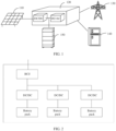
- FIG. 1 is an example of a schematic of a frame structure of a photovoltaic system.
- the photovoltaic system includes a photovoltaic array 110, a power converter 120, an energy storage apparatus 150, and a power grid 130 or an external load 140.
- the power converter 120 may integrate a DC/DC conversion circuit and a DC/AC conversion circuit.
- the energy storage apparatus 150 may be located between the DC/DC conversion circuit and the DC/AC conversion circuit. After the DC/DC conversion circuit performs boost or buck conversion on electric energy generated by the photovoltaic array 110, electric energy obtained after the conversion may be used to charge the energy storage apparatus 150.
- electric energy stored in the energy storage apparatus 150 may be transmitted to the power grid 130 or the external load 140 through the DC/AC conversion circuit in the power converter 120.
- the energy storage apparatus 150 may further receive power supply from the power grid 130, and an alternating current output by the power grid 130 is converted into a direct current by using the DC/AC conversion circuit, and then is transmitted to the energy storage apparatus 150, so as to charge the energy storage apparatus 150.
- FIG. 2 is an example schematic of a structure of an energy storage apparatus.
- the energy storage apparatus 150 may include a battery control unit (battery control unit, BCU), a plurality of battery packs, and a plurality of power conversion apparatuses.
- the power conversion apparatus includes a direct current (direct current, DC)-direct current conversion circuit (also referred to as a DC/DC conversion circuit or a DC-DC conversion circuit for short).
- the plurality of battery packs are disposed in parallel, and each of the battery pack is connected to the battery control unit after being connected to a DC-DC conversion circuit in series.
- the DC-DC conversion circuit may perform power conversion on electric energy stored in the battery pack and then output electric energy obtained after the conversion, or perform power conversion on external power supply and then store, in the battery pack, external power supply obtained after the conversion.
- FIG. 3 is an example schematic of a structure of a power conversion apparatus.
- the power conversion apparatus may further include a controller 200.
- the DC-DC conversion circuit 100 may include a primary-side circuit 101, a secondary-side circuit 102, and a transformer.
- the transformer usually includes a primary-side winding Pr and a secondary-side winding Sr.
- the primary-side circuit 101, the primary-side winding Pr, the secondary-side winding Sr, and the secondary-side circuit 102 may be sequentially coupled.
- a battery 300 (which may also be referred to as a battery pack) is usually coupled to the secondary-side circuit 102.
- the battery 300 may be coupled to the primary-side circuit 101.
- An example in which the battery 300 is coupled to the secondary-side circuit 102 is used for description below.
- the controller 200 is connected to the primary-side circuit 101 and the secondary-side circuit 102.
- the controller 200 may generate a plurality of control signals, for example, a pulse width modulation (pulse width modulation, PWM) signal, to control the primary-side circuit 101 and the secondary-side circuit 102 to work.
- PWM pulse width modulation
- the controller 200 may be any one of a microprocessor (microcontroller unit, MCU), a general-purpose central processing unit (central processing unit, CPU), a general-purpose processor, digital signal processing (digital signal processing, DSP), an application-specific integrated circuit (application-specific integrated circuit, ASIC), a field programmable gate array (field programmable gate array, FPGA), or the like inside the conversion circuit, or may be any one or a combination of another programmable logic device, a transistor logic device, or a hardware component.
- a plurality of power conversion apparatuses may share a same controller 200, or may be separately provided with different controllers 200.
- the controller 200 may be independently disposed, or may be integrated into another component, for example, may be integrated into a BCU.
- the controller 200 may control the DC-DC conversion circuit 100 to convert high-voltage direct-current electric energy into low-voltage direct-current electric energy, and output the low-voltage direct-current electric energy to the battery 300, to charge the battery 300.
- the primary-side circuit 101 may receive high-voltage direct-current electric energy, and the secondary-side circuit 102 may output low-voltage direct-current electric energy. Therefore, the primary-side circuit 101 may also be generally referred to as a high-voltage side circuit, and the secondary-side circuit 102 may also be generally referred to as a low-voltage side circuit.
- the controller 200 may control the DC-DC conversion circuit 100 to perform voltage conversion on direct-current electric energy stored in the battery 300, and then output electric energy obtained after the conversion, to discharge the battery 300.
- FIG. 4 is an example schematic of a specific circuit structure of a power conversion apparatus according to this application.
- Aprimary-side circuit 101 and a secondary-side circuit 102 in the power conversion apparatus may be implemented by using a full-bridge circuit topology, a half-bridge circuit topology, an LLC circuit topology, or another circuit topology.
- a full-bridge circuit topology and a half-bridge circuit topology may each include a bridge arm formed by a plurality of switches or switching transistors connected in series.
- one bridge arm may include an upper bridge arm switch and a lower bridge arm switch that are connected in series.
- the full-bridge circuit topology includes two bridge arms connected in parallel, and the half-bridge circuit topology includes one bridge arm and a capacitor connected in parallel.
- the upper bridge arm switch is usually located at an upper end of the bridge arm and is connected to a high-potential voltage terminal
- the lower bridge arm switch is usually located at a lower end of the bridge arm and is connected to a low-potential voltage terminal.
- a voltage value of the high-potential voltage terminal is higher than a voltage value of the low-potential voltage terminal.
- the high-potential voltage terminal may be an input voltage terminal Vin
- the low-potential voltage terminal may be a ground voltage.
- a high-potential voltage terminal connected to an upper bridge arm switch may be a positive terminal BAT+ of a battery 300, and a low-potential voltage terminal connected to a lower bridge arm switch may be a negative terminal BAT- of the battery 300.
- a high-potential voltage terminal connected to an upper bridge arm switch may be a high-voltage positive input terminal HV+, and a low-potential voltage terminal connected to a lower bridge arm switch may be a high-voltage negative input terminal HV-.
- switches or switching transistors in the primary-side circuit 101 and the secondary-side circuit 102 may be one or more of a plurality of types of switches such as a relay, a metal-oxide semiconductor field-effect transistor (metal-oxide semiconductor field-effect transistor, MOSFET), a bipolar junction transistor (bipolar junction transistor, BJT), and an insulated gate bipolar transistor (insulated gate bipolar transistor, IGBT). Details are not listed in this embodiment of this application.
- a switching transistor may include a first electrode, a second electrode, and a control electrode, and the control electrode is configured to control turn-on/off of the switching transistor. When the switching transistor is turned on, a current can be transmitted between the first electrode and the second electrode of the switching transistor.
- a control electrode of a switching transistor is a gate
- a first electrode of the switching transistor may be a source of the switching transistor
- a second electrode may be a drain of the switching transistor.
- the first electrode may be a drain of the switching transistor
- the second electrode may be a source of the switching transistor.
- the switching transistor and the switch in this embodiment of this application may be in an on state driven by a signal whose level is a first level, and may be in an off state driven by a signal whose level is a second level.
- the first level may be a high level
- the second level may be a low level.
- the first level is a low level
- the second level is a high level.
- the controller 200 is coupled to each bridge arm switch.
- the controller 200 may collect a voltage of a connection point between an upper bridge arm switch and a lower bridge arm switch in a bridge arm, and control turn-on/off of the upper bridge arm switch and the lower bridge arm switch in the corresponding bridge arm based on the voltage of the connection point. For example, when it is determined that the voltage of the connection point meets a specified control requirement, it indicates that there is no short-circuited switch in the bridge arm, and then a corresponding bridge arm switch may be driven according to a PWM drive signal sent by a control chip. To be specific, the corresponding bridge arm switch is controlled to switch between being turned on and being turned off.
- the controller 200 may perform the foregoing sampling control only on the primary-side circuit 101, to reduce a possibility that bridge-arm straight-through occurs in the primary-side circuit 101.
- the controller 200 may perform the foregoing sampling control only on the secondary-side circuit 102, to reduce a possibility that bridge-arm straight-through occurs in the secondary-side circuit 102.
- the controller 200 may separately perform the foregoing sampling control on the primary-side circuit 101 and the secondary-side circuit 102, to reduce a possibility that bridge-arm straight-through occurs in the primary-side circuit 101 and the secondary-side circuit 102.
- controller 200 controls a working mode of a corresponding bridge arm switch based on a voltage of a connection point of a bridge arm for different circuit topologies, to reduce a possibility that bridge arm straight-through occurs.
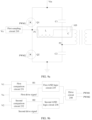
- FIG. 5 is an example schematic of specific circuit control of a full-bridge circuit in a power conversion apparatus according to this application.
- the full-bridge circuit may include a first bridge arm TA and a second bridge arm TB that are connected in parallel.
- the first bridge arm TA may include an upper bridge arm switch Q1 and a lower bridge arm switch Q2 that are connected in series.
- a first connection point P1 between the upper bridge arm switch Q1 and the lower bridge arm switch Q2 may be referred to as a midpoint of the first bridge arm TA.
- the second bridge arm TB may include an upper bridge arm switch Q3 and a lower bridge arm switch Q4 that are connected in series.
- a second connection point P2 between the upper bridge arm switch Q3 and the lower bridge arm switch Q4 may be referred to as a midpoint of the second bridge arm TB.
- the upper bridge arm switches Q1 and Q3 are both connected to an input voltage terminal Vin, and the lower bridge arm switches Q2 and Q4 are grounded after being connected.
- a positive terminal BAT+ of the battery may be used as an input voltage terminal Vin
- a negative terminal BAT- of the battery may be grounded
- a first terminal of a secondary-side winding Sr is coupled to the midpoint of the first bridge arm TA, namely, the first connection point P1
- a second terminal of the secondary-side winding Sr is coupled to the midpoint of the second bridge arm TB, namely, the second connection point P2.
- a high-voltage positive input terminal HV+ may be used as an input voltage terminal Vin
- a high-voltage negative input terminal HV- may be grounded
- a first terminal of a primary-side winding Pr is coupled to the midpoint of the first bridge arm TA, namely, the first connection point P1
- a second terminal of the primary-side winding Pr is coupled to the midpoint of the second bridge arm TB, namely, the second connection point P2.
- the controller 200 may be coupled to the first bridge arm TA and the second bridge arm TB of the full-bridge circuit.
- the controller 200 controls turn-on/off of the upper bridge arm switch Q1 of the first bridge arm TA and the lower bridge arm switch Q4 of the second bridge arm TB and turn-on/off of the upper bridge arm switch Q3 of the second bridge arm TB and the lower bridge arm switch Q2 of the first bridge arm TA based on a voltage of the first connection point P1 between the upper bridge arm switch Q1 and the lower bridge arm switch Q2 in the first bridge arm TA and a voltage of the second connection point P2 between the upper bridge arm switch Q3 and the lower bridge arm switch Q4 in the second bridge arm TB.
- the controller 200 may sample the voltages of the first connection point P1 and the second connection point P2. When it is determined that the voltage of the first connection point P1 is greater than the first threshold V1 and the voltage of the second connection point P2 is less than the second threshold V2, the controller determines that the lower bridge arm switch Q2 of the first bridge arm TA and the upper bridge arm switch Q3 of the second bridge arm TB are not short-circuited, and controls, based on a PWM drive signal sent by the control chip, the upper bridge arm switch Q1 of the first bridge arm TA and the lower bridge arm switch Q4 of the second bridge arm TB to simultaneously switch between being turned on and being turned off.
- the upper bridge arm switch Q1 of the first bridge arm TA and the lower bridge arm switch Q4 of the second bridge arm TB are controlled to be simultaneously turned on, and at a next moment, the upper bridge arm switch Q1 of the first bridge arm TA and the lower bridge arm switch Q4 of the second bridge arm TB are controlled to be simultaneously turned off.
- the controller determines that the upper bridge arm switch Q1 of the first bridge arm TA and the lower bridge arm switch Q4 of the second bridge arm TB are not short-circuited, and controls, based on a PWM drive signal sent by the control chip, the lower bridge arm switch Q2 of the first bridge arm TA and the upper bridge arm switch Q3 of the second bridge arm TB to simultaneously switch between being turned on and being turned off.
- the lower bridge arm switch Q2 of the first bridge arm TA and the upper bridge arm switch Q3 of the second bridge arm TB are controlled to be simultaneously turned on, and at a next moment, the lower bridge arm switch Q2 of the first bridge arm TA and the upper bridge arm switch Q3 of the second bridge arm TB are controlled to be simultaneously turned off.
- the controller determines that at least one of the lower bridge arm switch Q2 of the first bridge arm TA and the upper bridge arm switch Q3 of the second bridge arm TB is short-circuited, and may control both the upper bridge arm switch Q1 of the first bridge arm TA and the lower bridge arm switch Q4 of the second bridge arm TB to be turned off, to avoid a possibility that bridge arm straight-through occurs.
- the controller determines that at least one of the upper bridge arm switch Q1 of the first bridge arm TA and the lower bridge arm switch Q4 of the second bridge arm TB is short-circuited, and may control both the lower bridge arm switch Q2 of the first bridge arm TA and the upper bridge arm switch Q3 of the second bridge arm TB to be turned off, to avoid a possibility that bridge arm straight-through occurs.
- the first threshold V1 and the second threshold V2 may each be between 0 and Vin, in other words, 0 ⁇ V1 ⁇ Vin and 0 ⁇ V2 ⁇ Vin.
- the controller 200 may specifically include a first sampling circuit 210, a second sampling circuit 220, a logic circuit 230, and a drive circuit 240.
- the first sampling circuit 210 may sample the voltage of the first connection point P1 and output the voltage to the logic circuit 230
- the second sampling circuit 220 may sample the voltage of the second connection point P2 and output the voltage to the logic circuit 230.
- the logic circuit 230 may output a first enable signal to the drive circuit 240 based on a received first drive signal output by the chip, where the first enable signal is a necessary condition for turning on the upper bridge arm switch Q1 of the first bridge arm TA and the lower bridge arm switch Q4 of the second bridge arm TB.
- the logic circuit 230 may output a second enable signal to the drive circuit 240 based on a received second drive signal output by the chip, where the second enable signal is a necessary condition for turning on the lower bridge arm switch Q2 of the first bridge arm TA and the upper bridge arm switch Q3 of the second bridge arm TB.
- the drive circuit 240 may generate first PWM signals PWM1 and PWM4 and output the first PWM signals to the upper bridge arm switch Q1 of the first bridge arm TA and the lower bridge arm switch Q4 of the second bridge arm TB respectively.
- the drive circuit 240 may generate second PWM signals PWM2 and PWM3 and output the second PWM signals to the lower bridge arm switch Q2 of the first bridge arm TA and the upper bridge arm switch Q3 of the second bridge arm TB respectively.
- FIG. 6 is an example schematic of a specific circuit structure of a drive circuit in a power conversion apparatus according to this application.
- the logic circuit 230 may specifically include a first comparison circuit 231, a second comparison circuit 232, a third comparison circuit 233, a fourth comparison circuit 234, a first AND logic circuit 235, a second AND logic circuit 236, a third AND logic circuit 237, and a fourth AND logic circuit 238.
- the first comparison circuit 231 outputs a first high level signal H1 when it is determined that the voltage Va of the first connection point P1 is greater than the first threshold V1.
- the second comparison circuit 232 outputs a second high level signal H2 when it is determined that the voltage Va of the first connection point P1 is less than the second threshold V2.
- the third comparison circuit 233 outputs a third high level signal H3 when it is determined that the voltage Vb of the second connection point P2 is greater than the first threshold V1.
- the fourth comparison circuit 234 outputs a fourth high level signal H4 when it is determined that the voltage Vb of the second connection point P2 is less than the second threshold V2.
- the first AND logic circuit 235 receives the first high level signal H1 and the fourth high level signal H4 at the same time, it indicates that the voltage Va of the first connection point P1 is greater than the first threshold V1 and the voltage Vb of the second connection point P2 is less than the second threshold V2, and a fifth high level signal H5 is output.
- the second AND logic circuit 236 When the second AND logic circuit 236 receives the second high level signal H2 and the third high level signal H3 at the same time, it indicates that the voltage Va of the first connection point P1 is less than the second threshold V2 and the voltage Vb of the second connection point P2 is greater than the first threshold V1, and a sixth high level signal H6 is output.
- the third AND logic circuit 237 After receiving the fifth high level signal H5, the third AND logic circuit 237 may perform AND logic with the first drive signal output by the chip, to generate and output the first enable signal, so that the drive circuit 240 may generate the first PWM signal PWM1 after receiving the first enable signal, to drive the upper bridge arm switch Q1 of the first bridge arm TA and the lower bridge arm switch Q4 of the second bridge arm TB simultaneously.
- the fourth AND logic circuit 238 may perform AND logic with the second drive signal output by the chip, to generate and output the second enable signal, so that the drive circuit 240 may generate the second PWM signal PWM2 after receiving the second enable signal, to drive the lower bridge arm switch Q2 of the first bridge arm TA and the upper bridge arm switch Q3 of the second bridge arm TB simultaneously.
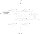
- FIG. 7a is an example schematic of a specific circuit structure of a full-bridge circuit in a power conversion apparatus according to this application.
- bridge arm switches Q1, Q2, Q3, and Q4 in the full-bridge circuit may each be implemented by using one switching transistor.
- the full-bridge circuit may be directly connected to a primary-side winding (or a secondary-side winding).
- FIG. 7b is an example schematic of another specific circuit structure of a full-bridge circuit in a power conversion apparatus according to this application.
- FIG. 7c is an example schematic of another specific circuit structure of a full-bridge circuit in a power conversion apparatus according to this application.
- a resonance circuit 103 may be further disposed between the full-bridge circuit and the primary-side winding (or the secondary-side winding).
- the resonance circuit 103 may be coupled between a first end of the primary-side winding (or the secondary-side winding) and a first connection point P1, or the resonance circuit 103 may be coupled between a second end of the primary-side winding (or the secondary-side winding) and a second connection point P2.
- the resonance circuit 103 may include an inductor L, so that the inductor L and the full-bridge circuit form a phase-shifted full-bridge circuit.
- the resonance circuit 103 may further include a capacitor C connected in series to the inductor L, so that the inductor L, the capacitor C, and the full-bridge circuit form an LLC/CLLC full-bridge circuit.
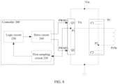
- FIG. 8 is an example schematic of specific circuit control of a half-bridge circuit in a power conversion apparatus according to this application.
- FIG. 8 is an example schematic of specific circuit control of a half-bridge circuit in a power conversion apparatus according to this application.
- the half-bridge circuit may include a first bridge arm TA.
- the first bridge arm TA may include an upper bridge arm switch Q1 and a lower bridge arm switch Q2 that are connected in series.
- a first connection point P1 between the upper bridge arm switch Q1 and the lower bridge arm switch Q2 may be referred to as a midpoint of the first bridge arm TA.
- the upper bridge arm switch Q1 is connected to an input voltage terminal Vin, and the lower bridge arm switch Q2 is grounded.
- the half-bridge circuit may further include a capacitor branch TC connected in parallel to the first bridge arm TA, and the capacitor branch TC may include a first capacitor C1 and a second capacitor C2 that are connected in series.
- a second connection point P2 between the first capacitor C1 and the second capacitor C2 may be referred to as a midpoint of the capacitor branch TC.
- a positive terminal BAT+ of the battery may be used as an input voltage terminal Vin
- a negative terminal BAT- of the battery may be grounded
- a first terminal of a secondary-side winding Sr is coupled to the midpoint of the first bridge arm TA, namely, the first connection point P1
- a second terminal of the secondary-side winding Sr is coupled to the midpoint of the capacitor branch TC, namely, the second connection point P2.
- a high-voltage positive input terminal HV+ may be used as an input voltage terminal Vin
- a high-voltage negative input terminal HV- may be grounded
- a first terminal of a primary-side winding Pr is coupled to the midpoint of the first bridge arm TA, namely, the first connection point P1
- a second terminal of the primary-side winding Pr is coupled to the midpoint of the capacitor branch TC, namely, the second connection point P2.
- the controller 200 may be coupled to the first bridge arm TA of the half-bridge circuit.
- the controller 200 controls turn-on/off of the upper bridge arm switch Q1 and the lower bridge arm switch Q2 of the first bridge arm TA based on a voltage of the first connection point P1 between the upper bridge arm switch Q1 and the lower bridge arm switch Q2 in the first bridge arm TA.
- the controller 200 may sample the voltage of the first connection point P1. When it is determined that the voltage of the first connection point P1 is greater than the first threshold V1, the controller determines that the lower bridge arm switch Q2 of the first bridge arm TA is not short-circuited, and may control, based on a PWM drive signal sent by the control chip, the upper bridge arm switch Q1 of the first bridge arm TA to switch between being turned on and being turned off. To be specific, at a moment, the upper bridge arm switch Q1 of the first bridge arm TA is controlled to be turned on, and at a next moment, the upper bridge arm switch Q1 of the first bridge arm TA is controlled to be turned off.
- the controller determines that the lower bridge arm switch Q2 of the first bridge arm TA is not short-circuited, and may control, based on a PWM drive signal sent by the control chip, the lower bridge arm switch Q2 of the first bridge arm TA to switch between being turned on and being turned off.
- the lower bridge arm switch Q2 of the first bridge arm TA is controlled to be turned on, and at a next moment, the lower bridge arm switch Q2 of the first bridge arm TA is controlled to be turned off.
- the controller determines that the lower bridge arm switch Q2 of the first bridge arm TA is short-circuited, and may control the upper bridge arm switch Q1 of the first bridge arm TA to be turned off, to avoid a possibility that bridge arm straight-through occurs.
- the controller determines that the lower bridge arm switch Q2 of the first bridge arm TA is short-circuited, and may control the lower bridge arm switch Q2 of the first bridge arm TA to be turned off, to avoid a possibility that bridge arm straight-through occurs.
- the first threshold V1 and the second threshold V2 may each be between 0 and Vin, in other words, 0 ⁇ V1 ⁇ Vin and 0 ⁇ V2 ⁇ Vin.
- the controller 200 may specifically include a first sampling circuit 210, a logic circuit 230, and a drive circuit 240.
- the first sampling circuit 210 may sample a voltage of the first connection point P1 and output the voltage to the logic circuit 230.
- the logic circuit 230 may output a first enable signal to the drive circuit 240 based on a received first drive signal output by the chip, where the first enable signal is a necessary condition for turning on the upper bridge arm switch Q1 of the first bridge arm TA.
- the logic circuit 230 may output a second enable signal to the drive circuit 240 based on a received second drive signal output by the chip, where the second enable signal is a necessary condition for turning on the lower bridge arm switch Q2 of the first bridge arm TA.
- the drive circuit 240 may generate a first PWM signal PWM1 and output the first PWM signal to the upper bridge arm switch Q1 of the first bridge arm TA.
- the drive circuit 240 may generate a second PWM signal PWM2 and output the second PWM signal to the lower bridge arm switch Q2 of the first bridge arm TA.
- FIG. 9a is an example schematic of a specific circuit structure of a half-bridge circuit in a power conversion apparatus according to this application.
- the upper bridge arm switch Q1 and the lower bridge arm switch Q2 in the half-bridge circuit may each be implemented by using one switching transistor.
- a resonance circuit 103 may be further disposed between the half-bridge circuit and the primary-side winding (or the secondary-side winding).
- the resonance circuit 103 may be coupled between a first end of the primary-side winding (or the secondary-side winding) and a first connection point P1, or the resonance circuit 103 may be coupled between a second end of the primary-side winding (or the secondary-side winding) and a second connection point P2.
- the resonance circuit 103 may include an inductor L, and the resonance circuit 103 may further include a capacitor C connected in series to the inductor L.
- FIG. 9b is an example schematic of another specific circuit structure of a drive circuit in a power conversion apparatus according to this application.
- the logic circuit 230 may specifically include a first comparison circuit 231, a second comparison circuit 232, a first AND logic circuit 235, and a second AND logic circuit 236.
- the first comparison circuit 231 outputs a first high level signal H1 when it is determined that the voltage Va of the first connection point P1 is greater than the first threshold V1.
- the second comparison circuit 232 outputs a second high level signal H2 when it is determined that the voltage Va of the first connection point P1 is less than the second threshold V2.
- the first AND logic circuit 235 may perform AND logic with the first drive signal output by the chip, to generate and output the first enable signal, so that the drive circuit 240 may generate the first PWM signal PWM1 after receiving the first enable signal, to drive the upper bridge arm switch Q1 of the first bridge arm TA.
- the second AND logic circuit 236 may perform AND logic with the second drive signal output by the chip, to generate and output the second enable signal, so that the drive circuit 240 may generate the second PWM signal PWM2 after receiving the second enable signal, to drive the lower bridge arm switch Q2 of the first bridge arm TA.
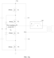
- FIG. 10a is an example schematic of another specific circuit structure of a half-bridge circuit in a power conversion apparatus according to this application.
- the upper bridge arm switch Q1 and the lower bridge arm switch Q2 in the half-bridge circuit may each be implemented by using two switching transistors, and form a three-level LLC circuit.
- the upper bridge arm switch Q1 may include a first switching transistor T1 and a second switching transistor T2 that are connected in series
- the lower bridge arm switch Q2 may include a third switching transistor T3 and a fourth switching transistor T4 that are connected in series.
- the second switching transistor T2 is coupled between the first switching transistor T1 and the first connection point P1
- the third switching transistor T3 is coupled between the fourth switching transistor T4 and the first connection point P1.
- the logic circuit 230 may output a first enable signal to the drive circuit 240 based on a received first drive signal output by the chip, where the first enable signal is a necessary condition for turning on the first switching transistor T1; and output a second enable signal to the drive circuit 240 based on a received second drive signal output by the chip, where the second enable signal is a necessary condition for turning on the second switching transistor T2.
- the logic circuit 230 may output a third enable signal to the drive circuit 240 based on a received third drive signal output by the chip, where the third enable signal is a necessary condition for turning on the third switching transistor T3; and the WIR outputs a fourth enable signal to the drive circuit 240 based on a received fourth drive signal output by the chip, where the fourth enable signal is a necessary condition for turning on the fourth switching transistor T4.
- the drive circuit 240 may generate a first PWM signal PWM1 and output the first PWM signal to the first switching transistor T1.
- the drive circuit 240 may generate a second PWM signal 3 and output the second PWM signal to the third switching transistor T3. After receiving the fourth enable signal, the drive circuit 240 may generate a fourth PWM signal PWM4 and output the fourth PWM signal to the fourth switching transistor T4.
- FIG. 10b is an example schematic of another specific circuit structure of a drive circuit in a power conversion apparatus according to this application.
- the logic circuit 230 may specifically include a first comparison circuit 231, a second comparison circuit 232, a first AND logic circuit 235, a second AND logic circuit 236, a third AND logic circuit 237, and a fourth AND logic circuit 238.
- the first comparison circuit 231 outputs a first high level signal H1 when it is determined that the voltage Va of the first connection point P1 is greater than the first threshold V1.
- the second comparison circuit 232 outputs a second high level signal H2 when it is determined that the voltage Va of the first connection point P1 is less than the second threshold V2.
- the first AND logic circuit 235 may perform AND logic with the first drive signal output by the chip, to generate and output the first enable signal, so that the drive circuit 240 may generate the first PWM signal PWM1 after receiving the first enable signal, to drive the first switching transistor T1.
- the second AND logic circuit 236 may perform AND logic with the second drive signal output by the chip, to generate and output the second enable signal, so that the drive circuit 240 may generate the second PWM signal PWM2 after receiving the second enable signal, to drive the second switching transistor T2.
- the third AND logic circuit 237 may perform AND logic with the third drive signal output by the chip, to generate and output the third enable signal, so that the drive circuit 240 may generate the third PWM signal PWM3 after receiving the third enable signal, to drive the third switching transistor T3.
- the fourth AND logic circuit 238 may perform AND logic with the fourth drive signal output by the chip, to generate and output the fourth enable signal, so that the drive circuit 240 may generate the fourth PWM signal PWM4 after receiving the fourth enable signal, to drive the fourth switching transistor T4.
- FIG. 11 is an example schematic of other specific circuit control of a three-level LLC circuit in a power conversion apparatus according to this application.
- the three-level LLC circuit may include a first bridge arm TA and a second bridge arm TB that are connected in series.
- the first bridge arm TA may include an upper bridge arm switch Q1 and a lower bridge arm switch Q2 that are connected in series.
- a first connection point P1 between the upper bridge arm switch Q1 and the lower bridge arm switch Q2 may be referred to as a midpoint of the first bridge arm TA.
- the second bridge arm TB may include an upper bridge arm switch Q3 and a lower bridge arm switch Q4 that are connected in series.
- a second connection point P2 between the upper bridge arm switch Q3 and the lower bridge arm switch Q4 may be referred to as a midpoint of the second bridge arm TB.
- the upper bridge arm switch Q1 of the first bridge arm TA is connected to an input voltage terminal Vin
- the lower bridge arm switch Q4 of the second bridge arm TB is grounded
- the lower bridge arm switch Q2 of the first bridge arm TA is connected to the upper bridge arm switch Q3 of the second bridge arm TB.
- a positive terminal BAT+ of the battery may be used as an input voltage terminal Vin
- a negative terminal BAT- of the battery may be grounded
- a first terminal of a secondary-side winding Sr is coupled to the midpoint of the first bridge arm TA, namely, the first connection point P1
- a second terminal of the secondary-side winding Sr is coupled to the midpoint of the second bridge arm TB, namely, the second connection point P2.
- a high-voltage positive input terminal HV+ may be used as an input voltage terminal Vin
- a high-voltage negative input terminal HV- may be grounded
- a first terminal of a primary-side winding Pr is coupled to the midpoint of the first bridge arm TA, namely, the first connection point P1
- a second terminal of the primary-side winding Pr is coupled to the midpoint of the second bridge arm TB, namely, the second connection point P2.
- a resonance circuit 103 may be further disposed between the full-bridge circuit and the primary-side winding (or the secondary-side winding).
- the resonance circuit 103 may be coupled between a first end of the primary-side winding (or the secondary-side winding) and a first connection point P1, or the resonance circuit 103 may be coupled between a second end of the primary-side winding (or the secondary-side winding) and a second connection point P2.
- the resonance circuit 103 may include an inductor L, and the resonance circuit 103 may further include a capacitor C connected in series to the inductor L.
- the controller 200 may be coupled to the first bridge arm TA and the second bridge arm TB of the three-level LLC circuit.
- the controller 200 controls working modes of the upper bridge arm switch Q1 and the lower bridge arm switch Q2 of the first bridge arm TA based on a voltage of the first connection point P1 between the upper bridge arm switch Q1 and the lower bridge arm switch Q2 in the first bridge arm TA.
- the controller 200 controls turn-on/off of the upper bridge arm switch Q3 and the lower bridge arm switch Q4 of the second bridge arm TB based on a voltage of the second connection point P2 between the upper bridge arm switch Q3 and the lower bridge arm switch Q4 in the second bridge arm TB.
- the controller 200 may sample the voltages of the first connection point P1 and the second connection point P2. When it is determined that the voltage of the first connection point P1 is greater than the first threshold V1, the controller determines that the lower bridge arm switch Q2 of the first bridge arm TA is not short-circuited, and may control, based on a PWM drive signal sent by the control chip, the upper bridge arm switch Q1 of the first bridge arm TA to switch between being turned on and being turned off. To be specific, at a moment, the upper bridge arm switch Q1 of the first bridge arm TA is controlled to be turned on, and at a next moment, the upper bridge arm switch Q1 of the first bridge arm TA is controlled to be turned off.
- the controller determines that the upper bridge arm switch Q1 of the first bridge arm TA is not short-circuited, and may control, based on a PWM drive signal sent by the control chip, the lower bridge arm switch Q2 of the first bridge arm TA to switch between being turned on and being turned off.
- the lower bridge arm switch Q2 of the first bridge arm TA is controlled to be turned on, and at a next moment, the lower bridge arm switch Q2 of the first bridge arm TA is controlled to be turned off.
- the controller determines that the lower bridge arm switch Q4 of the second bridge arm TB is not short-circuited, and may control, based on a PWM drive signal sent by the control chip, the upper bridge arm switch Q3 of the second bridge arm TB to switch between being turned on and being turned off.
- the upper bridge arm switch Q3 of the second bridge arm TB is controlled to be turned on, and at a next moment, the upper bridge arm switch Q3 of the second bridge arm TB is controlled to be turned off.
- the controller determines that the upper bridge arm switch Q3 of the second bridge arm TB is not short-circuited, and may control, based on a PWM drive signal sent by the control chip, the lower bridge arm switch Q4 of the second bridge arm TB to switch between being turned on and being turned off.
- the lower bridge arm switch Q4 of the second bridge arm TB is controlled to be turned on, and at a next moment, the lower bridge arm switch Q4 of the second bridge arm TB is controlled to be turned off.
- the controller determines that the lower bridge arm switch Q2 of the first bridge arm TA is short-circuited, and may control the upper bridge arm switch Q1 of the first bridge arm TA to be turned off, to avoid a possibility that bridge arm straight-through occurs.
- the controller determines that the upper bridge arm switch Q1 of the first bridge arm TA is short-circuited, and may control the lower bridge arm switch Q2 of the first bridge arm TA to be turned off, to avoid a possibility that bridge arm straight-through occurs.
- the controller determines that the lower bridge arm switch Q4 of the second bridge arm TB is short-circuited, and may control the upper bridge arm switch Q3 of the second bridge arm TB to be turned off, to avoid a possibility that bridge arm straight-through occurs.
- the controller determines that the upper bridge arm switch Q3 of the second bridge arm TB is short-circuited, and may control the lower bridge arm switch Q4 of the second bridge arm TB to be turned off, to avoid a possibility that bridge arm straight-through occurs.
- the first threshold V1, the second threshold V2, the third threshold V3, and the fourth threshold V4 may each be between 0 and Vin, in other words, 0 ⁇ V1 ⁇ Vin, 0 ⁇ V2 ⁇ Vin, 0 ⁇ V3 ⁇ Vin, and 0 ⁇ V4 ⁇ Vin.
- the controller 200 may include a first sampling circuit 210, a second sampling circuit 220, a logic circuit 230, and a drive circuit 240.
- the first sampling circuit 210 may sample the voltage of the first connection point P1 and output the voltage to the logic circuit 230
- the second sampling circuit 220 may sample the voltage of the second connection point P2 and output the voltage to the logic circuit 230.
- the logic circuit 230 may output a first enable signal to the drive circuit 240 based on a received first drive signal output by the chip, where the first enable signal is a necessary condition for turning on the upper bridge arm switch Q1 of the first bridge arm TA.
- the logic circuit 230 may output a second enable signal to the drive circuit 240 based on a received second drive signal output by the chip, where the second enable signal is a necessary condition for turning on the lower bridge arm switch Q2 of the first bridge arm TA.
- the logic circuit 230 may output a third enable signal to the drive circuit 240 based on a received third drive signal output by the chip, where the third enable signal is a necessary condition for turning on the upper bridge arm switch Q3 of the second bridge arm TB.
- the logic circuit 230 may output a fourth enable signal to the drive circuit 240 based on a received fourth drive signal output by the chip, where the fourth enable signal is a necessary condition for turning on the lower bridge arm switch Q4 of the second bridge arm TB.
- the drive circuit 240 may generate a first PWM signal PWM1 and output the first PWM signal to the upper bridge arm switch Q1 of the first bridge arm TA.
- the drive circuit 240 may generate a second PWM signal PWM2 and output the second PWM signal to the lower bridge arm switch Q2 of the first bridge arm TA.
- the drive circuit 240 may generate a third PWM signal PWM3 and output the third PWM signal to the upper bridge arm switch Q3 of the second bridge arm TB.
- the drive circuit 240 may generate a fourth PWM signal PWM4 and output the fourth PWM signal to the lower bridge arm switch Q4 of the second bridge arm TB.
- FIG. 12 is an example schematic of another specific circuit structure of a drive circuit in a power conversion apparatus according to this application.
- the logic circuit 230 may specifically include a first comparison circuit 231, a second comparison circuit 232, a third comparison circuit 233, a fourth comparison circuit 234, a first AND logic circuit 235, a second AND logic circuit 236, a third AND logic circuit 237, and a fourth AND logic circuit 238.
- the first comparison circuit 231 outputs a first high level signal H1 when it is determined that the voltage Va of the first connection point P1 is greater than the first threshold V1.
- the second comparison circuit 232 outputs a second high level signal H2 when it is determined that the voltage Va of the first connection point P1 is less than the second threshold V2.
- the third comparison circuit 233 outputs a third high level signal H3 when it is determined that the voltage Vb of the second connection point P2 is greater than the third threshold V3.
- the fourth comparison circuit 234 outputs a fourth high level signal H4 when it is determined that the voltage Vb of the second connection point P2 is less than the fourth threshold V4.
- the first AND logic circuit 235 may perform AND logic with the first drive signal output by the chip, to generate and output the first enable signal, so that the drive circuit 240 may generate the first PWM signal PWM1 after receiving the first enable signal, to drive the upper bridge arm switch Q1 of the first bridge arm TA.
- the second AND logic circuit 236 may perform AND logic with the second drive signal output by the chip, to generate and output the second enable signal, so that the drive circuit 240 may generate the second PWM signal PWM2 after receiving the second enable signal, to drive the lower bridge arm switch Q2 of the first bridge arm TA.
- the third AND logic circuit 237 may perform AND logic with the third drive signal output by the chip, to generate and output the third enable signal, so that the drive circuit 240 may generate the third PWM signal PWM3 after receiving the third enable signal, to drive the upper bridge arm switch Q3 of the second bridge arm TB.
- the fourth AND logic circuit 238 may perform AND logic with the fourth drive signal output by the chip, to generate and output the fourth enable signal, so that the drive circuit 240 may generate the fourth PWM signal PWM4 after receiving the fourth enable signal, to drive the lower bridge arm switch Q4 of the second bridge arm TB.
- AND logic circuit mentioned in the foregoing several embodiments is a specific implementation of an enable output circuit, and the AND logic circuit may also be replaced with another enable output circuit.
- an embodiment of this application further provides an energy storage apparatus.
- the energy storage apparatus may include a BCU, a plurality of battery packs (the battery pack may be considered as the foregoing battery 300), and a plurality of power conversion apparatuses provided in the embodiments of this application.
- the plurality of battery packs are disposed in parallel, and each of the battery packs is connected to the BCU after being connected in series to one power conversion apparatus.
- the battery may be coupled to a secondary-side circuit in the power conversion apparatus.
- the controller in the power conversion apparatus may collect a voltage of a connection point between an upper bridge arm switch and a lower bridge arm switch in a bridge arm of the secondary-side circuit, and control working modes of the upper bridge arm switch and the lower bridge arm switch in the corresponding bridge arm based on the voltage of the connection point, to reduce a possibility that bridge arm straight-through occurs, and prevent a battery pack short-circuit.
Landscapes
- Engineering & Computer Science (AREA)
- Power Engineering (AREA)
- Inverter Devices (AREA)
- Microelectronics & Electronic Packaging (AREA)
- Manufacturing & Machinery (AREA)
- Chemical & Material Sciences (AREA)
- Chemical Kinetics & Catalysis (AREA)
- Electrochemistry (AREA)
- General Chemical & Material Sciences (AREA)
- Dc-Dc Converters (AREA)
Abstract
This application provides a power conversion apparatus and an energy storage apparatus. The power conversion apparatus may include a direct current-direct current conversion circuit and a controller. The direct current-direct current conversion circuit may include a full-bridge circuit, the full-bridge circuit includes a first bridge arm and a second bridge arm that are connected in parallel, and each of the bridge arms includes an upper bridge arm switch and a lower bridge arm switch that are connected in series. The controller is coupled to each of the bridge arms, and the controller controls turn-on/off of the upper bridge arm switch and the lower bridge arm switch of each of the bridge arms based on a voltage of a first connection point between the upper bridge arm switch and the lower bridge arm switch in the first bridge arm and a voltage of a second connection point between the upper bridge arm switch and the lower bridge arm switch in the second bridge arm, to reduce a possibility that bridge arm straight-through occurs.
Description
- This application relates to the field of electronic technologies, and in particular, to a power conversion apparatus and an energy storage apparatus.
- A lithium battery has features such as high energy density and long cycle life, and therefore is widely used in the field of photovoltaic energy storage and electric vehicles. A battery needs to perform energy conversion by using a power conversion circuit. A circuit topology formed by a bridge arm, such as a half-bridge circuit and a full-bridge circuit, is widely used in the power conversion circuit. If straight-through occurs on an upper transistor and a lower transistor that form the bridge arm, the entire bridge arm is short-circuited, and a large current is generated. This causes damage or even explosion of switching transistors. Currently, there are two main manners of preventing bridge arm straight-through: (1) A current of a switching transistor is detected, and an operation of stopping sending a PWM driver gating signal is driven after the current overflows. (2) Logical interlocking is performed on drive signals of an upper transistor and a lower transistor. A short-circuit current flows through the switching transistor for a specific period of time in a manner of detecting the short-circuit current of the switching transistor. In this case, the operation of stopping sending a PWM driver gating signal may not be performed in time, and the switching transistor may still be damaged.
- This application provides a power conversion apparatus and an energy storage apparatus, to avoid a bridge arm straight-through problem.
- According to a first aspect, an embodiment of this application provides a power conversion apparatus. The power conversion apparatus includes a direct current-direct current conversion circuit and a controller. The direct current-direct current conversion circuit includes a full-bridge circuit, the full-bridge circuit includes a first bridge arm and a second bridge arm that are connected in parallel, and each of the bridge arms includes an upper bridge arm switch and a lower bridge arm switch that are connected in series. The controller is coupled to each of the bridge arms. The controller may control turn-on/off of the upper bridge arm switch and the lower bridge arm switch of each of the bridge arms based on a voltage of a first connection point between the upper bridge arm switch and the lower bridge arm switch in the first bridge arm and a voltage of a second connection point between the upper bridge arm switch and the lower bridge arm switch in the second bridge arm. For example, when it is determined that the voltage of the first connection point and the voltage of the second connection point meet a specified control requirement, it indicates that a short-circuit problem does not occur on some bridge arm switches, and corresponding bridge arm switches may be driven according to a PWM drive signal sent by a control chip. To be specific, the corresponding bridge arm switches are controlled to switch between being turned on and being turned off. When it is determined that the voltage of the first connection point or the voltage of the second connection point does not meet the specified control requirement, it indicates that a short-circuit problem is very likely to occur in a bridge arm switch, and the corresponding bridge arm switch needs to be turned off. To be specific, the corresponding bridge arm switch is controlled to be turned off, to reduce a possibility that bridge arm straight-through occurs.
- In some embodiments, when it is determined that at least one of following is met: the voltage of the first connection point is less than the first threshold and the voltage of the second connection point is greater than the second threshold, the controller determines that at least one of the lower bridge arm switch of the first bridge arm and the upper bridge arm switch of the second bridge arm is short-circuited, and controls both the upper bridge arm switch of the first bridge arm and the lower bridge arm switch of the second bridge arm to be turned off, to avoid a possibility that bridge arm straight-through occurs.
- In some embodiments, when it is determined that the voltage of the first connection point is greater than the first threshold and the voltage of the second connection point is less than the second threshold, the controller determines that the lower bridge arm switch of the first bridge arm and the upper bridge arm switch of the second bridge arm are not short-circuited, and controls, based on a PWM drive signal sent by the control chip, the upper bridge arm switch of the first bridge arm and the lower bridge arm switch of the second bridge arm to be simultaneously turned on or turned off. To be specific, at a moment, the upper bridge arm switch of the first bridge arm and the lower bridge arm switch of the second bridge arm are controlled to be simultaneously turned on, and at a next moment, the upper bridge arm switch of the first bridge arm and the lower bridge arm switch of the second bridge arm are controlled to be simultaneously turned off.
- In some embodiments, when it is determined that at least one of following is met: the voltage of the second connection point is less than the first threshold and the voltage of the first connection point is greater than the second threshold, the controller determines that at least one of the upper bridge arm switch of the first bridge arm and the lower bridge arm switch of the second bridge arm is short-circuited, and controls both the upper bridge arm switch of the second bridge arm and the lower bridge arm switch of the first bridge arm to be turned off, to avoid a possibility that bridge arm straight-through occurs.
- In some embodiments, when it is determined that the voltage of the second connection point is greater than the first threshold and the voltage of the first connection point is less than the second threshold, the controller determines that the upper bridge arm switch of the first bridge arm and the lower bridge arm switch of the second bridge arm are not short-circuited, and controls, based on a PWM drive signal sent by the control chip, the upper bridge arm switch of the second bridge arm and the lower bridge arm switch of the first bridge arm to be simultaneously turned on or turned off. To be specific, at a moment, the upper bridge arm switch of the second bridge arm and the lower bridge arm switch of the first bridge arm are controlled to be simultaneously turned on, and at a next moment, the upper bridge arm switch of the second bridge arm and the lower bridge arm switch of the first bridge arm are controlled to be simultaneously turned off.
- According to a second aspect, an embodiment of this application provides another power conversion apparatus. The power conversion apparatus includes a direct current-direct current conversion circuit and a controller. The direct current-direct current conversion circuit includes a half-bridge circuit, the half-bridge circuit includes a first bridge arm, and the first bridge arm includes an upper bridge arm switch and a lower bridge arm switch that are connected in series. The controller is coupled to the first bridge arm. The controller may control turn-on/off of the upper bridge arm switch and the lower bridge arm switch of the first bridge arm based on a voltage of a first connection point between the upper bridge arm switch and the lower bridge arm switch in the first bridge arm. For example, when it is determined that the voltage of the first connection point meets a specified control requirement, it indicates that a short-circuit problem does not occur on some bridge arm switches, and corresponding bridge arm switches may be driven according to a PWM drive signal sent by a control chip. To be specific, the corresponding bridge arm switches are controlled to be turned on or turned off. When it is determined that the voltage of the first connection point does not meet the specified control requirement, it indicates that a short-circuit problem is very likely to occur in a bridge arm switch, and the corresponding bridge arm switch needs to be turned off. To be specific, the corresponding bridge arm switch is controlled to be turned off, to reduce a possibility that bridge arm straight-through occurs.
- In some embodiments, when it is determined that the voltage of the first connection point is less than a first threshold, the controller determines that the lower bridge arm switch of the first bridge arm is short-circuited, and controls the upper bridge arm switch to be turned off, to avoid a possibility that bridge arm straight-through occurs.
- In some embodiments, when it is determined that the voltage of the first connection point is greater than the first threshold, the controller determines that the lower bridge arm switch of the first bridge arm is not short-circuited, and controls, based on a PWM drive signal sent by the control chip, the upper bridge arm switch to switch between being turned on and being turned off. To be specific, at a moment, the upper bridge arm switch is controlled to be turned on, and at a next moment, the upper bridge arm switch is controlled to be turned off.
- In some embodiments, when it is determined that the voltage of the first connection point is greater than a second threshold, the controller determines that the lower bridge arm switch of the first bridge arm is short-circuited, and controls the lower bridge arm switch to be turned off, to avoid a possibility that bridge arm straight-through occurs.
- In some embodiments, when it is determined that the voltage of the first connection point is less than the second threshold, the controller determines that the lower bridge arm switch of the first bridge arm is not short-circuited, and controls, based on a PWM drive signal sent by the control chip, the lower bridge arm switch to switch between being turned on and being turned off. To be specific, at a moment, the lower bridge arm switch is controlled to be turned on, and at a next moment, the lower bridge arm switch is controlled to be turned off.
- According to a third aspect, an embodiment of this application provides another power conversion apparatus. The power conversion apparatus includes a direct current-direct current conversion circuit and a controller. The direct current-direct current conversion circuit includes an LLC circuit, the LLC circuit includes a first bridge arm and a second bridge arm that are connected in series, and each of the bridge arms includes an upper bridge arm switch and a lower bridge arm switch that are connected in series. The controller is coupled to each of the bridge arms. The controller may control turn-on/off of the upper bridge arm switch and the lower bridge arm switch of the first bridge arm based on a voltage of a first connection point between the upper bridge arm switch and the lower bridge arm switch in the first bridge arm. The controller may control turn-on/off of the upper bridge arm switch and the lower bridge arm switch of the second bridge arm based on a voltage of a second connection point between the upper bridge arm switch and the lower bridge arm switch in the second bridge arm. For example, when it is determined that the voltage of the first connection point or the voltage of the second connection point meets a specified control requirement, it indicates that a short-circuit problem does not occur on some bridge arm switches, and corresponding bridge arm switches may be driven according to a PWM drive signal sent by a control chip. To be specific, the corresponding bridge arm switches are controlled to switch between being turned on and being turned off. When it is determined that the voltage of the first connection point or the voltage of the second connection point does not meet the specified control requirement, it indicates that a short-circuit problem is very likely to occur in a bridge arm switch, and the corresponding bridge arm switch needs to be turned off. To be specific, the corresponding bridge arm switch is controlled to be turned off, to reduce a possibility that bridge arm straight-through occurs.
- In some embodiments, when it is determined that the voltage of the first connection point is less than a first threshold, the controller determines that the lower bridge arm switch of the first bridge arm is short-circuited, and controls the upper bridge arm switch of the first bridge arm to be turned off, to avoid a possibility that bridge arm straight-through occurs.
- In some embodiments, when it is determined that the voltage of the first connection point is greater than the first threshold, the controller determines that the lower bridge arm switch of the first bridge arm is not short-circuited, and controls, based on a PWM drive signal sent by the control chip, the upper bridge arm switch of the first bridge arm to switch between being turned on and being turned off. To be specific, at a moment, the upper bridge arm switch of the first bridge arm is controlled to be turned on, and at a next moment, the upper bridge arm switch of the first bridge arm is controlled to be turned off.
- In some embodiments, when it is determined that the voltage of the first connection point is greater than a second threshold, the controller determines that the upper bridge arm switch of the first bridge arm is short-circuited, and controls the lower bridge arm switch of the first bridge arm to be turned off, to avoid a possibility that bridge arm straight-through occurs.
- In some embodiments, when it is determined that the voltage of the first connection point is less than the second threshold, the controller determines that the upper bridge arm switch of the first bridge arm is not short-circuited, and controls, based on a PWM drive signal sent by the control chip, the lower bridge arm switch of the first bridge arm to switch between being turned on and being turned off. To be specific, at a moment, the lower bridge arm switch of the first bridge arm is controlled to be turned on, and at a next moment, the lower bridge arm switch of the first bridge arm is controlled to be turned off.
- In some embodiments, when it is determined that the voltage of the second connection point is less than a third threshold, the controller determines that the lower bridge arm switch of the second bridge arm is short-circuited, and controls the upper bridge arm switch of the second bridge arm to be turned off, to avoid a possibility that bridge arm straight-through occurs.
- In some embodiments, when it is determined that the voltage of the second connection point is greater than the third threshold, the controller determines that the lower bridge arm switch of the second bridge arm is not short-circuited, and controls, based on a PWM drive signal sent by the control chip, the upper bridge arm switch of the second bridge arm to switch between being turned on and being turned off. To be specific, at a moment, the upper bridge arm switch of the second bridge arm is controlled to be turned on, and at a next moment, the upper bridge arm switch of the second bridge arm is controlled to be turned off.
- In some embodiments, when it is determined that the voltage of the second connection point is greater than a fourth threshold, the controller determines that the upper bridge arm switch of the second bridge arm is short-circuited, and controls the lower bridge arm switch of the second bridge arm to be turned off, to avoid a possibility that bridge arm straight-through occurs.
- In some embodiments, when it is determined that the voltage of the second connection point is less than the fourth threshold, the controller determines that the upper bridge arm switch of the second bridge arm is not short-circuited, and controls, based on a PWM drive signal sent by the control chip, the lower bridge arm switch of the second bridge arm to switch between being turned on and being turned off. To be specific, at a moment, the lower bridge arm switch of the second bridge arm is controlled to be turned on, and at a next moment, the lower bridge arm switch of the second bridge arm is controlled to be turned off.
- According to a fourth aspect, an embodiment of this application further provides an energy storage apparatus, including a battery control unit, a plurality of battery packs, and a plurality of power conversion apparatuses according to any one of the first aspect to the third aspect. The plurality of battery packs are disposed in parallel, and each of the battery packs is connected to the battery control unit after being connected in series to one power conversion apparatus. The power conversion apparatus includes a primary-side circuit, a primary-side winding, a secondary-side winding, and a secondary-side circuit that are sequentially coupled. The secondary-side circuit is coupled to the battery pack. The secondary-side circuit may be a full-bridge circuit, a half-bridge circuit, or an LLC circuit. The controller in the power conversion apparatus may collect a voltage of a connection point between an upper bridge arm switch and a lower bridge arm switch in a bridge arm of the secondary-side circuit, and control turn-on/off of the upper bridge arm switch and the lower bridge arm switch in the corresponding bridge arm based on the voltage of the connection point, to reduce a possibility that bridge arm straight-through occurs, and prevent a battery pack short-circuit.
-
-
FIG. 1 is a schematic of a frame structure of a photovoltaic system; -
FIG. 2 is a schematic of a structure of an energy storage apparatus; -
FIG. 3 is a schematic of a structure of a power conversion apparatus; -
FIG. 4 is a schematic of a specific circuit structure of a power conversion apparatus according to this application; -
FIG. 5 is a schematic of specific circuit control of a full-bridge circuit in a power conversion apparatus according to this application; -
FIG. 6 is a schematic of a specific circuit structure of a drive circuit in a power conversion apparatus according to this application; -
FIG. 7a is a schematic of a specific circuit structure of a full-bridge circuit in a power conversion apparatus according to this application; -
FIG. 7b is a schematic of another specific circuit structure of a full-bridge circuit in a power conversion apparatus according to this application; -
FIG. 7c is a schematic of another specific circuit structure of a full-bridge circuit in a power conversion apparatus according to this application; -
FIG. 8 is a schematic of specific circuit control of a half-bridge circuit in a power conversion apparatus according to this application; -
FIG. 9a is a schematic of a specific circuit structure of a half-bridge circuit in a power conversion apparatus according to this application; -
FIG. 9b is a schematic of another specific circuit structure of a drive circuit in a power conversion apparatus according to this application; -
FIG. 10a is a schematic of another specific circuit structure of a half-bridge circuit in a power conversion apparatus according to this application; -
FIG. 10b is a schematic of another specific circuit structure of a drive circuit in a power conversion apparatus according to this application; -
FIG. 11 is a schematic of other specific circuit control of a three-level LLC circuit in a power conversion apparatus according to this application; and -
FIG. 12 is a schematic of another specific circuit structure of a drive circuit in a power conversion apparatus according to this application. - 110: photovoltaic array; 120: power converter; 130: power grid; 140: external load; 150: energy storage apparatus; 100: DC-DC conversion circuit; 200: controller; 300: battery; 101: primary-side circuit; Pr: primary-side winding; Sr: secondary-side winding; 102: secondary-side circuit; 103: resonance circuit; 210: first sampling circuit; 220: second sampling circuit; 230: logic circuit; 240: drive circuit; 231: first comparison circuit; 232: second comparison circuit; 233: third comparison circuit; 234: fourth comparison circuit; 235: first AND logic circuit; 236: second AND logic circuit; 237: third AND logic circuit; 238: fourth AND logic circuit; P1: first connection point; P2: second connection point; TA: first bridge arm; TB: second bridge arm; TC: capacitor branch; Q1 and Q3: upper bridge arm switches; Q2 and Q4: lower bridge arm switches; T1: first switching transistor; T2: second switching transistor; T3: third switching transistor; T4: fourth switching transistor; L: inductor; C: capacitor; C1: first capacitor; C2: second capacitor.
- To make objectives, technical solutions, and advantages of this application clearer, the following further describes this application in detail with reference to accompanying drawings. A specific operation method in a method embodiment may also be applied to an apparatus embodiment or a system embodiment. It should be noted that, in the description of this application, "at least one" means one or more, and "a plurality of" means two or more. In view of this, in embodiments of the present invention, "a plurality of" may also be understood as "at least two". The term "and/or" is an association relationship for describing associated objects and represents that three relationships may exist. For example, A and/or B may represent the following three cases: Only A exists, both A and B exist, and only B exists. In addition, the character "/" generally indicates an "or" relationship between the associated objects. In addition, it should be understood that, in the description of this application, terms "first" and "second" are only used to distinguish the purpose of the description, but cannot be understood as indication or implication of relative importance, and cannot be understood as an indication or implication of a sequence.
- It should be noted that the "connection" in embodiments of this application may be understood as an electric connection, and a connection between two electrical elements may be a direct or indirect connection between the two electrical elements. For example, a connection between A and B may be a direct connection between A and B, or may be an indirect connection between A and B through one or more other electrical elements. For example, that A is connected to B may also be that A is directly connected to C, C is directly connected to B, A and B are connected through C. In some scenarios, the "connection" may also be understood as coupling, for example, electromagnetic coupling between two inductors. In conclusion, the connection between A and B enables transmission of electric energy between A and B.
- The following clearly the technical solutions in embodiments of this application with reference to accompanying drawings in embodiments of this application. First, an application scenario of a power conversion apparatus provided in embodiments of this application is described. The power conversion apparatus provided in embodiments of this application may be used in a scenario such as a photovoltaic system or an energy storage apparatus.
-
FIG. 1 is an example of a schematic of a frame structure of a photovoltaic system. Refer toFIG. 1 . The photovoltaic system includes aphotovoltaic array 110, apower converter 120, anenergy storage apparatus 150, and apower grid 130 or anexternal load 140. Thepower converter 120 may integrate a DC/DC conversion circuit and a DC/AC conversion circuit. Theenergy storage apparatus 150 may be located between the DC/DC conversion circuit and the DC/AC conversion circuit. After the DC/DC conversion circuit performs boost or buck conversion on electric energy generated by thephotovoltaic array 110, electric energy obtained after the conversion may be used to charge theenergy storage apparatus 150. When the electric energy generated by thephotovoltaic array 110 is insufficient to supply power to thepower grid 130 or theexternal load 140, electric energy stored in theenergy storage apparatus 150 may be transmitted to thepower grid 130 or theexternal load 140 through the DC/AC conversion circuit in thepower converter 120. In addition, theenergy storage apparatus 150 may further receive power supply from thepower grid 130, and an alternating current output by thepower grid 130 is converted into a direct current by using the DC/AC conversion circuit, and then is transmitted to theenergy storage apparatus 150, so as to charge theenergy storage apparatus 150. -
FIG. 2 is an example schematic of a structure of an energy storage apparatus. Refer toFIG. 2 . Theenergy storage apparatus 150 may include a battery control unit (battery control unit, BCU), a plurality of battery packs, and a plurality of power conversion apparatuses. The power conversion apparatus includes a direct current (direct current, DC)-direct current conversion circuit (also referred to as a DC/DC conversion circuit or a DC-DC conversion circuit for short). The plurality of battery packs are disposed in parallel, and each of the battery pack is connected to the battery control unit after being connected to a DC-DC conversion circuit in series. The DC-DC conversion circuit may perform power conversion on electric energy stored in the battery pack and then output electric energy obtained after the conversion, or perform power conversion on external power supply and then store, in the battery pack, external power supply obtained after the conversion. -
FIG. 3 is an example schematic of a structure of a power conversion apparatus. Refer toFIG. 3 . In addition to the DC-DC conversion circuit 100, the power conversion apparatus may further include acontroller 200. The DC-DC conversion circuit 100 may include a primary-side circuit 101, a secondary-side circuit 102, and a transformer. The transformer usually includes a primary-side winding Pr and a secondary-side winding Sr. The primary-side circuit 101, the primary-side winding Pr, the secondary-side winding Sr, and the secondary-side circuit 102 may be sequentially coupled. Optionally, a battery 300 (which may also be referred to as a battery pack) is usually coupled to the secondary-side circuit 102. Alternatively, thebattery 300 may be coupled to the primary-side circuit 101. An example in which thebattery 300 is coupled to the secondary-side circuit 102 is used for description below. - The
controller 200 is connected to the primary-side circuit 101 and the secondary-side circuit 102. Thecontroller 200 may generate a plurality of control signals, for example, a pulse width modulation (pulse width modulation, PWM) signal, to control the primary-side circuit 101 and the secondary-side circuit 102 to work. For example, thecontroller 200 may be any one of a microprocessor (microcontroller unit, MCU), a general-purpose central processing unit (central processing unit, CPU), a general-purpose processor, digital signal processing (digital signal processing, DSP), an application-specific integrated circuit (application-specific integrated circuit, ASIC), a field programmable gate array (field programmable gate array, FPGA), or the like inside the conversion circuit, or may be any one or a combination of another programmable logic device, a transistor logic device, or a hardware component. During specific implementation, a plurality of power conversion apparatuses may share asame controller 200, or may be separately provided withdifferent controllers 200. In addition, thecontroller 200 may be independently disposed, or may be integrated into another component, for example, may be integrated into a BCU. - In some application scenarios, the
controller 200 may control the DC-DC conversion circuit 100 to convert high-voltage direct-current electric energy into low-voltage direct-current electric energy, and output the low-voltage direct-current electric energy to thebattery 300, to charge thebattery 300. In the DC-DC conversion circuit 100, the primary-side circuit 101 may receive high-voltage direct-current electric energy, and the secondary-side circuit 102 may output low-voltage direct-current electric energy. Therefore, the primary-side circuit 101 may also be generally referred to as a high-voltage side circuit, and the secondary-side circuit 102 may also be generally referred to as a low-voltage side circuit. In some other application scenarios, in the power conversion apparatus provided in this embodiment of this application, thecontroller 200 may control the DC-DC conversion circuit 100 to perform voltage conversion on direct-current electric energy stored in thebattery 300, and then output electric energy obtained after the conversion, to discharge thebattery 300. -
FIG. 4 is an example schematic of a specific circuit structure of a power conversion apparatus according to this application. Refer toFIG. 4 . Aprimary-side circuit 101 and a secondary-side circuit 102 in the power conversion apparatus may be implemented by using a full-bridge circuit topology, a half-bridge circuit topology, an LLC circuit topology, or another circuit topology. InFIG. 4 , an example in which the primary-side circuit 101 is a half-bridge circuit topology and the secondary-side circuit 102 is a full-bridge circuit topology is used for description. A full-bridge circuit topology and a half-bridge circuit topology may each include a bridge arm formed by a plurality of switches or switching transistors connected in series. Specifically, one bridge arm may include an upper bridge arm switch and a lower bridge arm switch that are connected in series. The full-bridge circuit topology includes two bridge arms connected in parallel, and the half-bridge circuit topology includes one bridge arm and a capacitor connected in parallel. The upper bridge arm switch is usually located at an upper end of the bridge arm and is connected to a high-potential voltage terminal, and the lower bridge arm switch is usually located at a lower end of the bridge arm and is connected to a low-potential voltage terminal. A voltage value of the high-potential voltage terminal is higher than a voltage value of the low-potential voltage terminal. For example, the high-potential voltage terminal may be an input voltage terminal Vin, and the low-potential voltage terminal may be a ground voltage. In addition, in the secondary-side circuit 102, a high-potential voltage terminal connected to an upper bridge arm switch may be a positive terminal BAT+ of abattery 300, and a low-potential voltage terminal connected to a lower bridge arm switch may be a negative terminal BAT- of thebattery 300. In the primary-side circuit 101, a high-potential voltage terminal connected to an upper bridge arm switch may be a high-voltage positive input terminal HV+, and a low-potential voltage terminal connected to a lower bridge arm switch may be a high-voltage negative input terminal HV-. - In this embodiment of this application, switches or switching transistors in the primary-
side circuit 101 and the secondary-side circuit 102 may be one or more of a plurality of types of switches such as a relay, a metal-oxide semiconductor field-effect transistor (metal-oxide semiconductor field-effect transistor, MOSFET), a bipolar junction transistor (bipolar junction transistor, BJT), and an insulated gate bipolar transistor (insulated gate bipolar transistor, IGBT). Details are not listed in this embodiment of this application. A switching transistor may include a first electrode, a second electrode, and a control electrode, and the control electrode is configured to control turn-on/off of the switching transistor. When the switching transistor is turned on, a current can be transmitted between the first electrode and the second electrode of the switching transistor. When the switching transistor is turned off, no current can be transmitted between the first electrode and the second electrode of the switching transistor. The MOSFET is used as an example. A control electrode of a switching transistor is a gate, a first electrode of the switching transistor may be a source of the switching transistor, and a second electrode may be a drain of the switching transistor. Alternatively, the first electrode may be a drain of the switching transistor, and the second electrode may be a source of the switching transistor. The switching transistor and the switch in this embodiment of this application may be in an on state driven by a signal whose level is a first level, and may be in an off state driven by a signal whose level is a second level. The first level may be a high level, and the second level may be a low level. Alternatively, the first level is a low level, and the second level is a high level. - The
controller 200 is coupled to each bridge arm switch. Thecontroller 200 may collect a voltage of a connection point between an upper bridge arm switch and a lower bridge arm switch in a bridge arm, and control turn-on/off of the upper bridge arm switch and the lower bridge arm switch in the corresponding bridge arm based on the voltage of the connection point. For example, when it is determined that the voltage of the connection point meets a specified control requirement, it indicates that there is no short-circuited switch in the bridge arm, and then a corresponding bridge arm switch may be driven according to a PWM drive signal sent by a control chip. To be specific, the corresponding bridge arm switch is controlled to switch between being turned on and being turned off. When it is determined that the voltage of the first connection point does not meet the specified control requirement, it indicates that there is very likely a short-circuited switch in the bridge arm, and the corresponding bridge arm switch needs to be turned off. To be specific, the corresponding bridge arm switch is controlled to be turned off, to reduce a possibility that bridge arm straight-through occurs. Specifically, thecontroller 200 may perform the foregoing sampling control only on the primary-side circuit 101, to reduce a possibility that bridge-arm straight-through occurs in the primary-side circuit 101. Alternatively, thecontroller 200 may perform the foregoing sampling control only on the secondary-side circuit 102, to reduce a possibility that bridge-arm straight-through occurs in the secondary-side circuit 102. Alternatively, thecontroller 200 may separately perform the foregoing sampling control on the primary-side circuit 101 and the secondary-side circuit 102, to reduce a possibility that bridge-arm straight-through occurs in the primary-side circuit 101 and the secondary-side circuit 102. - The following describes, by using several specific embodiments, how the
controller 200 controls a working mode of a corresponding bridge arm switch based on a voltage of a connection point of a bridge arm for different circuit topologies, to reduce a possibility that bridge arm straight-through occurs. -
FIG. 5 is an example schematic of specific circuit control of a full-bridge circuit in a power conversion apparatus according to this application. Refer toFIG. 5 . The full-bridge circuit may include a first bridge arm TA and a second bridge arm TB that are connected in parallel. The first bridge arm TA may include an upper bridge arm switch Q1 and a lower bridge arm switch Q2 that are connected in series. A first connection point P1 between the upper bridge arm switch Q1 and the lower bridge arm switch Q2 may be referred to as a midpoint of the first bridge arm TA. The second bridge arm TB may include an upper bridge arm switch Q3 and a lower bridge arm switch Q4 that are connected in series. A second connection point P2 between the upper bridge arm switch Q3 and the lower bridge arm switch Q4 may be referred to as a midpoint of the second bridge arm TB. The upper bridge arm switches Q1 and Q3 are both connected to an input voltage terminal Vin, and the lower bridge arm switches Q2 and Q4 are grounded after being connected. When the secondary-side circuit 102 uses the foregoing full-bridge circuit, a positive terminal BAT+ of the battery may be used as an input voltage terminal Vin, a negative terminal BAT- of the battery may be grounded, a first terminal of a secondary-side winding Sr is coupled to the midpoint of the first bridge arm TA, namely, the first connection point P1, and a second terminal of the secondary-side winding Sr is coupled to the midpoint of the second bridge arm TB, namely, the second connection point P2. When the primary-side circuit 101 uses the foregoing full-bridge circuit, a high-voltage positive input terminal HV+ may be used as an input voltage terminal Vin, a high-voltage negative input terminal HV- may be grounded, a first terminal of a primary-side winding Pr is coupled to the midpoint of the first bridge arm TA, namely, the first connection point P1, and a second terminal of the primary-side winding Pr is coupled to the midpoint of the second bridge arm TB, namely, the second connection point P2. - The
controller 200 may be coupled to the first bridge arm TA and the second bridge arm TB of the full-bridge circuit. Thecontroller 200 controls turn-on/off of the upper bridge arm switch Q1 of the first bridge arm TA and the lower bridge arm switch Q4 of the second bridge arm TB and turn-on/off of the upper bridge arm switch Q3 of the second bridge arm TB and the lower bridge arm switch Q2 of the first bridge arm TA based on a voltage of the first connection point P1 between the upper bridge arm switch Q1 and the lower bridge arm switch Q2 in the first bridge arm TA and a voltage of the second connection point P2 between the upper bridge arm switch Q3 and the lower bridge arm switch Q4 in the second bridge arm TB. - Specifically, the
controller 200 may sample the voltages of the first connection point P1 and the second connection point P2. When it is determined that the voltage of the first connection point P1 is greater than the first threshold V1 and the voltage of the second connection point P2 is less than the second threshold V2, the controller determines that the lower bridge arm switch Q2 of the first bridge arm TA and the upper bridge arm switch Q3 of the second bridge arm TB are not short-circuited, and controls, based on a PWM drive signal sent by the control chip, the upper bridge arm switch Q1 of the first bridge arm TA and the lower bridge arm switch Q4 of the second bridge arm TB to simultaneously switch between being turned on and being turned off. To be specific, at a moment, the upper bridge arm switch Q1 of the first bridge arm TA and the lower bridge arm switch Q4 of the second bridge arm TB are controlled to be simultaneously turned on, and at a next moment, the upper bridge arm switch Q1 of the first bridge arm TA and the lower bridge arm switch Q4 of the second bridge arm TB are controlled to be simultaneously turned off. When it is determined that the voltage of the second connection point P2 is greater than the first threshold V1 and the voltage of the first connection point P1 is less than the second threshold V2, the controller determines that the upper bridge arm switch Q1 of the first bridge arm TA and the lower bridge arm switch Q4 of the second bridge arm TB are not short-circuited, and controls, based on a PWM drive signal sent by the control chip, the lower bridge arm switch Q2 of the first bridge arm TA and the upper bridge arm switch Q3 of the second bridge arm TB to simultaneously switch between being turned on and being turned off. To be specific, at a moment, the lower bridge arm switch Q2 of the first bridge arm TA and the upper bridge arm switch Q3 of the second bridge arm TB are controlled to be simultaneously turned on, and at a next moment, the lower bridge arm switch Q2 of the first bridge arm TA and the upper bridge arm switch Q3 of the second bridge arm TB are controlled to be simultaneously turned off. When it is determined that at least one of following is met: the voltage of the first connection point P1 is less than the first threshold V1 and the voltage of the second connection point P2 is less than the second threshold V2, the controller determines that at least one of the lower bridge arm switch Q2 of the first bridge arm TA and the upper bridge arm switch Q3 of the second bridge arm TB is short-circuited, and may control both the upper bridge arm switch Q1 of the first bridge arm TA and the lower bridge arm switch Q4 of the second bridge arm TB to be turned off, to avoid a possibility that bridge arm straight-through occurs. When it is determined that at least one of following is met: the voltage of the second connection point P2 is less than the first threshold V1 and the voltage of the first connection point P1 is greater than the second threshold V2, the controller determines that at least one of the upper bridge arm switch Q1 of the first bridge arm TA and the lower bridge arm switch Q4 of the second bridge arm TB is short-circuited, and may control both the lower bridge arm switch Q2 of the first bridge arm TA and the upper bridge arm switch Q3 of the second bridge arm TB to be turned off, to avoid a possibility that bridge arm straight-through occurs. The first threshold V1 and the second threshold V2 may each be between 0 and Vin, in other words, 0< V1 <Vin and 0<V2<Vin. - Refer to
FIG. 5 . Thecontroller 200 may specifically include afirst sampling circuit 210, asecond sampling circuit 220, alogic circuit 230, and adrive circuit 240. Thefirst sampling circuit 210 may sample the voltage of the first connection point P1 and output the voltage to thelogic circuit 230, and thesecond sampling circuit 220 may sample the voltage of the second connection point P2 and output the voltage to thelogic circuit 230. When it is determined that the voltage of the first connection point P1 is greater than the first threshold V1 and the voltage of the second connection point P2 is less than the second threshold V2, thelogic circuit 230 may output a first enable signal to thedrive circuit 240 based on a received first drive signal output by the chip, where the first enable signal is a necessary condition for turning on the upper bridge arm switch Q1 of the first bridge arm TA and the lower bridge arm switch Q4 of the second bridge arm TB. Alternatively, when it is determined that the voltage of the second connection point P2 is greater than the first threshold V1 and the voltage of the first connection point P1 is less than the second threshold V2, thelogic circuit 230 may output a second enable signal to thedrive circuit 240 based on a received second drive signal output by the chip, where the second enable signal is a necessary condition for turning on the lower bridge arm switch Q2 of the first bridge arm TA and the upper bridge arm switch Q3 of the second bridge arm TB. After receiving the first enable signal, thedrive circuit 240 may generate first PWM signals PWM1 and PWM4 and output the first PWM signals to the upper bridge arm switch Q1 of the first bridge arm TA and the lower bridge arm switch Q4 of the second bridge arm TB respectively. After receiving the second enable signal, thedrive circuit 240 may generate second PWM signals PWM2 and PWM3 and output the second PWM signals to the lower bridge arm switch Q2 of the first bridge arm TA and the upper bridge arm switch Q3 of the second bridge arm TB respectively. -
FIG. 6 is an example schematic of a specific circuit structure of a drive circuit in a power conversion apparatus according to this application. Refer toFIG. 6 . Thelogic circuit 230 may specifically include afirst comparison circuit 231, asecond comparison circuit 232, athird comparison circuit 233, afourth comparison circuit 234, a first ANDlogic circuit 235, a second ANDlogic circuit 236, a third ANDlogic circuit 237, and a fourth ANDlogic circuit 238. Thefirst comparison circuit 231 outputs a first high level signal H1 when it is determined that the voltage Va of the first connection point P1 is greater than the first threshold V1. Thesecond comparison circuit 232 outputs a second high level signal H2 when it is determined that the voltage Va of the first connection point P1 is less than the second threshold V2. Thethird comparison circuit 233 outputs a third high level signal H3 when it is determined that the voltage Vb of the second connection point P2 is greater than the first threshold V1. Thefourth comparison circuit 234 outputs a fourth high level signal H4 when it is determined that the voltage Vb of the second connection point P2 is less than the second threshold V2. When the first ANDlogic circuit 235 receives the first high level signal H1 and the fourth high level signal H4 at the same time, it indicates that the voltage Va of the first connection point P1 is greater than the first threshold V1 and the voltage Vb of the second connection point P2 is less than the second threshold V2, and a fifth high level signal H5 is output. When the second ANDlogic circuit 236 receives the second high level signal H2 and the third high level signal H3 at the same time, it indicates that the voltage Va of the first connection point P1 is less than the second threshold V2 and the voltage Vb of the second connection point P2 is greater than the first threshold V1, and a sixth high level signal H6 is output. After receiving the fifth high level signal H5, the third ANDlogic circuit 237 may perform AND logic with the first drive signal output by the chip, to generate and output the first enable signal, so that thedrive circuit 240 may generate the first PWM signal PWM1 after receiving the first enable signal, to drive the upper bridge arm switch Q1 of the first bridge arm TA and the lower bridge arm switch Q4 of the second bridge arm TB simultaneously. After receiving the sixth high level signal H6, the fourth ANDlogic circuit 238 may perform AND logic with the second drive signal output by the chip, to generate and output the second enable signal, so that thedrive circuit 240 may generate the second PWM signal PWM2 after receiving the second enable signal, to drive the lower bridge arm switch Q2 of the first bridge arm TA and the upper bridge arm switch Q3 of the second bridge arm TB simultaneously. -
FIG. 7a is an example schematic of a specific circuit structure of a full-bridge circuit in a power conversion apparatus according to this application. Refer toFIG. 7a . In some embodiments of this application, bridge arm switches Q1, Q2, Q3, and Q4 in the full-bridge circuit may each be implemented by using one switching transistor. In addition, the full-bridge circuit may be directly connected to a primary-side winding (or a secondary-side winding). -
FIG. 7b is an example schematic of another specific circuit structure of a full-bridge circuit in a power conversion apparatus according to this application.FIG. 7c is an example schematic of another specific circuit structure of a full-bridge circuit in a power conversion apparatus according to this application. Refer toFIG. 7b andFIG. 7c . In some other embodiments of this application, aresonance circuit 103 may be further disposed between the full-bridge circuit and the primary-side winding (or the secondary-side winding). Theresonance circuit 103 may be coupled between a first end of the primary-side winding (or the secondary-side winding) and a first connection point P1, or theresonance circuit 103 may be coupled between a second end of the primary-side winding (or the secondary-side winding) and a second connection point P2. Refer toFIG. 7b . In some embodiments of this application, theresonance circuit 103 may include an inductor L, so that the inductor L and the full-bridge circuit form a phase-shifted full-bridge circuit. Refer toFIG. 7c . In some other embodiments of this application, theresonance circuit 103 may further include a capacitor C connected in series to the inductor L, so that the inductor L, the capacitor C, and the full-bridge circuit form an LLC/CLLC full-bridge circuit. -
FIG. 8 is an example schematic of specific circuit control of a half-bridge circuit in a power conversion apparatus according to this application.FIG. 8 is an example schematic of specific circuit control of a half-bridge circuit in a power conversion apparatus according to this application. Refer toFIG. 8 . The half-bridge circuit may include a first bridge arm TA. The first bridge arm TA may include an upper bridge arm switch Q1 and a lower bridge arm switch Q2 that are connected in series. A first connection point P1 between the upper bridge arm switch Q1 and the lower bridge arm switch Q2 may be referred to as a midpoint of the first bridge arm TA. The upper bridge arm switch Q1 is connected to an input voltage terminal Vin, and the lower bridge arm switch Q2 is grounded. The half-bridge circuit may further include a capacitor branch TC connected in parallel to the first bridge arm TA, and the capacitor branch TC may include a first capacitor C1 and a second capacitor C2 that are connected in series. A second connection point P2 between the first capacitor C1 and the second capacitor C2 may be referred to as a midpoint of the capacitor branch TC. When the secondary-side circuit 102 uses the foregoing half-bridge circuit, a positive terminal BAT+ of the battery may be used as an input voltage terminal Vin, a negative terminal BAT- of the battery may be grounded, a first terminal of a secondary-side winding Sr is coupled to the midpoint of the first bridge arm TA, namely, the first connection point P1, and a second terminal of the secondary-side winding Sr is coupled to the midpoint of the capacitor branch TC, namely, the second connection point P2. When the primary-side circuit 101 uses the foregoing half-bridge circuit, a high-voltage positive input terminal HV+ may be used as an input voltage terminal Vin, a high-voltage negative input terminal HV- may be grounded, a first terminal of a primary-side winding Pr is coupled to the midpoint of the first bridge arm TA, namely, the first connection point P1, and a second terminal of the primary-side winding Pr is coupled to the midpoint of the capacitor branch TC, namely, the second connection point P2. - The
controller 200 may be coupled to the first bridge arm TA of the half-bridge circuit. Thecontroller 200 controls turn-on/off of the upper bridge arm switch Q1 and the lower bridge arm switch Q2 of the first bridge arm TA based on a voltage of the first connection point P1 between the upper bridge arm switch Q1 and the lower bridge arm switch Q2 in the first bridge arm TA. - Specifically, the
controller 200 may sample the voltage of the first connection point P1. When it is determined that the voltage of the first connection point P1 is greater than the first threshold V1, the controller determines that the lower bridge arm switch Q2 of the first bridge arm TA is not short-circuited, and may control, based on a PWM drive signal sent by the control chip, the upper bridge arm switch Q1 of the first bridge arm TA to switch between being turned on and being turned off. To be specific, at a moment, the upper bridge arm switch Q1 of the first bridge arm TA is controlled to be turned on, and at a next moment, the upper bridge arm switch Q1 of the first bridge arm TA is controlled to be turned off. When it is determined that the voltage of the first connection point P1 is less than the second threshold V2, the controller determines that the lower bridge arm switch Q2 of the first bridge arm TA is not short-circuited, and may control, based on a PWM drive signal sent by the control chip, the lower bridge arm switch Q2 of the first bridge arm TA to switch between being turned on and being turned off. To be specific, at a moment, the lower bridge arm switch Q2 of the first bridge arm TA is controlled to be turned on, and at a next moment, the lower bridge arm switch Q2 of the first bridge arm TA is controlled to be turned off. When it is determined that the voltage of the first connection point P1 is less than the first threshold V1, the controller determines that the lower bridge arm switch Q2 of the first bridge arm TA is short-circuited, and may control the upper bridge arm switch Q1 of the first bridge arm TA to be turned off, to avoid a possibility that bridge arm straight-through occurs. When it is determined that the voltage of the first connection point P1 is greater than the second threshold V2, the controller determines that the lower bridge arm switch Q2 of the first bridge arm TA is short-circuited, and may control the lower bridge arm switch Q2 of the first bridge arm TA to be turned off, to avoid a possibility that bridge arm straight-through occurs. The first threshold V1 and the second threshold V2 may each be between 0 and Vin, in other words, 0<V1<Vin and 0<V2<Vin. - Refer to
FIG. 8 . Thecontroller 200 may specifically include afirst sampling circuit 210, alogic circuit 230, and adrive circuit 240. Thefirst sampling circuit 210 may sample a voltage of the first connection point P1 and output the voltage to thelogic circuit 230. When it is determined that the voltage of the first connection point P1 is greater than the first threshold V1, thelogic circuit 230 may output a first enable signal to thedrive circuit 240 based on a received first drive signal output by the chip, where the first enable signal is a necessary condition for turning on the upper bridge arm switch Q1 of the first bridge arm TA. Alternatively, when it is determined that the voltage of the first connection point P1 is less than the second threshold V2, thelogic circuit 230 may output a second enable signal to thedrive circuit 240 based on a received second drive signal output by the chip, where the second enable signal is a necessary condition for turning on the lower bridge arm switch Q2 of the first bridge arm TA. After receiving the first enable signal, thedrive circuit 240 may generate a first PWM signal PWM1 and output the first PWM signal to the upper bridge arm switch Q1 of the first bridge arm TA. After receiving the second enable signal, thedrive circuit 240 may generate a second PWM signal PWM2 and output the second PWM signal to the lower bridge arm switch Q2 of the first bridge arm TA. -
FIG. 9a is an example schematic of a specific circuit structure of a half-bridge circuit in a power conversion apparatus according to this application. Refer toFIG. 9a . In some embodiments of this application, the upper bridge arm switch Q1 and the lower bridge arm switch Q2 in the half-bridge circuit may each be implemented by using one switching transistor. In addition, in some other embodiments of this application, aresonance circuit 103 may be further disposed between the half-bridge circuit and the primary-side winding (or the secondary-side winding). Theresonance circuit 103 may be coupled between a first end of the primary-side winding (or the secondary-side winding) and a first connection point P1, or theresonance circuit 103 may be coupled between a second end of the primary-side winding (or the secondary-side winding) and a second connection point P2. Theresonance circuit 103 may include an inductor L, and theresonance circuit 103 may further include a capacitor C connected in series to the inductor L. -
FIG. 9b is an example schematic of another specific circuit structure of a drive circuit in a power conversion apparatus according to this application. Refer toFIG. 9b . When the upper bridge arm switch Q1 and the lower bridge arm switch Q2 in the half-bridge circuit each are implemented by using one switching transistor, thelogic circuit 230 may specifically include afirst comparison circuit 231, asecond comparison circuit 232, a first ANDlogic circuit 235, and a second ANDlogic circuit 236. Thefirst comparison circuit 231 outputs a first high level signal H1 when it is determined that the voltage Va of the first connection point P1 is greater than the first threshold V1. Thesecond comparison circuit 232 outputs a second high level signal H2 when it is determined that the voltage Va of the first connection point P1 is less than the second threshold V2. After receiving the first high level signal H1, the first ANDlogic circuit 235 may perform AND logic with the first drive signal output by the chip, to generate and output the first enable signal, so that thedrive circuit 240 may generate the first PWM signal PWM1 after receiving the first enable signal, to drive the upper bridge arm switch Q1 of the first bridge arm TA. After receiving the second high level signal H2, the second ANDlogic circuit 236 may perform AND logic with the second drive signal output by the chip, to generate and output the second enable signal, so that thedrive circuit 240 may generate the second PWM signal PWM2 after receiving the second enable signal, to drive the lower bridge arm switch Q2 of the first bridge arm TA. -
FIG. 10a is an example schematic of another specific circuit structure of a half-bridge circuit in a power conversion apparatus according to this application. Refer toFIG. 10a . In some other embodiments of this application, the upper bridge arm switch Q1 and the lower bridge arm switch Q2 in the half-bridge circuit may each be implemented by using two switching transistors, and form a three-level LLC circuit. Specifically, the upper bridge arm switch Q1 may include a first switching transistor T1 and a second switching transistor T2 that are connected in series, and the lower bridge arm switch Q2 may include a third switching transistor T3 and a fourth switching transistor T4 that are connected in series. The second switching transistor T2 is coupled between the first switching transistor T1 and the first connection point P1, and the third switching transistor T3 is coupled between the fourth switching transistor T4 and the first connection point P1. - If the upper bridge arm switch Q1 and the lower bridge arm switch Q2 in the half-bridge circuit each are implemented by using two switching transistors, when it is determined that the voltage of the first connection point P1 is greater than the first threshold V1, the
logic circuit 230 may output a first enable signal to thedrive circuit 240 based on a received first drive signal output by the chip, where the first enable signal is a necessary condition for turning on the first switching transistor T1; and output a second enable signal to thedrive circuit 240 based on a received second drive signal output by the chip, where the second enable signal is a necessary condition for turning on the second switching transistor T2. Alternatively, when it is determined that the voltage of the first connection point P1 is less than the second threshold V2, thelogic circuit 230 may output a third enable signal to thedrive circuit 240 based on a received third drive signal output by the chip, where the third enable signal is a necessary condition for turning on the third switching transistor T3; and the WIR outputs a fourth enable signal to thedrive circuit 240 based on a received fourth drive signal output by the chip, where the fourth enable signal is a necessary condition for turning on the fourth switching transistor T4. After receiving the first enable signal, thedrive circuit 240 may generate a first PWM signal PWM1 and output the first PWM signal to the first switching transistor T1. After receiving the second enable signal, thedrive circuit 240 may generate a second PWM signal 3 and output the second PWM signal to the third switching transistor T3. After receiving the fourth enable signal, thedrive circuit 240 may generate a fourth PWM signal PWM4 and output the fourth PWM signal to the fourth switching transistor T4. -
FIG. 10b is an example schematic of another specific circuit structure of a drive circuit in a power conversion apparatus according to this application. Refer toFIG. 10b . Thelogic circuit 230 may specifically include afirst comparison circuit 231, asecond comparison circuit 232, a first ANDlogic circuit 235, a second ANDlogic circuit 236, a third ANDlogic circuit 237, and a fourth ANDlogic circuit 238. Thefirst comparison circuit 231 outputs a first high level signal H1 when it is determined that the voltage Va of the first connection point P1 is greater than the first threshold V1. Thesecond comparison circuit 232 outputs a second high level signal H2 when it is determined that the voltage Va of the first connection point P1 is less than the second threshold V2. - After receiving the first high level signal H1, the first AND
logic circuit 235 may perform AND logic with the first drive signal output by the chip, to generate and output the first enable signal, so that thedrive circuit 240 may generate the first PWM signal PWM1 after receiving the first enable signal, to drive the first switching transistor T1. After receiving the first high level signal H1, the second ANDlogic circuit 236 may perform AND logic with the second drive signal output by the chip, to generate and output the second enable signal, so that thedrive circuit 240 may generate the second PWM signal PWM2 after receiving the second enable signal, to drive the second switching transistor T2. After receiving the second high level signal H2, the third ANDlogic circuit 237 may perform AND logic with the third drive signal output by the chip, to generate and output the third enable signal, so that thedrive circuit 240 may generate the third PWM signal PWM3 after receiving the third enable signal, to drive the third switching transistor T3. After receiving the second high level signal H2, the fourth ANDlogic circuit 238 may perform AND logic with the fourth drive signal output by the chip, to generate and output the fourth enable signal, so that thedrive circuit 240 may generate the fourth PWM signal PWM4 after receiving the fourth enable signal, to drive the fourth switching transistor T4. -
FIG. 11 is an example schematic of other specific circuit control of a three-level LLC circuit in a power conversion apparatus according to this application. Refer toFIG. 11 . The three-level LLC circuit may include a first bridge arm TA and a second bridge arm TB that are connected in series. The first bridge arm TA may include an upper bridge arm switch Q1 and a lower bridge arm switch Q2 that are connected in series. A first connection point P1 between the upper bridge arm switch Q1 and the lower bridge arm switch Q2 may be referred to as a midpoint of the first bridge arm TA. The second bridge arm TB may include an upper bridge arm switch Q3 and a lower bridge arm switch Q4 that are connected in series. A second connection point P2 between the upper bridge arm switch Q3 and the lower bridge arm switch Q4 may be referred to as a midpoint of the second bridge arm TB. The upper bridge arm switch Q1 of the first bridge arm TA is connected to an input voltage terminal Vin, the lower bridge arm switch Q4 of the second bridge arm TB is grounded, and the lower bridge arm switch Q2 of the first bridge arm TA is connected to the upper bridge arm switch Q3 of the second bridge arm TB. When the secondary-side circuit 102 uses the foregoing three-level LLC circuit, a positive terminal BAT+ of the battery may be used as an input voltage terminal Vin, a negative terminal BAT- of the battery may be grounded, a first terminal of a secondary-side winding Sr is coupled to the midpoint of the first bridge arm TA, namely, the first connection point P1, and a second terminal of the secondary-side winding Sr is coupled to the midpoint of the second bridge arm TB, namely, the second connection point P2. When the primary-side circuit 101 uses the foregoing half-bridge circuit, a high-voltage positive input terminal HV+ may be used as an input voltage terminal Vin, a high-voltage negative input terminal HV- may be grounded, a first terminal of a primary-side winding Pr is coupled to the midpoint of the first bridge arm TA, namely, the first connection point P1, and a second terminal of the primary-side winding Pr is coupled to the midpoint of the second bridge arm TB, namely, the second connection point P2. In addition, aresonance circuit 103 may be further disposed between the full-bridge circuit and the primary-side winding (or the secondary-side winding). Theresonance circuit 103 may be coupled between a first end of the primary-side winding (or the secondary-side winding) and a first connection point P1, or theresonance circuit 103 may be coupled between a second end of the primary-side winding (or the secondary-side winding) and a second connection point P2. Theresonance circuit 103 may include an inductor L, and theresonance circuit 103 may further include a capacitor C connected in series to the inductor L. - The
controller 200 may be coupled to the first bridge arm TA and the second bridge arm TB of the three-level LLC circuit. Thecontroller 200 controls working modes of the upper bridge arm switch Q1 and the lower bridge arm switch Q2 of the first bridge arm TA based on a voltage of the first connection point P1 between the upper bridge arm switch Q1 and the lower bridge arm switch Q2 in the first bridge arm TA. Thecontroller 200 controls turn-on/off of the upper bridge arm switch Q3 and the lower bridge arm switch Q4 of the second bridge arm TB based on a voltage of the second connection point P2 between the upper bridge arm switch Q3 and the lower bridge arm switch Q4 in the second bridge arm TB. - Specifically, the
controller 200 may sample the voltages of the first connection point P1 and the second connection point P2. When it is determined that the voltage of the first connection point P1 is greater than the first threshold V1, the controller determines that the lower bridge arm switch Q2 of the first bridge arm TA is not short-circuited, and may control, based on a PWM drive signal sent by the control chip, the upper bridge arm switch Q1 of the first bridge arm TA to switch between being turned on and being turned off. To be specific, at a moment, the upper bridge arm switch Q1 of the first bridge arm TA is controlled to be turned on, and at a next moment, the upper bridge arm switch Q1 of the first bridge arm TA is controlled to be turned off. When it is determined that the voltage of the first connection point P1 is less than the second threshold V2, the controller determines that the upper bridge arm switch Q1 of the first bridge arm TA is not short-circuited, and may control, based on a PWM drive signal sent by the control chip, the lower bridge arm switch Q2 of the first bridge arm TA to switch between being turned on and being turned off. To be specific, at a moment, the lower bridge arm switch Q2 of the first bridge arm TA is controlled to be turned on, and at a next moment, the lower bridge arm switch Q2 of the first bridge arm TA is controlled to be turned off. When it is determined that the voltage of the second connection point P2 is greater than the third threshold V3, the controller determines that the lower bridge arm switch Q4 of the second bridge arm TB is not short-circuited, and may control, based on a PWM drive signal sent by the control chip, the upper bridge arm switch Q3 of the second bridge arm TB to switch between being turned on and being turned off. To be specific, at a moment, the upper bridge arm switch Q3 of the second bridge arm TB is controlled to be turned on, and at a next moment, the upper bridge arm switch Q3 of the second bridge arm TB is controlled to be turned off. When it is determined that the voltage of the second connection point P2 is less than the fourth threshold V4, the controller determines that the upper bridge arm switch Q3 of the second bridge arm TB is not short-circuited, and may control, based on a PWM drive signal sent by the control chip, the lower bridge arm switch Q4 of the second bridge arm TB to switch between being turned on and being turned off. To be specific, at a moment, the lower bridge arm switch Q4 of the second bridge arm TB is controlled to be turned on, and at a next moment, the lower bridge arm switch Q4 of the second bridge arm TB is controlled to be turned off. When it is determined that the voltage of the first connection point P1 is less than the first threshold V1, the controller determines that the lower bridge arm switch Q2 of the first bridge arm TA is short-circuited, and may control the upper bridge arm switch Q1 of the first bridge arm TA to be turned off, to avoid a possibility that bridge arm straight-through occurs. When it is determined that the voltage of the first connection point P1 is greater than the second threshold V2, the controller determines that the upper bridge arm switch Q1 of the first bridge arm TA is short-circuited, and may control the lower bridge arm switch Q2 of the first bridge arm TA to be turned off, to avoid a possibility that bridge arm straight-through occurs. When it is determined that the voltage of the second connection point P2 is less than the third threshold V3, the controller determines that the lower bridge arm switch Q4 of the second bridge arm TB is short-circuited, and may control the upper bridge arm switch Q3 of the second bridge arm TB to be turned off, to avoid a possibility that bridge arm straight-through occurs. When it is determined that the voltage of the second connection point P2 is greater than the fourth threshold V4, the controller determines that the upper bridge arm switch Q3 of the second bridge arm TB is short-circuited, and may control the lower bridge arm switch Q4 of the second bridge arm TB to be turned off, to avoid a possibility that bridge arm straight-through occurs. The first threshold V1, the second threshold V2, the third threshold V3, and the fourth threshold V4 may each be between 0 and Vin, in other words, 0<V1<Vin, 0<V2<Vin, 0<V3<Vin, and 0<V4<Vin. - The
controller 200 may include afirst sampling circuit 210, asecond sampling circuit 220, alogic circuit 230, and adrive circuit 240. Thefirst sampling circuit 210 may sample the voltage of the first connection point P1 and output the voltage to thelogic circuit 230, and thesecond sampling circuit 220 may sample the voltage of the second connection point P2 and output the voltage to thelogic circuit 230. When it is determined that the voltage of the first connection point P1 is greater than the first threshold V1, thelogic circuit 230 may output a first enable signal to thedrive circuit 240 based on a received first drive signal output by the chip, where the first enable signal is a necessary condition for turning on the upper bridge arm switch Q1 of the first bridge arm TA. Alternatively, when it is determined that the voltage of the first connection point P1 is less than the second threshold V2, thelogic circuit 230 may output a second enable signal to thedrive circuit 240 based on a received second drive signal output by the chip, where the second enable signal is a necessary condition for turning on the lower bridge arm switch Q2 of the first bridge arm TA. Alternatively, when it is determined that the voltage of the second connection point P2 is greater than the third threshold V3, thelogic circuit 230 may output a third enable signal to thedrive circuit 240 based on a received third drive signal output by the chip, where the third enable signal is a necessary condition for turning on the upper bridge arm switch Q3 of the second bridge arm TB. Alternatively, when it is determined that the voltage of the second connection point P2 is less than the fourth threshold V4, thelogic circuit 230 may output a fourth enable signal to thedrive circuit 240 based on a received fourth drive signal output by the chip, where the fourth enable signal is a necessary condition for turning on the lower bridge arm switch Q4 of the second bridge arm TB. After receiving the first enable signal, thedrive circuit 240 may generate a first PWM signal PWM1 and output the first PWM signal to the upper bridge arm switch Q1 of the first bridge arm TA. After receiving the second enable signal, thedrive circuit 240 may generate a second PWM signal PWM2 and output the second PWM signal to the lower bridge arm switch Q2 of the first bridge arm TA. After receiving the third enable signal, thedrive circuit 240 may generate a third PWM signal PWM3 and output the third PWM signal to the upper bridge arm switch Q3 of the second bridge arm TB. After receiving the fourth enable signal, thedrive circuit 240 may generate a fourth PWM signal PWM4 and output the fourth PWM signal to the lower bridge arm switch Q4 of the second bridge arm TB. -
FIG. 12 is an example schematic of another specific circuit structure of a drive circuit in a power conversion apparatus according to this application. Refer toFIG. 12 . Thelogic circuit 230 may specifically include afirst comparison circuit 231, asecond comparison circuit 232, athird comparison circuit 233, afourth comparison circuit 234, a first ANDlogic circuit 235, a second ANDlogic circuit 236, a third ANDlogic circuit 237, and a fourth ANDlogic circuit 238. Thefirst comparison circuit 231 outputs a first high level signal H1 when it is determined that the voltage Va of the first connection point P1 is greater than the first threshold V1. Thesecond comparison circuit 232 outputs a second high level signal H2 when it is determined that the voltage Va of the first connection point P1 is less than the second threshold V2. Thethird comparison circuit 233 outputs a third high level signal H3 when it is determined that the voltage Vb of the second connection point P2 is greater than the third threshold V3. Thefourth comparison circuit 234 outputs a fourth high level signal H4 when it is determined that the voltage Vb of the second connection point P2 is less than the fourth threshold V4. After receiving the first high level signal H1, the first ANDlogic circuit 235 may perform AND logic with the first drive signal output by the chip, to generate and output the first enable signal, so that thedrive circuit 240 may generate the first PWM signal PWM1 after receiving the first enable signal, to drive the upper bridge arm switch Q1 of the first bridge arm TA. After receiving the second high level signal H2, the second ANDlogic circuit 236 may perform AND logic with the second drive signal output by the chip, to generate and output the second enable signal, so that thedrive circuit 240 may generate the second PWM signal PWM2 after receiving the second enable signal, to drive the lower bridge arm switch Q2 of the first bridge arm TA. After receiving the third high level signal H3, the third ANDlogic circuit 237 may perform AND logic with the third drive signal output by the chip, to generate and output the third enable signal, so that thedrive circuit 240 may generate the third PWM signal PWM3 after receiving the third enable signal, to drive the upper bridge arm switch Q3 of the second bridge arm TB. After receiving the fourth high level signal H4, the fourth ANDlogic circuit 238 may perform AND logic with the fourth drive signal output by the chip, to generate and output the fourth enable signal, so that thedrive circuit 240 may generate the fourth PWM signal PWM4 after receiving the fourth enable signal, to drive the lower bridge arm switch Q4 of the second bridge arm TB. - It should be noted that the AND logic circuit mentioned in the foregoing several embodiments is a specific implementation of an enable output circuit, and the AND logic circuit may also be replaced with another enable output circuit.
- Based on a same inventive concept, an embodiment of this application further provides an energy storage apparatus. The energy storage apparatus may include a BCU, a plurality of battery packs (the battery pack may be considered as the foregoing battery 300), and a plurality of power conversion apparatuses provided in the embodiments of this application. The plurality of battery packs are disposed in parallel, and each of the battery packs is connected to the BCU after being connected in series to one power conversion apparatus. The battery may be coupled to a secondary-side circuit in the power conversion apparatus. The controller in the power conversion apparatus may collect a voltage of a connection point between an upper bridge arm switch and a lower bridge arm switch in a bridge arm of the secondary-side circuit, and control working modes of the upper bridge arm switch and the lower bridge arm switch in the corresponding bridge arm based on the voltage of the connection point, to reduce a possibility that bridge arm straight-through occurs, and prevent a battery pack short-circuit.
- Clearly, a person skilled in the art can make various modifications and variations to this application without departing from the scope of this application. This application is intended to cover these modifications and variations of this application provided that they fall within the scope of the claims of this application and an equivalent technology thereof.
Claims (14)
- A power conversion apparatus, comprising a direct current-direct current DC-DC conversion circuit and a controller, wherein the DC-DC conversion circuit comprises a first bridge arm, and the first bridge arm comprises an upper bridge arm switch and a lower bridge arm switch that are connected in series; and
the controller is configured to:
control turn-on/off of the upper bridge arm switch and the lower bridge arm switch based on a voltage of a first connection point between the upper bridge arm switch and the lower bridge arm switch in the first bridge arm. - The apparatus according to claim 1, wherein the controller is configured to:in response to that the voltage of the first connection point is less than a first threshold, control the upper bridge arm switch of the first bridge arm to be turned off; orin response to that the voltage of the first connection point is greater than a second threshold, control the lower bridge arm switch of the first bridge arm to be turned off.
- The apparatus according to claim 1 or 2, wherein the controller is configured to:in response to that the voltage of the first connection point is greater than the first threshold, control the upper bridge arm switch of the first bridge arm to switch between being turned on and being turned off; orin response to that the voltage of the first connection point is less than the second threshold, control the lower bridge arm switch of the first bridge arm to switch between being turned on and being turned off.
- The apparatus according to claim 1, wherein the DC-DC conversion circuit further comprises a second bridge arm, the first bridge arm and the second bridge arm connect in parallel, and the second bridge arms comprises an upper bridge arm switch and a lower bridge arm switch that are connected in series; and
the controller is configured to:
control turn-on/off of the upper bridge arm switch and the lower bridge arm switch of the first bridge arm, and the upper bridge arm switch and the lower bridge arm switch of the second bridge arm based on a voltage of a first connection point between the upper bridge arm switch and the lower bridge arm switch in the first bridge arm and a voltage of a second connection point between the upper bridge arm switch and the lower bridge arm switch in the second bridge arm. - The apparatus according to claim 4, wherein the controller is configured to:in response to that the voltage of the first connection point is less than a first threshold or the voltage of the second connection point is greater than a second threshold, control both the upper bridge arm switch of the first bridge arm and the lower bridge arm switch of the second bridge arm to be turned off; orin response to that the voltage of the second connection point is less than a first threshold or the voltage of the first connection point is greater than a second threshold, control both the upper bridge arm switch of the second bridge arm and the lower bridge arm switch of the first bridge arm to be turned off.
- The apparatus according to claim 4 or 5, wherein the controller is configured to:in response to that the voltage of the first connection point is greater than the first threshold and the voltage of the second connection point is less than the second threshold, control the upper bridge arm switch of the first bridge arm and the lower bridge arm switch of the second bridge arm to be simultaneously turned on or turned off; orin response to that the voltage of the second connection point is greater than the first threshold and the voltage of the first connection point is less than the second threshold, control the upper bridge arm switch of the second bridge arm and the lower bridge arm switch of the first bridge arm to be simultaneously turned on or turned off.
- The apparatus according to claim 1, wherein the DC-DC conversion circuit further comprises a second bridge arm, the first bridge arm and the second bridge arm connect in series, and the second bridge arm comprises an upper bridge arm switch and a lower bridge arm switch that are connected in series; and
the controller is configured to:
control turn-on/off of the upper bridge arm switch and the lower bridge arm switch of the first bridge arm based on a voltage of a first connection point between the upper bridge arm switch and the lower bridge arm switch in the first bridge arm, and control turn-on/off of the upper bridge arm switch and the lower bridge arm switch of the second bridge arm based on a voltage of a second connection point between the upper bridge arm switch and the lower bridge arm switch in the second bridge arm. - The apparatus according to claim 7, wherein the controller is configured to:in response to that the voltage of the first connection point is less than a first threshold, control the upper bridge arm switch of the first bridge arm to be turned off; orin response to that the voltage of the first connection point is greater than a second threshold, control the lower bridge arm switch of the first bridge arm to be turned off.
- The apparatus according to claim 7, wherein the controller is configured to:in response to that the voltage of the second connection point is less than a third threshold, control the upper bridge arm switch of the second bridge arm to be turned off; orin response to that the voltage of the second connection point is greater than a fourth threshold, control the lower bridge arm switch of the second bridge arm to be turned off.
- The apparatus according to claim 7, wherein the controller is configured to:
in response to that the voltage of the first connection point is greater than the first threshold, control the upper bridge arm switch of the first bridge arm to be simultaneously turned on or turned off. - The apparatus according to claim 7, wherein the controller is configured to:
in response to that the voltage of the first connection point is less than the second threshold, control the lower bridge arm switch of the first bridge arm to be simultaneously turned on or turned off. - The apparatus according to claim 7, wherein the controller is configured to:
in response to that the voltage of the second connection point is greater than the third threshold, control the upper bridge arm switch of the second bridge arm to be simultaneously turned on or turned off. - The apparatus according to claim 7, wherein the controller is configured to:
in response to that the voltage of the second connection point is less than the fourth threshold, control the lower bridge arm switch of the second bridge arm to be simultaneously turned on or turned off. - An energy storage apparatus, comprising a battery control unit, a plurality of battery packs, and the power conversion apparatus according to any one of claims 1 to 13, whereinthe plurality of battery packs are disposed in parallel, and one of the plurality of battery packs is connected to the battery control unit after being connected to one of the plurality of power conversion apparatuses in series; andthe power conversion apparatus is the power conversion apparatus according to any one of claims 1 to 13, and the power conversion apparatus is configured to perform power conversion on electric energy input by the battery pack and then output, to the battery control unit, electric energy obtained after the conversion.
Applications Claiming Priority (1)
| Application Number | Priority Date | Filing Date | Title |
|---|---|---|---|
| CN202310958462.3A CN117254695A (en) | 2023-07-31 | 2023-07-31 | A power conversion device and energy storage device |
Publications (1)
| Publication Number | Publication Date |
|---|---|
| EP4503416A1 true EP4503416A1 (en) | 2025-02-05 |
Family
ID=89128382
Family Applications (1)
| Application Number | Title | Priority Date | Filing Date |
|---|---|---|---|
| EP24189017.7A Pending EP4503416A1 (en) | 2023-07-31 | 2024-07-16 | Power conversion apparatus and energy storage apparatus |
Country Status (3)
| Country | Link |
|---|---|
| US (1) | US20250047208A1 (en) |
| EP (1) | EP4503416A1 (en) |
| CN (1) | CN117254695A (en) |
Citations (4)
| Publication number | Priority date | Publication date | Assignee | Title |
|---|---|---|---|---|
| US20080036443A1 (en) * | 2006-08-10 | 2008-02-14 | Shinichi Kojima | Synchronous rectification switching regulator, and control circuit and control method therefor |
| US20100244800A1 (en) * | 2009-03-25 | 2010-09-30 | Masaru Nakamura | Switching power supply unit and control circuit for same |
| US20120032657A1 (en) * | 2010-08-07 | 2012-02-09 | Intersil Americas Inc. | Reducing shoot-through in a switching voltage regulator |
| US20140184185A1 (en) * | 2013-01-03 | 2014-07-03 | Stmicroelectronics S.R.L. | Electric system comprising a load driving apparatus by auto-recovery mode, and method of operating the apparatus |
-
2023
- 2023-07-31 CN CN202310958462.3A patent/CN117254695A/en active Pending
-
2024
- 2024-07-16 EP EP24189017.7A patent/EP4503416A1/en active Pending
- 2024-07-25 US US18/783,772 patent/US20250047208A1/en active Pending
Patent Citations (4)
| Publication number | Priority date | Publication date | Assignee | Title |
|---|---|---|---|---|
| US20080036443A1 (en) * | 2006-08-10 | 2008-02-14 | Shinichi Kojima | Synchronous rectification switching regulator, and control circuit and control method therefor |
| US20100244800A1 (en) * | 2009-03-25 | 2010-09-30 | Masaru Nakamura | Switching power supply unit and control circuit for same |
| US20120032657A1 (en) * | 2010-08-07 | 2012-02-09 | Intersil Americas Inc. | Reducing shoot-through in a switching voltage regulator |
| US20140184185A1 (en) * | 2013-01-03 | 2014-07-03 | Stmicroelectronics S.R.L. | Electric system comprising a load driving apparatus by auto-recovery mode, and method of operating the apparatus |
Also Published As
| Publication number | Publication date |
|---|---|
| CN117254695A (en) | 2023-12-19 |
| US20250047208A1 (en) | 2025-02-06 |
Similar Documents
| Publication | Publication Date | Title |
|---|---|---|
| EP2302784B1 (en) | DC-AC inverters | |
| EP3553928B1 (en) | Snubber circuit and power conversion system using same | |
| US10243455B2 (en) | Bidirectional DC-DC converter | |
| EP2833536A1 (en) | Inverter device | |
| CN107650729A (en) | The pre-charging device of the High-Voltage Electrical Appliances of new-energy automobile | |
| US10924024B2 (en) | Regenerative power conversion system with inverter and converter | |
| CN103780099A (en) | A bidirectional DC conversion circuit and switching power supply | |
| CN116054590A (en) | A power conversion circuit and its control method, battery pack and energy storage system | |
| CN107294414B (en) | Power conversion device | |
| US10778106B2 (en) | Power conversion system | |
| CN111600499A (en) | AC/DC bidirectional conversion device and control method thereof | |
| CN212115182U (en) | AC-DC bidirectional conversion device | |
| EP3565096A1 (en) | Snubber circuit and power conversion system using same | |
| EP4503416A1 (en) | Power conversion apparatus and energy storage apparatus | |
| EP4401279B1 (en) | Power conversion circuit and control method thereof, battery pack, and energy storage system | |
| US20240333026A1 (en) | Power converter and control method therefor, uninterruptible power supply, and power supply system | |
| Xie et al. | A novel high power density dual-buck inverter with coupled filter inductors | |
| CN115765460A (en) | Bidirectional three-level three-phase interleaved LLC converter and control method thereof | |
| CN207819531U (en) | A kind of Vehicular charger energy saving control device | |
| CN114285277B (en) | Bidirectional DC converter and control method thereof | |
| CN222355988U (en) | Charging and discharging circuit and vehicle | |
| CN120546451B (en) | Energy conversion device and vehicle | |
| US20250392157A1 (en) | Power converters and unnterruptible power supplies (upss) including the same | |
| GB2634766A (en) | Power supply | |
| CN108832814B (en) | Dual buck converter |
Legal Events
| Date | Code | Title | Description |
|---|---|---|---|
| PUAI | Public reference made under article 153(3) epc to a published international application that has entered the european phase |
Free format text: ORIGINAL CODE: 0009012 |
|
| STAA | Information on the status of an ep patent application or granted ep patent |
Free format text: STATUS: THE APPLICATION HAS BEEN PUBLISHED |
|
| AK | Designated contracting states |
Kind code of ref document: A1 Designated state(s): AL AT BE BG CH CY CZ DE DK EE ES FI FR GB GR HR HU IE IS IT LI LT LU LV MC ME MK MT NL NO PL PT RO RS SE SI SK SM TR |
|
| STAA | Information on the status of an ep patent application or granted ep patent |
Free format text: STATUS: REQUEST FOR EXAMINATION WAS MADE |
|
| 17P | Request for examination filed |
Effective date: 20250805 |