EP4503337A2 - A connector for an electronic component - Google Patents
A connector for an electronic component Download PDFInfo
- Publication number
- EP4503337A2 EP4503337A2 EP24191664.2A EP24191664A EP4503337A2 EP 4503337 A2 EP4503337 A2 EP 4503337A2 EP 24191664 A EP24191664 A EP 24191664A EP 4503337 A2 EP4503337 A2 EP 4503337A2
- Authority
- EP
- European Patent Office
- Prior art keywords
- connector
- substrate
- terminals
- main body
- mounting
- Prior art date
- Legal status (The legal status is an assumption and is not a legal conclusion. Google has not performed a legal analysis and makes no representation as to the accuracy of the status listed.)
- Pending
Links
Images


Classifications
-
- H—ELECTRICITY
- H01—ELECTRIC ELEMENTS
- H01R—ELECTRICALLY-CONDUCTIVE CONNECTIONS; STRUCTURAL ASSOCIATIONS OF A PLURALITY OF MUTUALLY-INSULATED ELECTRICAL CONNECTING ELEMENTS; COUPLING DEVICES; CURRENT COLLECTORS
- H01R43/00—Apparatus or processes specially adapted for manufacturing, assembling, maintaining, or repairing of line connectors or current collectors or for joining electric conductors
- H01R43/02—Apparatus or processes specially adapted for manufacturing, assembling, maintaining, or repairing of line connectors or current collectors or for joining electric conductors for soldered or welded connections
- H01R43/0263—Apparatus or processes specially adapted for manufacturing, assembling, maintaining, or repairing of line connectors or current collectors or for joining electric conductors for soldered or welded connections for positioning or holding parts during soldering or welding process
-
- H—ELECTRICITY
- H01—ELECTRIC ELEMENTS
- H01R—ELECTRICALLY-CONDUCTIVE CONNECTIONS; STRUCTURAL ASSOCIATIONS OF A PLURALITY OF MUTUALLY-INSULATED ELECTRICAL CONNECTING ELEMENTS; COUPLING DEVICES; CURRENT COLLECTORS
- H01R4/00—Electrically-conductive connections between two or more conductive members in direct contact, i.e. touching one another; Means for effecting or maintaining such contact; Electrically-conductive connections having two or more spaced connecting locations for conductors and using contact members penetrating insulation
- H01R4/02—Soldered or welded connections
- H01R4/027—Soldered or welded connections comprising means for positioning or holding the parts to be soldered or welded
-
- H—ELECTRICITY
- H05—ELECTRIC TECHNIQUES NOT OTHERWISE PROVIDED FOR
- H05K—PRINTED CIRCUITS; CASINGS OR CONSTRUCTIONAL DETAILS OF ELECTRIC APPARATUS; MANUFACTURE OF ASSEMBLAGES OF ELECTRICAL COMPONENTS
- H05K1/00—Printed circuits
- H05K1/18—Printed circuits structurally associated with non-printed electric components
- H05K1/181—Printed circuits structurally associated with non-printed electric components associated with surface mounted components
-
- H—ELECTRICITY
- H05—ELECTRIC TECHNIQUES NOT OTHERWISE PROVIDED FOR
- H05K—PRINTED CIRCUITS; CASINGS OR CONSTRUCTIONAL DETAILS OF ELECTRIC APPARATUS; MANUFACTURE OF ASSEMBLAGES OF ELECTRICAL COMPONENTS
- H05K3/00—Apparatus or processes for manufacturing printed circuits
- H05K3/30—Assembling printed circuits with electric components, e.g. with resistors
- H05K3/32—Assembling printed circuits with electric components, e.g. with resistors electrically connecting electric components or wires to printed circuits
- H05K3/34—Assembling printed circuits with electric components, e.g. with resistors electrically connecting electric components or wires to printed circuits by soldering
- H05K3/3447—Lead-in-hole components
-
- H—ELECTRICITY
- H01—ELECTRIC ELEMENTS
- H01R—ELECTRICALLY-CONDUCTIVE CONNECTIONS; STRUCTURAL ASSOCIATIONS OF A PLURALITY OF MUTUALLY-INSULATED ELECTRICAL CONNECTING ELEMENTS; COUPLING DEVICES; CURRENT COLLECTORS
- H01R12/00—Structural associations of a plurality of mutually-insulated electrical connecting elements, specially adapted for printed circuits, e.g. printed circuit boards [PCB], flat or ribbon cables, or like generally planar structures, e.g. terminal strips, terminal blocks; Coupling devices specially adapted for printed circuits, flat or ribbon cables, or like generally planar structures; Terminals specially adapted for contact with, or insertion into, printed circuits, flat or ribbon cables, or like generally planar structures
- H01R12/50—Fixed connections
- H01R12/51—Fixed connections for rigid printed circuits or like structures
- H01R12/55—Fixed connections for rigid printed circuits or like structures characterised by the terminals
- H01R12/57—Fixed connections for rigid printed circuits or like structures characterised by the terminals surface mounting terminals
-
- H—ELECTRICITY
- H05—ELECTRIC TECHNIQUES NOT OTHERWISE PROVIDED FOR
- H05K—PRINTED CIRCUITS; CASINGS OR CONSTRUCTIONAL DETAILS OF ELECTRIC APPARATUS; MANUFACTURE OF ASSEMBLAGES OF ELECTRICAL COMPONENTS
- H05K2201/00—Indexing scheme relating to printed circuits covered by H05K1/00
- H05K2201/09—Shape and layout
- H05K2201/09009—Substrate related
- H05K2201/09027—Non-rectangular flat PCB, e.g. circular
-
- H—ELECTRICITY
- H05—ELECTRIC TECHNIQUES NOT OTHERWISE PROVIDED FOR
- H05K—PRINTED CIRCUITS; CASINGS OR CONSTRUCTIONAL DETAILS OF ELECTRIC APPARATUS; MANUFACTURE OF ASSEMBLAGES OF ELECTRICAL COMPONENTS
- H05K2201/00—Indexing scheme relating to printed circuits covered by H05K1/00
- H05K2201/10—Details of components or other objects attached to or integrated in a printed circuit board
- H05K2201/10007—Types of components
- H05K2201/10189—Non-printed connector
-
- H—ELECTRICITY
- H05—ELECTRIC TECHNIQUES NOT OTHERWISE PROVIDED FOR
- H05K—PRINTED CIRCUITS; CASINGS OR CONSTRUCTIONAL DETAILS OF ELECTRIC APPARATUS; MANUFACTURE OF ASSEMBLAGES OF ELECTRICAL COMPONENTS
- H05K2201/00—Indexing scheme relating to printed circuits covered by H05K1/00
- H05K2201/10—Details of components or other objects attached to or integrated in a printed circuit board
- H05K2201/10227—Other objects, e.g. metallic pieces
- H05K2201/10295—Metallic connector elements partly mounted in a hole of the PCB
- H05K2201/10303—Pin-in-hole mounted pins
-
- H—ELECTRICITY
- H05—ELECTRIC TECHNIQUES NOT OTHERWISE PROVIDED FOR
- H05K—PRINTED CIRCUITS; CASINGS OR CONSTRUCTIONAL DETAILS OF ELECTRIC APPARATUS; MANUFACTURE OF ASSEMBLAGES OF ELECTRICAL COMPONENTS
- H05K2201/00—Indexing scheme relating to printed circuits covered by H05K1/00
- H05K2201/10—Details of components or other objects attached to or integrated in a printed circuit board
- H05K2201/10431—Details of mounted components
- H05K2201/10606—Permanent holder for component or auxiliary printed circuits mounted on a printed circuit board [PCB]
Definitions
- a variety of techniques to connect electronic components to a substrate, such as a PCB, is known.
- pins (or terminals) from the electronic components are passed through holes preformed in the substrate.
- the pins are then bent and fixed to the substrate, for instance, by means of soldering.
- the electronic component is held by a holding tool so that the pins may be soldered. If not held reliably, there is possibility of slippage of the pins during soldering.
- the technical problem to be solved by the present subject matter is how to provide a connector that facilitate an efficient connection of electronic components to a substrate, ensuring mounting of the electronic component to be simple and involves fewer processes, whilst maintaining the structural integrity of the electronic component(s) and the connection.
- the present subject matter seeks to solve the above-mentioned technical problem in conventional connectors of electronic components.
- Such connectors may be applied to connect electronic components to a substrate for use in automotive applications.
- the application is not limited to automotive applications alone.
- the present subject matter relates to a connector comprising: a main body having a substantially rectangular profile and comprising: a front face and a bottom face parallel to one another and a lateral face there-between; a plurality of passages adapted to receive terminals of an electronic component; and at least two mounting legs projecting perpendicularly from the front face of the main body, each of said mounting legs comprising a detent shoulder extending outwardly and defining a contact surface directed towards the front face of the main body. Accordingly, upon mounting the connector onto a substrate, such as a PCB, the at least two mounting legs facilitate the connector to a snap fit, or press fit, to said substrate.
- a substrate such as a PCB
- the present subject matter relates also to an electrical device comprising: a substrate defining a top surface, a bottom surface, and an electric circuit printed in at least the top surface; and a connector, configured in accordance with the foregoing description, mounted on the bottom surface of the substrate, wherein terminals of an electronic component is received through the plurality of passages.
- electronic components in such an electric device may be mounted to the substrate in a simple and cost effective manner since a dedicated tool to hold the terminals is not required while connecting the terminals to the electric circuit.
- the connector is fixed in a robust manner to restrict axial and lateral play, thereby ensuring structural integrity of the connection between the electronic component to the electric circuit.
- the present subject matter relates also to a method of assembling the electrical device, the method comprising: placing the terminals of the electronic component against a placement surface of the first part, the placement surface being lateral to the front face and the bottom face; placing the second part on the terminals and sandwiching said terminals between the first part and the second part; fusing the second part into the first part for fixture of the terminals to the connector; and mounting the connector to the bottom surface of the substrate, said step of mounting comprising: inserting the at least two mounting legs into a hole formed on the substrate so that the contact surface of the detent shoulder comes in contact with the top surface of the substrate.
- the step of mounting the connector to the bottom surface further comprises the second contact surface coming in contact with the bottom surface of the substrate.
- FIG. 1 illustrates a connector 100, configured in accordance with the present subject matter.
- the connector 100 includes a main body 102 and at least two mounting legs 112.
- the main body 102 has a substantially rectangular profile and includes a front face 104 and a bottom face 106 parallel to one another. Further, between the aforementioned two flat faces 104, 106, that is, the front face 104 and the bottom face 106, is a lateral face 108 formed there-between.
- the main body 102 further includes a plurality of passages adapted to receive terminals 116 of an electronic component 114.
- the at least two mounting legs 112 project perpendicularly from the front face 104.
- Each of the mounting legs 112 include a detent shoulder extending outwardly. The detent shoulder defines a contact surface that is directed towards the front face 104 of the main body 102.
- FIG. 2A illustrates a perspective view of the connector 100, configured in accordance with the present subject matter, in which the electronic component 114 is excluded.
- FIG. 2B illustrates another perspective view of the connector 100 excluding the electronic component 114.
- the description provided herein pertains to FIG.s 2A and 2B in tandem.
- FIG. 2A and 2B depicts the main body 102 and plurality of passages 200 formed there-through.
- the plurality of passages 200 permit terminals 114 of the electronic component 114 through the main body 102.
- the terminals 114 pass into the plurality of passages 200 from the bottom face 106 and exit from the front face 104.
- mounting legs 112, formed on the front face 104 is provided on both sides of the plurality of passages 200.
- the mounting leg 112 with two leg portions 112a, 112b is formed in a substantially cylindrical manner.
- Each of the two mounting legs 112 may include one or more leg portions 112a, 112b, 112c.
- a detent shoulder 204a, 204b, 204c is formed on each of the at least two mounting legs 112.
- the connector 100 includes two mounting legs 112. one of the two mounting legs 112 is split into two leg portions 112a and 112b; and therefore for each of said leg portions 112a and 112b, there is one detent shoulder 204a and 204b respectively.
- the other mounting leg 112 includes just one leg portion 112c for which the detent shoulder 204c if formed thereof.
- Each detent shoulder 204a, 204b, 204c defines a contact surface 206.
- the contact surface 206 on each detent shoulder 204a, 204b, 204c faces the front face 104 of the main body 102.
- the orientation of the detent shoulders 204a, 204b, 204c is such that the contact surfaces 206 are parallel to the front face 104 of the main body 102. Therefore, upon mounting the connector 100 to a substrate, the orientation of the contact surfaces 206 and the front face 106 is such that said substrate is disposed there-between.
- the detent shoulders 204a, 204b, 204c are formed in an arcuate shape. Such a shape defines a smooth curved surface on the detent shoulders 204a, 204b, 204c that facilitate easy passing through of said shoulders 204a, 204b, 204c through a hole in a substrate.
- the connector 100 further includes at least one flange 201 that extend from the lateral face 108 of the main body 102.
- the at least one flange 201 defines a second contact surface 202 parallel to the two flat faces, the two flat faces being the front face 104 and the bottom face 106 of the main body 102.
- the second contact surface 202 is oriented to be parallel to the contact surface 206 of the detent shoulders 204a, 204b, 204c.
- the connector 100 may include several flanges 201 distant from each other. In the example figures, there are three flanges 201, each having the second contact surface 202 oriented to face the contact surface 206 of the detent shoulder.
- the mounting leg 112 that is split into two leg portions 112a, 112b, there is a dedicated flange 202.
- the mounting 112 that has only one leg portion 112c, there are two flanges 202.
- the flanges 202 are oriented so that the second contact surface 202 is facing the contact surface 206. Accordingly, upon mounting the connector 100 to a substrate, the substrate is sandwiched between the contact surface 206 and the second contact surface 206.
- the leg portions 112a and 112b that are arranged in opposite directions is separated by a hole 208.
- a hole 208 separates the two leg portions 112a, 112b and also provides flexibility for the leg portions 112a and 112b to bend towards each other.
- FIG. 3A illustrates the connector 100 mounted on a substrate 302, configured in accordance with an example of the present subject matter.
- FIG. 3B is a zoomed in view of the connector 100 mounted on the substrate 302, at 310 from FIG. 3A.
- Figure 3C illustrates an electrical device 300 in which the connector 100 is applied, configured in accordance with an example of the present subject matter.
- FIG. 3D is a sectional view of the electrical device 300, in accordance with the example shown in FIG. 3C .
- FIG. 3E is a zoomed in view of the connector 100 mounted on the substrate 302 of the electrical device, in accordance with the example shown in FIG. 3C .
- the description that follows pertain to FIG.s 3A, 3B, 3C , 3D and 3E in tandem.
- the connector 100 is mounted on a substrate 302, as shown in FIG. 3A .
- the detent shoulders 204a, 204b, 204c is passed through a hole 308 in the substrate 302 and exits from another side of the substrate 302.
- the substrate 302 is a printed circuit board (PCB) where an electric circuit is integrated on at least one side of the PCB.
- the second contact surface 206 abuts a surface of the substrate 302 from which the detent shoulders 204a, 204b, 204c enters through the hole 308.
- the connector 100 may be used as an interconnector (not shown), wherein the plurality of passages 200 are configured to fix interconnecting pins therein.
- interconnecting pins may be male or female type pins that facilitate transfer of electric current or signals between two electrical devices, for instance, between an electric power converter and a DC-DC converter.
- a connector 100 functioning as an interconnector, may be mounted on a PCB within an electrical device, such as, an electric power converter, a DC-DC converter, or a battery pack.
- the present subject matter also relates to an electrical device 300 that includes the substrate 302 and the connector 100 as described above.
- the electric device 300 is an electric power converter for conversion of electric current from alternating current (AC) to direct current (DC) and/or vice-versa.
- the substrate 302 has a top surface 304, a bottom surface 306, and an electric circuit (not depicted).
- the electric circuit is printed in at least the top surface 304 of the substrate 302.
- the connector 100 formed in the manner described above, is mounted from the bottom surface 306 of the substrate 302. Accordingly, terminals 116 of the electronic component 114 is received through the plurality of passages 200 formed in the connector 100.
- An electric connection between the electronic component 114 and the electric circuit of the substrate 302 may be achieved for an effective conversion of AC to DC and/or vice-versa.
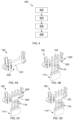
- FIG. 4 illustrates a flowchart for a method 400 of assembling the electrical device 300, namely, the connector 100, the electronic component 114, and the substrate 302 together.
- FIG. 5A, 5B, 5C, and 5D illustrates a step-by-step approach to assembling together the aforementioned components.
- FIG.s 5A, 5B, 5C and 5D The description that follows therefore pertain to the aforementioned figures in tandem.
- the connector 100 includes the main body 102.
- the main body 102 is preformed and the terminals 116 of the electronic component 114 is passed through the plurality of passages 200.
- the main body 102 is formed from two parts fused together with the terminals 116 being placed in between said two parts.
- FIG. 5A through 5D illustrates one such example where the main body 102 is formed from two parts.
- FIG. 5A illustrates a first part 500 of the two parts forming the main body 102.
- a second part 504 of said two parts is shown in FIG. 5C .
- the method 400 further includes a step 404 of placing the second part 504 on the terminals 116 so that the terminals 116 are sandwiched between the first part 500 and the second part 504, as depicted in FIG. 5C .
- the method 400 further includes a step 406 of fusing the second part 504 to the first part 500 of the connector 100.
- a fusing process such as, ultrasonic riveting
- the second part 504 is fused to the first part 500 thereby ensuring the terminals 116 are fixed, or assembled, to the connector 100.
- the connector 100 is formed of electrically insulating material, that is, the first part 500 and the second part 504 are formed from electrically insulating material; and, said parts 500, 504 brought in close proximity together, with the terminals sandwiched there-between, and melted by an application of heat or the like.
- the method 400 furthermore includes a step 408 of mounting the connector 100 to the bottom surface 306 of the substrate 302.
- the aforementioned step 408 of mounting includes inserting the at least two mounting legs 112 into the hole 308 formed on the substrate 302. More particularly, the one or more leg portions 112a, 112b, 112c is inserted through the hole 308.
- the insertion step in 408 is performed from when the detent shoulders 204a, 204b, 204c enters the substrate 302 from the bottom surface 306 and exits the top surface 304 via the hole 302. Accordingly, the contact surface 206 comes in contact with the top surface 304 of the substrate 302.
- the step 408 of inserting the leg portions 112a, 112b, 112c is performed till such a time the second contact surface 202 comes in contact with the bottom surface 306 of the substrate 302.
- the outcome configuration of the aforementioned step 408 of mounting the connector 100 to the substrate 302 is depicted in FIG. 3A and 3B .
- Such a substrate 302 may be a PCB of an electric power converter such as the one depicted in FIG. 3C , 3D and 3D .
- the connector 100 In the example where the electronic component 114 is a capacitor (or any other example electronic component 114 of the like) and the substrate 302 is a PCB, the connector 100, with the electronic component 114 fixed therein, the connector 100 is mounted onto the PCB in step 408.
- the second contact surface 202 of the at least one flange 201 come in contact with the bottom surface 306 of the PCB; and the contact surface(s) 206 of the detent shoulder(s) 204a, 204b, 204c come in contact with the opposite surface, i.e., the top surface 304, from which the detent shoulder(s) 204a, 204b, 204c exit.
- a stable mounting of the capacitor is achieved accordingly. Any axial and lateral play of the connector 100, and hence, the terminals 116 of the capacitor, is also largely mitigated. A process requiring holding the terminals of the capacitor for soldering is also eliminated.
Landscapes
- Engineering & Computer Science (AREA)
- Microelectronics & Electronic Packaging (AREA)
- Manufacturing & Machinery (AREA)
- Details Of Connecting Devices For Male And Female Coupling (AREA)
- Coupling Device And Connection With Printed Circuit (AREA)
Abstract
Description
- The present subject matter relates to a connector for an electronic component, more particularly, a connector for releasable mounting an electronic component to a substrate. The description herein pertains largely on such a connector for use in automotive applications.
- A variety of techniques to connect electronic components to a substrate, such as a PCB, is known. In a known manner, pins (or terminals) from the electronic components are passed through holes preformed in the substrate. The pins are then bent and fixed to the substrate, for instance, by means of soldering. At the time of mounting the electronic component in the above mentioned manner, the electronic component is held by a holding tool so that the pins may be soldered. If not held reliably, there is possibility of slippage of the pins during soldering.
- In another known technique, a positioning aid is used for positioning and holding the electronic components such that it can clamp the electronic component to the substrate. Such a positioning aid is disclosed in the prior art document
CN1 14172387A . The aforementioned prior art speaks of a positioning aid, made of plastic, to a half-bridge module on a heat sink. The positioning aid ofCN114172387A is non removable because it is permanently fixed to the heat sink. Such configurations are not easily serviceable if the need arises. Moreover, such configurations require that the pins be positioned precisely to penetrate into holes in the circuit board. Such technique is inefficient in terms of manufacturing process. Further, in case of an imprecise positioning, the pins may get damaged. - Therefore, the technical problem to be solved by the present subject matter is how to provide a connector that facilitate an efficient connection of electronic components to a substrate, ensuring mounting of the electronic component to be simple and involves fewer processes, whilst maintaining the structural integrity of the electronic component(s) and the connection.
- The present subject matter seeks to solve the above-mentioned technical problem in conventional connectors of electronic components. Such connectors may be applied to connect electronic components to a substrate for use in automotive applications. However, it is to be understood that the application is not limited to automotive applications alone.
- The present subject matter relates to a connector comprising: a main body having a substantially rectangular profile and comprising: a front face and a bottom face parallel to one another and a lateral face there-between; a plurality of passages adapted to receive terminals of an electronic component; and at least two mounting legs projecting perpendicularly from the front face of the main body, each of said mounting legs comprising a detent shoulder extending outwardly and defining a contact surface directed towards the front face of the main body. Accordingly, upon mounting the connector onto a substrate, such as a PCB, the at least two mounting legs facilitate the connector to a snap fit, or press fit, to said substrate. Further, the mounting of the connector is stabilized by virtue of the contact surface which is adapted to abut a surface of a substrate once said connector is mounted. Moreover, the connector holds the terminals of an electronic component in a robust manner so that the terminals do not require to be bend at the time of connecting terminals to a circuit formed on a substrate.
- According to an example of the present subject matter, one or more of the at least two mounting legs comprise one or more leg portions, wherein each of the one or more leg portions comprises one detent shoulder formed at a free end thereof. Such a configuration where a detent shoulder is provided for each of the one or more leg portions facilitate the connector to snap fit to a substrate. Moreover, the contact surface on each detent shoulder is configured to abut a surface of a substrate and stabilize the connector from axial and lateral play. Therefore, the terminals may be connected to an electric circuit integrated to a substrate with ease, without the terminals being held by a dedicated tool. Furthermore, it is to be noted that the detent shoulders may be oriented to face directions in relation to one another so that an effective fixture of the connector to a substrate may be achieved.
- According to an aspect of the present subject matter, the detent shoulder is formed in an arcuate shape. Such a shape permits the detent shoulder of each leg portion to pass through a hole in a substrate with ease.
- According to an aspect of the present subject matter, the at least one flange extends from the lateral face and defines a second contact surface parallel to the front face and bottom face, and directed to face the contact surface of the detent shoulder. Accordingly, in a configuration where the connector is snap fitted to a substrate, one surface of the substrate abuts the contact surface of the detent shoulders; and the other surface of the substrate abuts the second contact surface of the flange(s). Such a sandwiched configuration of the substrate ensures a robust fixture of the connector to such a substrate.
- According to an example of the present subject matter, the connector comprises two mounting legs, one on either side of the plurality of passages at the front face of the main body. In an aspect, one of two mounting legs aforementioned comprises two leg portions, and the other of the two mounting legs comprises one leg portion. Such a configuration ensures that the connector is supported at both ends, more particularly, at both ends of the plurality of passages, thereby ensuring structural stability of the connector upon being mounted. In one example, either of the two aforementioned mounting legs is cylindrically shaped.
- According to example, the connector is formed of electrically insulating material. Such a material may be plastic, and therefore, lightweight and cost effective.
- According to an example of the present subject matter, the main body comprises a first part and a second part fused together, and wherein the plurality of passages is formed there-between. Such a configuration ensures that the terminals are fixed robustly to the connector.
- The present subject matter relates also to an electrical device comprising: a substrate defining a top surface, a bottom surface, and an electric circuit printed in at least the top surface; and a connector, configured in accordance with the foregoing description, mounted on the bottom surface of the substrate, wherein terminals of an electronic component is received through the plurality of passages. Accordingly, electronic components in such an electric device may be mounted to the substrate in a simple and cost effective manner since a dedicated tool to hold the terminals is not required while connecting the terminals to the electric circuit. Moreover, the connector is fixed in a robust manner to restrict axial and lateral play, thereby ensuring structural integrity of the connection between the electronic component to the electric circuit.
- According to an example of the present subject matter, the electrical device is an electric power converter configured to convert electric power from alternating current (AC) to direct current (DC) and/or vice-versa.
- The present subject matter relates also to a method of assembling the electrical device, the method comprising: placing the terminals of the electronic component against a placement surface of the first part, the placement surface being lateral to the front face and the bottom face; placing the second part on the terminals and sandwiching said terminals between the first part and the second part; fusing the second part into the first part for fixture of the terminals to the connector; and mounting the connector to the bottom surface of the substrate, said step of mounting comprising: inserting the at least two mounting legs into a hole formed on the substrate so that the contact surface of the detent shoulder comes in contact with the top surface of the substrate. Accordingly, the terminals of the electronic component is fixed to the connector in a structurally robust manner; and the connector is mounted to the substrate with fewer methods involved. The assembling the aforementioned components in a production line may therefore be performed in an efficient and cost effective manner.
- According to an aspect of the present subject matter, the step of mounting the connector to the bottom surface further comprises the second contact surface coming in contact with the bottom surface of the substrate.
- The features, aspects, and advantages of the present invention will be better understood with regard to the following description and accompanying figures. The description refers to the annexed drawings, wherein:
-
FIG. 1 illustrates an isometric view of a connector for an electronic component, configured in accordance with the present subject matter; -
FIG. 2A illustrates the connector excluding the electronic component, configured in accordance with an aspect of the present subject matter; -
FIG. 2B illustrates the connector in another perspective view, the connector being configured in accordance with the present subject matter; -
FIG. 3A illustrates the connector mounted on a substrate for an electrical device, in accordance with an example of the present subject matter; and -
FIG. 3B illustrates a zoomed in view of the connector mounted on the substrate, as depicted inFIG. 3A , in accordance with an aspect of the present subject matter; -
FIG. 3C illustrates an electric power converter that includes the connector and the substrate on which said connector is mounted, in accordance with an example of the present subject matter; -
FIG. 3D illustrates a sectional view of the electric power converter, in accordance with the present subject matter; -
FIG. 3E illustrates zoomed in perspective of the electric power converter shown inFIG.3D , in accordance with the present subject matter; -
FIG. 4 illustrates a flowchart depicting a method of assembling the electronic component to the connector, in accordance with an example++ of the present subject matter; and -
FIG. 5A through 5D depict the connector at each step of the method illustrated inFIG. 4 , in accordance with an aspect of the present subject matter. - The figures are not necessarily to scale, and the size of some parts may be exaggerated to more clearly illustrate the example shown. Moreover, the drawings provide examples and/or examples consistent with the description, however, the description is not limited to the examples and/or examples provide in the drawings.
- In the description that follows, reference is made to accompanying drawings, which form part thereof, and in which is shown by way of illustration specific implementations in which the invention maybe practiced. These implementations are described in sufficient detail to enable that skilling in the art to practice the invention, and it is to be understood that the implementations may be combined, or that other implementations may be utilized, and that structural and logical changes may be made without departing from the scope of the present invention. The following detailed description is, therefore, not to be taken in a limiting sense, and the scope of the present invention is defined by the appended claims and their equivalents.
-
FIG. 1 illustrates aconnector 100, configured in accordance with the present subject matter. Theconnector 100 includes amain body 102 and at least two mountinglegs 112. Themain body 102 has a substantially rectangular profile and includes afront face 104 and abottom face 106 parallel to one another. Further, between the aforementioned twoflat faces front face 104 and thebottom face 106, is alateral face 108 formed there-between. Themain body 102 further includes a plurality of passages adapted to receiveterminals 116 of anelectronic component 114. The at least two mountinglegs 112 project perpendicularly from thefront face 104. Each of the mountinglegs 112 include a detent shoulder extending outwardly. The detent shoulder defines a contact surface that is directed towards thefront face 104 of themain body 102. - Accordingly, upon mounting the
connector 100 onto a substrate, such as a PCB, the at least two mountinglegs 112 facilitate theconnector 100 to a snap fit, or press fit, to said substrate. Further, the mounting of theconnector 100 is stabilized by virtue of the contact surface, of the detent shoulder, which is adapted to abut a surface of a substrate once saidconnector 100 is mounted. Moreover, theconnector 100, configured in accordance with the present subject matter, holds theterminals 116 of anelectronic component 114 in a robust manner so that theterminals 116 do not require to be bend at the time of connectingterminals 116 to a circuit formed on a substrate. Theelectronic component 114 referred herein may be a resistor or a capacitor or a transistor or a diode or an operational amplifier or a resistor array or a logic gate etc. - According to an example of the present subject matter, one or more of the at least two mounting
legs 112 is split into one ormore leg portions leg portion FIG. 1 , one of the at least two mountinglegs 112 has a cylindrical outer profile. Accordingly, in a scenario where theconnector 100 is to be mounted on a substrate, the detent shoulder(s) is configured to pass through a hole in the substrate to facilitate said mounting. -
FIG. 2A illustrates a perspective view of theconnector 100, configured in accordance with the present subject matter, in which theelectronic component 114 is excluded.FIG. 2B illustrates another perspective view of theconnector 100 excluding theelectronic component 114. For the sake of brevity, and due to similarity in reference numerals for both the aforementioned figures, the description provided herein pertains toFIG.s 2A and 2B in tandem. -
FIG. 2A and 2B depicts themain body 102 and plurality ofpassages 200 formed there-through. The plurality ofpassages 200permit terminals 114 of theelectronic component 114 through themain body 102. Preferable, theterminals 114 pass into the plurality ofpassages 200 from thebottom face 106 and exit from thefront face 104. In the example shown, mountinglegs 112, formed on thefront face 104, is provided on both sides of the plurality ofpassages 200. In the figures, there are two mountinglegs 112, one on either side of the plurality of passages 200.One of these mountinglegs 112 is split into twoleg portions leg 112 includes asingle leg portion 112c. The mountingleg 112 with twoleg portions legs 112 may include one ormore leg portions - According to the present subject matter, a
detent shoulder legs 112. In the examples depicted in figures, theconnector 100 includes two mountinglegs 112. one of the two mountinglegs 112 is split into twoleg portions leg portions detent shoulder leg 112 includes just oneleg portion 112c for which thedetent shoulder 204c if formed thereof. Eachdetent shoulder contact surface 206. Thecontact surface 206 on eachdetent shoulder front face 104 of themain body 102. The orientation of thedetent shoulders front face 104 of themain body 102. Therefore, upon mounting theconnector 100 to a substrate, the orientation of the contact surfaces 206 and thefront face 106 is such that said substrate is disposed there-between. In a non-limiting example, thedetent shoulders detent shoulders shoulders - According to an example of the present subject matter, the
connector 100 includesseveral leg portions 112. Someleg portions 112 are oriented in an opposite direction to each other. Some mounting leg are perpendicular to each other. In the examples depicted in figures, theleg portions leg portions leg portions leg portions connector 100 to a substrate. - According to an example of the present subject matter, the
connector 100 further includes at least oneflange 201 that extend from thelateral face 108 of themain body 102. The at least oneflange 201 defines asecond contact surface 202 parallel to the two flat faces, the two flat faces being thefront face 104 and thebottom face 106 of themain body 102. Thesecond contact surface 202 is oriented to be parallel to thecontact surface 206 of thedetent shoulders connector 100 may includeseveral flanges 201 distant from each other. In the example figures, there are threeflanges 201, each having thesecond contact surface 202 oriented to face thecontact surface 206 of the detent shoulder. Notably, for the mountingleg 112 that is split into twoleg portions dedicated flange 202. For the mounting 112 that has only oneleg portion 112c, there are twoflanges 202. Theflanges 202 are oriented so that thesecond contact surface 202 is facing thecontact surface 206. Accordingly, upon mounting theconnector 100 to a substrate, the substrate is sandwiched between thecontact surface 206 and thesecond contact surface 206. - According to an example, the
leg portions hole 208. Such a configuration with thehole 208 separates the twoleg portions leg portions -
FIG. 3A illustrates theconnector 100 mounted on asubstrate 302, configured in accordance with an example of the present subject matter.FIG. 3B is a zoomed in view of theconnector 100 mounted on thesubstrate 302, at 310 fromFIG. 3A. Figure 3C illustrates anelectrical device 300 in which theconnector 100 is applied, configured in accordance with an example of the present subject matter.FIG. 3D is a sectional view of theelectrical device 300, in accordance with the example shown inFIG. 3C .FIG. 3E is a zoomed in view of theconnector 100 mounted on thesubstrate 302 of the electrical device, in accordance with the example shown inFIG. 3C . For the sake of brevity, the description that follows pertain toFIG.s 3A, 3B, 3C ,3D and 3E in tandem. - According to an example, the
connector 100 is mounted on asubstrate 302, as shown inFIG. 3A . The detent shoulders 204a, 204b, 204c is passed through ahole 308 in thesubstrate 302 and exits from another side of thesubstrate 302. In a non-limiting example, thesubstrate 302 is a printed circuit board (PCB) where an electric circuit is integrated on at least one side of the PCB. Upon mounting theconnector 100 to thesubstrate 302, thesecond contact surface 206 abuts a surface of thesubstrate 302 from which thedetent shoulders hole 308. Accordingly, thesubstrate 302 sits between thecontact surface 206 of thedetent shoulder second contact surface 202 formed on the at least oneflange 201. Such a configuration ensures a stable mounting of theconnector 100 and hence, a reliable electric connection of the terminal 116 may be achieved with thesubstrate 302. Such anelectronic component 114 is any one of a resistor or a capacitor or a transistor or a diode or an operational amplifier or a resistor array or a logic gate etc., configured to electrically connect with the electric circuit integrated to thesubstrate 302. - Alternatively, the
connector 100 may be used as an interconnector (not shown), wherein the plurality ofpassages 200 are configured to fix interconnecting pins therein. These interconnecting pins may be male or female type pins that facilitate transfer of electric current or signals between two electrical devices, for instance, between an electric power converter and a DC-DC converter. Moreover, such aconnector 100, functioning as an interconnector, may be mounted on a PCB within an electrical device, such as, an electric power converter, a DC-DC converter, or a battery pack. - The present subject matter also relates to an
electrical device 300 that includes thesubstrate 302 and theconnector 100 as described above. In a non-limiting example, theelectric device 300 is an electric power converter for conversion of electric current from alternating current (AC) to direct current (DC) and/or vice-versa. Thesubstrate 302 has atop surface 304, abottom surface 306, and an electric circuit (not depicted). The electric circuit is printed in at least thetop surface 304 of thesubstrate 302. Theconnector 100, formed in the manner described above, is mounted from thebottom surface 306 of thesubstrate 302. Accordingly,terminals 116 of theelectronic component 114 is received through the plurality ofpassages 200 formed in theconnector 100. An electric connection between theelectronic component 114 and the electric circuit of thesubstrate 302 may be achieved for an effective conversion of AC to DC and/or vice-versa. -
FIG. 4 illustrates a flowchart for amethod 400 of assembling theelectrical device 300, namely, theconnector 100, theelectronic component 114, and thesubstrate 302 together.FIG. 5A, 5B, 5C, and 5D illustrates a step-by-step approach to assembling together the aforementioned components. For the sake of simplicity, the description forFIG. 4 can be read withFIG.s 5A, 5B, 5C and 5D . The description that follows therefore pertain to the aforementioned figures in tandem. - As described in the foregoing description, the
connector 100 includes themain body 102. As an example, themain body 102 is preformed and theterminals 116 of theelectronic component 114 is passed through the plurality ofpassages 200. In another example, themain body 102 is formed from two parts fused together with theterminals 116 being placed in between said two parts.FIG. 5A through 5D illustrates one such example where themain body 102 is formed from two parts.FIG. 5A illustrates afirst part 500 of the two parts forming themain body 102. Asecond part 504 of said two parts is shown inFIG. 5C . - According to an aspect of the present subject matter, the
method 400 of assembling theterminals 116 of theelectronic component 114 includes astep 402 of placing theterminals 116 against aplacement surface 502 of thefirst part 500. Theplacement surface 502 is oriented perpendicular to thefront face 104 and thebottom face 106. Therefore, in an aspect, during thestep 402 of placing theterminals 116, theelectronic component 114 is first oriented so that theterminals 116 are perpendicular to thefront face 104 and thebottom face 106; and then placed against theplacement surface 502. The outcome configuration of theaforementioned step 402 of placing theterminals 116 against theplacement surface 502 is depicted inFIG. 5B . - The
method 400 further includes astep 404 of placing thesecond part 504 on theterminals 116 so that theterminals 116 are sandwiched between thefirst part 500 and thesecond part 504, as depicted inFIG. 5C . Themethod 400 further includes astep 406 of fusing thesecond part 504 to thefirst part 500 of theconnector 100. By way of a fusing process, such as, ultrasonic riveting, in the step of 406, thesecond part 504 is fused to thefirst part 500 thereby ensuring theterminals 116 are fixed, or assembled, to theconnector 100. In a non-limiting way, theconnector 100 is formed of electrically insulating material, that is, thefirst part 500 and thesecond part 504 are formed from electrically insulating material; and, saidparts - According to the present subject matter, the
method 400 furthermore includes astep 408 of mounting theconnector 100 to thebottom surface 306 of thesubstrate 302. Theaforementioned step 408 of mounting includes inserting the at least two mountinglegs 112 into thehole 308 formed on thesubstrate 302. More particularly, the one ormore leg portions hole 308. The insertion step in 408 is performed from when thedetent shoulders substrate 302 from thebottom surface 306 and exits thetop surface 304 via thehole 302. Accordingly, thecontact surface 206 comes in contact with thetop surface 304 of thesubstrate 302. According to another aspect of the insertion step described above, thestep 408 of inserting theleg portions second contact surface 202 comes in contact with thebottom surface 306 of thesubstrate 302. The outcome configuration of theaforementioned step 408 of mounting theconnector 100 to thesubstrate 302 is depicted inFIG. 3A and 3B . Such asubstrate 302 may be a PCB of an electric power converter such as the one depicted inFIG. 3C ,3D and 3D . - In the example where the
electronic component 114 is a capacitor (or any other exampleelectronic component 114 of the like) and thesubstrate 302 is a PCB, theconnector 100, with theelectronic component 114 fixed therein, theconnector 100 is mounted onto the PCB instep 408. Upon mounting instep 408, thesecond contact surface 202 of the at least oneflange 201 come in contact with thebottom surface 306 of the PCB; and the contact surface(s) 206 of the detent shoulder(s) 204a, 204b, 204c come in contact with the opposite surface, i.e., thetop surface 304, from which the detent shoulder(s) 204a, 204b, 204c exit. A stable mounting of the capacitor is achieved accordingly. Any axial and lateral play of theconnector 100, and hence, theterminals 116 of the capacitor, is also largely mitigated. A process requiring holding the terminals of the capacitor for soldering is also eliminated. - Various modifications of the disclosed embodiments, as well as alternate embodiments of the subject matter, will become apparent to persons skilled in the art upon reference to the description of the subject matter. It is therefore contemplated that such modifications can be made without departing from the scope of the present subject matter is defined.
Claims (10)
- A connector (100) comprising:a main body (102) having a substantially rectangular profile and comprising:a front face (104) and a bottom face (106) parallel to one another and a lateral face (108) there-between;a plurality of passages (200) adapted to receive terminals (116) of an electronic component (114); andat least two mounting legs (112) projecting perpendicularly from the front face (104) of the main body (102), each of said mounting legs (112) comprising a detent shoulder (204a; 204b; 204c) extending outwardly and defining a contact surface (206) directed towards the front face (104) of the main body (102).
- The connector (100) as claimed in claim 1 wherein one or more of the at least two mounting legs (112) comprise one or more leg portions (112a; 112b; 112c), wherein each of the one or more leg portions (112a; 112b; 112c) comprises one detent shoulder (204a; 204b; 204c) formed at a free end thereof.
- The connector (100) as claimed in claim 2, wherein the detent shoulder (204a; 204b; 204c) is formed in an arcuate shape.
- The connector (100) as claimed in any one of the preceding claims, wherein at least one flange (201) extends from the lateral face (108) and defines a second contact surface (202) parallel to front face (104) and bottom face(106), and directed to face the contact surface (206) of the detent shoulder (204a; 204b; 204c).
- The connector (100), as claimed in any one of the preceding claims, is formed of electrically insulating material.
- The connector (100) as claimed in any one of the preceding claims, wherein the main body (102) comprises a first part (500) and a second part (504) fused together, and wherein the plurality of passages (200) is formed there-between.
- An electrical device (300) comprising:a substrate (302) defining a top surface (304), a bottom surface (306), and an electric circuit printed in at least the top surface (304); anda connector (100), as claimed in any one of the preceding claims, mounted on the bottom surface (306) of the substrate (302), wherein
terminals (116) of an electronic component (114) is received through the plurality of passages (200), - The electrical device (300) as claimed in claim 6, wherein the electrical device (300) is an electric power converter configured to convert electric power from alternating current (AC) to direct current (DC) and/or vice-versa.
- A method (400) of assembling the electrical device (300) configured in accordance with the previous claim, the method (400) comprising:placing the terminals (116) of the electronic component (114) against a placement surface (502) of the first part (500), the placement surface (502) being lateral to the front face (104) and the bottom face (106);placing the second part (504) on the terminals (116) and sandwiching said terminals (116) between the first part (500) and the second part (504);fusing the second part (504) into the first part (500) for fixture of the terminals (116) to the connector (100); andmounting the connector (100) to the bottom surface (306) of the substrate (302), said step of mounting comprising:
inserting the at least two mounting legs (112a; 112b; 112c) into a hole (208) formed on the substrate so that the contact surface (206) of the detent shoulder (204a; 204b; 204c) comes in contact with the top surface (304) of the substrate (302). - The method (400) as claimed in the preceding claim, wherein the step of mounting the connector (100) to the bottom surface (306) further comprises the second contact surface (202) coming in contact with the bottom surface (306) of the substrate (302).
Applications Claiming Priority (1)
| Application Number | Priority Date | Filing Date | Title |
|---|---|---|---|
| IN202341051782 | 2023-08-01 |
Publications (2)
| Publication Number | Publication Date |
|---|---|
| EP4503337A2 true EP4503337A2 (en) | 2025-02-05 |
| EP4503337A3 EP4503337A3 (en) | 2025-04-02 |
Family
ID=92142046
Family Applications (1)
| Application Number | Title | Priority Date | Filing Date |
|---|---|---|---|
| EP24191664.2A Pending EP4503337A3 (en) | 2023-08-01 | 2024-07-30 | A connector for an electronic component |
Country Status (1)
| Country | Link |
|---|---|
| EP (1) | EP4503337A3 (en) |
Citations (1)
| Publication number | Priority date | Publication date | Assignee | Title |
|---|---|---|---|---|
| CN114172387A (en) | 2020-09-11 | 2022-03-11 | 采埃孚股份公司 | Method for producing an inverter, positioning aid and inverter |
Family Cites Families (4)
| Publication number | Priority date | Publication date | Assignee | Title |
|---|---|---|---|---|
| US5344338A (en) * | 1992-03-04 | 1994-09-06 | Molex Incorporated | Strain relief structure for connecting flat flexible cable to a circuit board |
| GB2328329A (en) * | 1997-08-13 | 1999-02-17 | Ford Motor Co | Guiding pins for an electrical connection |
| EP3641067A1 (en) * | 2018-10-19 | 2020-04-22 | Quan Mei Technology Co. Ltd | Pin header |
| JP7155987B2 (en) * | 2018-12-14 | 2022-10-19 | 住友電装株式会社 | harness parts |
-
2024
- 2024-07-30 EP EP24191664.2A patent/EP4503337A3/en active Pending
Patent Citations (1)
| Publication number | Priority date | Publication date | Assignee | Title |
|---|---|---|---|---|
| CN114172387A (en) | 2020-09-11 | 2022-03-11 | 采埃孚股份公司 | Method for producing an inverter, positioning aid and inverter |
Also Published As
| Publication number | Publication date |
|---|---|
| EP4503337A3 (en) | 2025-04-02 |
Similar Documents
| Publication | Publication Date | Title |
|---|---|---|
| US7140885B2 (en) | Housing case for electronic circuit board | |
| US5254016A (en) | Interconnect device mounting apparatus for printed circuit boards | |
| US6080008A (en) | Push-wire contact | |
| CN105144433A (en) | Method for producing battery contact system and battery contact system | |
| JP2003257524A (en) | Electric connector | |
| US20100144177A1 (en) | Electrical connector with interlocking features | |
| US20230017724A1 (en) | High voltage contact system | |
| US20010010626A1 (en) | Substrate mount type terminal | |
| CN101305500A (en) | Printed circuit board stacking connector with separable joint | |
| US9407021B2 (en) | Compound cylinder PCB connection | |
| US20030060087A1 (en) | Terminal and connector using same | |
| EP4503337A2 (en) | A connector for an electronic component | |
| US8480412B2 (en) | Terminal and connector assembly | |
| KR20190048538A (en) | Connector for Connecting Board | |
| TWI333304B (en) | Ic socket | |
| EP0899830A2 (en) | Circuit card connector with isolation base assembly | |
| JPH10255930A (en) | Electric connector | |
| JP2002299000A (en) | Method of joining flexible printed circuit board and connection terminal | |
| JPH07161441A (en) | Surface mount type connector and manufacturing method thereof | |
| US20120129363A1 (en) | Electrical connector | |
| CN207338827U (en) | Connector | |
| TWI275206B (en) | Electrical connector | |
| JPH1126048A (en) | Terminal tool | |
| US12581588B2 (en) | Press-fit fasteners for securing components together | |
| JP2003032840A (en) | Electrical junction box |
Legal Events
| Date | Code | Title | Description |
|---|---|---|---|
| PUAI | Public reference made under article 153(3) epc to a published international application that has entered the european phase |
Free format text: ORIGINAL CODE: 0009012 |
|
| STAA | Information on the status of an ep patent application or granted ep patent |
Free format text: STATUS: REQUEST FOR EXAMINATION WAS MADE |
|
| 17P | Request for examination filed |
Effective date: 20240730 |
|
| AK | Designated contracting states |
Kind code of ref document: A2 Designated state(s): AL AT BE BG CH CY CZ DE DK EE ES FI FR GB GR HR HU IE IS IT LI LT LU LV MC ME MK MT NL NO PL PT RO RS SE SI SK SM TR |
|
| PUAL | Search report despatched |
Free format text: ORIGINAL CODE: 0009013 |
|
| AK | Designated contracting states |
Kind code of ref document: A3 Designated state(s): AL AT BE BG CH CY CZ DE DK EE ES FI FR GB GR HR HU IE IS IT LI LT LU LV MC ME MK MT NL NO PL PT RO RS SE SI SK SM TR |
|
| RIC1 | Information provided on ipc code assigned before grant |
Ipc: H01R 43/02 20060101ALI20250225BHEP Ipc: H05K 3/34 20060101ALI20250225BHEP Ipc: H01R 12/57 20110101ALI20250225BHEP Ipc: H01R 4/02 20060101AFI20250225BHEP |