EP4503289A1 - Battery module and electric device - Google Patents
Battery module and electric device Download PDFInfo
- Publication number
- EP4503289A1 EP4503289A1 EP22934267.0A EP22934267A EP4503289A1 EP 4503289 A1 EP4503289 A1 EP 4503289A1 EP 22934267 A EP22934267 A EP 22934267A EP 4503289 A1 EP4503289 A1 EP 4503289A1
- Authority
- EP
- European Patent Office
- Prior art keywords
- module
- battery
- battery pack
- housing
- inductor
- Prior art date
- Legal status (The legal status is an assumption and is not a legal conclusion. Google has not performed a legal analysis and makes no representation as to the accuracy of the status listed.)
- Pending
Links
Images


Classifications
-
- H—ELECTRICITY
- H01—ELECTRIC ELEMENTS
- H01M—PROCESSES OR MEANS, e.g. BATTERIES, FOR THE DIRECT CONVERSION OF CHEMICAL ENERGY INTO ELECTRICAL ENERGY
- H01M10/00—Secondary cells; Manufacture thereof
- H01M10/60—Heating or cooling; Temperature control
- H01M10/63—Control systems
-
- H—ELECTRICITY
- H01—ELECTRIC ELEMENTS
- H01M—PROCESSES OR MEANS, e.g. BATTERIES, FOR THE DIRECT CONVERSION OF CHEMICAL ENERGY INTO ELECTRICAL ENERGY
- H01M10/00—Secondary cells; Manufacture thereof
- H01M10/42—Methods or arrangements for servicing or maintenance of secondary cells or secondary half-cells
- H01M10/425—Structural combination with electronic components, e.g. electronic circuits integrated to the outside of the casing
-
- H—ELECTRICITY
- H01—ELECTRIC ELEMENTS
- H01M—PROCESSES OR MEANS, e.g. BATTERIES, FOR THE DIRECT CONVERSION OF CHEMICAL ENERGY INTO ELECTRICAL ENERGY
- H01M10/00—Secondary cells; Manufacture thereof
- H01M10/42—Methods or arrangements for servicing or maintenance of secondary cells or secondary half-cells
- H01M10/48—Accumulators combined with arrangements for measuring, testing or indicating the condition of cells, e.g. the level or density of the electrolyte
- H01M10/482—Accumulators combined with arrangements for measuring, testing or indicating the condition of cells, e.g. the level or density of the electrolyte for several batteries or cells simultaneously or sequentially
-
- H—ELECTRICITY
- H01—ELECTRIC ELEMENTS
- H01M—PROCESSES OR MEANS, e.g. BATTERIES, FOR THE DIRECT CONVERSION OF CHEMICAL ENERGY INTO ELECTRICAL ENERGY
- H01M10/00—Secondary cells; Manufacture thereof
- H01M10/42—Methods or arrangements for servicing or maintenance of secondary cells or secondary half-cells
- H01M10/48—Accumulators combined with arrangements for measuring, testing or indicating the condition of cells, e.g. the level or density of the electrolyte
- H01M10/486—Accumulators combined with arrangements for measuring, testing or indicating the condition of cells, e.g. the level or density of the electrolyte for measuring temperature
-
- H—ELECTRICITY
- H01—ELECTRIC ELEMENTS
- H01M—PROCESSES OR MEANS, e.g. BATTERIES, FOR THE DIRECT CONVERSION OF CHEMICAL ENERGY INTO ELECTRICAL ENERGY
- H01M10/00—Secondary cells; Manufacture thereof
- H01M10/60—Heating or cooling; Temperature control
- H01M10/65—Means for temperature control structurally associated with the cells
- H01M10/658—Means for temperature control structurally associated with the cells by thermal insulation or shielding
-
- H—ELECTRICITY
- H01—ELECTRIC ELEMENTS
- H01M—PROCESSES OR MEANS, e.g. BATTERIES, FOR THE DIRECT CONVERSION OF CHEMICAL ENERGY INTO ELECTRICAL ENERGY
- H01M50/00—Constructional details or processes of manufacture of the non-active parts of electrochemical cells other than fuel cells, e.g. hybrid cells
- H01M50/20—Mountings; Secondary casings or frames; Racks, modules or packs; Suspension devices; Shock absorbers; Transport or carrying devices; Holders
- H01M50/204—Racks, modules or packs for multiple batteries or multiple cells
-
- H—ELECTRICITY
- H01—ELECTRIC ELEMENTS
- H01M—PROCESSES OR MEANS, e.g. BATTERIES, FOR THE DIRECT CONVERSION OF CHEMICAL ENERGY INTO ELECTRICAL ENERGY
- H01M50/00—Constructional details or processes of manufacture of the non-active parts of electrochemical cells other than fuel cells, e.g. hybrid cells
- H01M50/20—Mountings; Secondary casings or frames; Racks, modules or packs; Suspension devices; Shock absorbers; Transport or carrying devices; Holders
- H01M50/284—Mountings; Secondary casings or frames; Racks, modules or packs; Suspension devices; Shock absorbers; Transport or carrying devices; Holders with incorporated circuit boards, e.g. printed circuit boards [PCB]
- H01M50/287—Fixing of circuit boards to lids or covers
-
- H—ELECTRICITY
- H01—ELECTRIC ELEMENTS
- H01M—PROCESSES OR MEANS, e.g. BATTERIES, FOR THE DIRECT CONVERSION OF CHEMICAL ENERGY INTO ELECTRICAL ENERGY
- H01M50/00—Constructional details or processes of manufacture of the non-active parts of electrochemical cells other than fuel cells, e.g. hybrid cells
- H01M50/50—Current conducting connections for cells or batteries
- H01M50/502—Interconnectors for connecting terminals of adjacent batteries; Interconnectors for connecting cells outside a battery casing
- H01M50/519—Interconnectors for connecting terminals of adjacent batteries; Interconnectors for connecting cells outside a battery casing comprising printed circuit boards [PCB]
-
- H—ELECTRICITY
- H01—ELECTRIC ELEMENTS
- H01M—PROCESSES OR MEANS, e.g. BATTERIES, FOR THE DIRECT CONVERSION OF CHEMICAL ENERGY INTO ELECTRICAL ENERGY
- H01M50/00—Constructional details or processes of manufacture of the non-active parts of electrochemical cells other than fuel cells, e.g. hybrid cells
- H01M50/50—Current conducting connections for cells or batteries
- H01M50/572—Means for preventing undesired use or discharge
-
- H—ELECTRICITY
- H01—ELECTRIC ELEMENTS
- H01M—PROCESSES OR MEANS, e.g. BATTERIES, FOR THE DIRECT CONVERSION OF CHEMICAL ENERGY INTO ELECTRICAL ENERGY
- H01M10/00—Secondary cells; Manufacture thereof
- H01M10/42—Methods or arrangements for servicing or maintenance of secondary cells or secondary half-cells
- H01M10/425—Structural combination with electronic components, e.g. electronic circuits integrated to the outside of the casing
- H01M2010/4271—Battery management systems including electronic circuits, e.g. control of current or voltage to keep battery in healthy state, cell balancing
-
- H—ELECTRICITY
- H01—ELECTRIC ELEMENTS
- H01M—PROCESSES OR MEANS, e.g. BATTERIES, FOR THE DIRECT CONVERSION OF CHEMICAL ENERGY INTO ELECTRICAL ENERGY
- H01M10/00—Secondary cells; Manufacture thereof
- H01M10/42—Methods or arrangements for servicing or maintenance of secondary cells or secondary half-cells
- H01M10/425—Structural combination with electronic components, e.g. electronic circuits integrated to the outside of the casing
- H01M2010/4278—Systems for data transfer from batteries, e.g. transfer of battery parameters to a controller, data transferred between battery controller and main controller
-
- Y—GENERAL TAGGING OF NEW TECHNOLOGICAL DEVELOPMENTS; GENERAL TAGGING OF CROSS-SECTIONAL TECHNOLOGIES SPANNING OVER SEVERAL SECTIONS OF THE IPC; TECHNICAL SUBJECTS COVERED BY FORMER USPC CROSS-REFERENCE ART COLLECTIONS [XRACs] AND DIGESTS
- Y02—TECHNOLOGIES OR APPLICATIONS FOR MITIGATION OR ADAPTATION AGAINST CLIMATE CHANGE
- Y02E—REDUCTION OF GREENHOUSE GAS [GHG] EMISSIONS, RELATED TO ENERGY GENERATION, TRANSMISSION OR DISTRIBUTION
- Y02E60/00—Enabling technologies; Technologies with a potential or indirect contribution to GHG emissions mitigation
- Y02E60/10—Energy storage using batteries
Definitions
- a rechargeable battery is a battery that is reusable after the active material is activated by charging the battery that is discharged.
- Rechargeable batteries are widely used in electronic devices such as mobile phones and laptop computers.
- a battery module typically includes a plurality of batteries to meet the voltage requirement of electronic devices.
- the battery releases heat during operation. How to improve the heat dissipation of the battery module and improve the charging and discharging performance of the battery module has always been a research topic in the industry.
- This application provides a battery module and an electrical device to improve heat dissipation of the battery module and improve the charging and discharging performance of the battery module.
- this application provides a battery module.
- the battery module includes a first housing, a second housing, a battery pack, and a circuit board.
- the first housing and the second housing are arranged along a first direction.
- the first housing includes a first recessed portion.
- the battery pack is disposed in the first recessed portion.
- the second housing includes a second recessed portion opposite to the first recessed portion.
- the second housing is connected to the first housing.
- the circuit board is disposed in the second recessed portion and is electrically connected to the battery pack.
- the circuit board is disposed in the second recessed portion of the second housing, all the peripheral walls of the second recessed portion can exchange heat with the circuit board, thereby increasing a heat exchange area between the circuit board and the second housing, shortening a heat conduction path between the circuit board and the second housing, improving heat dissipation efficiency of the circuit board, and improving the operating performance of the circuit board.
- the circuit board may be mounted and detached together with the second housing. During the use of the battery module, when the circuit board is faulty, the circuit board can be at least partially disconnected from the battery pack in a process of detaching the second housing, thereby simplifying the process of detaching the circuit board from the battery pack.
- the circuit board in assembling the battery module, can be connected to the battery pack during assembling of the first housing and the second housing, thereby simplifying the process of connecting the circuit board to the battery pack.
- This embodiment of this application can simplify the mounting and detachment process of the circuit board, save time for maintaining the battery module, and reduce cost.
- the circuit board includes a first surface on a side facing away from the battery pack in the first direction, and a second surface opposite to the first surface. The second surface facing towards the battery pack.
- a first module is disposed on the first surface of the circuit board.
- the first module is electrically connected to the battery pack and is configured to regulate an output power of the battery pack.
- the first module can connect the battery pack to an external charging cabinet or an external load.
- the first module includes a first inductor disposed on the first surface.
- the first inductor is configured to store energy.
- a control module is disposed on the first surface of the circuit board.
- the control module is configured to regulate the output power of the battery pack through the first module.
- the first module further includes a second inductor disposed on the first surface.
- the second inductor is configured to filter out common-mode interference at an output end of the battery module.
- the first inductor and the control module are arranged along a third direction, and the third direction is perpendicular to the first direction. When viewed from the first direction, on the first surface, the first inductor is located between the second inductor and the control module along the third direction, thereby meeting the loop requirements of devices and simplifying the wiring.
- the first module includes a capacitor disposed on the first surface.
- the capacitor is configured to store energy and provide output energy.
- the capacitor includes a first capacitor and a second capacitor.
- the first capacitor and the second capacitor are arranged along a third direction.
- the third direction is perpendicular to the first direction.
- the first inductor is located between the first capacitor and the second capacitor in the third direction.
- the first module includes a switch element disposed on the first surface.
- the switch element is configured to perform periodic switching.
- the second capacitor is located between the switch element and the control module in the third direction. The second capacitor can block the noise generated by the switch element during the switching, reduce the noise transmitted to the control module, and improve the operating environment of the control module.
- the first module further includes a third inductor.
- the third inductor may combine with the capacitor to form an inductor-capacitor (LC) filter circuit to suppress differential-mode interference generated by the switching voltage.
- LC inductor-capacitor
- a second module is disposed on the first surface of the circuit board.
- the second module is configured to acquire a signal and control charging and discharging of the battery pack.
- the battery module includes a first sampling piece.
- the first sampling piece is configured to acquire temperatures of the battery pack at a plurality of positions.
- the first sampling piece is connected to the sampling module.
- the battery pack includes a plurality of batteries.
- the battery module includes a second sampling piece.
- the second sampling piece is configured to acquire voltage of each of the batteries.
- the second sampling piece is connected to the sampling module.
- the second module includes a temperature control module.
- the temperature control module is configured to control working status of the battery pack based on a temperature of the battery pack.
- the battery module includes a heating element.
- the heating element is configured to heat the battery pack. Based on the temperature signal acquired by the sampling module, the temperature control module controls the heating element to turn on or off, so that the battery pack works within a preset temperature range.
- the first module includes a first interface
- the second module includes a second interface.
- the first interface is electrically connected to an electrical component outside the battery module.
- the second interface is communicatively connected to a control component outside the battery module.
- At least a part of the first module is covered by a first layer.
- the first layer includes an insulation material.
- the first layer can insulate at least a part of the first module from other components on the circuit board, thereby reducing short-circuiting risks and safety hazards.
- the first layer is connected to the bottom face of the second recessed portion to improve the connection strength between the circuit board and the second housing.
- the first layer includes a thermal adhesive.
- the first layer can conduct the heat generated by the first module to the second housing, thereby dissipating the heat and improving the performance and lifespan of the first module.
- the battery module in the first direction, includes a first plate, t the first plate and a bottom face of the second recessed portion together clamp the circuit board.
- the first plate and the bottom face of the second recessed portion clamp the circuit board to improve the stability of the circuit board.
- the battery pack includes a plurality of batteries.
- the plurality of batteries are stacked and arranged along a second direction perpendicular to the first direction.
- the battery pack includes a plurality of battery columns.
- the plurality of battery columns are arranged along a third direction.
- the third direction is perpendicular to the first direction and the second direction.
- Each of the battery columns includes a plurality of batteries stacked and arranged along the second direction.
- the battery pack is electrically connected to the circuit board by a first conductive portion.
- an embodiment of this application provides an electrical device.
- the electrical device includes the battery module disclosed in any one of the embodiments in the first aspect.
- the battery module is configured to provide electrical energy.
- connection may be a fixed connection, a detachable connection, or an integrated connection; or may be a direct connection or an indirect connection implemented through an intermediary; or may be internal communication between two components.
- parallel includes not only absolute parallelism, but also approximate parallelism conventionally known in engineering.
- perpendicular or “vertical” includes not only absolute perpendicularity, but also approximate perpendicularity conventionally known in engineering. As an example, if the angle between two directions is 80° to 90°, the two directions may be deemed perpendicular; and, if the angle between two directions is 0° to 10°, the two directions may be deemed parallel.
- FIG. 1 is a three-dimensional schematic structural diagram of a battery module according to an embodiment of this application
- FIG. 2 is a schematic exploded view of the battery module shown in FIG. 1
- FIG. 3 is another schematic exploded view of the battery module shown in FIG. 1
- FIG. 4 is another three-dimensional schematic structural diagram of the battery module shown in FIG. 1 , in which a second housing and a circuit board are omitted.
- the battery module in an embodiment of this application includes a first housing 3, a second housing 4, a battery pack 1, and a circuit board 2.
- the first housing 3 and the second housing 4 are disposed opposite to each other along the first direction Z.
- the first housing 3 includes a first recessed portion 31.
- the battery pack 1 is disposed in the first recessed portion 31.
- the second housing 4 includes a second recessed portion 41 opposite to the first recessed portion 31.
- the second housing 4 is connected to the first housing 3.
- the circuit board 2 is disposed in the second recessed portion 41 and is electrically connected to the battery pack 1.
- the circuit board 2 is disposed in the second recessed portion 41 of the second housing 4. All the peripheral walls of the second recessed portion 41 can exchange heat with the circuit board 2, thereby increasing a heat exchange area between the circuit board 2 and the second housing 4, shortening a heat conduction path between the circuit board 2 and the second housing 4, improving heat dissipation efficiency of the circuit board 2, and improving the operating performance of the circuit board 2.
- the circuit board 2 may be mounted and detached together with the second housing 4. During the use of the battery module, when the circuit board 2 is faulty, the circuit board 2 can be at least partially disconnected from the battery pack 1 in a process of detaching the second housing 4, thereby simplifying the process of detaching the circuit board 2 from the battery pack 1.
- the circuit board 2 in assembling the battery module, can be connected to the battery pack 1 during assembling of the first housing 3 and the second housing 4, thereby simplifying the process of connecting the circuit board 2 to the battery pack 1.
- This embodiment of this application can simplify the mounting and detachment process of the circuit board 2, save time for maintaining the battery module, and reduce cost.
- the first housing 3 and the second housing 4 may be connected into a whole by bonding, fastening, or other means to cover each other and jointly define an accommodation cavity configured to accommodate the battery pack 1 and the circuit board 2.
- the first housing 3 and the second housing 4 are connected by a fastener.
- the circuit board 2 is electrically connected to the battery pack 1 to control the charging and discharging of the battery pack 1.
- the circuit board 2 is fixed to the second housing 4.
- the circuit board 2 is fixed to the second housing 4 by a bonding layer.
- the bonding layer is thermally conductive.
- the bonding layer is formed by curing a thermal adhesive.
- the second housing 4 is made of metal.
- the second housing 4 is made of heat-conducting metal.
- the second housing 4 is made of aluminum alloy, copper alloy, steel, or another heat-conducting metal.
- the first housing 3 and the second housing 4 are disposed opposite to each other along the first direction Z.
- the battery pack 1 includes a plurality of batteries 111.
- the plurality of batteries 111 are stacked and arranged along a second direction X perpendicular to the first direction Z.
- the first surface 2a facing towards the bottom face 411 of the second recessed portion 41, and the second surface 2b facing towards the battery pack 1.
- the second module 22 includes a temperature control module 222.
- the temperature control module 222 is capable of regulating the temperature of the battery pack 1.
- the second module 22 further includes a control module 223.
- the control module 223 is capable of receiving and acquiring information or data such as temperature, voltage, and current, and issuing an instruction based on the received information, so as to implement functions such as battery charging and discharging, communication with external ECU devices, data storage, and fault alarm.
- the control module 223 includes a microcontroller unit (Microcontroller Unit, MCU).
- MCU microcontroller Unit
- the control module 223 includes a control IC.
- control module 223 feeds information back to and controls the temperature control module 222 based on the temperature signal acquired by the sampling module 221. Based on the instruction of the control module 223, the temperature control module 222 controls the heating element of the battery module to turn on or off, so as to make the battery work within the preset temperature range.
- the first module 21 includes a first interface 213.
- the second module 22 includes a second interface 214.
- the first interface 213 may be electrically connected to an electrical component outside the battery module.
- the second interface 214 may be communicatively connected to a control component outside the battery module.
- the battery pack 1 includes a first connector 45.
- the first connector 45 is disposed on the second housing 4.
- the first connector 45 is connected to the first interface 213. At least a part of the first connector 45 is located on outer shell of the second housing 4.
- the electrical component fits the first connector 45 in a pluggable manner to implement an electrical connection between the battery pack 1 and the electrical component.
- the first connector 45 includes a first socket.
- the electrical component is provided with a first plug mated to the first socket.
- the first inductor 211 and the control module 223 are arranged along a third direction Y.
- the third direction Y is perpendicular to the first direction Z.
- the first inductor 211 is located between the second inductor 218 and the control module 223 along the third direction Y, thereby meeting the loop requirements of devices and simplifying the wiring.
- the capacitor 212 includes a first capacitor 2121 and a second capacitor 2122.
- the first inductor 211 is located between the first capacitor 2121 and the second capacitor 2122 in the third direction Y.
- the second capacitor 2122 when viewed from the first direction Z, on the first surface 2a, the second capacitor 2122 is located between the switch element 216 and the control module 223 in the third direction Y.
- the second capacitor 2122 can block the noise generated by the switch element 216 during the switching, reduce the noise transmitted to the control module 223, and improve the operating environment of the control module 223.
- the first module 21 is covered by a first layer 5.
- the first layer 5 includes an insulation material.
- the first layer 5 includes a potting glue.
- the first layer 5 includes a thermal adhesive.
- the thermal adhesive may be organic thermal silicone, epoxy resin AB adhesive, polyurethane adhesive, or another type of thermal silicone.
- the first layer 5 can insulate at least a part of the first module 21 from other components on the circuit board 2, thereby reducing short-circuiting risks and safety hazards.
- the circuit board 2 is connected to the second housing 4 through the first layer 5.
- the first layer 5 is connected to the first surface 2a of the circuit board 2 as well as the sidewall and the bottom wall of the second recessed portion 41.
- the first layer 5 covers the first inductor 211, the capacitor 212, the first interface 213, the second interface 214, the connecting terminal 215, the switch element 216, the second inductor 218, and the third inductor 219.
- the term "covering" means partially covering or fully covering.
- the first layer 5 covers at least a part of the second module 22 to insulate at least a part of the second module 22 from other components on the circuit board 2.
- the first layer 5 covers the sampling module 221, the temperature control module 222, and the control module 223.
- the first layer 5 is connected to the bottom face 411 of the second recessed portion 41. In these embodiments, the first layer 5 can connect the first module 21 to the bottom face 411 of the second recessed portion 41 to improve the connection strength between the circuit board 2 and the second housing 4.
- the first layer 5 is made of an insulating thermal material.
- the first layer 5 can conduct the heat generated by the first module 21 to the second housing 4, thereby dissipating the heat and improving the performance and lifespan of the first module 21.
- the first layer 5 is formed by curing a thermal adhesive.
- a thermal conductor 24 is disposed on the first surface 2a of the circuit board 2.
- the thermal conductor 24 may directly abut the bottom face 411 of the second recessed portion 41, or may be connected to the bottom face through the first layer 5.
- the thermal conductor 24 can conduct the heat generated by the circuit board 2 to the second housing 4.
- the thermal conductor 24 is made of aluminum.
- the thermal conductor 24 is disposed on both sides of the first inductor 211.
- the switch element 216 is mounted on the thermal conductor 24.
- the heat generated by the switch element 216 can be conducted to the second housing 4 through the thermal conductor 24.
- the height by which the first inductor 211 protrudes beyond the circuit board 2 is greater than the height by which the sampling module 221 protrudes beyond the circuit board 2.
- the heat generated by the first inductor 211 is higher than the heat generated by the sampling module 221.
- the height of the capacitor 212, the height of the first interface 213, the height of the second interface 214, the height of the second inductor 218, and the height of the third inductor 219 are all greater than the height of the sampling module 221.
- the height h1 by which the first inductor 211 protrudes beyond the circuit board 2 is greater than the height h6 by which the temperature control module 222 protrudes beyond the circuit board 2.
- the first inductor 211 can store energy and provide output energy during the charging and discharging.
- the current flowing through the first inductor 211 is relatively large.
- the amount of heat generated by the first inductor 211 is relatively large.
- the relatively large height h1 of the first inductor 211 can reduce the distance between the first inductor 211 and the bottom wall of the second recessed portion 41, so as to increase the heat exchange rate between the first inductor 211 and the bottom wall of the second recessed portion 41, and improve the heat dissipation of the first inductor 211.
- the current flowing through the temperature control module 222 is relatively small, and the amount of heat generated by the temperature control module 222 is relatively small.
- the relatively small height h6 of the temperature control module 222 can increase the distance between the temperature control module 222 and the bottom wall of the second recessed portion 41, and reduce the heat conducted to the temperature control module 222 through the bottom wall of the second recessed portion 41.
- the height h2 by which the first capacitor 2121 protrudes beyond the circuit board 2, the height h3 by which the switch element 216 protrudes beyond the circuit board 2, the height h4 by which the second inductor 218 protrudes beyond the circuit board 2, and the height h5 by which the third inductor 219 protrudes beyond the circuit board 2 are all greater than the height h6 by which the temperature control module 222 protrudes beyond the circuit board 2.
- the current flowing through the first capacitor 2121, the switch element 216, the second inductor 218, and the third inductor 219 is relatively large.
- the heat generated by such components is relatively high.
- the relatively large height of such components can improve the heat dissipation efficiency.
- the battery module in the first direction Z, includes a first plate 6, the first plate 6 and a bottom face 411 of the second recessed portion 41together clamp the circuit board 2.
- the first plate 6 and the bottom face 411 of the second recessed portion 41 clamp the circuit board 2 to improve the stability of the circuit board 2.
- the second housing 4 includes a protruding portion 42 that protrudes beyond the bottom face 411 of the second recessed portion 41.
- the protruding portion 42 abuts against the first surface 2a.
- the protruding portion 42 and the first plate 6 clamp the circuit board 2 from both sides, and the space between the first surface 2a and the bottom face 411 of the second recessed portion 41 can accommodate the first module 21 and the second module 22.
- the battery module includes a fastener 8.
- the fastener 8 passes through the first plate 6 and the circuit board 2, and is threadedly connected to the protruding portion 42 to fix the circuit board 2 to the second housing 4.
- an insulation layer is disposed on a surface, facing toward the circuit board 2, of the first plate 6 to insulate the first plate 6 from the circuit board 2.
- the first plate 6 is an aluminum sheet.
- the aluminum sheet facilitates heat dissipation of the circuit board 2.
- the battery pack 1 is electrically connected to the circuit board 2 by a first conductive portion 7.
- the first conductive portion 7 fits the connecting terminal 215 in a pluggable manner.
- the first conductive portion 7 is directly plug-in connected to the connecting terminal 215, thereby reducing the need of other fixing structures, and facilitating the mounting and detachment of the circuit board 2.
- the circuit board 2 is provided with a first through-hole 23, and the first plate 6 is provided with a second through-hole 61.
- the first through-hole 23 and the second through-hole 61 are disposed opposite to each other along the first direction Z.
- the first conductive portion 7 can pass through the second through-hole 61 and the first through-hole 23 so as to be plug-in connected to the connecting terminal 215.
- components such as the circuit board 2, the second housing 4, and the first plate 6 can be assembled together beforehand to form a housing assembly 100.
- the circuit board 2 and the second housing 4 form a one-piece structure to facilitate mounting and detachment.
- an insulation piece 62 is disposed on one side, facing away from the circuit board 2, of the first board 6.
- the insulation piece 62 is provided with a third through-hole 63.
- the third through-hole 63 is opposite to the second through-hole 61 along the first direction Z.
- the first conductive portion 7 passes through the third through-hole 63, the second through-hole 61, and the first through-hole 23 so as to be plug-in connected to the connecting terminal 215.
- the battery module further includes an insulation component 10.
- the insulation component 10 covers at least a part of the battery pack 1. After the second housing 4 is detached, the insulation component 10 can insulate the battery pack 1 from the staff, thereby reducing the risk of the staff contacting the power circuit and improving safety.
- the insulation component 10 includes an insulation body 10a and an insulation bulge 10b that protrudes beyond the insulation body 10a.
- the first conductive portion 7 passes through the insulation body 10a.
- the insulation bulge 10b surrounds the first conductive portion 7 from the outside. After the second housing 4 is detached, the insulation bulge 10b can insulate the first conductive portion 7 from the staff, thereby reducing the risk of the staff contacting the power circuit.
- the insulation bulge 10b may be an annular structure, a U-shaped structure, or a semicircular structure.
- the first conductive portion 7 passes through the insulation bulge 10b of the insulation component 10, the third through-hole 63, the second through-hole 61, and the first through-hole 23 sequentially to pass through the circuit board 2 and be plug-in connected to the connecting terminal 215.
- two first conductive portions 7 and two connecting terminals 215 are disposed.
- One of the first conductive portions 7 is connected to one connecting terminal 215 and a main positive output electrode of the battery pack.
- the other first conductive portion 7 is connected to the other connecting terminal 215 and a main negative output electrode of the battery pack.
- the battery module further includes a first harness 9.
- the first harness 9 may be electrically connected to the sampling module 221.
- the first harness 9 can connect the first sampling piece and the sampling module 221.
- the first sampling piece includes a temperature probe.
- a battery 111 includes a battery housing, an electrode assembly, and an electrolyte solution.
- the electrode assembly and the electrolyte solution are accommodated in the battery housing.
- the electrode assembly includes a positive electrode plate, a negative electrode plate, and a separator.
- the battery 111 works primarily by shuttling metal ions between the positive electrode plate and the negative electrode plate.
- the plurality of batteries 111 may be connected in series, parallel, or series-and-parallel pattern.
- the series-and-parallel pattern means a combination of series connection and parallel connection of the plurality of batteries 111.
- the battery pack 1 further includes a first bracket 12 and a second bracket 13.
- the first bracket 12 is disposed at one end, close to the second housing 4, of the battery 111 and is connected to the battery 111.
- the second bracket 13 is disposed at one end, facing away from the second housing 4, of the battery 111 and is connected to the battery 111.
- the first bracket 12 and the second bracket 13 are accommodated in the first recessed portion 31 and can support and fix the battery 111.
- the battery pack 1 includes a plurality of battery columns 11.
- the plurality of battery columns 11 are arranged along a third direction Y
- the third direction Y is perpendicular to the first direction Z and the second direction X.
- Each of the battery columns 11 includes a plurality of batteries 111 stacked and arranged along the second direction X.
- a plurality of fins 43 are disposed on the outer side of the second housing 4.
- the fins 43 can increase the surface area of the second housing 4, improve the heat dissipation efficiency of the second housing 4, and ensure the safety of the electronic components.
- the second housing 4 is provided with a positioning pin 44.
- the positioning pin 44 can guide insertion of the second housing 4 into the first housing 3 to implement positioning of the second housing 4 and the first housing 3, and enable accurate plug-in connection between the first conductive portion 7 and the connecting terminal 215.
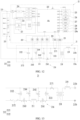
- system composition and circuit diagram of a battery module are described below with reference to FIG. 12 .
- the system composition and circuit diagram of the battery module shown in FIG. 12 are not limited to exactly the same components as those in FIG. 12 , but may be flexibly applied based on the relevant knowledge of a person skilled in the art.
- the battery management system is provided with a first module 21 and a second module 22.
- the first module 21 serves a function of regulating the output power of the battery pack 1.
- the second module 22 serves a function of acquiring a signal and controlling the charging and discharging of the battery pack 1.
- the second module 22 can control the first module 21.
- the first module 21 is a charge-discharge power supply circuit module, and is capable of connecting the battery pack 1 to an external charging cabinet or an external load (such as a vacuum cleaner, a laptop computer, or an electric tool).
- the first module 21 serves a buck-boost function.
- the first module 21 includes a buck-boost circuit (a circuit for stepping up and down voltage) configured to regulate internal and external voltages.
- the current flowing through the first module 21 is relatively large.
- the heat generated by the first module 21 is higher than the heat generated by the second module 22.
- the second module 22 includes a power supply circuit 224, a control module 223, a sampling module 221, and a temperature control module 222.
- the power supply circuit 224 is connected to the control module 223 and the battery pack 1, so as to transmit the voltage and current of the battery pack 1 to the control module 223 as a power supply.
- the sampling module 221 can acquire information about the battery, and upload the information to the control module 223.
- the sampling module 221 can acquire the information such as the voltage and temperature of the battery of the battery pack 1.
- the control module 223 is configured to receive and acquire the information or data such as temperature, voltage, and current, and issue an instruction based on the received information, so as to implement functions such as battery charging and discharging, communication with external ECU devices, data storage, and fault alarm.
- the control module 223 can regulate the temperature of the battery through the temperature control module 222 based on the data information uploaded by the sampling module 221.
- the control module 223 can also control the first module 21 to regulate the output power of the battery pack 1 through the first module 21.
- control module 223 includes a microcontroller unit (Microcontroller Unit, MCU).
- MCU Microcontroller Unit
- the second module 22 may further include a communication module 225.
- the communication module 225 may be connected to the control module 223 and an external ECU device to implement communication between the control module 223 and the external ECU device.
- the communication module 225 may include a second connector 214.
- the second module 22 may further include an indicator light 226.
- the indicator light 226 may serve a function of displaying the power status of the battery and the operating status of the battery management system.
- the indicator light 226 is an LED indicator.
- the second module 22 may further include a data storage module 227.
- the data storage module 227 may serve a function of storing the operating data of the battery management system.
- the data storage module 227 includes a memory chip.
- the memory chip may serve a function of storing data information.
- the second module 22 further includes a hardware watchdog module 228.
- the hardware watchdog module 228 works together with the control module 223 to avoid software runaway.
- the second module 22 may further include a clock module 229.
- the clock module 229 provides real-time clock data for the control module 223.
- the second module 22 may further include an alarm module 229a.
- the alarm module 229a may serve a function of sending an alarm message when the battery management system is abnormal.
- the alarm module 229a includes a buzzer.
- the second module 22 includes a voltage acquisition module 251 and a current acquisition module 252.
- the voltage acquisition module serves a function of detecting the voltage output by the battery module.
- the current acquisition module 252 serves a function of detecting the current output by the battery module.
- the second module 22 further includes a control drive circuit 253.
- the control drive circuit 253 may be connected to the control module 223 and the first module 21 to control a buck-boost circuit of the first module 21.
- the first module 21 may include a switch element 216, a capacitor 212, a first inductor 211, a second inductor 218, and a third inductor 219.
- the switch element 216 serves a function of performing periodic switching to generate desired voltage and current.
- the switch element 216 can make a circuit when the control drive circuit 253 outputs a valid drive signal, and break the circuit when the control drive circuit 253 cuts off the valid drive signal.
- the switch element 216 may be a transistor.
- the transistor may be a bipolar transistor, a field effect transistor (MOS), an insulated gate bipolar transistor (IGBT), or another type of transistor.
- the capacitor 212 may serve a function of filtering out interference, storing energy, and reducing loop current ripples.
- the first inductor 211 may be a power inductor.
- the second inductor 218 serves a function of filtering out common-mode interference at a positive output end and a negative output end of the battery module to improve the EMC of the circuit.
- the second inductor 218 is a common-mode inductor.
- the third inductor 219 combines with the capacitor 212 to form an LC filter circuit to suppress differential-mode interference generated by the switching voltage.
- the third inductor 219 may be a differential-mode inductor.
- the first module 21 is provided with a first output end 213a and a second output end 213b.
- the first output end 213a may be connected to a positive electrode of a charger or a load (such as a vacuum cleaner) through a first connector.
- the second output end 213b may be connected to a negative electrode of the charger or the load through the first connector.
- the first output end 213a and the second output end 213b may be connectors.
- the first module 21 is provided with a resistor element 2171.
- the current acquisition module 252 can acquire the current value at the resistor element 2171.
- At least four switch elements 216 are disposed.
- the four switch elements 216 are defined as: a first switch element 2161, a second switch element 2162, a third switch element 2163, and a fourth switch element 2164, respectively.
- the first switch element 2161, the second switch element 2162, the third switch element 2163, and the fourth switch element 2164 may be N-type MOS.
- the first switch element 2161, the second switch element 2162, the third switch element 2163, and the fourth switch element 2164 may be P-type MOS.
- At least four capacitors 212 are disposed, of which two capacitors 212 are defined as a first capacitor 2121 and a second capacitor 2122 respectively.
- the first end of the third inductor 219 is connected to the second output end 213b, that is, connected to the negative electrode of the charger or the load.
- the second end of the third inductor 219 is connected to the first end of the second inductor 218.
- the second end of the second inductor 218 is connected to the second end of the resistor element 2171.
- the third end of the second inductor 218 is connected to the first end of the first capacitor 2121 and the third end of the first switch element 2161.
- the fourth end of the second inductor 218 is connected to the first output end, that is, connected to the positive electrode of the charger or the load.
- the third end of the first switch element 2161 is connected to the first end of the first capacitor 2121.
- the first end of the first switch element 2161 is connected to the output end of the control drive circuit 253.
- the second end of the first switch element 2161 is connected to the second end of the first inductor 211 and the second end of the second switch element 2162.
- the third end of the second switch element 2162 is connected to the negative output electrode of the battery pack 1.
- the first end of the second switch element 2162 is connected to the output end of the control drive circuit 253.
- the first end of the first inductor 211 is connected to the third end of the third switch element 2163 and the second end of the fourth switch element 2164.
- the third end of the fourth switch element 2164 is connected to the negative output electrode of the battery pack 1.
- the first end of the third switch element 2163 and the first end of the fourth switch element 2164 are connected to the output end of the control drive circuit 253 separately.
- Each switch element is driven to turn on by an effective drive signal output by the control drive circuit 253, and is driven to turn off by cutting off the effective drive signal.
- the second end of the third switch element 2163 is connected to the first end of the second capacitor 2122 and the second end of the fusing element 2172.
- the second end of the first capacitor 2121 and the second end of the second capacitor 2122 are both connected to the negative output electrode of the battery pack 1.
- the first end of the fusing element 2172 is connected to the positive output electrode of the battery pack 1, and is connected in series in a positive output electrode loop of the battery pack 1 to implement protection against overcurrent and short-circuiting.
- the first end of the resistor element 2171 is connected to the second end of the first capacitor 2121 and the negative output electrode of the battery pack 1.
- the current acquisition module 252 is connected to the first end and the second end of the resistor element 2171.
- first end, second end, third end, and fourth end involved in each component are identified by numbers 1, 2, 3 and 4, respectively, near the corresponding component.
- the voltage acquisition module 251 is connected to a first output end 213a and a second output end 213b.
- the battery module in an embodiment of this application works in at least the following four operating conditions.
- the control module 223 When the control module 223 detects, through the voltage acquisition module 251, that V p + is greater than V b + during charging of the battery module, the first module 21 enters a buck charging mode. In this case, the control module 223 controls, through the control drive circuit 253, the third switch element 2163 to close and the fourth switch element 2164 to open, and then the first switch element 2161, the second switch element 2162, the first capacitor 2121, the second capacitor 2122, and the first inductor 211 form a synchronous buck circuit topology.
- the buck power supply switches the first switch element 2161 and the second switch element 2162 at a fixed frequency, and adjusts the duty cycle to implement the function of buck constant-current charging.
- step (I) is performed before step (II).
- the control drive circuit 253 controls the second switch element 2162 to open and controls the first switch element 2161 to close.
- the current flows from the first output end 213a through the second inductor 218, the first switch element 2161, and the first inductor 211 successively, and then flows through the third switch element 2163 and the fusing element 2172 to the positive output electrode of the battery pack 1.
- the first output end 213a and the second output end 213b input a voltage to the first inductor 211, the second capacitor 2122, and the battery to perform charging. At this time, the first inductor 211 and the second capacitor 2122 store energy.
- step (II) the control drive circuit 253 controls the first switch element 2161 to open and the second switch element 2162 to close. Because the current of the first inductor 211 needs to avoid abrupt change, the current of the first inductor 211 flows from the first end 211a of the first inductor 211 through the third switch element 2163 and the fusing element 2172 to the positive output electrode of the battery pack 1.
- the current flows from the positive output electrode of the battery pack 1 to the negative output electrode of the battery pack 1, and then flows from the negative output electrode of the battery pack 1 through the second switch element 2162 to the second end 211b of the first inductor 211, thereby completing the process of discharging and freewheeling of the inductor and charging the battery.
- step (II) freewheeling and charging are maintained by relying solely on the energy stored in the first inductor 211. Therefore, the average output voltage is less than the input voltage in one cycle, so that the circuit module implements the buck charging function. Steps (I) and (II) are repeated cyclically to implement stepped-down stable voltage output.
- the time in step (I) is ti
- the time in step (II) is t 2
- the value of t 1 /(t 1 + t 2 ) is a switching duty cycle D.
- the current value detected by the current acquisition module 252 is I p + and the system sets the charging current limit value to I c +
- the duty cycle D is reduced; when I p + is less than I c + , the duty cycle D is increased.
- I p + is equal to I c +
- the duty cycle D remains unchanged.
- the switch element 216 incurs a conduction loss and a switching loss.
- the current of the circuit is relatively large, and the switching frequency is relatively high.
- the loss is accumulated during the switching.
- the loss is converted into heat. Therefore, the switch element 216 generates heat intensely.
- the first layer in the embodiment of this application can transmit the heat generated by the switch element 216 to the second housing, so as to dissipate heat for the switch element 216, and improve the performance and lifespan of the switch element 216.
- the control module 223 When the control module 223 detects, through the voltage acquisition module 251, that V p + is less than or equal to V b + during charging of the battery module, the first module 21 enters a boost charging mode. In this case, the control module 223 controls, through the control drive circuit 253, the first switch element 2161 to close and the second switch element 2162 to open, and then the third switch element 2163, the fourth switch element 2164, the first capacitor 2121, the second capacitor 2122, and the first inductor 211 form a boost circuit topology.
- the boost power supply switches the third switch element 2163 and the fourth switch element 2164 at a fixed frequency, and adjusts the duty cycle to implement the function of boost constant-current charging.
- step (I) is performed before step (II).
- step (I) the control drive circuit 253 controls the third switch element 2163 to open and the fourth switch element 2164 to close.
- the current flows from the first output end 213a through the second inductor 218, the first switch element 2161, and the first inductor 211 successively, and then flows through the fourth switch element 2164 to the negative output electrode of the battery pack 1.
- the first output end 213a and the second output end 213b input a voltage to the first inductor 211 to perform charging. At this time, the first inductor 211 stores energy.
- step (II) the control drive circuit 253 controls the fourth switch element 2164 to open and the third switch element 2163 to close.
- the current of the first inductor 211 needs to avoid abrupt change, the current of the first inductor 211 flows from the first end 211a of the first inductor 211 through the third switch element 2163 and then through the fusing element 2172 to the positive output electrode of the battery pack 1 to charge the battery and the second capacitor 2122.
- the voltage between the two ends of the second capacitor 2122 is V p + plus the voltage between the two ends of the first inductor 211. Therefore, the charging output voltage at this time is already higher than the input voltage, thereby implementing the function of boost charging. Steps (I) and (II) are repeated cyclically to implement stepped-up stable voltage output.
- the constant-current charging function is implemented by adjusting the duty cycle D of the output of the control drive circuit 253.
- the implementation process is the same as that described in circuit condition I.
- the control module 223 When the control module 223 detects, through the voltage acquisition module 251, that V b + is less than or equal to V p + during discharging of the battery module, the first module 21 enters a boost discharging mode. In this case, the control module 223 controls, through the control drive circuit 253, the third switch element 2163 to close and the fourth switch element 2164 to open, and then the first switch element 2161, the second switch element 2162, the first capacitor 2121, the second capacitor 2122, and the first inductor 211 form a synchronous boost circuit topology.
- the boost power supply switches the first switch element 2161 and the second switch element 2162 at a fixed frequency, and adjusts the duty cycle to implement the function of boost constant-current discharging.
- step (I) is performed before step (II).
- the control drive circuit 253 controls the first switch element 2161 to open and the second switch element 2162 to close.
- the current flows from the positive output electrode of the battery pack 1 through the fusing element 2172, the third switch element 2163, and the first inductor 211 successively, and then flows through the second switch element 2162 to the negative output electrode of the battery pack 1.
- the positive output electrode of the battery pack 1 and the negative output electrode of the battery pack 1 input a voltage to the first inductor 211 to perform charging. At this time, the first inductor 211 stores energy.
- step (II) the control drive circuit 253 controls the second switch element 2162 to open and the first switch element 2161 to close. Because the current of the first inductor 211 needs to avoid abrupt change, the current of the first inductor 211 flows from the second end 211b of the first inductor 211 through the first switch element 2161 to charge the first capacitor 2121, and then flows through the second inductor 218 to the first output end 213a to charge the load. At this time, the voltage across the first output end 213a and the voltage across the second output end 213b are V b + plus the voltage between the two ends of the first inductor 211. Therefore, the discharging output voltage at this time is already higher than the input voltage, thereby implementing the function of boost discharging. Steps (I) and (II) are repeated cyclically to implement stepped-up stable voltage output.
- the constant-current charging function is implemented by adjusting the duty cycle D of the output of the control drive circuit 253.
- the implementation process is the same as that described in circuit condition I.
- the control module 223 When the control module 223 detects, through the voltage acquisition module 251, that V b + is greater than V p + during discharging of the battery module, the first module 21 enters a buck discharging mode. In this case, the control module 223 controls, through the control drive circuit 253, the first switch element 2161 to close and the second switch element 2162 to open, and then the third switch element 2163, the fourth switch element 2164, the first capacitor 2121, the second capacitor 2122, and the first inductor 211 form a synchronous buck circuit topology.
- the buck power supply switches the third switch element 2163 and the fourth switch element 2164 at a fixed frequency, and adjusts the duty cycle to implement the function of buck constant-current discharging.
- step (I) is performed before step (II).
- the control drive circuit 253 controls the fourth switch element 2164 to open and the third switch element 2163 to close.
- the current flows from the positive output electrode of the battery pack 1 through the fusing element 2172, the third switch element 2163, and the first inductor 211 successively, and then flows through the first switch element 2161 and the second inductor 218 to the first output end 213a.
- the positive output electrode of the battery pack 1 and the negative output electrode of the battery pack 1 input a voltage to the first inductor 211 and the first capacitor 2121 to perform charging and discharge the load. At this time, the first inductor 211 and the first capacitor 2121 store energy.
- step (II) the control drive circuit 253 controls the third switch element 2163 to open and the fourth switch element 2164 to close. Because the current of the first inductor 211 needs to avoid abrupt change, the current of the first inductor 211 flows from the second end 211b of the first inductor 211 through the first switch element 2161 to charge the first capacitor 2121, and then flows through the second inductor 218 to the first output end 213a to power the load. Subsequently, the current flows back to the second output end 213b, flows through the third inductor 219, the second inductor 218, and the resistor element 2171 successively.
- step (II) the freewheeling and discharging of the inductor are maintained by relying on the energy stored in the inductor. Therefore, the average output voltage is less than the input voltage in one cycle, so that the circuit module implements the buck discharging function. Steps (I) and (II) are repeated cyclically to implement stepped-down stable voltage output.
- the constant-current charging function is implemented by adjusting the duty cycle D of the output of the control drive circuit 253.
- the implementation process is the same as that described in circuit condition I.
- the electrical device includes the battery module disclosed in any one of the above embodiments.
- the battery module is configured to provide electrical energy.
- the electrical device may be a mobile phone, a portable device, a laptop computer, an electric toy, an electric tool, a micro base station, or the like.
- the electric tool may be a metal cutting electric tool, a cleaning tool, or the like, such as an electric drill, an electric wrench, a vacuum cleaner, or a robot cleaner.
- the electrical device is not particularly limited in some embodiments of this application.
Landscapes
- Chemical & Material Sciences (AREA)
- Chemical Kinetics & Catalysis (AREA)
- Electrochemistry (AREA)
- General Chemical & Material Sciences (AREA)
- Engineering & Computer Science (AREA)
- Manufacturing & Machinery (AREA)
- Microelectronics & Electronic Packaging (AREA)
- Automation & Control Theory (AREA)
- Battery Mounting, Suspending (AREA)
Abstract
Description
- This application relates to the field of batteries, and in particular, to a battery module and an electrical device.
- A rechargeable battery is a battery that is reusable after the active material is activated by charging the battery that is discharged. Rechargeable batteries are widely used in electronic devices such as mobile phones and laptop computers.
- A battery module typically includes a plurality of batteries to meet the voltage requirement of electronic devices. The battery releases heat during operation. How to improve the heat dissipation of the battery module and improve the charging and discharging performance of the battery module has always been a research topic in the industry.
- This application provides a battery module and an electrical device to improve heat dissipation of the battery module and improve the charging and discharging performance of the battery module.
- According to a first aspect, this application provides a battery module. The battery module includes a first housing, a second housing, a battery pack, and a circuit board. The first housing and the second housing are arranged along a first direction. The first housing includes a first recessed portion. The battery pack is disposed in the first recessed portion. In a first direction, the second housing includes a second recessed portion opposite to the first recessed portion. The second housing is connected to the first housing. The circuit board is disposed in the second recessed portion and is electrically connected to the battery pack.
- The circuit board is disposed in the second recessed portion of the second housing, all the peripheral walls of the second recessed portion can exchange heat with the circuit board, thereby increasing a heat exchange area between the circuit board and the second housing, shortening a heat conduction path between the circuit board and the second housing, improving heat dissipation efficiency of the circuit board, and improving the operating performance of the circuit board. The circuit board may be mounted and detached together with the second housing. During the use of the battery module, when the circuit board is faulty, the circuit board can be at least partially disconnected from the battery pack in a process of detaching the second housing, thereby simplifying the process of detaching the circuit board from the battery pack. Similarly, in assembling the battery module, the circuit board can be connected to the battery pack during assembling of the first housing and the second housing, thereby simplifying the process of connecting the circuit board to the battery pack. This embodiment of this application can simplify the mounting and detachment process of the circuit board, save time for maintaining the battery module, and reduce cost.
- In some embodiments, the circuit board includes a first surface on a side facing away from the battery pack in the first direction, and a second surface opposite to the first surface. The second surface facing towards the battery pack.
- In some embodiments, a first module is disposed on the first surface of the circuit board. The first module is electrically connected to the battery pack and is configured to regulate an output power of the battery pack. The first module can connect the battery pack to an external charging cabinet or an external load.
- In some embodiments, the first module includes a first inductor disposed on the first surface. The first inductor is configured to store energy.
- In some embodiments, a control module is disposed on the first surface of the circuit board. The control module is configured to regulate the output power of the battery pack through the first module.
- In some embodiments, the first module further includes a second inductor disposed on the first surface. The second inductor is configured to filter out common-mode interference at an output end of the battery module. The first inductor and the control module are arranged along a third direction, and the third direction is perpendicular to the first direction. When viewed from the first direction, on the first surface, the first inductor is located between the second inductor and the control module along the third direction, thereby meeting the loop requirements of devices and simplifying the wiring.
- In some embodiments, the first module includes a capacitor disposed on the first surface. The capacitor is configured to store energy and provide output energy.
- In some embodiments, the capacitor includes a first capacitor and a second capacitor. The first capacitor and the second capacitor are arranged along a third direction. The third direction is perpendicular to the first direction. When viewed from the first direction, on the first surface, the first inductor is located between the first capacitor and the second capacitor in the third direction.
- In some embodiments, the first module includes a switch element disposed on the first surface. The switch element is configured to perform periodic switching. When viewed from the first direction, on the first surface, the second capacitor is located between the switch element and the control module in the third direction. The second capacitor can block the noise generated by the switch element during the switching, reduce the noise transmitted to the control module, and improve the operating environment of the control module.
- In some embodiments, the first module further includes a third inductor. The third inductor may combine with the capacitor to form an inductor-capacitor (LC) filter circuit to suppress differential-mode interference generated by the switching voltage.
- In some embodiments, a second module is disposed on the first surface of the circuit board. The second module is configured to acquire a signal and control charging and discharging of the battery pack.
- In some embodiments, the second module includes a sampling module. The sampling module is configured to sample the battery pack.
- In some embodiments, the battery module includes a first sampling piece. The first sampling piece is configured to acquire temperatures of the battery pack at a plurality of positions. The first sampling piece is connected to the sampling module.
- In some embodiments, the battery pack includes a plurality of batteries. The battery module includes a second sampling piece. The second sampling piece is configured to acquire voltage of each of the batteries. The second sampling piece is connected to the sampling module.
- In some embodiments, the second module includes a temperature control module. The temperature control module is configured to control working status of the battery pack based on a temperature of the battery pack.
- The battery module includes a heating element. The heating element is configured to heat the battery pack. Based on the temperature signal acquired by the sampling module, the temperature control module controls the heating element to turn on or off, so that the battery pack works within a preset temperature range.
- In some embodiments, the first module includes a first interface, and the second module includes a second interface. The first interface is electrically connected to an electrical component outside the battery module. The second interface is communicatively connected to a control component outside the battery module.
- In some embodiments, at least a part of the first module is covered by a first layer. The first layer includes an insulation material. The first layer can insulate at least a part of the first module from other components on the circuit board, thereby reducing short-circuiting risks and safety hazards.
- In some embodiments, the first layer is connected to the bottom face of the second recessed portion to improve the connection strength between the circuit board and the second housing.
- In some embodiments, the first layer includes a thermal adhesive. The first layer can conduct the heat generated by the first module to the second housing, thereby dissipating the heat and improving the performance and lifespan of the first module.
- In some embodiments, in the first direction, the battery module includes a first plate, t the first plate and a bottom face of the second recessed portion together clamp the circuit board. The first plate and the bottom face of the second recessed portion clamp the circuit board to improve the stability of the circuit board.
- In some embodiments, the battery pack includes a plurality of batteries. The plurality of batteries are stacked and arranged along a second direction perpendicular to the first direction.
- In some embodiments, the battery pack includes a plurality of battery columns. The plurality of battery columns are arranged along a third direction. The third direction is perpendicular to the first direction and the second direction. Each of the battery columns includes a plurality of batteries stacked and arranged along the second direction.
- In some embodiments, the battery pack is electrically connected to the circuit board by a first conductive portion.
- According to a second aspect, an embodiment of this application provides an electrical device. The electrical device includes the battery module disclosed in any one of the embodiments in the first aspect. The battery module is configured to provide electrical energy.
- The following describes features, advantages, and technical effects of exemplary embodiments of this application with reference to accompanying drawings.
-
FIG. 1 is a three-dimensional schematic structural diagram of a battery module according to an embodiment of this application; -
FIG. 2 is a schematic exploded view of the battery module shown inFIG. 1 ; -
FIG. 3 is another schematic exploded view of the battery module shown inFIG. 1 ; -
FIG. 4 is another three-dimensional schematic structural diagram of the battery module shown inFIG. 1 , in which a second housing and a circuit board are omitted; -
FIG. 5 is a schematic bottom view of a housing assembly of a battery module in a first direction according to an embodiment of this application; -
FIG. 6 is a three-dimensional schematic structural diagram of a circuit board of a battery module according to an embodiment of this application; -
FIG. 7 is schematic front view of the circuit board shown inFIG. 6 in a first direction; -
FIG. 8 is a cross-sectional schematic view of a housing assembly of a battery module in a second direction according to an embodiment of this application; -
FIG. 9 is a three-dimensional schematic structural diagram of a battery module according to another embodiment of this application, in which a first housing is omitted; -
FIG. 10 is a three-dimensional schematic structural diagram of a battery module according to another embodiment of this application, in which a housing assembly is omitted; -
FIG. 11 is a three-dimensional schematic structural diagram of a second housing of a battery module according to another embodiment of this application; -
FIG. 12 is a schematic block diagram of a management system of battery modules according to another embodiment of this application; and -
FIG 13 is a close-up view of a local part of the management system shown inFIG. 12 . - List of reference numerals:
- 1. battery pack; 11. battery column; 111. battery; 12. first bracket; 13. second bracket;
- 2. circuit board; 21. first module; 211. first inductor; 212. capacitor; 2121. first capacitor; 2122. second capacitor; 213, first interface; 213a, first output end; 213b. second output end; 214. second interface; 215. connecting terminal; 216. switch element; 2161. first switch element; 2162. second switch element; 2163. third switch element; 2164. fourth switch element; 2171. resistor element; 2172. fusing element; 218. second inductor; 219. third inductor; 22. second module; 221. sampling module; 222. temperature control module; 223. control module; 224. power supply circuit; 225. communication module; 226. indicator light; 227. data storage module; 228. hardware watchdog module; 229. clock module; 229a. alarm module; 23. first through-hole; 2a. first surface; 2b. second surface; 24. thermal conductor; 251. voltage acquisition module; 252. current acquisition module; 253. control drive circuit;
- 3. first housing; 31. first recessed portion;
- 4. second housing; 41. second recessed portion; 411. bottom face; 42. protruding portion; 43. fin; 44. positioning pin; 45. first connector; 46. second connector;
- 5. first layer;
- 6. first plate; 61. second through-hole; 62. insulation piece; 63. third through-hole
- 7. first conductive portion; 71. busbar
- 8. fastener;
- 9. first harness;
- 10. insulation component; 10a. insulation body; 10b. insulating bulge;
- 100. housing assembly;
- Z. first direction; X. second direction; Y third direction.
- To make the objectives, technical solutions, and advantages of some embodiments of this application clearer, the following gives a clear description of the technical solutions in some embodiments of this application with reference to the drawings in some embodiments of this application. Evidently, some described embodiments are merely a part rather than all of the embodiments of this application.
- The terms such as "first" and "second" used in the specification, claims, and brief description of drawings herein are intended to distinguish between different items, but are not intended to describe a specific sequence or order of precedence. In some embodiments of this application, the same reference numeral denotes the same component. For brevity, detailed descriptions of the same component are omitted in a different embodiment.
- Reference to "embodiment" in this application means that a specific feature, structure or characteristic described with reference to the embodiment may be included in at least one embodiment of this application. Reference to this term in different places in the specification does not necessarily represent the same embodiment, nor does it represent an independent or alternative embodiment in a mutually exclusive relationship with other embodiments.
- In the description of this application, unless otherwise expressly specified and defined, the terms such as "mount" and "connect" need to be understood in a broad sense. For example, a "connection" may be a fixed connection, a detachable connection, or an integrated connection; or may be a direct connection or an indirect connection implemented through an intermediary; or may be internal communication between two components. A person of ordinary skill in the art is able to understand the specific meanings of the terms in this application according to specific situations.
- In some embodiments of this application, the term "parallel" includes not only absolute parallelism, but also approximate parallelism conventionally known in engineering. The term "perpendicular" or "vertical" includes not only absolute perpendicularity, but also approximate perpendicularity conventionally known in engineering. As an example, if the angle between two directions is 80° to 90°, the two directions may be deemed perpendicular; and, if the angle between two directions is 0° to 10°, the two directions may be deemed parallel.
- The following describes the battery module of this application with reference to drawings.
-
FIG. 1 is a three-dimensional schematic structural diagram of a battery module according to an embodiment of this application;FIG. 2 is a schematic exploded view of the battery module shown inFIG. 1 ;FIG. 3 is another schematic exploded view of the battery module shown inFIG. 1 ; andFIG. 4 is another three-dimensional schematic structural diagram of the battery module shown inFIG. 1 , in which a second housing and a circuit board are omitted. - As shown in
FIG. 1 to FIG. 4 , the battery module in an embodiment of this application includes afirst housing 3, asecond housing 4, abattery pack 1, and acircuit board 2. Thefirst housing 3 and thesecond housing 4 are disposed opposite to each other along the first direction Z. Thefirst housing 3 includes a first recessedportion 31. Thebattery pack 1 is disposed in the first recessedportion 31. In the first direction Z, thesecond housing 4 includes a second recessedportion 41 opposite to the first recessedportion 31. Thesecond housing 4 is connected to thefirst housing 3. Thecircuit board 2 is disposed in the second recessedportion 41 and is electrically connected to thebattery pack 1. - In some embodiments, the
circuit board 2 is disposed in the second recessedportion 41 of thesecond housing 4. All the peripheral walls of the second recessedportion 41 can exchange heat with thecircuit board 2, thereby increasing a heat exchange area between thecircuit board 2 and thesecond housing 4, shortening a heat conduction path between thecircuit board 2 and thesecond housing 4, improving heat dissipation efficiency of thecircuit board 2, and improving the operating performance of thecircuit board 2. Thecircuit board 2 may be mounted and detached together with thesecond housing 4. During the use of the battery module, when thecircuit board 2 is faulty, thecircuit board 2 can be at least partially disconnected from thebattery pack 1 in a process of detaching thesecond housing 4, thereby simplifying the process of detaching thecircuit board 2 from thebattery pack 1. Similarly, in assembling the battery module, thecircuit board 2 can be connected to thebattery pack 1 during assembling of thefirst housing 3 and thesecond housing 4, thereby simplifying the process of connecting thecircuit board 2 to thebattery pack 1. This embodiment of this application can simplify the mounting and detachment process of thecircuit board 2, save time for maintaining the battery module, and reduce cost. - The
first housing 3 and thesecond housing 4 may be connected into a whole by bonding, fastening, or other means to cover each other and jointly define an accommodation cavity configured to accommodate thebattery pack 1 and thecircuit board 2. As an example, thefirst housing 3 and thesecond housing 4 are connected by a fastener. - The
circuit board 2 is electrically connected to thebattery pack 1 to control the charging and discharging of thebattery pack 1. Thecircuit board 2 is fixed to thesecond housing 4. As an example, thecircuit board 2 is fixed to thesecond housing 4 by a bonding layer. Optionally, the bonding layer is thermally conductive. Optionally, the bonding layer is formed by curing a thermal adhesive. - In some embodiments, the
second housing 4 is made of metal. Optionally, thesecond housing 4 is made of heat-conducting metal. Optionally, thesecond housing 4 is made of aluminum alloy, copper alloy, steel, or another heat-conducting metal. - In some embodiments, the
battery pack 1 is entirely accommodated in the first recessedportion 31 and fixed to thefirst housing 3. - In some embodiments, the
first housing 3 and thesecond housing 4 are disposed opposite to each other along the first direction Z. Thebattery pack 1 includes a plurality ofbatteries 111. The plurality ofbatteries 111 are stacked and arranged along a second direction X perpendicular to the first direction Z. -
FIG. 5 is a schematic bottom view of a housing assembly of a battery module in a first direction according to an embodiment of this application;FIG. 6 is a three-dimensional schematic structural diagram of a circuit board of a battery module according to an embodiment of this application;FIG. 7 is schematic front view of the circuit board shown inFIG. 6 in a first direction; andFIG. 8 is a cross-sectional schematic view of a housing assembly of a battery module in a second direction according to an embodiment of this application. As shown inFIG. 3 to FIG. 8 , in some embodiments, thecircuit board 2 includes afirst surface 2a on a side facing away from thebattery pack 1 in the first direction Z, and asecond surface 2b oriented opposite to thefirst surface 2a. - The
first surface 2a facing towards thebottom face 411 of the second recessedportion 41, and thesecond surface 2b facing towards thebattery pack 1. - As an example, the
circuit board 2 is roughly a plate-like structure. - In some embodiments, a
first module 21 is disposed on thefirst surface 2a of thecircuit board 2. Thefirst module 21 is electrically connected to thebattery pack 1 and is capable of regulating an output power of thebattery pack 1. - The
first module 21 may be a charge-discharge power supply circuit module, and is capable of connecting thebattery pack 1 to an external charging cabinet or an external load. Thefirst module 21 serves a buck-boost function. As an example, thefirst module 21 includes a buck-boost circuit (a circuit for stepping up and down voltage) configured to regulate internal and external voltages. - In some embodiments, the
first module 21 includes afirst inductor 211 disposed on thefirst surface 2a. Thefirst inductor 211 is capable of storing energy and stepping down voltage. As an example, thefirst inductor 211 may be used as a power inductor. - In some embodiments, the
first module 21 includes acapacitor 212 disposed on thefirst surface 2a. Thecapacitor 212 is capable of storing energy and providing output energy. As an example, thecapacitor 212 may be an energy storage capacitor. Thecapacitor 212 can also filter out interference and reduce loop current ripples. - In some embodiments, a plurality of
capacitors 212 may be disposed. Optionally, thecapacitor 212 includes afirst capacitor 2121 and asecond capacitor 2122. - In some embodiments, the
first module 21 includes a connectingterminal 215. The connectingterminal 215 may be electrically connected to thebattery pack 1 to output power of thebattery pack 1. - In some embodiments, the
first module 21 further includes a switch element. The switch element is capable of performing periodic switching to generate desired voltage and current. As an example, theswitch element 216 may be a transistor. Optionally, the transistor may be a bipolar transistor, a field effect transistor (MOS), an insulated gate bipolar transistor (IGBT), or another type of transistor. - In some embodiments, a plurality of
switch elements 216 may be disposed. In some embodiments, theswitch elements 216 include afirst switch element 2161, asecond switch element 2162, athird switch element 2163, and aswitch element 2164. - In some embodiments, the
first module 21 further includes asecond inductor 218. Thesecond inductor 218 is capable of filtering out common-mode interference at a positive output end and a negative output end of the battery module to improve the electromagnetic compatibility (EMC) of the circuit. - In some embodiments, the
first module 21 further includes athird inductor 219. Thethird inductor 219 may combine with thecapacitor 212 to form an inductor-capacitor (LC) filter circuit to suppress differential-mode interference generated by the switching voltage. - In some embodiments, a
second module 22 is disposed on thefirst surface 2a of thecircuit board 2. Thesecond module 22 is capable of acquiring a signal and controlling charging and discharging of the battery pack. - In some embodiments, the
second module 22 includes asampling module 221. Thesampling module 221 is capable of sampling thebattery pack 1. As an example, thesampling module 221 can acquire information such as the voltage and temperature of the battery. - In some embodiments, the battery module includes a first sampling piece. The first sampling piece is capable of acquiring temperatures of the
battery pack 1 at a plurality of positions. The first sampling piece is connected to thesampling module 221. The temperature signal acquired by the first sampling piece is transmitted to thesampling module 221. - In some embodiments, the first sampling piece includes a temperature probe.
- In some embodiments, the
battery pack 1 includes a plurality ofbatteries 111 and a plurality ofbusbars 71. The plurality ofbusbars 71 connect the plurality ofbatteries 111 in series, parallel, or series-and-parallel pattern. The series-and-parallel pattern means a combination of series connection and parallel connection. The first sampling piece is capable of acquiring the temperature of thebusbars 71. - The
battery pack 1 includes a plurality ofbatteries 111. The battery module includes a second sampling piece. The second sampling piece is capable of acquiring voltage of each of thebatteries 111. The second sampling piece is connected to thesampling module 221. The voltage signal acquired by the second sampling piece is transmitted to thesampling module 221. - In some embodiments, the second sampling piece includes a voltage sensor.
- In some embodiments, the
second module 22 includes atemperature control module 222. Thetemperature control module 222 is capable of regulating the temperature of thebattery pack 1. - In some embodiments, the battery module includes a heating element. The heating element is capable of heating the
battery pack 1. Based on the temperature signal acquired by thesampling module 221, thetemperature control module 222 controls the heating element to turn on or off, so that thebattery pack 1 works within a preset temperature range. - In some embodiments, the
second module 22 further includes acontrol module 223. Thecontrol module 223 is capable of receiving and acquiring information or data such as temperature, voltage, and current, and issuing an instruction based on the received information, so as to implement functions such as battery charging and discharging, communication with external ECU devices, data storage, and fault alarm. As an example, thecontrol module 223 includes a microcontroller unit (Microcontroller Unit, MCU). Optionally, thecontrol module 223 includes a control IC. - The
control module 223 can receive a signal acquired by thesampling module 221, process the signal, and feed information back to and control other structures such as atemperature control module 222. - In some embodiments, the
control module 223 feeds information back to and controls thetemperature control module 222 based on the temperature signal acquired by thesampling module 221. Based on the instruction of thecontrol module 223, thetemperature control module 222 controls the heating element of the battery module to turn on or off, so as to make the battery work within the preset temperature range. - In some embodiments, the
first module 21 includes afirst interface 213. Thesecond module 22 includes asecond interface 214. Thefirst interface 213 may be electrically connected to an electrical component outside the battery module. Thesecond interface 214 may be communicatively connected to a control component outside the battery module. - The
first interface 213 may be used as an external power connection interface of the battery module. The electrical energy of thebattery pack 1 can be output to external electrical components through thefirst interface 213. Thesecond interface 214 enables signal exchange between the inside and the outside to control thebattery pack 1. - In some embodiments, the
battery pack 1 includes afirst connector 45. Thefirst connector 45 is disposed on thesecond housing 4. Thefirst connector 45 is connected to thefirst interface 213. At least a part of thefirst connector 45 is located on outer shell of thesecond housing 4. The electrical component fits thefirst connector 45 in a pluggable manner to implement an electrical connection between thebattery pack 1 and the electrical component. As an example, thefirst connector 45 includes a first socket. The electrical component is provided with a first plug mated to the first socket. - In some embodiments, the
battery pack 1 includes asecond connector 46. Thefirst connector 45 is disposed on thesecond housing 4. Thesecond connector 46 is connected to thesecond interface 214. At least a part of thesecond connector 46 is located on outer shell of thesecond housing 4. The control component fits thesecond connector 46 in a pluggable manner to control thebattery pack 1. As an example, thesecond connector 46 includes a second socket. The control component is provided with a second plug mated to the second socket. - In some embodiments, the
first inductor 211 and thecontrol module 223 are arranged along a third direction Y. The third direction Y is perpendicular to the first direction Z. When viewed from the first direction Z, on thefirst surface 2a, thefirst inductor 211 is located between thesecond inductor 218 and thecontrol module 223 along the third direction Y, thereby meeting the loop requirements of devices and simplifying the wiring. - In some embodiments, the
capacitor 212 includes afirst capacitor 2121 and asecond capacitor 2122. When viewed from the first direction Z, on thefirst surface 2a, thefirst inductor 211 is located between thefirst capacitor 2121 and thesecond capacitor 2122 in the third direction Y. - In some embodiments, when viewed from the first direction Z, on the
first surface 2a, thesecond capacitor 2122 is located between theswitch element 216 and thecontrol module 223 in the third direction Y. Thesecond capacitor 2122 can block the noise generated by theswitch element 216 during the switching, reduce the noise transmitted to thecontrol module 223, and improve the operating environment of thecontrol module 223. - In some embodiments, at least a part of the
first module 21 is covered by afirst layer 5. Thefirst layer 5 includes an insulation material. Optionally, thefirst layer 5 includes a potting glue. Optionally, thefirst layer 5 includes a thermal adhesive. The thermal adhesive may be organic thermal silicone, epoxy resin AB adhesive, polyurethane adhesive, or another type of thermal silicone. - In these embodiments, the
first layer 5 can insulate at least a part of thefirst module 21 from other components on thecircuit board 2, thereby reducing short-circuiting risks and safety hazards. - In some embodiments, the
circuit board 2 is connected to thesecond housing 4 through thefirst layer 5. Optionally, thefirst layer 5 is connected to thefirst surface 2a of thecircuit board 2 as well as the sidewall and the bottom wall of the second recessedportion 41. - In some embodiments, the
first layer 5 covers thefirst inductor 211, thecapacitor 212, thefirst interface 213, thesecond interface 214, the connectingterminal 215, theswitch element 216, thesecond inductor 218, and thethird inductor 219. In these embodiments, the term "covering" means partially covering or fully covering. - In some embodiments, the
first layer 5 covers at least a part of thesecond module 22 to insulate at least a part of thesecond module 22 from other components on thecircuit board 2. - In some embodiments, the
first layer 5 covers thesampling module 221, thetemperature control module 222, and thecontrol module 223. - In some embodiments, the
first layer 5 is connected to thebottom face 411 of the second recessedportion 41. In these embodiments, thefirst layer 5 can connect thefirst module 21 to thebottom face 411 of the second recessedportion 41 to improve the connection strength between thecircuit board 2 and thesecond housing 4. - In some embodiments, the
first layer 5 is made of an insulating thermal material. - The
first layer 5 can conduct the heat generated by thefirst module 21 to thesecond housing 4, thereby dissipating the heat and improving the performance and lifespan of thefirst module 21. - In some embodiments, the
first layer 5 is formed by curing a thermal adhesive. - In some embodiments, a
thermal conductor 24 is disposed on thefirst surface 2a of thecircuit board 2. Thethermal conductor 24 may directly abut thebottom face 411 of the second recessedportion 41, or may be connected to the bottom face through thefirst layer 5. Thethermal conductor 24 can conduct the heat generated by thecircuit board 2 to thesecond housing 4. - In some embodiments, the
thermal conductor 24 is made of aluminum. - In some embodiments, the
thermal conductor 24 is disposed on both sides of thefirst inductor 211. - In some embodiments, the
switch element 216 is mounted on thethermal conductor 24. The heat generated by theswitch element 216 can be conducted to thesecond housing 4 through thethermal conductor 24. - In some embodiments, in the first direction Z, the height by which the
first inductor 211 protrudes beyond thecircuit board 2 is greater than the height by which thesampling module 221 protrudes beyond thecircuit board 2. The heat generated by thefirst inductor 211 is higher than the heat generated by thesampling module 221. By increasing the height of thefirst inductor 211, these embodiments can reduce the distance between thefirst inductor 211 and thebottom face 411 of the second recessedportion 41, shorten the heat conduction path between thefirst inductor 211 and thesecond housing 4, and save the thermal adhesive. - In some embodiments, in the first direction Z, the height of the
capacitor 212, the height of thefirst interface 213, the height of thesecond interface 214, the height of thesecond inductor 218, and the height of thethird inductor 219 are all greater than the height of thesampling module 221. - In some embodiments, in the first direction Z, the height h1 by which the
first inductor 211 protrudes beyond thecircuit board 2 is greater than the height h6 by which thetemperature control module 222 protrudes beyond thecircuit board 2. Thefirst inductor 211 can store energy and provide output energy during the charging and discharging. The current flowing through thefirst inductor 211 is relatively large. The amount of heat generated by thefirst inductor 211 is relatively large. The relatively large height h1 of thefirst inductor 211 can reduce the distance between thefirst inductor 211 and the bottom wall of the second recessedportion 41, so as to increase the heat exchange rate between thefirst inductor 211 and the bottom wall of the second recessedportion 41, and improve the heat dissipation of thefirst inductor 211. The current flowing through thetemperature control module 222 is relatively small, and the amount of heat generated by thetemperature control module 222 is relatively small. The relatively small height h6 of thetemperature control module 222 can increase the distance between thetemperature control module 222 and the bottom wall of the second recessedportion 41, and reduce the heat conducted to thetemperature control module 222 through the bottom wall of the second recessedportion 41. - In some embodiments, in the first direction Z, the height h2 by which the
first capacitor 2121 protrudes beyond thecircuit board 2, the height h3 by which theswitch element 216 protrudes beyond thecircuit board 2, the height h4 by which thesecond inductor 218 protrudes beyond thecircuit board 2, and the height h5 by which thethird inductor 219 protrudes beyond thecircuit board 2 are all greater than the height h6 by which thetemperature control module 222 protrudes beyond thecircuit board 2. During charging and discharging, the current flowing through thefirst capacitor 2121, theswitch element 216, thesecond inductor 218, and thethird inductor 219 is relatively large. The heat generated by such components is relatively high. The relatively large height of such components can improve the heat dissipation efficiency. - In some embodiments, in the first direction Z, the battery module includes a
first plate 6, thefirst plate 6 and abottom face 411 of the second recessed portion 41together clamp thecircuit board 2. - In these embodiments, the
first plate 6 and thebottom face 411 of the second recessedportion 41 clamp thecircuit board 2 to improve the stability of thecircuit board 2. - In some embodiments, the
second housing 4 includes a protrudingportion 42 that protrudes beyond thebottom face 411 of the second recessedportion 41. The protrudingportion 42 abuts against thefirst surface 2a. The protrudingportion 42 and thefirst plate 6 clamp thecircuit board 2 from both sides, and the space between thefirst surface 2a and thebottom face 411 of the second recessedportion 41 can accommodate thefirst module 21 and thesecond module 22. - In some embodiments, the battery module includes a fastener 8. The fastener 8 passes through the
first plate 6 and thecircuit board 2, and is threadedly connected to the protrudingportion 42 to fix thecircuit board 2 to thesecond housing 4. - In some embodiments, an insulation layer is disposed on a surface, facing toward the
circuit board 2, of thefirst plate 6 to insulate thefirst plate 6 from thecircuit board 2. - In some embodiments, the
first plate 6 is an aluminum sheet. The aluminum sheet facilitates heat dissipation of thecircuit board 2. - In some embodiments, the
battery pack 1 is electrically connected to thecircuit board 2 by a firstconductive portion 7. - The first
conductive portion 7 can collect the current of thebattery pack 1, and conduct the current to thefirst interface 213 of thefirst module 21. - In some embodiments, the first
conductive portion 7 fits the connectingterminal 215 in a pluggable manner. The firstconductive portion 7 is directly plug-in connected to the connectingterminal 215, thereby reducing the need of other fixing structures, and facilitating the mounting and detachment of thecircuit board 2. - In some embodiments, the
circuit board 2 is provided with a first through-hole 23, and thefirst plate 6 is provided with a second through-hole 61. The first through-hole 23 and the second through-hole 61 are disposed opposite to each other along the first direction Z. The firstconductive portion 7 can pass through the second through-hole 61 and the first through-hole 23 so as to be plug-in connected to the connectingterminal 215. - In some embodiments, components such as the
circuit board 2, thesecond housing 4, and thefirst plate 6 can be assembled together beforehand to form ahousing assembly 100. Thecircuit board 2 and thesecond housing 4 form a one-piece structure to facilitate mounting and detachment. - In some embodiments, an
insulation piece 62 is disposed on one side, facing away from thecircuit board 2, of thefirst board 6. Theinsulation piece 62 is provided with a third through-hole 63. The third through-hole 63 is opposite to the second through-hole 61 along the first direction Z. The firstconductive portion 7 passes through the third through-hole 63, the second through-hole 61, and the first through-hole 23 so as to be plug-in connected to the connectingterminal 215. - As shown in
FIG. 10 , in some embodiments, the battery module further includes aninsulation component 10. Theinsulation component 10 covers at least a part of thebattery pack 1. After thesecond housing 4 is detached, theinsulation component 10 can insulate thebattery pack 1 from the staff, thereby reducing the risk of the staff contacting the power circuit and improving safety. - In some embodiments, the
insulation component 10 includes aninsulation body 10a and aninsulation bulge 10b that protrudes beyond theinsulation body 10a. The firstconductive portion 7 passes through theinsulation body 10a. Theinsulation bulge 10b surrounds the firstconductive portion 7 from the outside. After thesecond housing 4 is detached, theinsulation bulge 10b can insulate the firstconductive portion 7 from the staff, thereby reducing the risk of the staff contacting the power circuit. - The
insulation bulge 10b may be an annular structure, a U-shaped structure, or a semicircular structure. - In some embodiments, the first
conductive portion 7 passes through theinsulation bulge 10b of theinsulation component 10, the third through-hole 63, the second through-hole 61, and the first through-hole 23 sequentially to pass through thecircuit board 2 and be plug-in connected to the connectingterminal 215. - In some embodiments, two first
conductive portions 7 and two connectingterminals 215 are disposed. One of the firstconductive portions 7 is connected to one connectingterminal 215 and a main positive output electrode of the battery pack. The other firstconductive portion 7 is connected to the other connecting terminal 215 and a main negative output electrode of the battery pack. - In some embodiments, the battery module further includes a
first harness 9. Thefirst harness 9 may be electrically connected to thesampling module 221. Thefirst harness 9 can connect the first sampling piece and thesampling module 221. As an example, the first sampling piece includes a temperature probe. - A
battery 111 includes a battery housing, an electrode assembly, and an electrolyte solution. The electrode assembly and the electrolyte solution are accommodated in the battery housing. The electrode assembly includes a positive electrode plate, a negative electrode plate, and a separator. Thebattery 111 works primarily by shuttling metal ions between the positive electrode plate and the negative electrode plate. - The
battery 111 may be a lithium-ion battery, a sodium-lithium-ion battery, a sodium-ion battery, a magnesium-ion battery, or another type of battery. The type of the battery is not limited herein. - The plurality of
batteries 111 may be connected in series, parallel, or series-and-parallel pattern. The series-and-parallel pattern means a combination of series connection and parallel connection of the plurality ofbatteries 111. - The
battery pack 1 further includes afirst bracket 12 and asecond bracket 13. Thefirst bracket 12 is disposed at one end, close to thesecond housing 4, of thebattery 111 and is connected to thebattery 111. Thesecond bracket 13 is disposed at one end, facing away from thesecond housing 4, of thebattery 111 and is connected to thebattery 111. Thefirst bracket 12 and thesecond bracket 13 are accommodated in the first recessedportion 31 and can support and fix thebattery 111. - In some embodiments, the
battery pack 1 includes a plurality ofbattery columns 11. The plurality ofbattery columns 11 are arranged along a third direction Y The third direction Y is perpendicular to the first direction Z and the second direction X. Each of thebattery columns 11 includes a plurality ofbatteries 111 stacked and arranged along the second direction X. - As shown in
FIG. 11 , in some embodiments, a plurality offins 43 are disposed on the outer side of thesecond housing 4. Thefins 43 can increase the surface area of thesecond housing 4, improve the heat dissipation efficiency of thesecond housing 4, and ensure the safety of the electronic components. - In some embodiments, the
second housing 4 is provided with apositioning pin 44. Thepositioning pin 44 can guide insertion of thesecond housing 4 into thefirst housing 3 to implement positioning of thesecond housing 4 and thefirst housing 3, and enable accurate plug-in connection between the firstconductive portion 7 and the connectingterminal 215. - The system composition and circuit diagram of a battery module according to an embodiment of this application are described below with reference to
FIG. 12 . However, to the extent that the same functions are fulfilled, the system composition and circuit diagram of the battery module shown inFIG. 12 are not limited to exactly the same components as those inFIG. 12 , but may be flexibly applied based on the relevant knowledge of a person skilled in the art. - As shown in
FIG. 12 and FIG. 13 , the battery management system is provided with afirst module 21 and asecond module 22. Thefirst module 21 serves a function of regulating the output power of thebattery pack 1. Thesecond module 22 serves a function of acquiring a signal and controlling the charging and discharging of thebattery pack 1. Thesecond module 22 can control thefirst module 21. - The
first module 21 is a charge-discharge power supply circuit module, and is capable of connecting thebattery pack 1 to an external charging cabinet or an external load (such as a vacuum cleaner, a laptop computer, or an electric tool). Thefirst module 21 serves a buck-boost function. As an example, thefirst module 21 includes a buck-boost circuit (a circuit for stepping up and down voltage) configured to regulate internal and external voltages. The current flowing through thefirst module 21 is relatively large. The heat generated by thefirst module 21 is higher than the heat generated by thesecond module 22. - The
second module 22 includes apower supply circuit 224, acontrol module 223, asampling module 221, and atemperature control module 222. - The
power supply circuit 224 is connected to thecontrol module 223 and thebattery pack 1, so as to transmit the voltage and current of thebattery pack 1 to thecontrol module 223 as a power supply. - The
sampling module 221 can acquire information about the battery, and upload the information to thecontrol module 223. Thesampling module 221 can acquire the information such as the voltage and temperature of the battery of thebattery pack 1. - The
control module 223 is configured to receive and acquire the information or data such as temperature, voltage, and current, and issue an instruction based on the received information, so as to implement functions such as battery charging and discharging, communication with external ECU devices, data storage, and fault alarm. For example, thecontrol module 223 can regulate the temperature of the battery through thetemperature control module 222 based on the data information uploaded by thesampling module 221. Thecontrol module 223 can also control thefirst module 21 to regulate the output power of thebattery pack 1 through thefirst module 21. - As an example, the
control module 223 includes a microcontroller unit (Microcontroller Unit, MCU). - The
second module 22 may further include acommunication module 225. Thecommunication module 225 may be connected to thecontrol module 223 and an external ECU device to implement communication between thecontrol module 223 and the external ECU device. As an example, thecommunication module 225 may include asecond connector 214. - The
second module 22 may further include anindicator light 226. Theindicator light 226 may serve a function of displaying the power status of the battery and the operating status of the battery management system. As an example, theindicator light 226 is an LED indicator. - The
second module 22 may further include adata storage module 227. Thedata storage module 227 may serve a function of storing the operating data of the battery management system. Optionally, thedata storage module 227 includes a memory chip. The memory chip may serve a function of storing data information. - The
second module 22 further includes ahardware watchdog module 228. Thehardware watchdog module 228 works together with thecontrol module 223 to avoid software runaway. - The
second module 22 may further include aclock module 229. Theclock module 229 provides real-time clock data for thecontrol module 223. - The
second module 22 may further include analarm module 229a. Thealarm module 229a may serve a function of sending an alarm message when the battery management system is abnormal. As an example, thealarm module 229a includes a buzzer. - In some embodiments, the
second module 22 includes avoltage acquisition module 251 and acurrent acquisition module 252. The voltage acquisition module serves a function of detecting the voltage output by the battery module. Thecurrent acquisition module 252 serves a function of detecting the current output by the battery module. - The
second module 22 further includes acontrol drive circuit 253. Thecontrol drive circuit 253 may be connected to thecontrol module 223 and thefirst module 21 to control a buck-boost circuit of thefirst module 21. - The
first module 21 may include aswitch element 216, acapacitor 212, afirst inductor 211, asecond inductor 218, and athird inductor 219. - The
switch element 216 serves a function of performing periodic switching to generate desired voltage and current. Theswitch element 216 can make a circuit when thecontrol drive circuit 253 outputs a valid drive signal, and break the circuit when thecontrol drive circuit 253 cuts off the valid drive signal. As an example, theswitch element 216 may be a transistor. Optionally, the transistor may be a bipolar transistor, a field effect transistor (MOS), an insulated gate bipolar transistor (IGBT), or another type of transistor. - The
capacitor 212 may serve a function of filtering out interference, storing energy, and reducing loop current ripples. - The
first inductor 211 may be a power inductor. - The
second inductor 218 serves a function of filtering out common-mode interference at a positive output end and a negative output end of the battery module to improve the EMC of the circuit. Thesecond inductor 218 is a common-mode inductor. - The
third inductor 219 combines with thecapacitor 212 to form an LC filter circuit to suppress differential-mode interference generated by the switching voltage. Thethird inductor 219 may be a differential-mode inductor. - The
first module 21 is provided with afirst output end 213a and asecond output end 213b. Thefirst output end 213a may be connected to a positive electrode of a charger or a load (such as a vacuum cleaner) through a first connector. Thesecond output end 213b may be connected to a negative electrode of the charger or the load through the first connector. As an example, thefirst output end 213a and thesecond output end 213b may be connectors. - The
first module 21 is provided with aresistor element 2171. Thecurrent acquisition module 252 can acquire the current value at theresistor element 2171. - In some embodiments, at least four
switch elements 216 are disposed. The fourswitch elements 216 are defined as: afirst switch element 2161, asecond switch element 2162, athird switch element 2163, and afourth switch element 2164, respectively. In some examples, thefirst switch element 2161, thesecond switch element 2162, thethird switch element 2163, and thefourth switch element 2164 may be N-type MOS. In some other examples, thefirst switch element 2161, thesecond switch element 2162, thethird switch element 2163, and thefourth switch element 2164 may be P-type MOS. - At least four
capacitors 212 are disposed, of which twocapacitors 212 are defined as afirst capacitor 2121 and asecond capacitor 2122 respectively. - In a circuit, the first end of the
third inductor 219 is connected to thesecond output end 213b, that is, connected to the negative electrode of the charger or the load. The second end of thethird inductor 219 is connected to the first end of thesecond inductor 218. The second end of thesecond inductor 218 is connected to the second end of theresistor element 2171. The third end of thesecond inductor 218 is connected to the first end of thefirst capacitor 2121 and the third end of thefirst switch element 2161. The fourth end of thesecond inductor 218 is connected to the first output end, that is, connected to the positive electrode of the charger or the load. - The third end of the
first switch element 2161 is connected to the first end of thefirst capacitor 2121. The first end of thefirst switch element 2161 is connected to the output end of thecontrol drive circuit 253. The second end of thefirst switch element 2161 is connected to the second end of thefirst inductor 211 and the second end of thesecond switch element 2162. The third end of thesecond switch element 2162 is connected to the negative output electrode of thebattery pack 1. The first end of thesecond switch element 2162 is connected to the output end of thecontrol drive circuit 253. - The first end of the
first inductor 211 is connected to the third end of thethird switch element 2163 and the second end of thefourth switch element 2164. The third end of thefourth switch element 2164 is connected to the negative output electrode of thebattery pack 1. The first end of thethird switch element 2163 and the first end of thefourth switch element 2164 are connected to the output end of thecontrol drive circuit 253 separately. Each switch element is driven to turn on by an effective drive signal output by thecontrol drive circuit 253, and is driven to turn off by cutting off the effective drive signal. - The second end of the
third switch element 2163 is connected to the first end of thesecond capacitor 2122 and the second end of thefusing element 2172. The second end of thefirst capacitor 2121 and the second end of thesecond capacitor 2122 are both connected to the negative output electrode of thebattery pack 1. - The first end of the
fusing element 2172 is connected to the positive output electrode of thebattery pack 1, and is connected in series in a positive output electrode loop of thebattery pack 1 to implement protection against overcurrent and short-circuiting. - The first end of the
resistor element 2171 is connected to the second end of thefirst capacitor 2121 and the negative output electrode of thebattery pack 1. Thecurrent acquisition module 252 is connected to the first end and the second end of theresistor element 2171. - In the drawings, the first end, second end, third end, and fourth end involved in each component are identified by
numbers - The
voltage acquisition module 251 is connected to afirst output end 213a and asecond output end 213b. - Assuming that the voltage between the
first output end 213a and thesecond output end 213b is Vp + and the voltage between the positive output electrode of thebattery pack 1 and the negative output electrode of thebattery pack 1 is Vb +, the battery module in an embodiment of this application works in at least the following four operating conditions. - When the
control module 223 detects, through thevoltage acquisition module 251, that Vp + is greater than Vb + during charging of the battery module, thefirst module 21 enters a buck charging mode. In this case, thecontrol module 223 controls, through thecontrol drive circuit 253, thethird switch element 2163 to close and thefourth switch element 2164 to open, and then thefirst switch element 2161, thesecond switch element 2162, thefirst capacitor 2121, thesecond capacitor 2122, and thefirst inductor 211 form a synchronous buck circuit topology. - The buck power supply switches the
first switch element 2161 and thesecond switch element 2162 at a fixed frequency, and adjusts the duty cycle to implement the function of buck constant-current charging. - In an on-off cycle, step (I) is performed before step (II). In step (I), the
control drive circuit 253 controls thesecond switch element 2162 to open and controls thefirst switch element 2161 to close. The current flows from thefirst output end 213a through thesecond inductor 218, thefirst switch element 2161, and thefirst inductor 211 successively, and then flows through thethird switch element 2163 and thefusing element 2172 to the positive output electrode of thebattery pack 1. Thefirst output end 213a and thesecond output end 213b input a voltage to thefirst inductor 211, thesecond capacitor 2122, and the battery to perform charging. At this time, thefirst inductor 211 and thesecond capacitor 2122 store energy. Subsequently, in step (II), thecontrol drive circuit 253 controls thefirst switch element 2161 to open and thesecond switch element 2162 to close. Because the current of thefirst inductor 211 needs to avoid abrupt change, the current of thefirst inductor 211 flows from the first end 211a of thefirst inductor 211 through thethird switch element 2163 and thefusing element 2172 to the positive output electrode of thebattery pack 1. Subsequently, the current flows from the positive output electrode of thebattery pack 1 to the negative output electrode of thebattery pack 1, and then flows from the negative output electrode of thebattery pack 1 through thesecond switch element 2162 to the second end 211b of thefirst inductor 211, thereby completing the process of discharging and freewheeling of the inductor and charging the battery. - In step (II), freewheeling and charging are maintained by relying solely on the energy stored in the
first inductor 211. Therefore, the average output voltage is less than the input voltage in one cycle, so that the circuit module implements the buck charging function. Steps (I) and (II) are repeated cyclically to implement stepped-down stable voltage output. - In one switching cycle, the time in step (I) is ti, the time in step (II) is t2, and the value of t1/(t1 + t2) is a switching duty cycle D.
- Assuming that the current value detected by the
current acquisition module 252 is Ip + and the system sets the charging current limit value to Ic +, during the operation of the buck circuit, when Ip + is greater than Ic +, the duty cycle D is reduced; when Ip + is less than Ic +, the duty cycle D is increased. When Ip + is equal to Ic +, the duty cycle D remains unchanged. By comparing Ip + with Ic +, the duty cycle of the output of thecontrol drive circuit 253 is adjusted to implement the function of constant-current charging. - The
switch element 216 incurs a conduction loss and a switching loss. The current of the circuit is relatively large, and the switching frequency is relatively high. The loss is accumulated during the switching. The loss is converted into heat. Therefore, theswitch element 216 generates heat intensely. The first layer in the embodiment of this application can transmit the heat generated by theswitch element 216 to the second housing, so as to dissipate heat for theswitch element 216, and improve the performance and lifespan of theswitch element 216. - When the
control module 223 detects, through thevoltage acquisition module 251, that Vp + is less than or equal to Vb + during charging of the battery module, thefirst module 21 enters a boost charging mode. In this case, thecontrol module 223 controls, through thecontrol drive circuit 253, thefirst switch element 2161 to close and thesecond switch element 2162 to open, and then thethird switch element 2163, thefourth switch element 2164, thefirst capacitor 2121, thesecond capacitor 2122, and thefirst inductor 211 form a boost circuit topology. - The boost power supply switches the
third switch element 2163 and thefourth switch element 2164 at a fixed frequency, and adjusts the duty cycle to implement the function of boost constant-current charging. - In an on-off cycle, step (I) is performed before step (II). In step (I), the
control drive circuit 253 controls thethird switch element 2163 to open and thefourth switch element 2164 to close. The current flows from thefirst output end 213a through thesecond inductor 218, thefirst switch element 2161, and thefirst inductor 211 successively, and then flows through thefourth switch element 2164 to the negative output electrode of thebattery pack 1. Thefirst output end 213a and thesecond output end 213b input a voltage to thefirst inductor 211 to perform charging. At this time, thefirst inductor 211 stores energy. Subsequently, in step (II), thecontrol drive circuit 253 controls thefourth switch element 2164 to open and thethird switch element 2163 to close. Because the current of thefirst inductor 211 needs to avoid abrupt change, the current of thefirst inductor 211 flows from the first end 211a of thefirst inductor 211 through thethird switch element 2163 and then through thefusing element 2172 to the positive output electrode of thebattery pack 1 to charge the battery and thesecond capacitor 2122. At this time, the voltage between the two ends of thesecond capacitor 2122 is Vp + plus the voltage between the two ends of thefirst inductor 211. Therefore, the charging output voltage at this time is already higher than the input voltage, thereby implementing the function of boost charging. Steps (I) and (II) are repeated cyclically to implement stepped-up stable voltage output. - The constant-current charging function is implemented by adjusting the duty cycle D of the output of the
control drive circuit 253. The implementation process is the same as that described in circuit condition I. - When the
control module 223 detects, through thevoltage acquisition module 251, that Vb + is less than or equal to Vp + during discharging of the battery module, thefirst module 21 enters a boost discharging mode. In this case, thecontrol module 223 controls, through thecontrol drive circuit 253, thethird switch element 2163 to close and thefourth switch element 2164 to open, and then thefirst switch element 2161, thesecond switch element 2162, thefirst capacitor 2121, thesecond capacitor 2122, and thefirst inductor 211 form a synchronous boost circuit topology. - The boost power supply switches the
first switch element 2161 and thesecond switch element 2162 at a fixed frequency, and adjusts the duty cycle to implement the function of boost constant-current discharging. - In an on-off cycle, step (I) is performed before step (II). In step (I), the
control drive circuit 253 controls thefirst switch element 2161 to open and thesecond switch element 2162 to close. The current flows from the positive output electrode of thebattery pack 1 through thefusing element 2172, thethird switch element 2163, and thefirst inductor 211 successively, and then flows through thesecond switch element 2162 to the negative output electrode of thebattery pack 1. The positive output electrode of thebattery pack 1 and the negative output electrode of thebattery pack 1 input a voltage to thefirst inductor 211 to perform charging. At this time, thefirst inductor 211 stores energy. Subsequently, in step (II), thecontrol drive circuit 253 controls thesecond switch element 2162 to open and thefirst switch element 2161 to close. Because the current of thefirst inductor 211 needs to avoid abrupt change, the current of thefirst inductor 211 flows from the second end 211b of thefirst inductor 211 through thefirst switch element 2161 to charge thefirst capacitor 2121, and then flows through thesecond inductor 218 to thefirst output end 213a to charge the load. At this time, the voltage across thefirst output end 213a and the voltage across thesecond output end 213b are Vb + plus the voltage between the two ends of thefirst inductor 211. Therefore, the discharging output voltage at this time is already higher than the input voltage, thereby implementing the function of boost discharging. Steps (I) and (II) are repeated cyclically to implement stepped-up stable voltage output. - The constant-current charging function is implemented by adjusting the duty cycle D of the output of the
control drive circuit 253. The implementation process is the same as that described in circuit condition I. - When the
control module 223 detects, through thevoltage acquisition module 251, that Vb + is greater than Vp + during discharging of the battery module, thefirst module 21 enters a buck discharging mode. In this case, thecontrol module 223 controls, through thecontrol drive circuit 253, thefirst switch element 2161 to close and thesecond switch element 2162 to open, and then thethird switch element 2163, thefourth switch element 2164, thefirst capacitor 2121, thesecond capacitor 2122, and thefirst inductor 211 form a synchronous buck circuit topology. - The buck power supply switches the
third switch element 2163 and thefourth switch element 2164 at a fixed frequency, and adjusts the duty cycle to implement the function of buck constant-current discharging. - In an on-off cycle, step (I) is performed before step (II). In step (I), the
control drive circuit 253 controls thefourth switch element 2164 to open and thethird switch element 2163 to close. The current flows from the positive output electrode of thebattery pack 1 through thefusing element 2172, thethird switch element 2163, and thefirst inductor 211 successively, and then flows through thefirst switch element 2161 and thesecond inductor 218 to thefirst output end 213a. The positive output electrode of thebattery pack 1 and the negative output electrode of thebattery pack 1 input a voltage to thefirst inductor 211 and thefirst capacitor 2121 to perform charging and discharge the load. At this time, thefirst inductor 211 and thefirst capacitor 2121 store energy. Subsequently, in step (II), thecontrol drive circuit 253 controls thethird switch element 2163 to open and thefourth switch element 2164 to close. Because the current of thefirst inductor 211 needs to avoid abrupt change, the current of thefirst inductor 211 flows from the second end 211b of thefirst inductor 211 through thefirst switch element 2161 to charge thefirst capacitor 2121, and then flows through thesecond inductor 218 to thefirst output end 213a to power the load. Subsequently, the current flows back to thesecond output end 213b, flows through thethird inductor 219, thesecond inductor 218, and theresistor element 2171 successively. Afterward, the current flows back to the first end 211a of thefirst inductor 211 through thefourth switch element 2164, thereby completing the process of discharging and freewheeling of the inductor and discharging the load. In step (II), the freewheeling and discharging of the inductor are maintained by relying on the energy stored in the inductor. Therefore, the average output voltage is less than the input voltage in one cycle, so that the circuit module implements the buck discharging function. Steps (I) and (II) are repeated cyclically to implement stepped-down stable voltage output. - The constant-current charging function is implemented by adjusting the duty cycle D of the output of the
control drive circuit 253. The implementation process is the same as that described in circuit condition I. - some embodiments of this application further provide an electrical device. The electrical device includes the battery module disclosed in any one of the above embodiments. The battery module is configured to provide electrical energy.
- The electrical device may be a mobile phone, a portable device, a laptop computer, an electric toy, an electric tool, a micro base station, or the like. The electric tool may be a metal cutting electric tool, a cleaning tool, or the like, such as an electric drill, an electric wrench, a vacuum cleaner, or a robot cleaner. The electrical device is not particularly limited in some embodiments of this application.
- Although this application has been described with reference to exemplary embodiments, various improvements may be made to some embodiments without departing from the scope of this application, and the components of this application may be replaced with equivalents. Particularly, to the extent that no structural conflict exists, various technical features mentioned in various embodiments may be combined in any manner. This application is not limited to some specific embodiments disclosed herein, but includes all technical solutions falling within the scope of the claims.
Claims (23)
- A battery module, comprising: a first housing, a second housing, a battery pack, and a circuit board; wherein the first housing and the second housing are arranged along a first direction;the first housing comprises a first recessed portion;the battery pack is disposed in the first recessed portion;in a first direction, the second housing comprises a second recessed portion opposite to the first recessed portion, and the second housing is connected to the first housing; andthe circuit board is disposed in the second recessed portion and is electrically connected to the battery pack.
- The battery module according to claim 1, wherein the circuit board comprises a first surface on a side facing away from the battery pack in the first direction, and a second surface opposite to the first surface.
- The battery module according to claim 2, wherein a first module is disposed on the first surface of the circuit board, and the first module is electrically connected to the battery pack and is configured to regulate an output power of the battery pack.
- The battery module according to claim 3, wherein the first module comprises a first inductor disposed on the first surface, and the first inductor is configured to store energy.
- The battery module according to claim 3, wherein a control module is disposed on the first surface of the circuit board, and the control module is configured to regulate the output power of the battery pack through the first module.
- The battery module according to claim 5, wherein the first module further comprises a second inductor disposed on the first surface, and the second inductor is configured to filter out common-mode interference at an output end of the battery module;the first inductor and the control module are arranged along a third direction, and the third direction is perpendicular to the first direction; andwhen viewed from the first direction, on the first surface, the first inductor is located between the second inductor and the control module along the third direction.
- The battery module according to claim 5, wherein the first module comprises a capacitor disposed on the first surface, and the capacitor is configured to store energy and provide output energy.
- The battery module according to claim 7, wherein the capacitor comprises a first capacitor and a second capacitor;the first capacitor and the second capacitor are arranged along a third direction, and the third direction is perpendicular to the first direction; andwhen viewed from the first direction, on the first surface, the first inductor is located between the first capacitor and the second capacitor in the third direction.
- The battery module according to claim 8, wherein the first module comprises a switch element disposed on the first surface, and the switch element is configured to perform periodic switching; and
when viewed from the first direction, on the first surface, the second capacitor is located between the switch element and the control module in the third direction. - The battery module according to claim 2, wherein a second module is disposed on the first surface of the circuit board, and the second module is configured to acquire a signal and control charging and discharging of the battery pack.
- The battery module according to claim 10, wherein the second module comprises a sampling module, and the sampling module is configured to sample the battery pack.
- The battery module according to claim 11, comprising a first sampling piece, wherein the first sampling piece is configured to acquire temperatures of the battery pack at a plurality of positions, and the first sampling piece is connected to the sampling module.
- The battery module according to claim 11, wherein the battery pack comprises a plurality of batteries, the battery module comprises a second sampling piece, the second sampling piece is configured to acquire voltage of each of the plurality of batteries, and the second sampling piece is connected to the sampling module.
- The battery module according to claim 10, wherein the second module comprises a temperature control module, and the temperature control module is configured to control working status of the battery pack based on a temperature of the battery pack.
- The battery module according to claim 3, wherein the first module comprises a first interface, the second module comprises a second interface, the first interface is electrically connected to an electrical component outside the battery module, and the second interface is communicatively connected to a control component outside the battery module
- The battery module according to claim 3, wherein at least a part of the first module is covered by a first layer, and the first layer comprises an insulation material.
- The battery module according to claim 16, wherein the first layer is connected to a bottom face of the second recessed portion.
- The battery module according to claim 16, wherein the first layer comprises a thermal adhesive.
- The battery module according to claim 3, wherein in the first direction, the battery module comprises a first plate; the first plate and a bottom face of the second recessed portion together clamp the circuit board.
- The battery module according to claim 1, wherein the battery pack comprises a plurality of batteries, and the plurality of batteries are stacked and arranged along a second direction perpendicular to the first direction.
- The battery module according to claim 20, wherein the battery pack comprises a plurality of battery columns, the plurality of battery columns are arranged along a third direction, the third direction is perpendicular to the first direction and the second direction, and each of the battery columns comprises a plurality of batteries stacked and arranged along the second direction.
- The battery module according to claim 1, wherein the battery pack is electrically connected to the circuit board by a first conductive portion.
- An electrical device, comprising the battery module according to any one of claims 1 to 22, wherein the battery module is configured to provide electrical energy.
Applications Claiming Priority (1)
| Application Number | Priority Date | Filing Date | Title |
|---|---|---|---|
| PCT/CN2022/084644 WO2023184430A1 (en) | 2022-03-31 | 2022-03-31 | Battery module and electric device |
Publications (2)
| Publication Number | Publication Date |
|---|---|
| EP4503289A1 true EP4503289A1 (en) | 2025-02-05 |
| EP4503289A4 EP4503289A4 (en) | 2025-06-11 |
Family
ID=88198773
Family Applications (1)
| Application Number | Title | Priority Date | Filing Date |
|---|---|---|---|
| EP22934267.0A Pending EP4503289A4 (en) | 2022-03-31 | 2022-03-31 | Battery module and electric device |
Country Status (3)
| Country | Link |
|---|---|
| EP (1) | EP4503289A4 (en) |
| CN (1) | CN118947015A (en) |
| WO (1) | WO2023184430A1 (en) |
Family Cites Families (9)
| Publication number | Priority date | Publication date | Assignee | Title |
|---|---|---|---|---|
| US9831482B2 (en) * | 2013-09-06 | 2017-11-28 | Johnson Controls Technology Company | Battery module lid system and method |
| US10256511B2 (en) * | 2015-05-28 | 2019-04-09 | Bren-Tronics, Inc. | Secondary battery housing with control electronics |
| JP6822048B2 (en) * | 2016-10-12 | 2021-01-27 | 株式会社Gsユアサ | Power storage device |
| JP7325398B2 (en) * | 2018-02-22 | 2023-08-14 | パナソニックエナジー株式会社 | Battery pack and manufacturing method thereof |
| CN212648365U (en) * | 2020-06-18 | 2021-03-02 | 东莞新能安科技有限公司 | Battery with a battery cell |
| JP7078075B2 (en) * | 2020-08-06 | 2022-05-31 | 株式会社Gsユアサ | Power storage device |
| CN214153075U (en) * | 2020-11-30 | 2021-09-07 | 东莞新能安科技有限公司 | Battery modules, battery packs and electrical devices |
| CN214123955U (en) * | 2021-01-11 | 2021-09-03 | 北京二郎神科技有限公司 | Battery module and battery management system, unmanned aerial vehicle thereof |
| CN117013167A (en) * | 2021-09-24 | 2023-11-07 | 东莞新能安科技有限公司 | Battery packs and electrical equipment |
-
2022
- 2022-03-31 CN CN202280094254.7A patent/CN118947015A/en active Pending
- 2022-03-31 EP EP22934267.0A patent/EP4503289A4/en active Pending
- 2022-03-31 WO PCT/CN2022/084644 patent/WO2023184430A1/en not_active Ceased
Also Published As
| Publication number | Publication date |
|---|---|
| CN118947015A (en) | 2024-11-12 |
| EP4503289A4 (en) | 2025-06-11 |
| WO2023184430A1 (en) | 2023-10-05 |
Similar Documents
| Publication | Publication Date | Title |
|---|---|---|
| KR101973051B1 (en) | Battery pack | |
| CN216128156U (en) | Vehicle-mounted charger and electric vehicle | |
| EP4280241A1 (en) | Aluminum electrolytic capacitor integrated module | |
| CN104685666B (en) | Battery module and battery and motor vehicle including such battery module | |
| US20260051824A1 (en) | Photovoltaic inverter and photovoltaic system | |
| CN102903876B (en) | Battery Packs for Electric Vehicles | |
| JP7411910B2 (en) | Cooling structure, charging device, and vehicle | |
| US20250381866A1 (en) | On-board charger and vehicle | |
| WO2026081580A1 (en) | Photovoltaic inverter | |
| EP4615182A1 (en) | Power module and charging device | |
| CN107275555A (en) | Battery core connection unit and the battery module for including the battery core connection unit | |
| CN215773715U (en) | Circuit board assembly and power supply device | |
| CN113678311B (en) | Battery pack including high voltage wire assembly and method for manufacturing the same | |
| WO2023184430A1 (en) | Battery module and electric device | |
| CN215818835U (en) | Power supply device | |
| CN116190824A (en) | A battery cell device and its information collection, storage and transmission method | |
| JP2013105705A (en) | Connection connector | |
| CN217824385U (en) | Portable intercom charging case | |
| CN222395575U (en) | Energy Storage Converter | |
| CN222742543U (en) | Charger and electric equipment | |
| CN221081269U (en) | Photovoltaic inverter | |
| CN223066408U (en) | Multifunctional composite PCB power supply device | |
| CN222953753U (en) | Energy storage device and electric carrier thereof | |
| CN220732606U (en) | Compact electric vehicle battery boost circuit | |
| CN222916466U (en) | Solid-state relay power device mounting structure |
Legal Events
| Date | Code | Title | Description |
|---|---|---|---|
| STAA | Information on the status of an ep patent application or granted ep patent |
Free format text: STATUS: THE INTERNATIONAL PUBLICATION HAS BEEN MADE |
|
| PUAI | Public reference made under article 153(3) epc to a published international application that has entered the european phase |
Free format text: ORIGINAL CODE: 0009012 |
|
| STAA | Information on the status of an ep patent application or granted ep patent |
Free format text: STATUS: REQUEST FOR EXAMINATION WAS MADE |
|
| 17P | Request for examination filed |
Effective date: 20241030 |
|
| AK | Designated contracting states |
Kind code of ref document: A1 Designated state(s): AL AT BE BG CH CY CZ DE DK EE ES FI FR GB GR HR HU IE IS IT LI LT LU LV MC MK MT NL NO PL PT RO RS SE SI SK SM TR |
|
| A4 | Supplementary search report drawn up and despatched |
Effective date: 20250514 |
|
| RIC1 | Information provided on ipc code assigned before grant |
Ipc: H01M 50/572 20210101ALI20250508BHEP Ipc: H01M 50/519 20210101ALI20250508BHEP Ipc: H01M 50/204 20210101ALI20250508BHEP Ipc: H01M 10/63 20140101ALI20250508BHEP Ipc: H01M 10/48 20060101ALI20250508BHEP Ipc: H01M 50/287 20210101AFI20250508BHEP |
|
| DAV | Request for validation of the european patent (deleted) | ||
| DAX | Request for extension of the european patent (deleted) |