EP4503135A1 - Laterally-diffused metal-oxide semiconductor devices with reduced gate charge and time-dependent dielectric breakdown - Google Patents
Laterally-diffused metal-oxide semiconductor devices with reduced gate charge and time-dependent dielectric breakdown Download PDFInfo
- Publication number
- EP4503135A1 EP4503135A1 EP24190983.7A EP24190983A EP4503135A1 EP 4503135 A1 EP4503135 A1 EP 4503135A1 EP 24190983 A EP24190983 A EP 24190983A EP 4503135 A1 EP4503135 A1 EP 4503135A1
- Authority
- EP
- European Patent Office
- Prior art keywords
- gate
- block
- well
- doped
- doping
- Prior art date
- Legal status (The legal status is an assumption and is not a legal conclusion. Google has not performed a legal analysis and makes no representation as to the accuracy of the status listed.)
- Pending
Links
Images


Classifications
-
- H—ELECTRICITY
- H10—SEMICONDUCTOR DEVICES; ELECTRIC SOLID-STATE DEVICES NOT OTHERWISE PROVIDED FOR
- H10D—INORGANIC ELECTRIC SEMICONDUCTOR DEVICES
- H10D64/00—Electrodes of devices having potential barriers
- H10D64/60—Electrodes characterised by their materials
- H10D64/66—Electrodes having a conductor capacitively coupled to a semiconductor by an insulator, e.g. MIS electrodes
- H10D64/671—Electrodes having a conductor capacitively coupled to a semiconductor by an insulator, e.g. MIS electrodes the conductor having lateral variation in doping or structure
-
- H—ELECTRICITY
- H10—SEMICONDUCTOR DEVICES; ELECTRIC SOLID-STATE DEVICES NOT OTHERWISE PROVIDED FOR
- H10D—INORGANIC ELECTRIC SEMICONDUCTOR DEVICES
- H10D30/00—Field-effect transistors [FET]
- H10D30/60—Insulated-gate field-effect transistors [IGFET]
- H10D30/64—Double-diffused metal-oxide semiconductor [DMOS] FETs
- H10D30/65—Lateral DMOS [LDMOS] FETs
-
- H—ELECTRICITY
- H10—SEMICONDUCTOR DEVICES; ELECTRIC SOLID-STATE DEVICES NOT OTHERWISE PROVIDED FOR
- H10D—INORGANIC ELECTRIC SEMICONDUCTOR DEVICES
- H10D30/00—Field-effect transistors [FET]
- H10D30/01—Manufacture or treatment
- H10D30/021—Manufacture or treatment of FETs having insulated gates [IGFET]
- H10D30/0221—Manufacture or treatment of FETs having insulated gates [IGFET] having asymmetry in the channel direction, e.g. lateral high-voltage MISFETs having drain offset region or extended-drain MOSFETs [EDMOS]
-
- H—ELECTRICITY
- H10—SEMICONDUCTOR DEVICES; ELECTRIC SOLID-STATE DEVICES NOT OTHERWISE PROVIDED FOR
- H10D—INORGANIC ELECTRIC SEMICONDUCTOR DEVICES
- H10D30/00—Field-effect transistors [FET]
- H10D30/60—Insulated-gate field-effect transistors [IGFET]
- H10D30/601—Insulated-gate field-effect transistors [IGFET] having lightly-doped drain or source extensions, e.g. LDD IGFETs or DDD IGFETs
-
- H—ELECTRICITY
- H10—SEMICONDUCTOR DEVICES; ELECTRIC SOLID-STATE DEVICES NOT OTHERWISE PROVIDED FOR
- H10D—INORGANIC ELECTRIC SEMICONDUCTOR DEVICES
- H10D30/00—Field-effect transistors [FET]
- H10D30/60—Insulated-gate field-effect transistors [IGFET]
- H10D30/601—Insulated-gate field-effect transistors [IGFET] having lightly-doped drain or source extensions, e.g. LDD IGFETs or DDD IGFETs
- H10D30/603—Insulated-gate field-effect transistors [IGFET] having lightly-doped drain or source extensions, e.g. LDD IGFETs or DDD IGFETs having asymmetry in the channel direction, e.g. lateral high-voltage MISFETs having drain offset region or extended drain IGFETs [EDMOS]
-
- H—ELECTRICITY
- H10—SEMICONDUCTOR DEVICES; ELECTRIC SOLID-STATE DEVICES NOT OTHERWISE PROVIDED FOR
- H10D—INORGANIC ELECTRIC SEMICONDUCTOR DEVICES
- H10D62/00—Semiconductor bodies, or regions thereof, of devices having potential barriers
- H10D62/10—Shapes, relative sizes or dispositions of the regions of the semiconductor bodies; Shapes of the semiconductor bodies
- H10D62/113—Isolations within a component, i.e. internal isolations
- H10D62/115—Dielectric isolations, e.g. air gaps
- H10D62/116—Dielectric isolations, e.g. air gaps adjoining the input or output regions of field-effect devices, e.g. adjoining source or drain regions
Definitions
- the present disclosure relates, in general, to methods, systems, and apparatuses for gate charge and time-dependent dielectric breakdown reduction in laterally-diffused metal-oxide semiconductor (LDMOS) fin-based field-effect transistors.
- LDMOS laterally-diffused metal-oxide semiconductor
- LDMOS field-effect transistors have been widely adopted as an alternative to complementary metal-oxide semiconductor (CMOS) technology for high voltage applications.
- CMOS complementary metal-oxide semiconductor
- FET LDMOS field-effect transistors
- Qg gate charge
- R DS(ON) drain-source on resistance
- Qg * Rns(on) hot-carrier injection
- Various embodiments set forth a LDMOS device with reduced Qg and TDDB.
- an apparatus for a LDMOS FET with reduced Qg and TDDB includes a substrate comprising a first well having a first doping and a second well region having a second doping, a source formed in the first well, and a gate comprising an undoped block and a doped block.
- the undoped block is disposed at least partially on the source, first well, and second well.
- the doped block is disposed at least partially on the second well.
- a semiconductor device having an LDMOS FET with reduced Qg and TDDB includes a source, a drain, and a gate disposed on a substrate, the gate comprising an undoped region and a doped region.
- the undoped region disposed at least partially on the source, and the doped region is disposed between the drain and source.
- an apparatus for an LDMOS with reduced Qg and TDDB includes a substrate comprising a first well having a first doping and a second well region having a second doping, and a gate comprising an undoped block and a doped block, the undoped block disposed at least partially on the first well and the second well, wherein the doped block is disposed at least partially on the second well.
- a layer can be a single layer or include multiple layers.
- a conductive layer may comprise multiple different conductive materials or multiple layers of different conductive materials
- a dielectric layer may comprise multiple dielectric materials or multiple layers of dielectric materials.
- left, right, front, back, top, bottom, forward, reverse, clockwise and counterclockwise are used for purposes of explanation only and are not limited to any fixed direction or orientation. Rather, they are used merely to indicate relative locations and/or directions between various parts of an object and/or components.
- the phrase "at least one of” preceding a series of items, with the term “and” or “or” to separate any of the items, modifies the list as a whole, rather than each member of the list (i.e., each item).
- the phrase "at least one of” does not require selection of at least one of each item listed; rather, the phrase allows a meaning that includes at least one of any one of the items, and/or at least one of any combination of the items.
- the phrases “at least one of A, B, and C" or “at least one of A, B, or C” each refer to only A, only B, or only C; and/or any combination of A, B, and C. In instances where it is intended that a selection be of "at least one of each of A, B, and C," or alternatively, "at least one of A, at least one of B, and at least one of C,” it is expressly described as such.
- the FOM for LDMOS has traditionally been given as Qg * R DS(ON) .
- Conventional approaches to improving the FOM exhibit high Qg. These may include drain extensions, surface implant processes, and split gate architectures. These approaches exhibit a high Qg. Moreover, when under HCI stress, TDDB and burnout have occurred in these designs.
- a proposed LDMOS architecture provides a reduced Qg and TDDB, including split gate architectures.
- a region of gate polysilicon that does not receive heaving doping (e.g., n + for heavy n-type doping, or p + for heavy p-type doping) and does not receive a respective lightly-doped drain (LDD) implant (e.g., NLDD for n-type LDD, or PLDD for p-type LDD)
- LDD lightly-doped drain
- Fig. 1A is a schematic top view of a LDMOS FET 100A (hereinafter "LDMOS 100A") with reduced Qg and TDDB, in accordance with various embodiments.
- the LDMOS 100A includes a gate 105 having an undoped block 110 and doped block 115, source region 120, a first well 125, second well 130, trench isolation region 135, and drain region 140, and substrate 145.
- LDMOS 100A LDMOS FET 100A
- the LDMOS 100A includes a gate 105 having an undoped block 110 and doped block 115, source region 120, a first well 125, second well 130, trench isolation region 135, and drain region 140, and substrate 145.
- the structures of the LDMOS 100A are disposed on the substrate 145.
- the substrate 145 may be a semiconductor substrate, such as, without limitation, bulk silicon.
- the substrate 145 includes a lightly doped ("p - " or "n - ") region.
- the substrate 145 may be lightly boron doped (e.g., p - ), in which well regions may be formed (e.g., p-well and n-well).
- a well accordingly, refers to a doped region formed within the substrate 145, which serves as the "bulk” or “body” of the LDMOS 100A, on (or in) which other parts of the device are formed, such as the gate 105, source region 120, trench isolation region 135, and drain region 140.
- boron and phosphorous are provided as non-limiting examples, and it is to be understood that in other embodiments, other dopants may be utilized.
- suitable dopants may include, without limitation, pentavalent atoms (e.g., arsenic, phosphorous, antimony, bismuth, lithium, etc.) for n-type doping and trivalent atoms (e.g., indium, aluminum, gallium, boron, etc.) for p-type doping.
- the source region 120, first well 125, second well 130, trench isolation region 135, and drain region 140 may be formed within the substrate 145. Specifically, as will be discussed in greater detail below with respect to Figs. 2A , 2B & 3 , the source region 120, first well 125, second well 130, trench isolation region 135, and drain region 140 may be formed via doping of different regions of the substrate 145.
- the substrate 145 may include one or more heavily doped ("p + " or "n + ”) regions, respectively doped with n-type (e.g., phosphorous) and p-type dopants (e.g., boron).
- n + or p + regions may include the source region 120 and/or drain region 140.
- Other doped regions of the substrate 145 include a first well 125 having a first doping and second well 130 having a second doping different from the first.
- the LDMOS 100A may be an NLDMOS.
- the first well 125 may have a p-type doping (e.g., a p-well), and the second well 130 may have a n-type doping (e.g., a n-well).
- the source and drain regions 120, 140 are formed as n + doped regions of the substrate 145.
- the gate 105 is disposed on the substrate 145, over at least part of the source region 120, the first well 125, second well 130, and trench isolation region 135.
- the gate 105 may be formed via an epitaxial process in which the gate may be grown or otherwise deposited on the substrate 145.
- the gate 105 may be a polysilicon (e.g., polycrystalline silicon) gate, formed of a polysilicon material.
- the gate 105 may be a partially- or fully-silicided poly silicon gate (as will be described in greater detail below with respect to Figs. 2A , 2B , & 3 .
- the gate 105 includes an undoped block 110 and a doped block 115.
- the term "block” refers to a piece of gate material (e.g., polysilicon, metal oxide, or other gate dielectric material) forming the structure gate, and/or a region of the gate 105.
- the doped block 115 of the gate 105 may be doped via ion implantation.
- the doped block 115 may have a LDD and/or heavy doping (e.g., n + , p + ) implant applied, thereby receiving both a light doping and heavy doping.
- the implant is an NLDD / n + implant, the doped block 115 thereby receiving a light n-type doping and/or a heavy n-type (n + ) doping.
- implant refers to the process of doping via ion implantation into a respective structure.
- the doped block 115 may receive both NLDD and n + doping, forming a doped portion of the gate 105.
- the gate 105 further includes an undoped bloc k 110 which does not receive doping.
- an n + and NLDD implant (or other implant) may not be applied to the undoped block 110 of the gate 105, thereby forming an undoped portion of the gate 105.
- An implant refers to a process of doping via masking and ion implantation into a structure, such as the doped block 115 of gate 105.
- the gate 105 includes both an undoped portion 110 and doped portion 115.
- the undoped portion 110 of the gate 105 extends the effective thickness of the gate oxide due to the polysilicon depletion effect.
- Qg is reduced, and vertical electric fields are also reduced (which in turn mitigates TDDB).
- gate leakage current is also reduced.
- the source region 120 may be formed within the substrate 145, and disposed at least partially under the undoped block 110, and at least partially to the left side of the undoped block 110.
- the first well 125 is disposed directly adjacent to the source region 120 on a right side of the source region 120, and under the undoped block 110.
- the second well 130 is disposed directly adjacent to the first well 125 on a right side of the first well 125.
- the second well 130 is further disposed, at least partially, under the undoped block 110 and doped block 115 of the gate 105.
- the second well 130 may be disposed under the doped block 115, but not the undoped block 110.
- the doped block 115 may be disposed on the second well 125 up to the border between the first well 125 and second well 130.
- the undoped block 110 in turn, may be disposed, at least partially, on the first well 125, but not the second well 130.
- the trench isolation region 135 may be disposed directly adjacent to the second well 130, on a right side of the second well 130.
- the trench isolation region 135 may be disposed, at least partially, under the doped region of the gate (e.g., doped block 115).
- the drain region 140 may be disposed directly adjacent to the trench isolation region 135, on a right side of the trench isolation region 135.
- the source region 120 may be a heavily doped (e.g., n-type heavily doped (n + ) or p-type heavily doped (p + )) region within the substrate, disposed on a first side of the undoped block 110 of the gate 105, and at least partially under the undoped region of the gate (e.g., undoped block 110).
- the source region 120 may, in some examples, be referred to interchangeably as the "source” or "source/drain" of the LDMOS 100A.
- the source region 120 may be formed as raised source / drain (RSD) structures.
- the source region 120 may be part of a fin (e.g., as in a FinFET device).
- the drain region 140 may be a heavily doped (e.g., n + or p + ) region within the substrate, disposed on a second side, opposite the first, (e.g., a right side of the doped block 115) of the gate 105.
- the drain region 140 may, in some examples, be referred to interchangeably as the "drain” or “drain/source” of the LDMOS 100A.
- the drain region 140 like source region 120, may be formed as raised source / drain (RSD) structures.
- the source region may be part of a fin (e.g., as in a FinFET device). The fin may be heavily doped, and formed as part of the drain (also referred to as "drain/source”).
- the substrate 145 further includes trench isolation regions, such as the trench isolation regions 135.
- Trench isolation regions may be trenches formed in the substrate, and filled with an oxide material.
- the trench isolation region 135 may be a shallow trench isolation (STI) region.
- the trench isolation region 135 may be a deep trench isolation (DTI) region.
- Trench isolation regions are filled trench regions configured to mitigate leakage current between different components, in this example, electric field and/or leakage current between the source and drain regions 120, 140. It is known that STI structures can enhance HCI induced TDDB.
- the undoped block 110 of the gate 105 and corresponding increase in effective thickness of the gate 105, reduces the effects of HCI induced TDDB.
- Fig. 1B is a schematic top view of an alternative configuration for an LDMOS FET 100B (hereinafter "LDMOS 100B") with reduced Qg and TDDB, in accordance with various embodiments.
- the LDMOS 100B includes a gate 105 having an undoped block 110 and doped block 115, source region 120, a first well 125, second well 130, trench isolation region 135, and drain region 140, and substrate 145.
- LDMOS 100B includes a gate 105 having an undoped block 110 and doped block 115, source region 120, a first well 125, second well 130, trench isolation region 135, and drain region 140, and substrate 145.
- the gate 105 of LDMOS 100B is a split gate architecture, in which the structure of the gate is "split" into two separate gate structures (e.g., gate structures that are spaced apart on the surface of the substrate 145 and not in direct contact), as opposed to a single gate FET as shown in LDMOS 100A.
- the undoped block 110 is split (e.g., separated) from the doped block 115, forming a split gate.
- a gap is present between the undoped block 110 and doped block 115, separating the undoped and doped blocks 110, 115 over the second well 130.
- the undoped block 110 is disposed at least partially over the source region 120, first well 125, and at least partially over the second well 130.
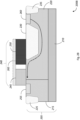
- Fig. 2A is a schematic diagram of a cross-section of the LDMOS 100A, 200A, taken across line l - l , in accordance with various embodiments.
- the sectional view of LDMOS 200A shows the different portions and structures described above, but obscured in the top view.
- LDMOS 200A includes a substrate 205, having an undoped/lightly doped region 210, a first well 215, second well 220, first trench isolation region 225, second trench isolation region 230, third trench isolation region 235, gate 240 having an undoped block 245 and doped block 250, cap 265, source region 255, and drain region 260.
- the various parts and components of LDMOS 200A are schematically illustrated in Fig. 2A , and that modifications to the various components and other arrangements of LDMOS 200A may be possible and in accordance with the various embodiments.
- the substrate 205 may include an undoped/lightly doped region 210 on which the first and second wells 215, 220 are formed.
- the undoped/lightly doped region 210 of the substrate 205 may instead be lightly doped.
- the undoped/lightly doped region 205 is lightly boron doped (e.g., p-type).
- the substrate 205 further includes a first well 215 and second well 220.
- the first and second wells 215, 220 may be heavily doped regions of the substrate 205.
- the first well 215 may be a p-type doped (e.g., boron doped) "p-well," and the second well 220 may be a n-type doped (e.g., phosphorous doped) "n-well.”
- the substrate 205 further includes trench isolation regions, such as first through third trench isolation regions 225-235. Trench isolation regions may be trenches formed in the substrate, and filled with an oxide material.
- one or more of the first, second, and third trench isolation regions 225-235 may be shallow trench isolation (STI) regions.
- one or more of the first, second, and third trench isolation regions 225-235 may be deep trench isolation (DTI) regions.
- STI shallow trench isolation
- DTI deep trench isolation
- the gate 240 may include an undoped block 245 and doped block 250.
- the LDMOS 200A may be an NLDMOS, and a NLDD and/or n + implant may be applied to the doped block 250, giving it one or more of a light n-type doping and heavy n-type doping.
- a PLDMOS a PLDD and/or p + implant may be applied to the doped block 250.
- the doped block 250 may be region of the gate 240 to which NLDD/PLDD and/or n +/ p + implantation is applied, and the undoped block 245 may be a region to which the implant is not applied.
- the undoped and doped block 245, 250 may be part of the structure of the gate 240, and formed as blocks of dielectric material (or parts of the dielectric material forming the gate 240).
- the undoped and doped blocks 245, 250 may be blocks (or regions of a block) of polysilicon forming the gate 240.
- the gate 240 may further include a cap 265.
- the cap 265 may extend over the full gate 240, or partially over the gate 240.
- a partial cap 265 may cover the undoped block 245 and at least part of the doped block 250.
- the cap 265 may, in some examples, be a salicide (e.g., self-aligned silicide) and/or polycide cap 265 that is grown and/or deposited on the gate 240.
- Fig. 2B is a schematic diagram of a cross-section of the LDMOS 100B, 200B, taken across line x-x, in accordance with various embodiments.
- the gate 240 is a split gate in which undoped block 245 is split (e.g., separated) from the doped block 250, forming a split gate.
- a gap is present between the undoped block 245 and doped block 250, the gap being formed over the second well 220.
- the undoped block 245 is disposed at least partially over the source region 255, first well 215, and at least partially over the second well 220.
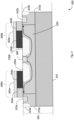
- Fig. 3 is a schematic diagram of a cross-section of an LDMOS portion of a BCDMOS FET 300 (hereinafter "BCDMOS 300"), in accordance with various embodiments.
- the BCDMOS 300 includes a substrate 305, having an undoped/lightly doped region 310, a set of first wells 315a, 315b, a second well 320, a set of first trench isolation regions 325a, 325b, a set of second trench isolation region 330a, 330b, a first gate 340a having a first undoped block 345a and first doped block 350a, first and second caps 365a, 365b, a second gate 340b having a first undoped block 345a and first doped block 350a, a first source region 355a, second source region 355a, and drain region 360.
- the various parts and components of BCDMOS 300 are schematically illustrated in Fig. 3 , and that modifications to the various components and other arrangements of BCDMOS 300
- the BCDMOS 300 may feature a continuous single gate (as opposed to a split gate). However, in contrast with LDMOS 200A, the BCDMOS 300 includes two gates (first gate 340a and second gate 340b). Each gate 340a, 340b includes a respective undoped block 345a, 345b and doped block 350a, 350b.
- the BCDMOS 300 may include two connected LDMOS devices sharing a drain region 360, where the LDMOS devices are flipped in orientation.
- the first LDMOS may have a source-gate-drain configuration (e.g., from left-to-right, a first source region 355a, first gate 340a, followed by the drain region 360).
- the second LDMOS may have a drain-gate-source configuration (e.g., from left-to-right, drain region 360, second gate 340b, followed by the second source region 355b).
- the BCDMOS 300 may include the second well 320 may include two second trench isolation regions 330a, 330b disposed on either side of the drain region 360, separating the drain region 360 from the respective source regions 355a, 355b.
- the gates 340a, 340b may further include respective caps 365a, 365b.
- the first and second caps 365a, 365b may cover an entire respective gate 340a, 340b, or partially cover (e.g., extend partially over) a respective gate 340a, 340b.
- a partial cap 365a, 365b may cover a respective undoped block 345a, 345b and at least part of a respective doped block 350a, 350b.
- the cap 365a, 365b may, in some examples, be a salicide (e.g., self-aligned silicide) and/or polycide that is grown and/or deposited on the respective gate 340a, 340b.
- the second gate 340b includes second undoped block 345b and doped block 350b.
- the second gate 340b may be in a flipped configuration from the first gate 340a, where the second doped block 350b is disposed on the left side, over the second well 320 and second trench isolation region 330b, and doped block 345b is disposed on the right side, disposed on the second well 320, first well 315b, and second source region 355b.
- one or more of the gates 340a, 340b may be a split gate, in which the undoped block 345a, 345b and doped block 350a, 350b are separated, as previously described with respect to Figs. 1B & 2B .
- the gates 340a, 340b may be formed of polysilicon. In each of these configuration, the undoped blocks 345a, 345b of the respective gates 340a, 340b increases the effective thickness of the respective gate 340a, 340b, reducing Qg and HCI induced TDDB.
Landscapes
- Insulated Gate Type Field-Effect Transistor (AREA)
Abstract
An LDMOS with reduced gate charge and time-dependent dielectric breakdown is provided. An apparatus includes a substrate (145, 205, 305) comprising a first well (125, 215, 315) having a first doping and a second well region (130, 220, 320) having a second doping, a source (120, 255, 355) formed in the first well (125, 215, 315), and a gate (105, 240, 340) comprising an undoped block (110, 245, 345) and a doped block (115, 250, 350). The undoped block (110, 245, 345) is disposed at least partially on the source (120, 255, 355), first well (125, 215, 315), and second well (130, 220, 320). The doped block (115, 250, 350) is disposed at least partially on the second well (130, 220, 320).
Description
- A portion of the disclosure of this patent document contains material that is subject to copyright protection. The copyright owner has no objection to the facsimile reproduction by anyone of the patent document or the patent disclosure as it appears in the Patent and Trademark Office patent file or records, but otherwise reserves all copyright rights whatsoever.
- The present disclosure relates, in general, to methods, systems, and apparatuses for gate charge and time-dependent dielectric breakdown reduction in laterally-diffused metal-oxide semiconductor (LDMOS) fin-based field-effect transistors.
- LDMOS field-effect transistors (FET) have been widely adopted as an alternative to complementary metal-oxide semiconductor (CMOS) technology for high voltage applications. The traditional figure of merit (FOM) for LDMOS performance is given as gate charge (Qg) times the drain-source on resistance (RDS(ON)), or Qg * Rns(on). Conventional LDMOS structures exhibit relatively high Qg, and both split gate and conventional gate architectures suffer from hot-carrier injection (HCI) induced TDDB burnout.
- Thus, methods, systems, and apparatuses for a LDMOS architecture with reduced Qg and TDDB are provided.
- A further understanding of the nature and advantages of particular embodiments may be realized by reference to the remaining portions of the specification and the drawings, in which like reference numerals are used to refer to similar components. In some instances, a sub-label is associated with a reference numeral to denote one of multiple similar components. When reference is made to a reference numeral without specification to an existing sub-label, it is intended to refer to all such multiple similar components.
-
Fig. 1A is a schematic top view of a LDMOS FET with reduced Qg and TDDB, in accordance with various embodiments; -
Fig. 1B is a schematic top view of an alternative LDMOS FET with reduced Qg and TDDB, in accordance with various embodiments; -
Fig. 2A is a schematic diagram of a cross-section of the LDMOS FET with reduced Qg and TDDB, in accordance with various embodiments; -
Fig. 2B is a schematic diagram of a cross-section of the alternative LDMOS FET with reduced Qg and TDDB, in accordance with various embodiments; and -
Fig. 3 is a schematic diagram of an LDMOS portion of a bipolar, CMOS, and LDMOS (BCDMOS) FET with reduced Qg and TDDB, in accordance with various embodiments. - Various embodiments set forth a LDMOS device with reduced Qg and TDDB.
- In some embodiments, an apparatus for a LDMOS FET with reduced Qg and TDDB is provided. The apparatus includes a substrate comprising a first well having a first doping and a second well region having a second doping, a source formed in the first well, and a gate comprising an undoped block and a doped block. The undoped block is disposed at least partially on the source, first well, and second well. The doped block is disposed at least partially on the second well.
- In further embodiments, a semiconductor device having an LDMOS FET with reduced Qg and TDDB is provided. The semiconductor device includes a source, a drain, and a gate disposed on a substrate, the gate comprising an undoped region and a doped region. The undoped region disposed at least partially on the source, and the doped region is disposed between the drain and source.
- In further embodiments, an apparatus for an LDMOS with reduced Qg and TDDB is provided. The apparatus includes a substrate comprising a first well having a first doping and a second well region having a second doping, and a gate comprising an undoped block and a doped block, the undoped block disposed at least partially on the first well and the second well, wherein the doped block is disposed at least partially on the second well.
- In the following description, for the purposes of explanation, numerous details are set forth to provide a thorough understanding of the described embodiments. It will be apparent to one skilled in the art, however, that other embodiments may be practiced without some of these details. Several embodiments are described herein, and while various features are ascribed to different embodiments, it should be appreciated that the features described with respect to one embodiment may be incorporated with other embodiments as well. By the same token, however, no single feature or features of any described embodiment should be considered essential to every embodiment of the invention, as other embodiments of the invention may omit such features.
- When an element is referred to herein as being "connected" or "coupled" to another element, it is to be understood that the elements can be directly connected to the other element, or have intervening elements present between the elements. In contrast, when an element is referred to as being "directly connected" or "directly coupled" to another element, it should be understood that no intervening elements are present in the "direct" connection between the elements. However, the existence of a direct connection does not exclude other connections, in which intervening elements may be present.
- When an element is referred to herein as being "disposed" in some manner relative to another element (e.g., disposed on, disposed between, disposed under, disposed adjacent to, or disposed in some other relative manner), it is to be understood that the elements can be directly disposed relative to the other element (e.g., disposed directly on another element), or have intervening elements present between the elements. In contrast, when an element is referred to as being "disposed directly" relative to another element, it should be understood that no intervening elements are present in the "direct" example. However, the existence of a direct disposition does not exclude other examples in which intervening elements may be present.
- Likewise, when an element is referred to herein as being a "layer," it is to be understood that the layer can be a single layer or include multiple layers. For example, a conductive layer may comprise multiple different conductive materials or multiple layers of different conductive materials, and a dielectric layer may comprise multiple dielectric materials or multiple layers of dielectric materials. When a layer is described as being coupled or connected to another layer, it is to be understood that the coupled or connected layers may include intervening elements present between the coupled or connected layers. In contrast, when a layer is referred to as being "directly" connected or coupled to another layer, it should be understood that no intervening elements are present between the layers. However, the existence of directly coupled or connected layers does not exclude other connections in which intervening elements may be present.
- Moreover, the terms left, right, front, back, top, bottom, forward, reverse, clockwise and counterclockwise are used for purposes of explanation only and are not limited to any fixed direction or orientation. Rather, they are used merely to indicate relative locations and/or directions between various parts of an object and/or components.
- Furthermore, the methods and processes described herein may be described in a particular order for ease of description. However, it should be understood that, unless the context dictates otherwise, intervening processes may take place before and/or after any portion of the described process, and further various procedures may be reordered, added, and/or omitted in accordance with various embodiments.
- Unless otherwise indicated, all numbers used herein to express quantities, dimensions, and so forth should be understood as being modified in all instances by the term "about." In this application, the use of the singular includes the plural unless specifically stated otherwise, and use of the terms "and" and "or" means "and/or" unless otherwise indicated. Moreover, the use of the terms "including" and "having," as well as other forms, such as "includes," "included," "has," "have," and "had," should be considered non-exclusive. Also, terms such as "element" or "component" encompass both elements and components comprising one unit and elements and components that comprise more than one unit, unless specifically stated otherwise.
- As used herein, the phrase "at least one of" preceding a series of items, with the term "and" or "or" to separate any of the items, modifies the list as a whole, rather than each member of the list (i.e., each item). The phrase "at least one of" does not require selection of at least one of each item listed; rather, the phrase allows a meaning that includes at least one of any one of the items, and/or at least one of any combination of the items. By way of example, the phrases "at least one of A, B, and C" or "at least one of A, B, or C" each refer to only A, only B, or only C; and/or any combination of A, B, and C. In instances where it is intended that a selection be of "at least one of each of A, B, and C," or alternatively, "at least one of A, at least one of B, and at least one of C," it is expressly described as such.
- The FOM for LDMOS has traditionally been given as Qg * RDS(ON). Conventional approaches to improving the FOM exhibit high Qg. These may include drain extensions, surface implant processes, and split gate architectures. These approaches exhibit a high Qg. Moreover, when under HCI stress, TDDB and burnout have occurred in these designs.
- In some embodiments, a proposed LDMOS architecture provides a reduced Qg and TDDB, including split gate architectures. By providing a region of gate polysilicon that does not receive heaving doping (e.g., n+ for heavy n-type doping, or p+ for heavy p-type doping) and does not receive a respective lightly-doped drain (LDD) implant (e.g., NLDD for n-type LDD, or PLDD for p-type LDD), the effective thickness of the gate oxide increases due to the polysilicon depletion effect. This in turn reduces Qg, and further reduces vertical electric field (which reduced TDDB). As a result, gate leakage current is reduced.
-
Fig. 1A is a schematic top view of aLDMOS FET 100A (hereinafter "LDMOS 100A") with reduced Qg and TDDB, in accordance with various embodiments. TheLDMOS 100A includes agate 105 having anundoped block 110 and dopedblock 115,source region 120, afirst well 125, second well 130,trench isolation region 135, and drainregion 140, andsubstrate 145. It should be noted that the various parts and components ofLDMOS 100A are schematically illustrated inFig. 1A , and that modifications to the various components and other arrangements ofLDMOS 100A may be possible and in accordance with the various embodiments. - In various embodiments, the structures of the
LDMOS 100A are disposed on thesubstrate 145. Accordingly, thesubstrate 145 may be a semiconductor substrate, such as, without limitation, bulk silicon. In some embodiments, thesubstrate 145 includes a lightly doped ("p-" or "n-") region. For example, in the case of an n-type LDMOS (NLDMOS), thesubstrate 145 may be lightly boron doped (e.g., p-), in which well regions may be formed (e.g., p-well and n-well). A well, accordingly, refers to a doped region formed within thesubstrate 145, which serves as the "bulk" or "body" of theLDMOS 100A, on (or in) which other parts of the device are formed, such as thegate 105,source region 120,trench isolation region 135, and drainregion 140. - In the embodiments above, and further embodiments set forth below, boron and phosphorous are provided as non-limiting examples, and it is to be understood that in other embodiments, other dopants may be utilized. For example, suitable dopants may include, without limitation, pentavalent atoms (e.g., arsenic, phosphorous, antimony, bismuth, lithium, etc.) for n-type doping and trivalent atoms (e.g., indium, aluminum, gallium, boron, etc.) for p-type doping.
- In various embodiments, the
source region 120, first well 125, second well 130,trench isolation region 135, and drainregion 140 may be formed within thesubstrate 145. Specifically, as will be discussed in greater detail below with respect toFigs. 2A ,2B &3 , thesource region 120, first well 125, second well 130,trench isolation region 135, and drainregion 140 may be formed via doping of different regions of thesubstrate 145. - In some embodiments, the
substrate 145 may include one or more heavily doped ("p+" or "n+") regions, respectively doped with n-type (e.g., phosphorous) and p-type dopants (e.g., boron). In some examples, n+ or p+ regions may include thesource region 120 and/or drainregion 140. Other doped regions of thesubstrate 145 include afirst well 125 having a first doping and second well 130 having a second doping different from the first. In some examples, theLDMOS 100A may be an NLDMOS. Accordingly, the first well 125 may have a p-type doping (e.g., a p-well), and the second well 130 may have a n-type doping (e.g., a n-well). Moreover, in an NLDMOS, the source and drainregions substrate 145. - In various examples, the
gate 105 is disposed on thesubstrate 145, over at least part of thesource region 120, thefirst well 125, second well 130, andtrench isolation region 135. In various examples, thegate 105 may be formed via an epitaxial process in which the gate may be grown or otherwise deposited on thesubstrate 145. Accordingly, in some examples, thegate 105 may be a polysilicon (e.g., polycrystalline silicon) gate, formed of a polysilicon material. In other examples, thegate 105 may be a partially- or fully-silicided poly silicon gate (as will be described in greater detail below with respect toFigs. 2A ,2B , &3 . - In various embodiments, the
gate 105 includes anundoped block 110 and adoped block 115. As used herein, the term "block" refers to a piece of gate material (e.g., polysilicon, metal oxide, or other gate dielectric material) forming the structure gate, and/or a region of thegate 105. In some examples, thedoped block 115 of thegate 105 may be doped via ion implantation. In some embodiments, thedoped block 115 may have a LDD and/or heavy doping (e.g., n+, p+) implant applied, thereby receiving both a light doping and heavy doping. In some examples, the implant is an NLDD / n+ implant, thedoped block 115 thereby receiving a light n-type doping and/or a heavy n-type (n+) doping. Accordingly, as used herein, "implant" refers to the process of doping via ion implantation into a respective structure. Thus, in some examples, thedoped block 115 may receive both NLDD and n+ doping, forming a doped portion of thegate 105. - In various embodiments, the
gate 105 further includes anundoped bloc k 110 which does not receive doping. For example, in some embodiments, an n+ and NLDD implant (or other implant) may not be applied to theundoped block 110 of thegate 105, thereby forming an undoped portion of thegate 105. An implant, as used herein, refers to a process of doping via masking and ion implantation into a structure, such as thedoped block 115 ofgate 105. - Thus, the
gate 105 includes both anundoped portion 110 and dopedportion 115. Theundoped portion 110 of thegate 105 extends the effective thickness of the gate oxide due to the polysilicon depletion effect. In turn, Qg is reduced, and vertical electric fields are also reduced (which in turn mitigates TDDB). As a result, gate leakage current is also reduced. - In various embodiments, the
source region 120 may be formed within thesubstrate 145, and disposed at least partially under theundoped block 110, and at least partially to the left side of theundoped block 110. Thefirst well 125 is disposed directly adjacent to thesource region 120 on a right side of thesource region 120, and under theundoped block 110. Thesecond well 130 is disposed directly adjacent to the first well 125 on a right side of thefirst well 125. Thesecond well 130 is further disposed, at least partially, under theundoped block 110 and dopedblock 115 of thegate 105. In some examples, the second well 130 may be disposed under thedoped block 115, but not theundoped block 110. In other words, thedoped block 115 may be disposed on the second well 125 up to the border between thefirst well 125 andsecond well 130. Theundoped block 110, in turn, may be disposed, at least partially, on thefirst well 125, but not thesecond well 130. In some examples, thetrench isolation region 135 may be disposed directly adjacent to thesecond well 130, on a right side of thesecond well 130. Thetrench isolation region 135 may be disposed, at least partially, under the doped region of the gate (e.g., doped block 115). Thedrain region 140 may be disposed directly adjacent to thetrench isolation region 135, on a right side of thetrench isolation region 135. - Accordingly, in some embodiments, the
source region 120 may be a heavily doped (e.g., n-type heavily doped (n+) or p-type heavily doped (p+)) region within the substrate, disposed on a first side of theundoped block 110 of thegate 105, and at least partially under the undoped region of the gate (e.g., undoped block 110). Thesource region 120 may, in some examples, be referred to interchangeably as the "source" or "source/drain" of theLDMOS 100A. In some further embodiments, thesource region 120 may be formed as raised source / drain (RSD) structures. In some further embodiments, thesource region 120 may be part of a fin (e.g., as in a FinFET device). - Similarly, the
drain region 140 may be a heavily doped (e.g., n+ or p+) region within the substrate, disposed on a second side, opposite the first, (e.g., a right side of the doped block 115) of thegate 105. Thedrain region 140 may, in some examples, be referred to interchangeably as the "drain" or "drain/source" of theLDMOS 100A. In some further embodiments, thedrain region 140, likesource region 120, may be formed as raised source / drain (RSD) structures. In some further embodiments, the source region may be part of a fin (e.g., as in a FinFET device). The fin may be heavily doped, and formed as part of the drain (also referred to as "drain/source"). - In various examples, the
substrate 145 further includes trench isolation regions, such as thetrench isolation regions 135. Trench isolation regions may be trenches formed in the substrate, and filled with an oxide material. In some examples, thetrench isolation region 135 may be a shallow trench isolation (STI) region. In other examples, thetrench isolation region 135 may be a deep trench isolation (DTI) region. Trench isolation regions are filled trench regions configured to mitigate leakage current between different components, in this example, electric field and/or leakage current between the source and drainregions undoped block 110 of thegate 105, and corresponding increase in effective thickness of thegate 105, reduces the effects of HCI induced TDDB. -
Fig. 1B is a schematic top view of an alternative configuration for anLDMOS FET 100B (hereinafter "LDMOS 100B") with reduced Qg and TDDB, in accordance with various embodiments. TheLDMOS 100B includes agate 105 having anundoped block 110 and dopedblock 115,source region 120, afirst well 125, second well 130,trench isolation region 135, and drainregion 140, andsubstrate 145. It should be noted that the various parts and components ofLDMOS 100B are schematically illustrated inFig. 1B , and that modifications to the various components and other arrangements ofLDMOS 100B may be possible and in accordance with the various embodiments. - In contrast with
LDMOS 100A ofFig. 1A , thegate 105 ofLDMOS 100B is a split gate architecture, in which the structure of the gate is "split" into two separate gate structures (e.g., gate structures that are spaced apart on the surface of thesubstrate 145 and not in direct contact), as opposed to a single gate FET as shown inLDMOS 100A. In the embodiments depicted, theundoped block 110 is split (e.g., separated) from the dopedblock 115, forming a split gate. Accordingly, in some embodiments, a gap is present between theundoped block 110 and dopedblock 115, separating the undoped and dopedblocks second well 130. Specifically, theundoped block 110 is disposed at least partially over thesource region 120, first well 125, and at least partially over thesecond well 130. -
Fig. 2A is a schematic diagram of a cross-section of theLDMOS LDMOS 200A shows the different portions and structures described above, but obscured in the top view. Accordingly,LDMOS 200A includes asubstrate 205, having an undoped/lightly dopedregion 210, afirst well 215, second well 220, firsttrench isolation region 225, secondtrench isolation region 230, thirdtrench isolation region 235,gate 240 having anundoped block 245 and dopedblock 250,cap 265,source region 255, and drainregion 260. It should be noted that the various parts and components ofLDMOS 200A are schematically illustrated inFig. 2A , and that modifications to the various components and other arrangements ofLDMOS 200A may be possible and in accordance with the various embodiments. - As shown in the cross-sectional view, the
substrate 205 may include an undoped/lightly dopedregion 210 on which the first andsecond wells region 210 of thesubstrate 205 may instead be lightly doped. For example, in an NLDMOS, the undoped/lightly dopedregion 205 is lightly boron doped (e.g., p-type). In various examples, thesubstrate 205 further includes afirst well 215 andsecond well 220. In various examples, the first andsecond wells substrate 205. For example, in an NLDMOS, the first well 215 may be a p-type doped (e.g., boron doped) "p-well," and the second well 220 may be a n-type doped (e.g., phosphorous doped) "n-well." In various examples, thesubstrate 205 further includes trench isolation regions, such as first through third trench isolation regions 225-235. Trench isolation regions may be trenches formed in the substrate, and filled with an oxide material. In some examples, one or more of the first, second, and third trench isolation regions 225-235 may be shallow trench isolation (STI) regions. In some examples, one or more of the first, second, and third trench isolation regions 225-235 may be deep trench isolation (DTI) regions. - As previously described with respect to
Fig. 1A , thegate 240 may include anundoped block 245 and dopedblock 250. In some embodiments, theLDMOS 200A may be an NLDMOS, and a NLDD and/or n+ implant may be applied to thedoped block 250, giving it one or more of a light n-type doping and heavy n-type doping. In other embodiments, such as a PLDMOS, a PLDD and/or p+ implant may be applied to thedoped block 250. Accordingly, thedoped block 250 may be region of thegate 240 to which NLDD/PLDD and/or n+/p+ implantation is applied, and theundoped block 245 may be a region to which the implant is not applied. As previously described, the undoped anddoped block gate 240, and formed as blocks of dielectric material (or parts of the dielectric material forming the gate 240). In some examples, the undoped and dopedblocks gate 240. - Accordingly, in various examples, the
gate 240 may further include acap 265. Thecap 265 may extend over thefull gate 240, or partially over thegate 240. In some examples, apartial cap 265 may cover theundoped block 245 and at least part of the dopedblock 250. Thecap 265 may, in some examples, be a salicide (e.g., self-aligned silicide) and/orpolycide cap 265 that is grown and/or deposited on thegate 240. -
Fig. 2B is a schematic diagram of a cross-section of theLDMOS Fig. 1B , in contrast withLDMOS 200A, in the examples depicted, thegate 240 is a split gate in whichundoped block 245 is split (e.g., separated) from the dopedblock 250, forming a split gate. Accordingly, in some embodiments, a gap is present between theundoped block 245 and dopedblock 250, the gap being formed over thesecond well 220. Specifically, theundoped block 245 is disposed at least partially over thesource region 255, first well 215, and at least partially over thesecond well 220. -
Fig. 3 is a schematic diagram of a cross-section of an LDMOS portion of a BCDMOS FET 300 (hereinafter "BCDMOS 300"), in accordance with various embodiments. TheBCDMOS 300 includes a substrate 305, having an undoped/lightly dopedregion 310, a set offirst wells 315a, 315b, asecond well 320, a set of firsttrench isolation regions trench isolation region first gate 340a having a firstundoped block 345a and firstdoped block 350a, first andsecond caps second gate 340b having a firstundoped block 345a and firstdoped block 350a, afirst source region 355a,second source region 355a, and drainregion 360. It should be noted that the various parts and components ofBCDMOS 300 are schematically illustrated inFig. 3 , and that modifications to the various components and other arrangements ofBCDMOS 300 may be possible and in accordance with the various embodiments - Like the
LDMOS 200A, theBCDMOS 300 may feature a continuous single gate (as opposed to a split gate). However, in contrast withLDMOS 200A, theBCDMOS 300 includes two gates (first gate 340a andsecond gate 340b). Eachgate undoped block block BCDMOS 300 may include two connected LDMOS devices sharing adrain region 360, where the LDMOS devices are flipped in orientation. For example, the first LDMOS may have a source-gate-drain configuration (e.g., from left-to-right, afirst source region 355a,first gate 340a, followed by the drain region 360). The second LDMOS may have a drain-gate-source configuration (e.g., from left-to-right, drainregion 360,second gate 340b, followed by thesecond source region 355b). Furthermore, theBCDMOS 300 may include the second well 320 may include two secondtrench isolation regions drain region 360, separating thedrain region 360 from therespective source regions - In various examples, the
gates respective caps second caps respective gate respective gate partial cap undoped block block cap respective gate - As depicted, the
second gate 340b includes secondundoped block 345b and dopedblock 350b. Thesecond gate 340b may be in a flipped configuration from thefirst gate 340a, where the seconddoped block 350b is disposed on the left side, over thesecond well 320 and secondtrench isolation region 330b, and dopedblock 345b is disposed on the right side, disposed on thesecond well 320,first well 315b, andsecond source region 355b. - It is to be understood that in other embodiments, other gate configurations may be utilized. For example, in some embodiments, one or more of the
gates undoped block block Figs. 1B &2B . As previously described, in various embodiments, thegates undoped blocks respective gates respective gate - While some features and aspects have been described with respect to the embodiments, one skilled in the art will recognize that numerous modifications are possible. For example, the methods and processes described herein may be implemented using hardware components, custom integrated circuits (ICs), programmable logic, and/or any combination thereof. Further, while various methods and processes described herein may be described with respect to particular structural and/or functional components for ease of description, methods provided by various embodiments are not limited to any particular structural and/or functional architecture but instead can be implemented in any suitable hardware configuration. Similarly, while some functionality is ascribed to one or more system components, unless the context dictates otherwise, this functionality can be distributed among various other system components in accordance with the several embodiments.
- Moreover, while the procedures of the methods and processes described herein are described in a particular order for ease of description, unless the context dictates otherwise, various procedures may be reordered, added, and/or omitted in accordance with various embodiments. Moreover, the procedures described with respect to one method or process may be incorporated within other described methods or processes; likewise, system components described according to a particular structural architecture and/or with respect to one system may be organized in alternative structural architectures and/or incorporated within other described systems. Hence, while various embodiments are described with or without some features for ease of description and to illustrate aspects of those embodiments, the various components and/or features described herein with respect to a particular embodiment can be substituted, added and/or subtracted from among other described embodiments, unless the context dictates otherwise. Consequently, although several embodiments are described above, it will be appreciated that the invention is intended to cover all modifications and equivalents within the scope of the following claims.
Claims (15)
- An apparatus comprising:a substrate (145, 205, 305) comprising a first well (125, 215, 315) having a first doping and a second well region (130, 220, 320) having a second doping;a source (120, 255, 355) formed in the first well (125, 215, 315); anda gate (105, 240, 340) comprising an undoped block (110, 245, 345) and a doped block (115, 250, 350), the undoped block (110, 245, 345) disposed at least partially on the source (120, 255, 355), first well (125, 215, 315), and second well (130, 220, 320), wherein the doped block (115, 250, 350) is disposed at least partially on the second well (130, 220, 320).
- The apparatus of claim 1, wherein the gate (105, 240, 340) is a split gate, wherein the doped block (115, 250, 350) and undoped block (110, 245, 345) are separated.
- The apparatus of claim 1 or 2, comprising at least one of the following features:wherein the gate (105, 240, 340) is formed of polycrystalline silicon;wherein the first doping is a p-type doping, and the second doping is an n-type doping;wherein the source (120, 255, 355) is a heavily n-type doped region in the first well (125, 215, 315).
- The apparatus of any of claims 1 to 3, wherein the doped block (115, 250, 350) has at least one of a light doping implant or heavy doping implant applied.
- The apparatus of claim 4, comprising at least one of the following features:wherein the doped block (115, 250, 350) has an n-type lightly doped drain implant and n-type heavy doping implant applied;wherein the implant includes a light and heavy doping of a same type as the second doping.
- The apparatus of any of claims 1 to 5, wherein the substrate (145, 205, 305) includes a shallow trench isolation region (135, 225, 230, 235, 325) formed in the second well (130, 220, 320), wherein the shallow trench isolation region (135, 225, 230, 235, 325) is disposed between a drain formed in the second well (130, 220, 320) and the source (120, 255, 355), wherein the doped block (115, 250, 350) is disposed at least partially on the shallow trench isolation region (135, 225, 230, 235, 325).
- A semiconductor device comprising:a source (120, 255, 355);a drain (140, 260, 360); anda gate (105, 240, 340) disposed on a substrate (145, 205, 305), the gate (105, 240, 340) comprising an undoped region and a doped region, the undoped region disposed at least partially on the source (120, 255, 355), wherein the doped region is disposed between the drain (140, 260, 360) and source (120, 255, 355).
- The apparatus of claim 7, comprising at least one of the following features:wherein the gate (105, 240, 340) is a split gate, wherein the doped region and undoped regions are separate respective blocks of dielectric material;wherein the gate (105, 240, 340) is formed of polycrystalline silicon.
- The apparatus of claim 7 or 8, wherein the doped block (115, 250, 350) has at least one of a light doping implant or heavy doping implant applied.
- The apparatus of claim 9, wherein the doped block (115, 250, 350) has an n-type lightly doped drain implant and n-type heavy doping implant applied.
- The apparatus of any of claims 7 to 10, wherein the substrate (145, 205, 305) includes a shallow trench isolation region (135, 225, 230, 235, 325) disposed between the drain (140, 260, 360) and source (120, 255, 355), wherein the doped block (115, 250, 350) is disposed at least partially on the shallow trench isolation region (135, 225, 230, 235, 325).
- An apparatus comprising:a substrate (145, 205, 305) comprising a first well (125, 215, 315) having a first doping and a second well region (130, 220, 320) having a second doping; anda gate (105, 240, 340) comprising an undoped block (110, 245, 345) and a doped block (115, 250, 350), the undoped block (110, 245, 345) disposed at least partially on the first well (125, 215, 315) and the second well (130, 220, 320), wherein the doped block (115, 250, 350) is disposed at least partially on the second well (130, 220, 320).
- The substrate (145, 205, 305) of claim 12, comprising at least one of the following features:wherein the gate (105, 240, 340) is a split gate, wherein the doped block (115, 250, 350) and undoped block (110, 245, 345) are separated blocks of dielectric material;wherein the gate (105, 240, 340) is formed of polycrystalline silicon.
- The substrate (145, 205, 305) of claim 12 or 13, wherein the first doping is a p-type doping, and the second doping is an n-type doping.
- The substrate (145, 205, 305) of claim 14, wherein the doped block (115, 250, 350) has at least one of an n-type lightly doped drain implant and an n-type heavy doping implant applied.
Applications Claiming Priority (1)
| Application Number | Priority Date | Filing Date | Title |
|---|---|---|---|
| US18/361,834 US20250040178A1 (en) | 2023-07-29 | 2023-07-29 | Laterally-Diffused Metal-Oxide Semiconductor Devices with Reduced Gate Charge and Time-Dependent Dielectric Breakdown |
Publications (1)
| Publication Number | Publication Date |
|---|---|
| EP4503135A1 true EP4503135A1 (en) | 2025-02-05 |
Family
ID=92042859
Family Applications (1)
| Application Number | Title | Priority Date | Filing Date |
|---|---|---|---|
| EP24190983.7A Pending EP4503135A1 (en) | 2023-07-29 | 2024-07-25 | Laterally-diffused metal-oxide semiconductor devices with reduced gate charge and time-dependent dielectric breakdown |
Country Status (3)
| Country | Link |
|---|---|
| US (1) | US20250040178A1 (en) |
| EP (1) | EP4503135A1 (en) |
| CN (1) | CN119451172A (en) |
Citations (3)
| Publication number | Priority date | Publication date | Assignee | Title |
|---|---|---|---|---|
| JPH06275821A (en) * | 1993-03-18 | 1994-09-30 | Seiko Instr Inc | Mos transistor and its manufacture |
| US20100230748A1 (en) * | 2009-03-12 | 2010-09-16 | Sharp Kabushiki Kaisha | Semiconductor device and method of manufacturing the same |
| US20150263167A1 (en) * | 2014-03-11 | 2015-09-17 | Kabushiki Kaisha Toshiba | Multigate dual work function device and method for manufacturing same |
Family Cites Families (6)
| Publication number | Priority date | Publication date | Assignee | Title |
|---|---|---|---|---|
| DE69125794T2 (en) * | 1990-11-23 | 1997-11-27 | Texas Instruments Inc | Method for simultaneously producing an insulated gate field effect transistor and a bipolar transistor |
| US7301185B2 (en) * | 2004-11-29 | 2007-11-27 | Taiwan Semiconductor Manufacturing Company, Ltd. | High-voltage transistor device having an interlayer dielectric etch stop layer for preventing leakage and improving breakdown voltage |
| US8748271B2 (en) * | 2011-03-11 | 2014-06-10 | Globalfoundries Singapore Pte. Ltd. | LDMOS with improved breakdown voltage |
| US9490360B2 (en) * | 2014-02-19 | 2016-11-08 | United Microelectronics Corp. | Semiconductor device and operating method thereof |
| US9859415B2 (en) * | 2015-09-17 | 2018-01-02 | Globalfoundries Singapore Pte. Ltd. | High voltage transistor |
| CN105304500B (en) * | 2015-10-26 | 2018-01-30 | 深圳市华星光电技术有限公司 | N-type TFT preparation method |
-
2023
- 2023-07-29 US US18/361,834 patent/US20250040178A1/en active Pending
-
2024
- 2024-05-29 CN CN202410678571.4A patent/CN119451172A/en active Pending
- 2024-07-25 EP EP24190983.7A patent/EP4503135A1/en active Pending
Patent Citations (3)
| Publication number | Priority date | Publication date | Assignee | Title |
|---|---|---|---|---|
| JPH06275821A (en) * | 1993-03-18 | 1994-09-30 | Seiko Instr Inc | Mos transistor and its manufacture |
| US20100230748A1 (en) * | 2009-03-12 | 2010-09-16 | Sharp Kabushiki Kaisha | Semiconductor device and method of manufacturing the same |
| US20150263167A1 (en) * | 2014-03-11 | 2015-09-17 | Kabushiki Kaisha Toshiba | Multigate dual work function device and method for manufacturing same |
Also Published As
| Publication number | Publication date |
|---|---|
| US20250040178A1 (en) | 2025-01-30 |
| CN119451172A (en) | 2025-02-14 |
Similar Documents
| Publication | Publication Date | Title |
|---|---|---|
| US9159803B2 (en) | Semiconductor device with HCI protection region | |
| US10170589B2 (en) | Vertical power MOSFET and methods for forming the same | |
| US9184283B2 (en) | High voltage device | |
| US8461647B2 (en) | Semiconductor device having multi-thickness gate dielectric | |
| US8664718B2 (en) | Power MOSFETs and methods for forming the same | |
| US9059275B2 (en) | Semiconductor device | |
| US8748271B2 (en) | LDMOS with improved breakdown voltage | |
| US9741793B2 (en) | Semiconductor device with false drain | |
| US11069804B2 (en) | Integration of HVLDMOS with shared isolation region | |
| US11769812B2 (en) | Semiconductor device having multiple wells and method of making | |
| US9728600B2 (en) | Partially biased isolation in semiconductor devices | |
| EP3142150B1 (en) | Partially biased isolation in semiconductor devices | |
| CN103762177A (en) | Reduction of proximity effects in field-effect transistors with embedded silicon-germanium source and drain regions | |
| US6635925B1 (en) | Semiconductor device and method of manufacturing the same | |
| CN108574014A (en) | LDMOS device and its manufacturing method | |
| US20250040178A1 (en) | Laterally-Diffused Metal-Oxide Semiconductor Devices with Reduced Gate Charge and Time-Dependent Dielectric Breakdown | |
| US8643104B1 (en) | Lateral diffusion metal oxide semiconductor transistor structure | |
| US20230061138A1 (en) | Semiconductor device structure and method of forming the same | |
| US12513941B2 (en) | Semiconductor device and method for forming the same | |
| US20130099327A1 (en) | Cmos devices and method for manufacturing the same | |
| US9543303B1 (en) | Complementary metal oxide semiconductor device with dual-well and manufacturing method thereof | |
| EP3731281B1 (en) | Lateral semiconductor device having raised source and drain, and method of manufacture thererof | |
| CN1983633B (en) | High voltage semiconductor component and manufacturing method thereof | |
| EP3742498A1 (en) | Semiconductor device structure | |
| US20220085184A1 (en) | Semiconductor device |
Legal Events
| Date | Code | Title | Description |
|---|---|---|---|
| PUAI | Public reference made under article 153(3) epc to a published international application that has entered the european phase |
Free format text: ORIGINAL CODE: 0009012 |
|
| STAA | Information on the status of an ep patent application or granted ep patent |
Free format text: STATUS: THE APPLICATION HAS BEEN PUBLISHED |
|
| AK | Designated contracting states |
Kind code of ref document: A1 Designated state(s): AL AT BE BG CH CY CZ DE DK EE ES FI FR GB GR HR HU IE IS IT LI LT LU LV MC ME MK MT NL NO PL PT RO RS SE SI SK SM TR |
|
| STAA | Information on the status of an ep patent application or granted ep patent |
Free format text: STATUS: REQUEST FOR EXAMINATION WAS MADE |
|
| 17P | Request for examination filed |
Effective date: 20250801 |