EP4503033A1 - A high density 3d magnetic memory device - Google Patents
A high density 3d magnetic memory device Download PDFInfo
- Publication number
- EP4503033A1 EP4503033A1 EP23189234.0A EP23189234A EP4503033A1 EP 4503033 A1 EP4503033 A1 EP 4503033A1 EP 23189234 A EP23189234 A EP 23189234A EP 4503033 A1 EP4503033 A1 EP 4503033A1
- Authority
- EP
- European Patent Office
- Prior art keywords
- magnetic
- memory device
- stack
- material channel
- metallic layer
- Prior art date
- Legal status (The legal status is an assumption and is not a legal conclusion. Google has not performed a legal analysis and makes no representation as to the accuracy of the status listed.)
- Granted
Links
Images





Classifications
-
- H—ELECTRICITY
- H10—SEMICONDUCTOR DEVICES; ELECTRIC SOLID-STATE DEVICES NOT OTHERWISE PROVIDED FOR
- H10B—ELECTRONIC MEMORY DEVICES
- H10B61/00—Magnetic memory devices, e.g. magnetoresistive RAM [MRAM] devices
-
- G—PHYSICS
- G11—INFORMATION STORAGE
- G11C—STATIC STORES
- G11C11/00—Digital stores characterised by the use of particular electric or magnetic storage elements; Storage elements therefor
- G11C11/02—Digital stores characterised by the use of particular electric or magnetic storage elements; Storage elements therefor using magnetic elements
- G11C11/16—Digital stores characterised by the use of particular electric or magnetic storage elements; Storage elements therefor using magnetic elements using elements in which the storage effect is based on magnetic spin effect
- G11C11/161—Digital stores characterised by the use of particular electric or magnetic storage elements; Storage elements therefor using magnetic elements using elements in which the storage effect is based on magnetic spin effect details concerning the memory cell structure, e.g. the layers of the ferromagnetic memory cell
-
- G—PHYSICS
- G11—INFORMATION STORAGE
- G11C—STATIC STORES
- G11C11/00—Digital stores characterised by the use of particular electric or magnetic storage elements; Storage elements therefor
- G11C11/02—Digital stores characterised by the use of particular electric or magnetic storage elements; Storage elements therefor using magnetic elements
- G11C11/16—Digital stores characterised by the use of particular electric or magnetic storage elements; Storage elements therefor using magnetic elements using elements in which the storage effect is based on magnetic spin effect
- G11C11/165—Auxiliary circuits
- G11C11/1659—Cell access
-
- G—PHYSICS
- G11—INFORMATION STORAGE
- G11C—STATIC STORES
- G11C11/00—Digital stores characterised by the use of particular electric or magnetic storage elements; Storage elements therefor
- G11C11/02—Digital stores characterised by the use of particular electric or magnetic storage elements; Storage elements therefor using magnetic elements
- G11C11/16—Digital stores characterised by the use of particular electric or magnetic storage elements; Storage elements therefor using magnetic elements using elements in which the storage effect is based on magnetic spin effect
- G11C11/165—Auxiliary circuits
- G11C11/1673—Reading or sensing circuits or methods
-
- G—PHYSICS
- G11—INFORMATION STORAGE
- G11C—STATIC STORES
- G11C11/00—Digital stores characterised by the use of particular electric or magnetic storage elements; Storage elements therefor
- G11C11/02—Digital stores characterised by the use of particular electric or magnetic storage elements; Storage elements therefor using magnetic elements
- G11C11/16—Digital stores characterised by the use of particular electric or magnetic storage elements; Storage elements therefor using magnetic elements using elements in which the storage effect is based on magnetic spin effect
- G11C11/165—Auxiliary circuits
- G11C11/1675—Writing or programming circuits or methods
-
- G—PHYSICS
- G11—INFORMATION STORAGE
- G11C—STATIC STORES
- G11C11/00—Digital stores characterised by the use of particular electric or magnetic storage elements; Storage elements therefor
- G11C11/18—Digital stores characterised by the use of particular electric or magnetic storage elements; Storage elements therefor using Hall-effect devices
-
- G—PHYSICS
- G11—INFORMATION STORAGE
- G11C—STATIC STORES
- G11C19/00—Digital stores in which the information is moved stepwise, e.g. shift registers
- G11C19/02—Digital stores in which the information is moved stepwise, e.g. shift registers using magnetic elements
- G11C19/08—Digital stores in which the information is moved stepwise, e.g. shift registers using magnetic elements using thin films in plane structure
- G11C19/0808—Digital stores in which the information is moved stepwise, e.g. shift registers using magnetic elements using thin films in plane structure using magnetic domain propagation
- G11C19/0841—Digital stores in which the information is moved stepwise, e.g. shift registers using magnetic elements using thin films in plane structure using magnetic domain propagation using electric current
Definitions
- the present disclosure relates to magnetic memory devices.
- the present disclosure presents a new kind of magnetic memory device that may achieve a high memory density (bit density).
- the magnetic memory device of this disclosure is based on a spin orbit torque (SOT) magnetic random access memory (MRAM) device architecture.
- SOT spin orbit torque
- MRAM magnetic random access memory
- SRAM static random access memory
- DRAM Dynamic random access memory
- SSDs solid state drives
- a first aspect of this disclosure provides a 3D magnetic memory device, the magnetic memory device comprising: a stack comprising a plurality of dielectric layers and silicon-based layers, which are alternatingly arranged one on the other; magnetic material channel formed through the stack, wherein the magnetic material channel extends through each layer of the stack, wherein the magnetic material channel has a first diameter where it extends through a silicon-based layer and a second diameter where it extends through a dielectric layer of the stack, and wherein a plurality of pinning sites defined by the plurality of layers of the stack is formed in the magnetic material channel, each pinning site being configured to store one magnetic bit; a first metallic layer arranged on a first end of the magnetic material channel and on the last layer of the stack; a magnetic tunnel junction, MTJ, arranged on the first metallic layer; and a first electrode arranged on the first metallic layer at a distance to the MTJ; wherein either the first metallic layer is configured as a spin-orbit-torque, SOT, track, or the
- the dielectric layers are silicon oxide layers and the silicon-based layers are silicon nitride layers; or the dielectric layers are silicon layers and the silicon-based layers are silicon germanium layers.
- the MTJ 14 may be arranged directly above the first end of the magnetic material channel 12 on the first metallic layer 13.
- FIG. 2 shows another example of a 3D magnetic memory device 10 according to this disclosure. Same elements of the memory devices 10 in FIG. 1 and FIG. 2 share the same reference signs.
- the first metallic layer 13 may be configured as a SOT track. That is, the first metallic layer 13 may be made of a certain material, have a certain thickness, and may be connected to suitable electrodes, to allow passing an SOT current I SOT through the layer 13, which causes a magnetic bit to be written by SOT into the pinning site defined by the layer of the stack 11 that is closest to the first metallic layer 13.
- the magnetic memory device 10 may comprise a second electrode 41 (Also referred to as ⁇ bottom electrode'), which is arranged on or directly below a second end of the magnetic material channel 12.
- the second electrode 41 may be placed on the second metallic layer 16, as shown.
- the second electrode 41 could be placed directly on the second end of the magnetic material channel 12 and the first layer of the stack 11.
- the second electrode 41 may allow sending a push current I Push into the magnetic material channel 12 and towards the first electrode 15.
- the magnetic memory device 10 may comprise a further first electrode 51 (also referred to as ⁇ further top electrode'). Further, the magnetic memory device 10 may comprise no second electrode 41 at the bottom, as in FIG. 4 . Without the second electrode 41, a more compact memory cell of the memory device 10 may be obtained, which may lead to a smaller footprint of the memory device 10 comprising multiple such memory cells.
- the push current I Push may be provided by sending current through both sides of the SOT track provided by the second metallic layer 16. In particular, the current is pushed from both sides to limit the current density in the second metallic layer 16, and to increase its endurance and reliability.
- FIG. 6 shows an example of writing a magnetic bit into a magnetic memory device 10 according to this disclosure.
- FIG. 6 shows in particular the example of FIG. 4 for demonstrating the writing operation.
- FIG. 6(a) shows the magnetic memory device 10 before/during the writing operation
- FIG. 6(b) shows the magnetic memory device 10 after the writing operation.
- the method 90 may be complete at this point.
- the method 90 may further comprise a step 97 of forming a second metallic layer 16 configured as a SOT track (as in FIG. 1 ) and arranging the second end of the magnetic material channel 12 and the first layer of the stack 11 on the second metallic layer 16.
- FIG. 10 shows examples of differently recessed magnetic material channels 12 and layer stack heights, which can be applied in any example of the magnetic memory device 10 of this disclosure.
- the various configurations may allow controlling a retention time and a latency of the magnetic memory device 10, which may be useful for complying with different performance specifications.
- the first diameter d1 is larger than the second diameter d2.
- FIG. 10(a) shows an example of the magnetic material channel recess, which reduces retention, but is beneficial for latency.
- the number of layers 11a, 11b of the stack 11 may be comparatively small, for example only in the order of 2-10 of each.
- the recess may be comparatively small, for example, the ratio between the first diameter d1 and the second diameter d2 may be in a range of 1.1:1 to 4:3.
- FIG. 10(b) shows an example of the magnetic material channel recess, which reduces latency, but is beneficial for retention, i.e., increases retention.
- the number of layers 11a, 11b of the stack 11 may be comparatively large, particularly larger than in FIG. 10(b) , for example, in the order of 10-50 of each.
- the recess may be comparatively small, particularly larger than in FIG. 10(b) , for example, the ratio between the first diameter d1 and the second diameter d2 may be in a range of 3:2 to 2:1.
- a selective etch can be applied to recess either layer material. This allows for controlling or adjusting the diameter of the magnetic material channel 12. This may strongly improve the domain wall movement, placement and dimension.
- the tuning of the recess (and hence, magnetic channel diameter variation) enables adjusting the domain pinning strength to achieve good operating window or adjust retention requirements. This also open the path for tailored performance. For example, one could imagine a limited height bit stack with low pinning to operate closer to DRAM latency and endurance, or a very tall stack with high pinning to cover 3D-NAND and archival specifications.
- FIG. 11 shows another example of a magnetic memory device 10 according to this disclosure. Same elements of the memory devices 10 in FIG. 11 and in the previous figures share the same reference signs.
- the example of FIG. 11 particularly builds on the examples of FIG. 4 and 5 , wherein the magnetic memory device 10 of FIG. 11 includes both the further first electrode 51 of FIG. 5 and the second electrode 41 of FIG. 4
- the magnetic memory device 10 may comprise a liner (e.g., a sheet) of SOT track material, i.e., a SOT material liner, on the interfaces of the magnetic material channel 12 and the layers 11a, 11b.
- a liner e.g., a sheet
- SOT track material i.e., a SOT material liner
- the liner of SOT track material may be deposited on walls of a hole through the layer stack 11, before magnetic material is filled into the hole to form the magnetic material channel 12.
- the liner may increase the domain wall movement efficiency, and hence may reduce the push current I Push .
- the liner material is the same as, or at least similar to, the material of the SOT track, for reasons of compatibility (but this is not a must).
- the dielectric layers 11a may be silicon oxide layers and the silicon-based layers 11b may be silicon nitride layers.
- tee dielectric layers 11a may be silicon layers and the silicon-based layers may be silicon germanium layers.
- the magnetic material channel may be made of a ferromagnetic or ferrimagnetic material and/or a conductive material, for example, is made of cobalt, iron, nickel, or an alloys thereof, or any of the former in addition to boron.
Landscapes
- Engineering & Computer Science (AREA)
- Computer Hardware Design (AREA)
- Mram Or Spin Memory Techniques (AREA)
- Hall/Mr Elements (AREA)
Abstract
Description
- The present disclosure relates to magnetic memory devices. In particular, the present disclosure presents a new kind of magnetic memory device that may achieve a high memory density (bit density). The magnetic memory device of this disclosure is based on a spin orbit torque (SOT) magnetic random access memory (MRAM) device architecture.
- In the complex landscape of today's micro-electronics, various memory technologies are employed to meet system-level speed and density needs. For instance, fast on-chip static random access memory (SRAM) is typically placed near a central processing unit (CPU), due to its high operating speed, even though its areal density is very limited. Dynamic random access memory (DRAM) is used as a denser, yet slower, volatile working memory. Further down the hierarchy, 3D-NAND memory finds application in solid state drives (SSDs) and similar media, providing high-capacity storage affordably, but with slower read and write speeds.
- Over the last decade, several new memory technologies have competed for a spot in various levels of the memory pyramid. For example, spin transfer torque (STT) MRAM is one such technology. STT-MRAM is a type of resistive memory that utilizes a magnetic tunnel junction (MTJ) to encode data in the magnetic orientation of a free layer relative to a reference layer having a fixed orientation. The tunnel magnetoresistance (TMR) effect provides different resistance states depending on whether the magnetizations of the free layer and reference layer are aligned in a parallel or antiparallel.
- STT-MRAM is seen as an embedded memory (built on the same die as logic), because of its relatively fast operation speeds (down to a few nanoseconds), robust endurance, and compatibility with advanced complementary metal-oxide semiconductor (CMOS) voltages. It also offers non-volatility by storing bits in a magnetic state, and therefore presents an improvement in leakage power compared to alternatives in SRAM and DRAM.
- Various flavors of magnetic memories exist, with STT-MRAM being the most advanced, but SOT-MRAM and voltage controlled MRAM being potential next generation candidates with possibilities for faster speeds and/or lower power operation. Nevertheless, all of these magnetic memories are based on the MTJ technology. Since the MRAM stack itself is a complex collection of over 20 individual ultra-thin layers, the use of physical vapor deposition (PVD) is needed which implies a planar implementation.
- While the MRAM technologies described above make good candidates for SRAM replacement or on-chip memory, said planar configuration ultimately limits the achievable memory density, thus limiting their application to embedded memory technology where the current density offering is limited. To target other parts of the memory pyramid, MRAM would have to exploit the third dimension, in order to potentially increase the memory density by a factor of about 100, while ideally preserving and controlling the known advantages of MRAM regarding speed and endurance.
- In view of the above, the present disclosure aims to provide a new kind of magnetic memory device that is based on MRAM. An objective is, in particular, to exploit all three dimensions. i.e., to depart from the planar configuration. An ultimate objective is thereby to significantly increase the achievable memory density for storing more information in the magnetic memory device.
- These and other objectives are achieved by the solutions described in the independent claims. Advantageous implementations are described in the dependent claims.
- A first aspect of this disclosure provides a 3D magnetic memory device, the magnetic memory device comprising: a stack comprising a plurality of dielectric layers and silicon-based layers, which are alternatingly arranged one on the other; magnetic material channel formed through the stack, wherein the magnetic material channel extends through each layer of the stack, wherein the magnetic material channel has a first diameter where it extends through a silicon-based layer and a second diameter where it extends through a dielectric layer of the stack, and wherein a plurality of pinning sites defined by the plurality of layers of the stack is formed in the magnetic material channel, each pinning site being configured to store one magnetic bit; a first metallic layer arranged on a first end of the magnetic material channel and on the last layer of the stack; a magnetic tunnel junction, MTJ, arranged on the first metallic layer; and a first electrode arranged on the first metallic layer at a distance to the MTJ; wherein either the first metallic layer is configured as a spin-orbit-torque, SOT, track, or the magnetic memory device comprises a second metallic layer configured as a SOT track and a second end of the magnetic material channel and the first layer of the stack are arranged on the second metallic layer.
- The magnetic material channel may be a memory cell of the magnetic memory device of the first aspect. The magnetic memory device may comprise multiple such magnetic material channels formed in multiples stacks in the same way as described above, in order to implement multiple memory cells of the magnetic memory device. The multiple magnetic material channels may thereby be arranged in parallel to each other and/or may be arranged in an array of magnetic material channels, for instance, an array comprising a plurality of rows and columns. That is, the channels may be arranged in a 2D array and may extend along the third dimension. Thus, the 3D magnetic memory device of the first aspect can exploit all three dimensions, and depart from the usual planar configurations. Consequently, the magnetic memory device of the first aspect may have a significantly increased memory density, and can store more information that a conventional, planar magnetic memory device.
- Furthermore, the magnetic memory device of the first aspect can employ SOT for writing information into the magnetic material channel of the memory cell, and can employ TMR using the MTJ to read out information from the magnetic material channel of the memory cell. Moreover, information can be moved in the magnetic material channel by a push current, and thus moving magnetic bits stored in the magnetic material channel from one pinning site to the next.
- The pinning sites are enabled by the periodicity of the layer stack and are able to stabilize a magnetic domain within a single layer height. Hence, the height of a magnetic bit can be defined by the periodicity.
- In an implementation, the 3D magnetic memory device further comprises a second electrode arranged on or directly below a second end of the magnetic material channel.
- The second electrode facilitates sending a push current through the magnetic material channel towards the first electrode.
- In an implementation of the 3D magnetic memory device, the first diameter is larger than the second diameter.
- This may allow adjusting the pinning strength in the respective pinning sites of the magnetic material channel. Thus, also the performance of the magnetic memory device, for instance, regarding its retention and latency, can be tailored.
- In an implementation of the 3D magnetic memory device, a ratio between the first diameter and the second diameter is in a range of 1.1:1 to 2:1.
- A smaller ratio may be used to favor latency, while a larger ratio may be used to favor retention time of the magnetic memory device.
- In an implementation of the 3D magnetic memory device, a thickness of the silicon-based layers and the dielectric layers is respectively in range of 5-150 nm.
- In an implementation of the 3D magnetic memory device, transitions between the first diameter and the second diameter are aligned with interfaces between the alternatingly arranged layers of the stack.
- In an implementation of the 3D magnetic memory device: the dielectric layers are silicon oxide layers and the silicon-based layers are silicon nitride layers; or the dielectric layers are silicon layers and the silicon-based layers are silicon germanium layers.
- In an implementation of the 3D magnetic memory device, the magnetic material channel is made of a ferromagnetic or ferrimagnetic material and/or a conductive material, for example, is made of cobalt, iron, nickel, or an alloys thereof, or any of the former in addition to boron.
- In an implementation of the 3D magnetic memory device, at least one of the first metallic layer and the second metallic layer is made of tantalum nitride, tungsten nitride, tungsten, tantalum, platinum, hafnium, molybdenum, molybdenum nitride, or alloys thereof, or is made of a topological insulator.
- These materials may allow using either the first metallic layer or the second metallic layer as an SOT track, i.e., sending an SOT current through the layer to write a magnetic bit into the magnetic material channel of the memory cell.
- In an implementation of the 3D magnetic memory device, the MTJ is arranged directly above the first end of the magnetic material channel on the first metallic layer, or is arranged offset from the first end of the magnetic material channel.
- In an implementation of the 3D magnetic memory device, the MTJ comprises a magnetic free layer having a coercivity of equal to or less than 20-40 mT, or a coercivity in a range of 2-3 mT.
- This, the stray magnetic field of the pinning site closest to the MTJ may determine the orientation of the free layer.
- A second aspect of this disclosure provides a method of operating the 3D magnetic memory device of the first aspect or any implementation thereof, wherein the method comprises at least one of the following operations: writing a magnetic bit into the magnetic material channel by passing a current through the SOT track, wherein the magnetic bit is written into the pinning site in the magnetic material channel that is closest to the SOT track; pushing magnetic bits along the magnetic material channel from one pinning site to the next pinning site by passing a current through the first electrode; reading a magnetic bit from the magnetic material channel by passing a current through the MTJ and thereby determining a tunnelmagnetoresistance, wherein the magnetic bit stored in the pinning site in the magnetic material channel that is closest to the MTJ is read.
- The method of the second aspect provide allows to perform a write operation, a read operation, or a push operation, with the magnetic memory device of the first aspect, particularly, in the memory cell of the magnetic memory device comprising the magnetic material channel. Similar operations can be performed, subsequently or in parallel, on different memory cells of the magnetic memory device.
- In an implementation of the method, the magnetic memory device comprises the second electrode, and pushing the magnetic bits comprises sending the current from the second electrode to the first electrode; or the magnetic memory device does not comprise the second electrode but comprises the second metallic layer, and pushing the magnetic bits comprises sending the current from the second metallic layer to the first electrode; or the magnetic memory device comprises the second electrode and the first metallic layer is configured as the SOT track, and pushing the magnetic bits comprises sending a bi-polar current from the second metallic layer to the first electrode.
- The above implementation provides different ways of performing the push operation with the magnetic memory device of the first aspect.
- In an implementation of the method, when pushing the magnetic bits stored in the magnetic material channel, the magnetic bit stored in the pinning site in the magnetic material channel that is closest to the first metallic layer is destructed, and the method further comprises: re-writing the destructed magnetic bit into the magnetic material channel or storing the information corresponding to the destructed magnetic bit in a memory.
- A third aspect of this disclosure provides a method of fabricating a 3D magnetic memory device, the method comprising: forming a stack of a plurality of dielectric layers and silicon-based layers, which are alternatingly arranged one on the other; forming a hole through the stack, wherein the hole extends through the layers of the stack; selectively etching from within the hole, in order to recess either the dielectric layers or the silicon-based layer so as to partially broaden the hole; filling a magnetic material into the etched hole to form a magnetic material channel, which has a first diameter where it extends through a silicon-based layer of the stack and a second diameter where it extends through a dielectric layer of the stack, wherein a plurality of stacked pinning sites defined by the plurality of layers of the stack is formed in the magnetic material channel, each pinning site being configured to store one magnetic bit; forming a first metallic layer on a first end of the magnetic material channel and on the last layer of the stack; forming a magnetic tunnel junction, MTJ, on the first metallic layer; and forming a first electrode on the first metallic layer at a distance to the MTJ; wherein either the first metallic layer is configured as a spin-orbit-torque, SOT, track, or the method further comprises forming a second metallic layer configured as a SOT track and arranging a second end of the magnetic material channel and the first layer of the stack on the second metallic layer.
- In an implementation, the method further comprises depositing a liner of SOT track material on the walls of the hole, before filling the magnetic material into the hole.
- The methods of the third aspect may lead to the same advantages as described above for the magnetic memory device of the first aspect. The method of the third aspect may be extended by respective implementations as described above for the magnetic memory device of the first aspect.
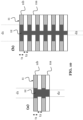
- The above described aspects and implementations are explained in the following description of embodiments with respect to the enclosed drawings:
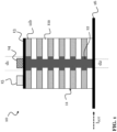
- FIG. 1
- shows an example of a magnetic memory device according to this disclosure with a top SOT track.
- FIG. 2
- shows another example of a magnetic memory device according to this disclosure with a bottom SOT track.
- FIG. 3
- shows another example of a magnetic memory device according to this disclosure with an out-of-plane MTJ.
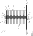
- FIG. 4
- shows another example of a magnetic memory device according to this disclosure with a bottom electrode.
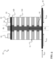
- FIG. 5
- shows another example of a magnetic memory device according to this disclosure without the bottom electrode but with a further top electrode.
- FIG. 6
- shows an example of writing a magnetic bit into a magnetic memory device according to this disclosure.
- FIG. 7
- shows an example of pushing magnetic bits in a magnetic memory device according to this disclosure.
- FIG. 8
- shows a method of operating a magnetic memory device according to this disclosure.
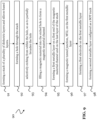
- FIG. 9
- shows a method of fabricating a magnetic memory device according to this disclosure.
- FIG. 10
- shows examples of recessed channels and layer stack heights, in order to control retention and latency for different performance specifications.
- Fig. 11
- another example of a magnetic memory device according to this disclosure with a SOT liner.
-
FIG. 1 shows an example of a 3Dmagnetic memory device 10 according to this disclosure. - Like all examples of
memory devices 10 presented in this disclosure, themagnetic memory device 10 ofFIG. 1 comprises alayer stack 11, which comprising a plurality ofdielectric layers 11a and silicon-basedlayers 11b, which are alternatingly arranged one on the other. Through thisstack 11 amagnetic material channel 12 is formed. Themagnetic material channel 12 extends through eachlayer stack 11. Themagnetic material channel 12 may extend along a first direction, which corresponds to a stacking direction of thelayers stack 11. This first direction may be referred to as `vertical direction', as oriented inFIG. 1 . Themagnetic material channel 12 may thus extend perpendicular to the surfaces of the layers of thestack 11. However, it is also possible that themagnetic material channel 12 extends in a slight angle to the surfaces of thelayers - As can be further seen in
FIG. 1 , and is common to all examples ofmagnetic memory devices 10 presented in this disclosure, themagnetic material channel 12 has a first diameter d1 where it extends through a silicon-basedlayer 11b, and has a second diameter d2 where it extends through adielectric layer 11a of thestack 11. That is, the at least onemagnetic material channel 12 has a varying diameter. This may be caused by partly recessing either the silicon-basedlayers 11b or thedielectric layers 11a of thestack 11 during the fabrication of thememory device 10, before forming themagnetic material channel 12. For example, the first diameter may be larger than the second diameter as shown inFIG. 1 , but this can also be the other way around. - Due to the alternation of the
layers stack 11, and further enhanced by the varying diameter of themagnetic material channel 12, a plurality of pinning sites, defined by the plurality oflayers magnetic material channel 12. Each of these pinning sites is configured to store one magnetic bit. It may be beneficial for the pinning sites, that the transitions between the first diameter d1 and the second diameter d2 are aligned with interfaces between the alternatingly arrangedlayers stack 11. - The
magnetic memory device 10 of each example in this disclosure, as is shown inFIG. 1 , further comprises a firstmetallic layer 13, which is arranged on a first end of themagnetic material channel 12 and on the last layer of thestack 11. The 'last layer' relates to the arrangement of the layers along the stacking direction of thelayers stack 11, from a first layer of the stack to the last layer of thestack 11. On the firstmetallic layer 13, aMTJ 14 is arranged. In addition, a first electrode 15 (also referred to as `top electrode') is arranged on the firstmetallic layer 13 at a distance to theMTJ 14. TheMTJ 14 comprises at least a free layer, a reference layer, and a tunnel barrier layer, so that it enables measuring TMR as known from conventional MRAM. Advantageously, theMTJ 14 may comprises a magnetic free layer having a coercivity of equal to or less than 20-40 mT, or in a range of 2-3 mT. - As shown for the example of
FIG. 1 , theMTJ 14 may be arranged directly above the first end of themagnetic material channel 12 on the firstmetallic layer 13. - As also shown for the example of
FIG. 1 , themagnetic memory device 10 may comprise a secondmetallic layer 16, which is configured as an SOT track. The second end of themagnetic material channel 12 and the first layer of thestack 11 are arranged on the secondmetallic layer 16 in this case. Being configured as an SOT track means that the secondmetallic layer 16 may be made of a certain material, have a certain thickness, and may be connected to suitable electrodes, in order to allow passing an SOT current (ISOT) through the secondmetallic layer 16, which causes a magnetic bit to be written by SOT into the pinning site defined by the layer of thestack 11 that is closest to the secondmetallic layer 16, as will be explained later. -
FIG. 2 shows another example of a 3Dmagnetic memory device 10 according to this disclosure. Same elements of thememory devices 10 inFIG. 1 andFIG. 2 share the same reference signs. - As shown for the example of
FIG. 2 , instead of comprising the secondmetallic layer 16 like the magnetic memory device ofFIG. 1 , the firstmetallic layer 13 may be configured as a SOT track. That is, the firstmetallic layer 13 may be made of a certain material, have a certain thickness, and may be connected to suitable electrodes, to allow passing an SOT current ISOT through thelayer 13, which causes a magnetic bit to be written by SOT into the pinning site defined by the layer of thestack 11 that is closest to the firstmetallic layer 13. - At least one of the first
metallic layer 13 and the secondmetallic layer 16, particularly at least themetallic layer -
FIG. 3 shows another example of a 3Dmagnetic memory device 10 according to this disclosure. Same elements of thememory devices 10 inFIG. 3 and in the previous figures share the same reference signs. - As show for the example of
FIG. 3 , theMTJ 14 may also be arranged offset from the first end of the magnetic material channel, i.e., is in this case not positioned directly above said first end of thechannel 12. TheMTJ 14 may thus be either closer to or further away from thefirst electrode 15 as in the first and second examples shown inFIGs. 1 and2 . TheMTJ 14 is also referred to as being arranged out-of-plane in this case. -
FIG. 4 shows another example of a 3Dmagnetic memory device 10 according to this disclosure. Same elements of thememory devices 10 shown inFIG. 4 and the previous figures share the same reference signs. The example ofFIG. 4 builds particularly on the example ofFIG. 1 , but the following features are also applicable to themagnetic memory devices 10 of the examples ofFIGs. 2 and3 . - As shown for the example of
FIG. 4 , themagnetic memory device 10 may comprise a second electrode 41 (Also referred to as `bottom electrode'), which is arranged on or directly below a second end of themagnetic material channel 12. Thesecond electrode 41 may be placed on the secondmetallic layer 16, as shown. However, in the absence of the secondmetallic layer 16, like in the example ofFIG. 2 , thesecond electrode 41 could be placed directly on the second end of themagnetic material channel 12 and the first layer of thestack 11. Thesecond electrode 41 may allow sending a push current IPush into themagnetic material channel 12 and towards thefirst electrode 15. -
FIG. 5 shows another example of a 3Dmagnetic memory device 10 according to this disclosure. Same elements of thememory devices 10 shown inFIG. 5 and the previous figures share the same reference signs. The example ofFIG. 4 builds particularly on the example ofFIG. 1 . - As shown for the example of
FIG. 5 , themagnetic memory device 10 may comprise a further first electrode 51 (also referred to as `further top electrode'). Further, themagnetic memory device 10 may comprise nosecond electrode 41 at the bottom, as inFIG. 4 . Without thesecond electrode 41, a more compact memory cell of thememory device 10 may be obtained, which may lead to a smaller footprint of thememory device 10 comprising multiple such memory cells. In the example ofFIG. 5 , the push current IPush may be provided by sending current through both sides of the SOT track provided by the secondmetallic layer 16. In particular, the current is pushed from both sides to limit the current density in the secondmetallic layer 16, and to increase its endurance and reliability. -
FIG. 6 shows an example of writing a magnetic bit into amagnetic memory device 10 according to this disclosure.FIG. 6 shows in particular the example ofFIG. 4 for demonstrating the writing operation.FIG. 6(a) shows themagnetic memory device 10 before/during the writing operation, whileFIG. 6(b) shows themagnetic memory device 10 after the writing operation. - The writing of the magnetic bit into the
magnetic material channel 12 is caused by passing the current ISOT through the secondmetallic layer 16, which is configured as the SOT track. The magnetic bit is written into the pinning site in themagnetic material channel 12, which is closest to the SOT track, i.e., the pinning site corresponding to the first layer of thechannel 12. A positive or negative current ISOT will determine the writing of the magnetic bit as 'up' or 'down' (for the case of perpendicular magnetization) or 'left' or 'right' (for the case of in-plane magnetization). For instance, inFIG. 6(b) , the writing of the magnetic bit has resulted in a switching of the bit, i.e., a switching of the magnetization in the corresponding pinning site. -
FIG. 7 shows an example of pushing magnetic bits in amagnetic memory device 10 according to this disclosure.FIG. 7 shows in particular the example ofFIG. 4 for demonstrating the pushing operation, following the writing operation shown inFIG. 6 . The pushing of the magnetic bits moves the magnetic bits along themagnetic material channel 12 from one pinning site to the next pinning site. As the example ofFIG. 4 is used, magnetic bits are pushed upwards in themagnetic material channel 12 inFIG. 7 , i.e., towards theMTJ 14. - The magnetic bits are pushed by passing a current IPush through the
first electrode 15. InFIG. 7 , the current is sent into thesecond electrode 41 towards thefirst electrode 15. If there would be nosecond electrode 41, the current IPush could be sent towards thefirst electrode 15 as illustrated inFIG. 5 , namely using the secondmetallic layer 16. During the pushing operation, a pulse timing may beneficially coincide with a domain wall movement of one period (one pinning site). The push current IPush will shift all magnetic bits (pinned magnetic domains) upwards by one pinning site. At the top of themagnetic channel 12 inFIG. 7 , the surface of the first end of themagnetic material channel 12 is advantageously flat, e.g., it may be flattened by chemical mechanic polishing (CMP). The firstmetallic layer 13 may function as a thin metallic spacer layer in this case (wherein it could be made of TaN), in order to provide a path for the current to go to thefirst electrode 15. - For reading a magnetic bit, the magnetic state of the uppermost magnetic bit may be sensed in the
magnetic memory device 10 according to the example ofFIG. 4 . This can be done by using the top-pinnedMTJ 14. The free layer of theMTJ 14 may be deposited in direct contact with the firstmetallic layer 13. The free layer may have the above-mentioned low coercivity of 40 mT or less, such that the stray magnetic field of the top magnetic bit (e.g., `up' or 'down', higher than the free layer coercivity) may determine the orientation of the free layer. The actual sensing can then be done by reading the resistance of theMTJ 14 and the TMR effect. - Since, in this example, the magnetic bit reaching the top of the magnetic channel 12 - which may be read using the MTJ 14 - will be annihilated at the next push, the read operation of the
magnetic memory device 10 may be a destructive read. The magnetic bit may then either be re-written at the bottom of themagnetic material channel 12, i.e., at the SOT track, or may be stored in a buffer memory, for instance, for a later burst write. - The
magnetic memory device 10 may, for example, operate in a `full string' writing and/or reading mode. This means that the smallest addressable bit-length may be equal to the number ofbilayers 11a/11b in thestack 11. However, the operation mode of themagnetic memory device 10 may also be determined by architectural choices on the array and system level. -
FIG. 8 shows amethod 80 of operating the 3Dmagnetic memory device 10, which summarizes generally the above-described. The method comprises at least one of the following operations: anoperation 81 of writing a magnetic bit into themagnetic material channel 12 by passing a current through the SOT track, wherein the magnetic bit is written into the pinning site in the magnetic material channel that is closest to the SOT track; anoperation 82 of pushing magnetic bits along themagnetic material channel 12 from one pinning site to the next pinning site by passing a current through thefirst electrode 15; anoperation 83 of reading a magnetic bit from themagnetic material channel 12 by passing a current through theMTJ 14 and thereby determining a TMR, wherein the magnetic bit stored in the pinning site in themagnetic material channel 12 that is closest to theMTJ 14 is read. - If the
magnetic memory device 10 comprises the second electrode 41 (like inFIG. 4 ), the pushing of the magnetic bits may comprise sending the current IPush from thesecond electrode 41 to thefirst electrode 15. If themagnetic memory device 10 does not comprise thesecond electrode 41, but comprises the secondmetallic layer 16 as the SOT track (like inFIG. 5 ), pushing the magnetic bits may comprise sending the current IPush from the secondmetallic layer 16 to thefirst electrode 15. If themagnetic memory device 10 comprises thesecond electrode 41 and the firstmetallic layer 13 is configured as the SOT track (like inFIG. 2 but with thesecond electrode 41 arranged beneath the second end of the magnetic material channel 12), pushing the magnetic bits may comprise sending a bi-polar current from the secondmetallic layer 16 to thefirst electrode 15. -
FIG. 9 shows amethod 90 of this disclosure of fabricating the 3Dmagnetic memory device 10. Themethod 90 comprise astep 91 of forming thestack 11 of a plurality ofdielectric layers 11a and silicon-basedlayers 11b, which are alternatingly arranged one on the other. Themethod 90 further comprises astep 92 of forming a hole through thestack 11, wherein the hole extends through thelayers stack 11. Themethod 90 then comprises astep 93 of selectively etching from within the hole, in order to recess either thedielectric layers 11a or the silicon-basedlayers 11b, so as to partially broaden the hole. Themethod 90 then comprises astep 94 of filling a magnetic material into the etched hole to form themagnetic material channel 12, which has the first diameter d1 where it extends through a silicon-basedlayer 11b of the stack and the second diameter d2 where it extends through adielectric layer 11a of thestack 11. - The
method 90 further comprises astep 95 of forming the firstmetallic layer 13 on the first end of themagnetic material channel 12 and on the last layer of thestack 11, and astep 96 of forming theMTJ 14 on the firstmetallic layer 13. Then, the method further comprises astep 97 of forming thefirst electrode 15 on the firstmetallic layer 13 at a distance to theMTJ 14. - If the
magnetic memory device 10 comprises the firstmetallic layer 13 as SOT track (like inFIG. 2 ), themethod 90 may be complete at this point. Alternatively, themethod 90 may further comprise astep 97 of forming a secondmetallic layer 16 configured as a SOT track (as inFIG. 1 ) and arranging the second end of themagnetic material channel 12 and the first layer of thestack 11 on the secondmetallic layer 16. -
FIG. 10 shows examples of differently recessedmagnetic material channels 12 and layer stack heights, which can be applied in any example of themagnetic memory device 10 of this disclosure. The various configurations may allow controlling a retention time and a latency of themagnetic memory device 10, which may be useful for complying with different performance specifications. In the example ofFIG. 10 , the first diameter d1 is larger than the second diameter d2. - Generally, a ratio between the first diameter d1 and the second diameter d2 may be in a range of 1.1:1 to 2:1. The transitions between the first diameter d1 and the second diameter d2 are advantageously aligned with interfaces between the alternatingly arranged
layers stack 11. Furthermore, a thickness t1 of the silicon-basedlayers 11b and a thickness t2 of thedielectric layers 11a may, respectively, in range of 5-150 nm.Same layers - Specifically,
FIG. 10(a) shows an example of the magnetic material channel recess, which reduces retention, but is beneficial for latency. The number oflayers stack 11 may be comparatively small, for example only in the order of 2-10 of each. Moreover, the recess may be comparatively small, for example, the ratio between the first diameter d1 and the second diameter d2 may be in a range of 1.1:1 to 4:3. -
FIG. 10(b) shows an example of the magnetic material channel recess, which reduces latency, but is beneficial for retention, i.e., increases retention. The number oflayers stack 11 may be comparatively large, particularly larger than inFIG. 10(b) , for example, in the order of 10-50 of each. Moreover, the recess may be comparatively small, particularly larger than inFIG. 10(b) , for example, the ratio between the first diameter d1 and the second diameter d2 may be in a range of 3:2 to 2:1. - For example, after creating the hole in the
stack 11, a selective etch can be applied to recess either layer material. This allows for controlling or adjusting the diameter of themagnetic material channel 12. This may strongly improve the domain wall movement, placement and dimension. The tuning of the recess (and hence, magnetic channel diameter variation) enables adjusting the domain pinning strength to achieve good operating window or adjust retention requirements. This also open the path for tailored performance. For example, one could imagine a limited height bit stack with low pinning to operate closer to DRAM latency and endurance, or a very tall stack with high pinning to cover 3D-NAND and archival specifications. -
FIG. 11 shows another example of amagnetic memory device 10 according to this disclosure. Same elements of thememory devices 10 inFIG. 11 and in the previous figures share the same reference signs. The example ofFIG. 11 particularly builds on the examples ofFIG. 4 and5 , wherein themagnetic memory device 10 ofFIG. 11 includes both the furtherfirst electrode 51 ofFIG. 5 and thesecond electrode 41 ofFIG. 4 - As shown for the example of
FIG. 11 , themagnetic memory device 10 may comprise a liner (e.g., a sheet) of SOT track material, i.e., a SOT material liner, on the interfaces of themagnetic material channel 12 and thelayers layer stack 11, before magnetic material is filled into the hole to form themagnetic material channel 12. The liner may increase the domain wall movement efficiency, and hence may reduce the push current IPush. Ideally the liner material is the same as, or at least similar to, the material of the SOT track, for reasons of compatibility (but this is not a must). - In all examples of this disclosure, the
dielectric layers 11a may be silicon oxide layers and the silicon-basedlayers 11b may be silicon nitride layers. Alternatively, teedielectric layers 11a may be silicon layers and the silicon-based layers may be silicon germanium layers. - In all examples of this disclosure, the magnetic material channel may be made of a ferromagnetic or ferrimagnetic material and/or a conductive material, for example, is made of cobalt, iron, nickel, or an alloys thereof, or any of the former in addition to boron.
- In summary, this disclosure propose a
magnetic memory device 10 that relies on a vertical arrangement of magnetic domains in a magnetic material channel 12 (e.g., a magnetic material wire) to store magnetic bits. Domain pinning (for high retention) can be achieved using thelayer stack 11, for instance, providing a Sin/SiO matrix, of which the morphology can be tuned to enhance or reduce pinning. Writing magnetic bits occurs via SOT at one end of the stack. Domain wall transport may be achieved by applying a current to themagnetic material channel 12 itself, and read-out may occurs where theMTJ 14 is used to sense the magnetic stray field of the closest domain. - In the claims as well as in the description of this disclosure, the word 'comprising' does not exclude other elements or steps and the indefinite article 'a' or 'an' does not exclude a plurality. A single element may fulfill the functions of several entities or items recited in the claims. The mere fact that certain measures are recited in the mutual different dependent claims does not indicate that a combination of these measures cannot be used in an advantageous implementation.
Claims (16)
- A three dimensional, 3D, magnetic memory device (10), the magnetic memory device (10) comprising:a stack (11) comprising a plurality of dielectric layers (11a) and silicon-based layers (11b), which are alternatingly arranged one on the other;a magnetic material channel (12) formed through the stack (11),wherein the magnetic material channel (12) extends through each layer (11a, 11b) of the stack (11),wherein the magnetic material channel (12) has a first diameter (d1) where it extends through a silicon-based layer (11b) and a second diameter (d2) where it extends through a dielectric layer (11a) of the stack (11), andwherein a plurality of pinning sites defined by the plurality of layers (11a, 11b) of the stack is formed in the magnetic material channel (12), each pinning site being configured to store one magnetic bit;a first metallic layer (13) arranged on a first end of the magnetic material channel (12) and on the last layer of the stack (11);a magnetic tunnel junction, MTJ, (14) arranged on the first metallic layer (13); anda first electrode (15) arranged on the first metallic layer (13) at a distance to the MTJ;wherein either the first metallic layer (13) is configured as a spin-orbit-torque, SOT, track, or the magnetic memory device (10) comprises a second metallic layer (16) configured as a SOT track and a second end of the magnetic material channel (12) and the first layer of the stack (11) are arranged on the second metallic layer (16).
- The 3D magnetic memory device (10) of claim 1, further comprising a second electrode (41) arranged on or directly below a second end of the magnetic material channel (12).
- The 3D magnetic memory device (10) of claim 1 or 2, wherein the first diameter (d1) is larger than the second diameter (d2).
- The 3D magnetic memory device (10) of one of the claims 1 to 3, wherein a ratio between the first diameter (d1) and the second diameter (d2) is in a range of 1.1:1 to 2:1.
- The 3D magnetic memory device (10) of one of the claims 1 to 4, wherein a thickness of the silicon-based layers (11b) and the dielectric layers (11a) is respectively in range of 5-150 nm.
- The 3D magnetic memory device (10) of one of the claims 1 to 5, wherein transitions between the first diameter (d1) and the second diameter (d2) are aligned with interfaces between the alternatingly arranged layers of the stack (11).
- The 3D magnetic memory device (10) of one of the claims 1 to 6, wherein:the dielectric layers (11a) are silicon oxide layers and the silicon-based layers (11b) are silicon nitride layers; orthe dielectric layers (11a) are silicon layers and the silicon-based layers (!1b) are silicon germanium layers.
- The 3D magnetic memory device (10) of one of the claims 1 to 7, wherein the magnetic material channel (12) is made of a ferromagnetic or ferrimagnetic material and/or a conductive material, for example, is made of cobalt, iron, nickel, or an alloys thereof, or any of the former in addition to boron.
- The 3D magnetic memory device (10) of one of the claims 1 to 8, wherein at least one of the first metallic layer (13) and the second metallic layer (16) is made of tantalum nitride, tungsten nitride, tungsten, tantalum, platinum, hafnium, molybdenum, molybdenum nitride, or alloys thereof, or is made of a topological insulator.
- The 3D magnetic memory device (10) of one of the claims 1 to 9, wherein the MTJ (14) is arranged directly above the first end of the magnetic material channel (12) on the first metallic layer (13), or is arranged offset from the first end of the magnetic material channel (12).
- The 3D magnetic memory device (10) of one of the claims 1 to 10, wherein the MTJ (14) comprises a magnetic free layer having a coercivity of equal to or less than 20-40 mT, or a coercivity in a range of 2-3 mT.
- A method (80) of operating the 3D magnetic memory device (10) of any one of the claims 1 to 10, wherein the method (80) comprises at least one of the following operations:writing (81) a magnetic bit into the magnetic material channel (12) by passing a current through the SOT track, wherein the magnetic bit is written into the pinning site in the magnetic material channel (12) that is closest to the SOT track;pushing (82) magnetic bits along the magnetic material channel (12) from one pinning site to the next pinning site by passing a current through the first electrode (15);reading (83) a magnetic bit from the magnetic material channel (12) by passing a current through the MTJ (14) and thereby determining a tunnelmagnetoresistance, wherein the magnetic bit stored in the pinning site in the magnetic material channel (12) that is closest to the MTJ (14) is read.
- The method (80) of claim 12, wherein:the magnetic memory device (10) comprises the second electrode (41), and pushing the magnetic bits comprises sending the current from the second electrode (41) to the first electrode (15); orthe magnetic memory device (10) does not comprise the second electrode (41) but comprises the second metallic layer (16), and pushing (82) the magnetic bits comprises sending the current from the second metallic layer (16) to the first electrode (15); orthe magnetic memory device (10) comprises the second electrode (41) and the first metallic layer (13) is configured as the SOT track, and pushing (82) the magnetic bits comprises sending a bi-polar current from the second metallic layer (16) to the first electrode (15).
- The method (80) of claim 12 or 13, wherein when pushing (82) the magnetic bits stored in the magnetic material channel (12), the magnetic bit stored in the pinning site in the magnetic material channel (12) that is closest to the first metallic layer (13) is destructed, and the method (80) further comprises:
re-writing the destructed magnetic bit into the magnetic material channel (12) or storing the information corresponding to the destructed magnetic bit in a memory. - A method (90) of fabricating a 3D magnetic memory device (10), the method (90) comprising:forming (91) a stack (11) of a plurality of dielectric layers (11a) and silicon-based layers (11b), which are alternatingly arranged one on the other;forming (92) a hole through the stack (11), wherein the hole extends through the layers (11a, 11b) of the stack (11);selectively etching (93) from within the hole, in order to recess either the dielectric layers (11a) or the silicon-based layers (11b) so as to partially broaden the hole;filling (94) a magnetic material into the etched hole to form a magnetic material channel (12), which has a first diameter (d1) where it extends through a silicon-based layer (11b) of the stack (11) and a second diameter (d2) where it extends through a dielectric layer (11a) of the stack (11),wherein a plurality of stacked pinning sites defined by the plurality of layers (11a, 11b) of the stack (11) is formed in the magnetic material channel (12), each pinning site being configured to store one magnetic bit;forming (95) a first metallic layer (13) on a first end of the magnetic material channel (12) and on the last layer of the stack (11);forming (96) a magnetic tunnel junction, MTJ, (14) on the first metallic layer (13); andforming (97) a first electrode (15) on the first metallic layer (13) at a distance to the MTJ (14);wherein either the first metallic layer (3) is configured as a spin-orbit-torque, SOT, track, or the method (90) further comprises forming (98) a second metallic layer (16) configured as a SOT track and arranging a second end of the magnetic material channel (12) and the first layer of the stack (11) on the second metallic layer (16).
- The method (90) of claim 15, further comprising depositing a liner (no) of SOT track material on the walls of the hole, before filling the magnetic material into the hole.
Priority Applications (4)
| Application Number | Priority Date | Filing Date | Title |
|---|---|---|---|
| EP23189234.0A EP4503033B1 (en) | 2023-08-02 | 2023-08-02 | High density 3d magnetic memory device, method of operating and method of fabricating the same |
| CN202480050777.0A CN121620801A (en) | 2023-08-02 | 2024-07-12 | High density 3D magnetic memory device |
| KR1020267006291A KR20260041146A (en) | 2023-08-02 | 2024-07-12 | High-density 3D magnetic memory device |
| PCT/EP2024/069790 WO2025026697A1 (en) | 2023-08-02 | 2024-07-12 | A high density 3d magnetic memory device |
Applications Claiming Priority (1)
| Application Number | Priority Date | Filing Date | Title |
|---|---|---|---|
| EP23189234.0A EP4503033B1 (en) | 2023-08-02 | 2023-08-02 | High density 3d magnetic memory device, method of operating and method of fabricating the same |
Publications (2)
| Publication Number | Publication Date |
|---|---|
| EP4503033A1 true EP4503033A1 (en) | 2025-02-05 |
| EP4503033B1 EP4503033B1 (en) | 2026-01-28 |
Family
ID=87554292
Family Applications (1)
| Application Number | Title | Priority Date | Filing Date |
|---|---|---|---|
| EP23189234.0A Active EP4503033B1 (en) | 2023-08-02 | 2023-08-02 | High density 3d magnetic memory device, method of operating and method of fabricating the same |
Country Status (4)
| Country | Link |
|---|---|
| EP (1) | EP4503033B1 (en) |
| KR (1) | KR20260041146A (en) |
| CN (1) | CN121620801A (en) |
| WO (1) | WO2025026697A1 (en) |
Citations (3)
| Publication number | Priority date | Publication date | Assignee | Title |
|---|---|---|---|---|
| US20200303624A1 (en) * | 2019-03-19 | 2020-09-24 | Toshiba Memory Corporation | Magnetic memory |
| US20210125653A1 (en) * | 2019-10-29 | 2021-04-29 | Samsung Electronics Co., Ltd. | Race track magnetic memory device and writing method thereof |
| US20210295889A1 (en) * | 2020-03-23 | 2021-09-23 | Kioxia Corporation | Magnetic memory |
-
2023
- 2023-08-02 EP EP23189234.0A patent/EP4503033B1/en active Active
-
2024
- 2024-07-12 WO PCT/EP2024/069790 patent/WO2025026697A1/en active Pending
- 2024-07-12 CN CN202480050777.0A patent/CN121620801A/en active Pending
- 2024-07-12 KR KR1020267006291A patent/KR20260041146A/en active Pending
Patent Citations (3)
| Publication number | Priority date | Publication date | Assignee | Title |
|---|---|---|---|---|
| US20200303624A1 (en) * | 2019-03-19 | 2020-09-24 | Toshiba Memory Corporation | Magnetic memory |
| US20210125653A1 (en) * | 2019-10-29 | 2021-04-29 | Samsung Electronics Co., Ltd. | Race track magnetic memory device and writing method thereof |
| US20210295889A1 (en) * | 2020-03-23 | 2021-09-23 | Kioxia Corporation | Magnetic memory |
Also Published As
| Publication number | Publication date |
|---|---|
| WO2025026697A1 (en) | 2025-02-06 |
| EP4503033B1 (en) | 2026-01-28 |
| KR20260041146A (en) | 2026-03-26 |
| CN121620801A (en) | 2026-03-06 |
Similar Documents
| Publication | Publication Date | Title |
|---|---|---|
| EP2515306B1 (en) | An improved high capacity low cost multi-state magnetic memory | |
| US10600460B2 (en) | Perpendicular magnetic memory using spin-orbit torque | |
| CN1819023B (en) | System and method for transferring data to a magnetic shift register with shiftable data columns | |
| US11882706B2 (en) | One selector one resistor MRAM crosspoint memory array fabrication methods | |
| JP4538067B2 (en) | Semiconductor memory device | |
| JP4846817B2 (en) | Resistance change memory | |
| US7710757B2 (en) | Magnetic track using magnetic domain wall movement and information storage device including the same | |
| US20090046501A1 (en) | Low-cost non-volatile flash-ram memory | |
| JP5677347B2 (en) | Magnetoresistive element and magnetic memory writing method | |
| CN1427416A (en) | Magnetic storage device with soft reference layer | |
| US10783943B2 (en) | MRAM having novel self-referenced read method | |
| JP2003197876A (en) | Magnetic RAM | |
| US9190167B2 (en) | Shift register and shift register type magnetic memory | |
| TWI799097B (en) | Forced current access with voltage clamping in cross-point array | |
| KR102427526B1 (en) | Random access memory | |
| CN106783862A (en) | A kind of STT mram memory cells | |
| US9236561B2 (en) | Method and system for providing multiple self-aligned logic cells in a single stack | |
| EP4503033B1 (en) | High density 3d magnetic memory device, method of operating and method of fabricating the same | |
| CN102683581B (en) | Voltage-adjustable reluctance-variable random memory cell and random memory | |
| EP4560635A1 (en) | A high density 3d magnetic memory device | |
| CN113257296B (en) | Memory array | |
| US12361996B1 (en) | System and method for spin orbit torque based memory device | |
| CN1902685A (en) | Solid state magnetic memory system and method | |
| KR20080061765A (en) | MRAM-PRMA composite memory device and method of manufacturing the same | |
| KR101497541B1 (en) | Magnetic memory element and information recording method |
Legal Events
| Date | Code | Title | Description |
|---|---|---|---|
| PUAI | Public reference made under article 153(3) epc to a published international application that has entered the european phase |
Free format text: ORIGINAL CODE: 0009012 |
|
| STAA | Information on the status of an ep patent application or granted ep patent |
Free format text: STATUS: THE APPLICATION HAS BEEN PUBLISHED |
|
| AK | Designated contracting states |
Kind code of ref document: A1 Designated state(s): AL AT BE BG CH CY CZ DE DK EE ES FI FR GB GR HR HU IE IS IT LI LT LU LV MC ME MK MT NL NO PL PT RO RS SE SI SK SM TR |
|
| STAA | Information on the status of an ep patent application or granted ep patent |
Free format text: STATUS: REQUEST FOR EXAMINATION WAS MADE |
|
| 17P | Request for examination filed |
Effective date: 20250602 |
|
| REG | Reference to a national code |
Ref country code: DE Ref legal event code: R079 Free format text: PREVIOUS MAIN CLASS: G11C0011160000 Ipc: H10B0061000000 Ref country code: DE Ref legal event code: R079 Ref document number: 602023011207 Country of ref document: DE Free format text: PREVIOUS MAIN CLASS: G11C0011160000 Ipc: H10B0061000000 |
|
| RIC1 | Information provided on ipc code assigned before grant |
Ipc: H10B 61/00 20230101AFI20250923BHEP Ipc: G11C 11/16 20060101ALI20250923BHEP Ipc: G11C 11/18 20060101ALI20250923BHEP Ipc: G11C 19/08 20060101ALI20250923BHEP |
|
| GRAP | Despatch of communication of intention to grant a patent |
Free format text: ORIGINAL CODE: EPIDOSNIGR1 |
|
| STAA | Information on the status of an ep patent application or granted ep patent |
Free format text: STATUS: GRANT OF PATENT IS INTENDED |
|
| INTG | Intention to grant announced |
Effective date: 20251111 |
|
| GRAS | Grant fee paid |
Free format text: ORIGINAL CODE: EPIDOSNIGR3 |
|
| GRAA | (expected) grant |
Free format text: ORIGINAL CODE: 0009210 |
|
| STAA | Information on the status of an ep patent application or granted ep patent |
Free format text: STATUS: THE PATENT HAS BEEN GRANTED |
|
| AK | Designated contracting states |
Kind code of ref document: B1 Designated state(s): AL AT BE BG CH CY CZ DE DK EE ES FI FR GB GR HR HU IE IS IT LI LT LU LV MC ME MK MT NL NO PL PT RO RS SE SI SK SM TR |
|
| REG | Reference to a national code |
Ref country code: CH Ref legal event code: F10 Free format text: ST27 STATUS EVENT CODE: U-0-0-F10-F00 (AS PROVIDED BY THE NATIONAL OFFICE) Effective date: 20260128 Ref country code: GB Ref legal event code: FG4D |
|
| REG | Reference to a national code |
Ref country code: DE Ref legal event code: R096 Ref document number: 602023011207 Country of ref document: DE |
|
| REG | Reference to a national code |
Ref country code: IE Ref legal event code: FG4D |