EP4503004A1 - Display device - Google Patents
Display device Download PDFInfo
- Publication number
- EP4503004A1 EP4503004A1 EP23796747.6A EP23796747A EP4503004A1 EP 4503004 A1 EP4503004 A1 EP 4503004A1 EP 23796747 A EP23796747 A EP 23796747A EP 4503004 A1 EP4503004 A1 EP 4503004A1
- Authority
- EP
- European Patent Office
- Prior art keywords
- sensing
- transistor
- scan
- electrode
- lines
- Prior art date
- Legal status (The legal status is an assumption and is not a legal conclusion. Google has not performed a legal analysis and makes no representation as to the accuracy of the status listed.)
- Pending
Links
Images



















Classifications
-
- G—PHYSICS
- G09—EDUCATION; CRYPTOGRAPHY; DISPLAY; ADVERTISING; SEALS
- G09G—ARRANGEMENTS OR CIRCUITS FOR CONTROL OF INDICATING DEVICES USING STATIC MEANS TO PRESENT VARIABLE INFORMATION
- G09G3/00—Control arrangements or circuits, of interest only in connection with visual indicators other than cathode-ray tubes
- G09G3/20—Control arrangements or circuits, of interest only in connection with visual indicators other than cathode-ray tubes for presentation of an assembly of a number of characters, e.g. a page, by composing the assembly by combination of individual elements arranged in a matrix no fixed position being assigned to or needed to be assigned to the individual characters or partial characters
- G09G3/22—Control arrangements or circuits, of interest only in connection with visual indicators other than cathode-ray tubes for presentation of an assembly of a number of characters, e.g. a page, by composing the assembly by combination of individual elements arranged in a matrix no fixed position being assigned to or needed to be assigned to the individual characters or partial characters using controlled light sources
- G09G3/30—Control arrangements or circuits, of interest only in connection with visual indicators other than cathode-ray tubes for presentation of an assembly of a number of characters, e.g. a page, by composing the assembly by combination of individual elements arranged in a matrix no fixed position being assigned to or needed to be assigned to the individual characters or partial characters using controlled light sources using electroluminescent panels
- G09G3/32—Control arrangements or circuits, of interest only in connection with visual indicators other than cathode-ray tubes for presentation of an assembly of a number of characters, e.g. a page, by composing the assembly by combination of individual elements arranged in a matrix no fixed position being assigned to or needed to be assigned to the individual characters or partial characters using controlled light sources using electroluminescent panels semiconductive, e.g. using light-emitting diodes [LED]
- G09G3/3208—Control arrangements or circuits, of interest only in connection with visual indicators other than cathode-ray tubes for presentation of an assembly of a number of characters, e.g. a page, by composing the assembly by combination of individual elements arranged in a matrix no fixed position being assigned to or needed to be assigned to the individual characters or partial characters using controlled light sources using electroluminescent panels semiconductive, e.g. using light-emitting diodes [LED] organic, e.g. using organic light-emitting diodes [OLED]
-
- G—PHYSICS
- G06—COMPUTING OR CALCULATING; COUNTING
- G06F—ELECTRIC DIGITAL DATA PROCESSING
- G06F3/00—Input arrangements for transferring data to be processed into a form capable of being handled by the computer; Output arrangements for transferring data from processing unit to output unit, e.g. interface arrangements
- G06F3/01—Input arrangements or combined input and output arrangements for interaction between user and computer
- G06F3/03—Arrangements for converting the position or the displacement of a member into a coded form
- G06F3/041—Digitisers, e.g. for touch screens or touch pads, characterised by the transducing means
- G06F3/0416—Control or interface arrangements specially adapted for digitisers
- G06F3/04164—Connections between sensors and controllers, e.g. routing lines between electrodes and connection pads
-
- G—PHYSICS
- G06—COMPUTING OR CALCULATING; COUNTING
- G06F—ELECTRIC DIGITAL DATA PROCESSING
- G06F3/00—Input arrangements for transferring data to be processed into a form capable of being handled by the computer; Output arrangements for transferring data from processing unit to output unit, e.g. interface arrangements
- G06F3/01—Input arrangements or combined input and output arrangements for interaction between user and computer
- G06F3/03—Arrangements for converting the position or the displacement of a member into a coded form
- G06F3/041—Digitisers, e.g. for touch screens or touch pads, characterised by the transducing means
- G06F3/0416—Control or interface arrangements specially adapted for digitisers
- G06F3/04166—Details of scanning methods, e.g. sampling time, grouping of sub areas or time sharing with display driving
-
- G—PHYSICS
- G06—COMPUTING OR CALCULATING; COUNTING
- G06K—GRAPHICAL DATA READING; PRESENTATION OF DATA; RECORD CARRIERS; HANDLING RECORD CARRIERS
- G06K19/00—Record carriers for use with machines and with at least a part designed to carry digital markings
- G06K19/06—Record carriers for use with machines and with at least a part designed to carry digital markings characterised by the kind of the digital marking, e.g. shape, nature, code
- G06K19/067—Record carriers with conductive marks, printed circuits or semiconductor circuit elements, e.g. credit or identity cards also with resonating or responding marks without active components
- G06K19/07—Record carriers with conductive marks, printed circuits or semiconductor circuit elements, e.g. credit or identity cards also with resonating or responding marks without active components with integrated circuit chips
- G06K19/0716—Record carriers with conductive marks, printed circuits or semiconductor circuit elements, e.g. credit or identity cards also with resonating or responding marks without active components with integrated circuit chips at least one of the integrated circuit chips comprising a sensor or an interface to a sensor
- G06K19/0718—Record carriers with conductive marks, printed circuits or semiconductor circuit elements, e.g. credit or identity cards also with resonating or responding marks without active components with integrated circuit chips at least one of the integrated circuit chips comprising a sensor or an interface to a sensor the sensor being of the biometric kind, e.g. fingerprint sensors
-
- G—PHYSICS
- G06—COMPUTING OR CALCULATING; COUNTING
- G06V—IMAGE OR VIDEO RECOGNITION OR UNDERSTANDING
- G06V40/00—Recognition of biometric, human-related or animal-related patterns in image or video data
- G06V40/10—Human or animal bodies, e.g. vehicle occupants or pedestrians; Body parts, e.g. hands
- G06V40/12—Fingerprints or palmprints
- G06V40/13—Sensors therefor
- G06V40/1318—Sensors therefor using electro-optical elements or layers, e.g. electroluminescent sensing
-
- G—PHYSICS
- G09—EDUCATION; CRYPTOGRAPHY; DISPLAY; ADVERTISING; SEALS
- G09G—ARRANGEMENTS OR CIRCUITS FOR CONTROL OF INDICATING DEVICES USING STATIC MEANS TO PRESENT VARIABLE INFORMATION
- G09G3/00—Control arrangements or circuits, of interest only in connection with visual indicators other than cathode-ray tubes
- G09G3/20—Control arrangements or circuits, of interest only in connection with visual indicators other than cathode-ray tubes for presentation of an assembly of a number of characters, e.g. a page, by composing the assembly by combination of individual elements arranged in a matrix no fixed position being assigned to or needed to be assigned to the individual characters or partial characters
- G09G3/22—Control arrangements or circuits, of interest only in connection with visual indicators other than cathode-ray tubes for presentation of an assembly of a number of characters, e.g. a page, by composing the assembly by combination of individual elements arranged in a matrix no fixed position being assigned to or needed to be assigned to the individual characters or partial characters using controlled light sources
- G09G3/30—Control arrangements or circuits, of interest only in connection with visual indicators other than cathode-ray tubes for presentation of an assembly of a number of characters, e.g. a page, by composing the assembly by combination of individual elements arranged in a matrix no fixed position being assigned to or needed to be assigned to the individual characters or partial characters using controlled light sources using electroluminescent panels
- G09G3/32—Control arrangements or circuits, of interest only in connection with visual indicators other than cathode-ray tubes for presentation of an assembly of a number of characters, e.g. a page, by composing the assembly by combination of individual elements arranged in a matrix no fixed position being assigned to or needed to be assigned to the individual characters or partial characters using controlled light sources using electroluminescent panels semiconductive, e.g. using light-emitting diodes [LED]
- G09G3/3208—Control arrangements or circuits, of interest only in connection with visual indicators other than cathode-ray tubes for presentation of an assembly of a number of characters, e.g. a page, by composing the assembly by combination of individual elements arranged in a matrix no fixed position being assigned to or needed to be assigned to the individual characters or partial characters using controlled light sources using electroluminescent panels semiconductive, e.g. using light-emitting diodes [LED] organic, e.g. using organic light-emitting diodes [OLED]
- G09G3/3225—Control arrangements or circuits, of interest only in connection with visual indicators other than cathode-ray tubes for presentation of an assembly of a number of characters, e.g. a page, by composing the assembly by combination of individual elements arranged in a matrix no fixed position being assigned to or needed to be assigned to the individual characters or partial characters using controlled light sources using electroluminescent panels semiconductive, e.g. using light-emitting diodes [LED] organic, e.g. using organic light-emitting diodes [OLED] using an active matrix
- G09G3/3233—Control arrangements or circuits, of interest only in connection with visual indicators other than cathode-ray tubes for presentation of an assembly of a number of characters, e.g. a page, by composing the assembly by combination of individual elements arranged in a matrix no fixed position being assigned to or needed to be assigned to the individual characters or partial characters using controlled light sources using electroluminescent panels semiconductive, e.g. using light-emitting diodes [LED] organic, e.g. using organic light-emitting diodes [OLED] using an active matrix with pixel circuitry controlling the current through the light-emitting element
-
- H—ELECTRICITY
- H10—SEMICONDUCTOR DEVICES; ELECTRIC SOLID-STATE DEVICES NOT OTHERWISE PROVIDED FOR
- H10K—ORGANIC ELECTRIC SOLID-STATE DEVICES
- H10K39/00—Integrated devices, or assemblies of multiple devices, comprising at least one organic radiation-sensitive element covered by group H10K30/00
- H10K39/30—Devices controlled by radiation
- H10K39/32—Organic image sensors
- H10K39/34—Organic image sensors integrated with organic light-emitting diodes [OLED]
-
- H—ELECTRICITY
- H10—SEMICONDUCTOR DEVICES; ELECTRIC SOLID-STATE DEVICES NOT OTHERWISE PROVIDED FOR
- H10K—ORGANIC ELECTRIC SOLID-STATE DEVICES
- H10K59/00—Integrated devices, or assemblies of multiple devices, comprising at least one organic light-emitting element covered by group H10K50/00
- H10K59/10—OLED displays
- H10K59/12—Active-matrix OLED [AMOLED] displays
- H10K59/131—Interconnections, e.g. wiring lines or terminals
-
- H—ELECTRICITY
- H10—SEMICONDUCTOR DEVICES; ELECTRIC SOLID-STATE DEVICES NOT OTHERWISE PROVIDED FOR
- H10K—ORGANIC ELECTRIC SOLID-STATE DEVICES
- H10K59/00—Integrated devices, or assemblies of multiple devices, comprising at least one organic light-emitting element covered by group H10K50/00
- H10K59/40—OLEDs integrated with touch screens
-
- H—ELECTRICITY
- H10—SEMICONDUCTOR DEVICES; ELECTRIC SOLID-STATE DEVICES NOT OTHERWISE PROVIDED FOR
- H10K—ORGANIC ELECTRIC SOLID-STATE DEVICES
- H10K59/00—Integrated devices, or assemblies of multiple devices, comprising at least one organic light-emitting element covered by group H10K50/00
- H10K59/60—OLEDs integrated with inorganic light-sensitive elements, e.g. with inorganic solar cells or inorganic photodiodes
-
- G—PHYSICS
- G09—EDUCATION; CRYPTOGRAPHY; DISPLAY; ADVERTISING; SEALS
- G09G—ARRANGEMENTS OR CIRCUITS FOR CONTROL OF INDICATING DEVICES USING STATIC MEANS TO PRESENT VARIABLE INFORMATION
- G09G2300/00—Aspects of the constitution of display devices
- G09G2300/04—Structural and physical details of display devices
- G09G2300/0421—Structural details of the set of electrodes
- G09G2300/0426—Layout of electrodes and connections
-
- G—PHYSICS
- G09—EDUCATION; CRYPTOGRAPHY; DISPLAY; ADVERTISING; SEALS
- G09G—ARRANGEMENTS OR CIRCUITS FOR CONTROL OF INDICATING DEVICES USING STATIC MEANS TO PRESENT VARIABLE INFORMATION
- G09G2300/00—Aspects of the constitution of display devices
- G09G2300/08—Active matrix structure, i.e. with use of active elements, inclusive of non-linear two terminal elements, in the pixels together with light emitting or modulating elements
- G09G2300/0809—Several active elements per pixel in active matrix panels
-
- G—PHYSICS
- G09—EDUCATION; CRYPTOGRAPHY; DISPLAY; ADVERTISING; SEALS
- G09G—ARRANGEMENTS OR CIRCUITS FOR CONTROL OF INDICATING DEVICES USING STATIC MEANS TO PRESENT VARIABLE INFORMATION
- G09G2300/00—Aspects of the constitution of display devices
- G09G2300/08—Active matrix structure, i.e. with use of active elements, inclusive of non-linear two terminal elements, in the pixels together with light emitting or modulating elements
- G09G2300/0809—Several active elements per pixel in active matrix panels
- G09G2300/0819—Several active elements per pixel in active matrix panels used for counteracting undesired variations, e.g. feedback or autozeroing
-
- G—PHYSICS
- G09—EDUCATION; CRYPTOGRAPHY; DISPLAY; ADVERTISING; SEALS
- G09G—ARRANGEMENTS OR CIRCUITS FOR CONTROL OF INDICATING DEVICES USING STATIC MEANS TO PRESENT VARIABLE INFORMATION
- G09G2300/00—Aspects of the constitution of display devices
- G09G2300/08—Active matrix structure, i.e. with use of active elements, inclusive of non-linear two terminal elements, in the pixels together with light emitting or modulating elements
- G09G2300/0809—Several active elements per pixel in active matrix panels
- G09G2300/0842—Several active elements per pixel in active matrix panels forming a memory circuit, e.g. a dynamic memory with one capacitor
-
- G—PHYSICS
- G09—EDUCATION; CRYPTOGRAPHY; DISPLAY; ADVERTISING; SEALS
- G09G—ARRANGEMENTS OR CIRCUITS FOR CONTROL OF INDICATING DEVICES USING STATIC MEANS TO PRESENT VARIABLE INFORMATION
- G09G2300/00—Aspects of the constitution of display devices
- G09G2300/08—Active matrix structure, i.e. with use of active elements, inclusive of non-linear two terminal elements, in the pixels together with light emitting or modulating elements
- G09G2300/0809—Several active elements per pixel in active matrix panels
- G09G2300/0842—Several active elements per pixel in active matrix panels forming a memory circuit, e.g. a dynamic memory with one capacitor
- G09G2300/0861—Several active elements per pixel in active matrix panels forming a memory circuit, e.g. a dynamic memory with one capacitor with additional control of the display period without amending the charge stored in a pixel memory, e.g. by means of additional select electrodes
-
- G—PHYSICS
- G09—EDUCATION; CRYPTOGRAPHY; DISPLAY; ADVERTISING; SEALS
- G09G—ARRANGEMENTS OR CIRCUITS FOR CONTROL OF INDICATING DEVICES USING STATIC MEANS TO PRESENT VARIABLE INFORMATION
- G09G2310/00—Command of the display device
- G09G2310/02—Addressing, scanning or driving the display screen or processing steps related thereto
- G09G2310/0202—Addressing of scan or signal lines
-
- G—PHYSICS
- G09—EDUCATION; CRYPTOGRAPHY; DISPLAY; ADVERTISING; SEALS
- G09G—ARRANGEMENTS OR CIRCUITS FOR CONTROL OF INDICATING DEVICES USING STATIC MEANS TO PRESENT VARIABLE INFORMATION
- G09G2310/00—Command of the display device
- G09G2310/02—Addressing, scanning or driving the display screen or processing steps related thereto
- G09G2310/0243—Details of the generation of driving signals
- G09G2310/0251—Precharge or discharge of pixel before applying new pixel voltage
-
- G—PHYSICS
- G09—EDUCATION; CRYPTOGRAPHY; DISPLAY; ADVERTISING; SEALS
- G09G—ARRANGEMENTS OR CIRCUITS FOR CONTROL OF INDICATING DEVICES USING STATIC MEANS TO PRESENT VARIABLE INFORMATION
- G09G2310/00—Command of the display device
- G09G2310/08—Details of timing specific for flat panels, other than clock recovery
-
- G—PHYSICS
- G09—EDUCATION; CRYPTOGRAPHY; DISPLAY; ADVERTISING; SEALS
- G09G—ARRANGEMENTS OR CIRCUITS FOR CONTROL OF INDICATING DEVICES USING STATIC MEANS TO PRESENT VARIABLE INFORMATION
- G09G2320/00—Control of display operating conditions
- G09G2320/02—Improving the quality of display appearance
- G09G2320/0209—Crosstalk reduction, i.e. to reduce direct or indirect influences of signals directed to a certain pixel of the displayed image on other pixels of said image, inclusive of influences affecting pixels in different frames or fields or sub-images which constitute a same image, e.g. left and right images of a stereoscopic display
- G09G2320/0214—Crosstalk reduction, i.e. to reduce direct or indirect influences of signals directed to a certain pixel of the displayed image on other pixels of said image, inclusive of influences affecting pixels in different frames or fields or sub-images which constitute a same image, e.g. left and right images of a stereoscopic display with crosstalk due to leakage current of pixel switch in active matrix panels
-
- G—PHYSICS
- G09—EDUCATION; CRYPTOGRAPHY; DISPLAY; ADVERTISING; SEALS
- G09G—ARRANGEMENTS OR CIRCUITS FOR CONTROL OF INDICATING DEVICES USING STATIC MEANS TO PRESENT VARIABLE INFORMATION
- G09G2320/00—Control of display operating conditions
- G09G2320/02—Improving the quality of display appearance
- G09G2320/029—Improving the quality of display appearance by monitoring one or more pixels in the display panel, e.g. by monitoring a fixed reference pixel
- G09G2320/0295—Improving the quality of display appearance by monitoring one or more pixels in the display panel, e.g. by monitoring a fixed reference pixel by monitoring each display pixel
-
- G—PHYSICS
- G09—EDUCATION; CRYPTOGRAPHY; DISPLAY; ADVERTISING; SEALS
- G09G—ARRANGEMENTS OR CIRCUITS FOR CONTROL OF INDICATING DEVICES USING STATIC MEANS TO PRESENT VARIABLE INFORMATION
- G09G2320/00—Control of display operating conditions
- G09G2320/04—Maintaining the quality of display appearance
- G09G2320/043—Preventing or counteracting the effects of ageing
- G09G2320/045—Compensation of drifts in the characteristics of light emitting or modulating elements
-
- G—PHYSICS
- G09—EDUCATION; CRYPTOGRAPHY; DISPLAY; ADVERTISING; SEALS
- G09G—ARRANGEMENTS OR CIRCUITS FOR CONTROL OF INDICATING DEVICES USING STATIC MEANS TO PRESENT VARIABLE INFORMATION
- G09G2354/00—Aspects of interface with display user
-
- G—PHYSICS
- G09—EDUCATION; CRYPTOGRAPHY; DISPLAY; ADVERTISING; SEALS
- G09G—ARRANGEMENTS OR CIRCUITS FOR CONTROL OF INDICATING DEVICES USING STATIC MEANS TO PRESENT VARIABLE INFORMATION
- G09G2360/00—Aspects of the architecture of display systems
- G09G2360/14—Detecting light within display terminals, e.g. using a single or a plurality of photosensors
-
- G—PHYSICS
- G09—EDUCATION; CRYPTOGRAPHY; DISPLAY; ADVERTISING; SEALS
- G09G—ARRANGEMENTS OR CIRCUITS FOR CONTROL OF INDICATING DEVICES USING STATIC MEANS TO PRESENT VARIABLE INFORMATION
- G09G2360/00—Aspects of the architecture of display systems
- G09G2360/14—Detecting light within display terminals, e.g. using a single or a plurality of photosensors
- G09G2360/141—Detecting light within display terminals, e.g. using a single or a plurality of photosensors the light conveying information used for selecting or modulating the light emitting or modulating element
- G09G2360/142—Detecting light within display terminals, e.g. using a single or a plurality of photosensors the light conveying information used for selecting or modulating the light emitting or modulating element the light being detected by light detection means within each pixel
-
- G—PHYSICS
- G09—EDUCATION; CRYPTOGRAPHY; DISPLAY; ADVERTISING; SEALS
- G09G—ARRANGEMENTS OR CIRCUITS FOR CONTROL OF INDICATING DEVICES USING STATIC MEANS TO PRESENT VARIABLE INFORMATION
- G09G2360/00—Aspects of the architecture of display systems
- G09G2360/14—Detecting light within display terminals, e.g. using a single or a plurality of photosensors
- G09G2360/145—Detecting light within display terminals, e.g. using a single or a plurality of photosensors the light originating from the display screen
- G09G2360/147—Detecting light within display terminals, e.g. using a single or a plurality of photosensors the light originating from the display screen the originated light output being determined for each pixel
- G09G2360/148—Detecting light within display terminals, e.g. using a single or a plurality of photosensors the light originating from the display screen the originated light output being determined for each pixel the light being detected by light detection means within each pixel
Definitions
- the present disclosure relates to a display device.
- a display device is applied to various electronic devices such as a smart phone, a tablet, a notebook computer, a monitor, and a TV.
- portable electronic devices such as smartphones, tablets, and notebook computers has greatly increased. Since privacy information is stored in a portable electronic device, fingerprint authentication for authenticating a user's biometric fingerprint is used to protect personal information of the portable electronic device.
- the display device may authenticate the user's fingerprint using an optical method, an ultrasonic method, a capacitive method, or the like.
- the optical method may authenticate the user's fingerprint by detecting light reflected from the user's fingerprint.
- the display device may include a display panel including display pixels for displaying an image and light sensing pixels for sensing light in order to optically authenticate a user's fingerprint.
- aspects and features of embodiments of the present disclosure provide a display device capable of reducing a decrease in fingerprint sensing capability due to an off-leakage current of a reset transistor of a light sensing pixel.
- display device includes display pixels each including a light emitting unit including a light emitting element and a pixel driving unit applying a driving current to the light emitting element, and light sensing pixels each including a light sensing unit including an optical element and a sensing driving unit for applying a sensing current to any one of the sensing lines according to the photocurrent of the optical element.
- the sensing driving unit includes a first sensing transistor for controlling a sensing current flowing through a sensing line according to a voltage of a first electrode of the optical element, and a second sensing transistor initializing the first electrode of the optical element to a first level voltage.
- a channel layer of the first sensing transistor and the channel layer of the second sensing transistor are made of different materials.
- display device includes scan write lines, scan initialization lines, scan control lines, and light emitting lines extending in a first direction, data lines and sensing lines extending in a second direction intersecting the first direction, display pixels each including a light emitting unit including a light emitting element and a pixel driving unit applying a driving current to the light emitting element according to a data voltage of one of the data lines, and light sensing pixels each including a light sensing unit including a optical element and a sensing driving unit for applying a sensing current to any one of the sensing lines according to a photocurrent of the optical element.
- the sensing driving unit of any one of the light sensing pixels is disposed on one side of the pixel driving unit of a first display pixel among the display pixels.
- the sensing driving unit of the first light sensing pixel overlaps at least one of the scan write lines, one of the scan initialization lines, one of the scan control lines, one of the light emitting lines, and at least one of the sensing lines.
- the display device since light sensing pixels for fingerprint detection are disposed in the entire display area, the display device may perform fingerprint authentication even if the user places a finger's fingerprint anywhere in the display area of the display panel.
- the area of the sensing driving unit may be minimized despite an increase in the number of pixels per unit area of the display panel, and thus the reduction in area of each of the first to fourth pixel driving units may be minimized.
- the second transistor and the third transistor of the pixel driving unit are formed of an N-type MOSFET
- at least one of the second sensing transistor and the third sensing transistor may be formed of an N-type MOSFET without a separate process. Therefore, by forming at least one of the second sensing transistor and the third sensing transistor as an N-type MOSFET, it is possible to reduce the decrease of the fingerprint sensing capability due to the off-leakage current of the second sensing transistor and/or the off-leakage current of the third sensing transistor.
- the pixel driving unit and a sensing driving unit share at least one of a scan control line, a scan initialization line, a light emitting line, and a scan bias line, a first power supply line, and a second power supply line. Therefore, there is an advantage in that there is no need for a separate wire to which a separate signal for driving the sensing driving unit is applied even though the sensing driving unit is added.
- each feature of the various embodiments of the present invention can be partially or entirely combined or combined with each other, technically various interlocking and driving are possible, and each embodiment can be implemented independently of each other or can be implemented together in a related relationship.
- FIG. 1 is a perspective view illustrating a display device according to one or more embodiments.
- a display device 10 is a device for displaying a moving image or a still image.
- the display device may be used as a display screen of various products such as televisions, laptop computers, monitors, billboards and the Internet of Things (IOT) as well as portable electronic devices such as mobile phones, smart phones, tablet personal computer (tablet PC), smart watches, watch phones, mobile communication terminals, electronic notebooks, electronic books, portable multimedia players (PMPs), navigation systems and ultra mobile PCs (UMPCs).
- IOT Internet of Things
- portable electronic devices such as mobile phones, smart phones, tablet personal computer (tablet PC), smart watches, watch phones, mobile communication terminals, electronic notebooks, electronic books, portable multimedia players (PMPs), navigation systems and ultra mobile PCs (UMPCs).
- PMPs portable multimedia players
- UMPCs ultra mobile PCs
- the display device 10 may be a light emitting display device such as an organic light emitting display device using an organic light emitting diode, a quantum dot light emitting display including a quantum dot light emitting layer, an inorganic light emitting display including an inorganic semiconductor, and a micro or nano light emitting display device using a micro or nano light emitting diode (micro LED or nano LED).
- a light emitting display device such as an organic light emitting display device using an organic light emitting diode, a quantum dot light emitting display including a quantum dot light emitting layer, an inorganic light emitting display including an inorganic semiconductor, and a micro or nano light emitting display device using a micro or nano light emitting diode (micro LED or nano LED).
- the display device 10 has been mainly described as an organic light emitting display device, but the present disclosure is not limited thereto.
- the display device 10 includes a display panel 100, a display driving circuit 200, and a circuit board 400.
- the display panel 100 may be formed in a rectangular plane having a short side in a first direction DR1 and a long side in a second direction DR2 intersecting the first direction DR1.
- a corner where a short side of the first direction DR1 and a long side of the second direction DR2 meet may be formed at a right angle may or may be rounded to have a predetermined curvature.
- a flat shape of the display panel 100 is not limited to a quadrangle, and may be formed in other polygons, circles, or ovals.
- the display panel 100 may be formed to be flat but is not limited thereto.
- the display panel 100 is formed at left and right ends and may include curved portions having a constant curvature or a varying curvature.
- the display panel 100 may be flexibly formed to be curved, crooked, bent, folded, or rolled.
- a substrate SUB of the display panel 100 may include a main area MA and a sub area SBA.
- the main area MA may include a display area DA displaying an image and a non-display area NDA that is a peripheral area of the display area DA.
- the display area DA may include display pixels (PXs of FIG. 2 ) that display an image.
- the display area DA may include light sensing pixels (PS of FIG. 2 ) that sense light to not only display an image but also detect a user's fingerprint.
- the display area DA may occupy most of the main area MA.
- the display area DA may be disposed in the center of the main area MA.
- FIG. 1 it was exemplified that a sub-region SBA is unfolded, but the sub-region SBA may be bent. Also, the sub-region SBA may be overlapped with the main area MA since the sub-region SBA is placed under the main area MA.
- the display driving circuit 200 may generate signals and voltages for driving the display panel 100.
- the display driving circuit 200 is formed of an integrated circuit (IC) and may be attached to a sub-area SBA of the display panel 100 using a chip on glass (COG) method, a chip on plastic (COP) method, or an ultrasonic bonding method, but is not limited thereto.
- the display driving circuit 200 may be attached on the circuit board 400 in a chip on film (COF) method.
- COG chip on glass
- COF chip on film
- a sensor driving circuit 300 may be formed of an integrated circuit (IC) and attached to the circuit board 400.
- the sensor driving circuit 300 may be connected to the light sensing pixels (PS of FIG. 2 ) through sensing lines (RL of FIG. 2 ).
- FIG. 1 illustrates that the sensor driving circuit 300 has a configuration separate from the display driving circuit 200, but the embodiment of the present specification is not limited thereto.
- the sensor driving circuit 300 may be formed integrally with the display driving circuit 200.
- the circuit board 400 may be attached to one end of the sub area SBA of the display panel 100. Accordingly, the circuit board 400 may be electrically connected to the display panel 100 and the display driving circuit 200. The display panel 100 and the display driving circuit 200 may receive digital video data, timing signals, and driving voltages through the circuit board 400.
- the circuit board 400 may be a flexible film such as a flexible printed circuit board, a printed circuit board, or a chip on film.
- FIG. 2 is a block diagram illustrating a display device according to one or more embodiments.
- the display device 10 may include a display panel 100, a scan driving unit 110, a light emitting driving unit 120, a display driving circuit 200, the sensor driving circuit 300, and a power supply unit 310.
- the display driving circuit 200 may include a data driving unit 210 and a timing control unit 220.
- the display panel 100 may include display pixels PX, light sensing pixels PS, scan write lines GWL, scan initialization lines GIL, scan control lines GCL, scan bias lines GBL, light emitting lines EML, data lines DL, and sensing lines RL that are disposed in the display area DA.
- the display panel 100 may further include a scan driving unit 110 and a light emitting driving unit 120 disposed in the non-display area NDA.
- the scan write lines GWL, the scan initialization lines GIL, the scan control lines GCL, and the light emitting lines EML may be extended in the first direction DR1.
- the data lines DL and the sensing lines RL may be extended in the second direction DR2.
- Each of the display pixels PX is controlled by a scan write signal of the scan write line GWL, a scan initialization signal of the scan initialization line GIL, a scan control signal of the scan control line GCL, a scan bias signal of the scan bias line GBL, and light emitting signal of the light emitting line EML, and thereby may be supplied the data voltage of the data line DL and may emit light by applying a driving current to the light emitting element according to the data voltage.
- the sensor driving circuit 300 may be connected to the sensing lines RL.
- the sensor driving circuit 300 may sense sensing voltages charged in the sensing lines RL according to sensing currents of the photo sensing pixels PS.
- FIG. 2 illustrates that the display driving circuit 200 is disposed above the display panel 100 and the sensor driving circuit 300 is disposed below the display panel 100, but the embodiment of the present specification is not limited thereto.
- both the display driving circuit 200 and the sensor driving circuit 300 may be disposed above or below the display panel 100.
- the scan driving unit 110 may be connected to the scan write lines GWL, the scan initialization lines GIL, the scan control lines GCL, and the scan bias lines GBL.
- the scan driving unit 110 may receive a scan control signal SCS from the timing control unit 220.
- the scan control signal SCS may include first to fourth scan control signals.
- the scan driving unit 110 may generate scan write signals according to the first scan control signal and output them to the scan write lines GWL.
- the scan driving unit 110 may generate scan initialization signals according to the second scan control signal and output them to the scan initialization lines GIL.
- the scan driving unit 110 may generate scan control signals according to the third scan control signal and output them to the scan control lines GCL.
- the scan driving unit 110 may generate scan bias signals according to the fourth scan control signal and output them to the scan bias lines GBL.
- the light emitting driving unit 120 may be connected to the light emitting lines EML.
- the light emitting driving unit 120 may receive an emitting control signal ECS from a timing control unit 220.
- the light emitting driving unit 120 may generate light emitting signals according to the emitting control signal ECS and output them to the display light emitting lines EML.
- the data driving unit 210 converts a digital video data DATA into data voltages and outputs them to the data lines DL.
- the data driving unit 210 may output data voltages in synchronization with the scan write signals. Therefore, the display pixels PX are selected by the scan write signals of the scan driving unit 110, and the data voltage may be supplied to each of the selected display pixels PX.
- the timing control unit 220 may generate a scan control signal SCS and an emitting control signal ECS for controlling the operation timing of the scan driving unit 110 according to the timing signals. Also, the timing control unit 220 may generate a data control signal DCS for controlling the operation timing of the data driving unit 210 according to the timing signals.
- the timing control unit 220 outputs the scan control signal SCS to the scan driving unit 110, and outputs the emitting control signal ECS to the light emitting driving unit 120.
- the timing control unit 220 outputs the digital video data DATA and the data control signal DCS to the data driving unit 210.
- a power supply unit 320 may generate a plurality of driving voltages and output them to the display panel 100.
- a power supply unit 500 may output a first power voltage VDD, a second power voltage VSS, a first initialization voltage VINT1, and a second initialization voltage VINT2 to the display panel 100.
- the first power voltage VDD may be a high potential driving voltage
- the second power voltage VSS may be a low potential driving voltage.
- the display device 10 may perform fingerprint authentication.
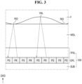
- FIG. 3 is an example diagram illustrating fingerprint detection by a display device according to one or more embodiments.
- the light output from the display pixels PX of the display panel 100 may be reflected from a ridge RID and a valley VAL of the fingerprint of the user's finger F.
- the ridge RID of the fingerprint is in contact with the cover window WDL, whereas the valley VAL of the fingerprint does not contact the cover window WDL. Therefore, the amount of light reflected from the ridge RID of the fingerprint and the amount of light reflected from the valley VAL may be different. That is, most of the light output from the display pixels PX of the display panel 100 is reflected from the ridge RID of the fingerprint, but hardly reflected from the valley VAL of the fingerprint.
- the light current of the optical element of a light sensing pixel PS may be different depending on whether the light is reflected from the ridge RID of the finger or the light is reflected from the valley VAL of the finger. Accordingly, the sensing current flowing to the sensing line RL may be different depending on whether the light is reflected from the ridge RID of the fingerprint of the finger F or the light is reflected from the valley VAL of the fingerprint of the finger F. Accordingly, the sensor driving circuit 300 detects the sensing voltages charged in the sensing lines RL by the sensing current, and thus the detected fingerprint pattern may be compared with a pre-stored fingerprint pattern. That is, fingerprint authentication may be possible using the display device 10.
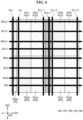
- FIG. 4 is an example diagram illustrating pixel driving units, sense driving units, scan write lines, scan initialization lines, scan control lines, light emitting lines, data lines, and sense lines according to one or more embodiments.
- FIG. 5 is a layout diagram illustrating display pixels and light sensing pixels in a display area of a display panel according to one or more embodiments.
- Each of the unit pixels UPX may include a first display pixel PX1, a second display pixel PX2, a third display pixel PX3, and a fourth display pixel PX4.
- the first display pixel PX1, the second display pixel PX2, the third display pixel PX3, and the fourth display pixel PX4 may be defined as a unit pixel UPX.
- the unit pixel UPX may be defined as the smallest unit of display pixels capable of displaying white.
- the first display pixel PX1 may include a first light emitting unit ELU1 that emits first light and a first pixel driving unit PDU1 that applies a driving current to the light emitting element of the first light emitting unit ELU1.
- the first light may be light of a red wavelength band.
- the main peak wavelength of the first light may be located at approximately 600 nm to 750 nm.
- the second display pixel PX2 may include a second light emitting unit ELU2 that emits second light and a second pixel driving unit PDU2 that applies a driving current to the light emitting element of the second light emitting unit ELU2.
- the second light may be light of a green wavelength band.
- the main peak wavelength of the second light may be located at approximately 480 nm to 560 nm.
- the third display pixel PX3 may include a third light emitting unit ELU3 that emits a third light and a third pixel driving unit PDU3 that applies a driving current to the light emitting device of the third light emitting unit ELU3.
- the third light may be light of a blue wavelength band.
- the main peak wavelength of the third light may be located at approximately 370 nm to 460 nm.
- the fourth display pixel PX4 may include a fourth light emitting unit ELU4 that emits the second light and a fourth pixel driving unit PDU4 that applies a driving current to the light emitting element of the fourth light emitting unit ELU4.
- the first pixel driving unit PDU1 and the second pixel driving unit PDU2 may be disposed in the first direction DR1
- the third pixel driving unit PDU3 and the fourth pixel driving unit PDU4 may be disposed in the first direction DR1.
- the first pixel driving unit PDU1 and the third pixel driving unit PDU3 may be disposed in the second direction DR2
- the second pixel driving unit PDU2 and the fourth pixel driving unit PDU4 may be disposed in the second direction DR2.
- the first light emitting unit ELU1 may overlap the first pixel driving unit PDU1 and the second pixel driving unit PDU2, and the third light emitting unit ELU3 may overlap the third pixel driving unit PDU3 and the third pixel driving unit PDU3.
- Each of the second light emitting unit ELU2 and the fourth light emitting unit ELU4 may overlap the first to fourth pixel driving units PDU1, PDU2, PDU3, and PDU4 and the light sensing units PSU.
- the first light emitting unit ELU1, the second light emitting unit ELU2, the third light emitting unit ELU3, and the fourth light emitting unit ELU4 may have an octagonal planar shape but are not limited thereto.
- the first light emitting unit ELU1, the second light emitting unit ELU2, the third light emitting unit ELU3, and the fourth light emitting unit ELU4 may have a rectangular planar shape such as a rhombus, or a polygonal planar shape other than a square and an octagon.
- Each of the light sensing pixels PS may include a light sensing unit PSU and a sensing driving unit PSDU.
- the light sensing unit PSU may be disposed between the first light-emitting unit ELU1 and the third light-emitting unit ELU3 adjacent in the first direction DR1, and may be disposed between the second light-emitting unit ELU2 and the fourth light-emitting unit ELU4 adjacent in the second direction DR2.
- the light sensing unit PSU may overlap the sensing driving unit PSDU.
- Each of the light sensing units PSU may have an octagonal planar shape but is not limited thereto.
- Each of the light sensing units PSU may have a rectangular planar shape such as a rhombus, or a polygonal planar shape other than a quadrangle and an octagon.
- a distance D12 between the center C1 of the first light emitting units ELU1 and the center C2 of the second light emitting units ELU2 adjacent to each other, a distance D23 between the center C2 of the second light emitting units ELU2 and the center C3 of the third light emitting unit ELU3 adjacent to each other, a distance D14 between the center C1 of the first light emitting unit ELU1 and the center C4 of the fourth light emitting unit ELU4 adjacent to each other, and a distance D34 between the center C3 of the third light emitting unit ELU3 and the center C4 of the fourth light emitting unit ELU4 adjacent to each other may be substantially the same.
- the scan write lines GWLk-1 and GWLk, the scan initialization lines GILk-1 and GILk, the scan control lines GCLk-1 and GCLk, and the light emitting lines EMI,k-1 and EMLk may be arranged in the direction DR1.
- the data lines DLj, DLj+1, DLj+2, and DLj+3 and the sensing lines RLq and RLq+1 may be arranged in the second direction DR2.
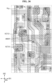
- Each of the sensing driving unit PSDU may overlap with one of the scan write lines GWLk-1 and GWLk, one of the scan initialization lines GILk-1 and GILk, one of the scan control lines GCLk-1 and GCLk, one of the light emitting lines EMI,k-1 and EMI,k, and one of the sensing lines RLq and RLq+1.
- Each of the first to fourth pixel driving units PDU1, PDU2, PDU3, and PDU4 may overlap with one of the scan write lines GWLk-1 and GWLk, one of the scan initialization lines GILk-1 and GILk, one of the scan control lines GCLk-1 and GCLk, one of the light emitting lines EMLk-1 and EMI,k, and one of the data lines DLj, DLj+1, DLj+2, DLj+3.
- the sensing driving unit PSDU may be disposed between the first pixel driving unit PDU1 and the fourth pixel driving unit PDU4 in the first direction DR1.
- the sensing driving unit PSDU and the pixel driving units PDU1, PDU2, PDU3, and PDU4 may be repeatedly arranged the sensing driving unit PSDU, the first pixel driving unit PDU1, the second pixel driving unit PDU2, the third pixel driving unit PDU3, and the fourth pixel driving unit PDU4 in the first direction DR1 in this order.
- the sensing driving unit PSDU may be disposed in the second direction DR2.
- the first pixel driving unit PDU1 and the third pixel driving unit PDU3 may be alternately disposed in the second direction DR2.
- the second pixel driving unit PDU2 and the fourth pixel driving unit PDU4 may be alternately disposed in the second direction DR2.
- FIG. 6 is an example diagram illustrating pixel driving units, sense driving units, scan write lines, scan initialization lines, scan control lines, light emitting lines, data lines, and sense lines according to another one or more embodiments.
- FIG. 7 is a layout diagram illustrating display pixels and light sensing pixels in a display area of a display panel according to another one or more embodiments.
- FIGS. 6 and 7 is different from the embodiment of FIGS. 4 and 5 in that the arrangement positions of the sensing driving unit PDU are changed.
- FIGS. 6 and 7 descriptions overlapping those of the embodiment of FIGS. 4 and 5 will be omitted.
- the sensing driving unit PSDU may be disposed between the first pixel driving unit PDU1 and the fourth pixel driving unit PDU4 in the first direction DR1 or between the second pixel driving unit PDU2 and the third pixel driving unit PDU3 in the first direction DR1.
- the sensing driving unit PSDU and the pixel driving units PDU1, PDU2, PDU3, and PDU4 may be repeatedly arranged the sensing driving unit PSDU, the first pixel driving unit PDU1, the second pixel driving unit PDU2, the sensing driving unit PSDU, the third pixel driving unit PDU3 and the fourth pixel driving unit PDU4 in the first direction DR1 in the order.
- FIG. 8 is an example diagram illustrating pixel driving units, sense driving units, scan write lines, scan initialization lines, scan control lines, light emitting lines, data lines, and sense lines according to another one or more embodiments.
- FIG. 9 is a layout diagram illustrating display pixels and light sensing pixels in a display area of a display panel according to another one or more embodiments.
- FIGS. 8 and 9 is different from the embodiment of FIGS. 6 and 7 in that empty spaces ES are disposed instead of some of the sensing driving units PDU.
- FIGS. 8 and 9 descriptions overlapping those of the embodiment of FIGS. 6 and 7 will be omitted.
- the empty spaces ES may be spaces in which the first to fourth pixel driving units PDU1, PDU2, PDU3, and PDU4 and the sensing driving unit PSDU are not disposed.
- the empty space ES may be disposed between the second pixel driving unit PDU2 and the third pixel driving unit PDU3 in the first direction DR1.
- the empty space ES may be disposed between the sensing driving unit PSDU adjacent to each other in the second direction DR2.
- the sensing driving unit PSDU may be surrounded by the second pixel driving unit PDU2, the third pixel driving unit PDU3, and the empty spaces ES.
- the sensing driving unit PSDU may be disposed between adjacent empty spaces ES in the second direction DR2.
- the sensing driving units PSDU, the pixel driving units PDU1, PDU2, PDU3, and PDU4, and the empty space ES may be repeatedly arranged the sensing driving unit PSDU, the first pixel driving unit PDU1, the second pixel driving unit PDU2, the empty space ES, the third pixel driving unit PDU3 and the fourth pixel driving unit PDU4 in the first direction DR1 in the order. Also, the sensing driving unit PSDU and the empty space ES may be repeatedly disposed in the second direction DR2.
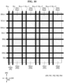
- FIG. 10 is an example diagram illustrating pixel driving units, sense driving units, scan write lines, scan initialization lines, scan control lines, light emitting lines, data lines, and sense lines according to another one or more embodiments.
- the embodiment of FIG. 10 is different from the embodiment of FIG. 4 in that the sensing driving unit PSDU are arranged to correspond to the pixel driving units PDU1, PDU2, PDU3, and PDU4 one-to-one.
- the sensing driving unit PSDU are arranged to correspond to the pixel driving units PDU1, PDU2, PDU3, and PDU4 one-to-one.
- FIG. 10 a description overlapping with the embodiment of FIG. 4 will be omitted.
- the sensing driving units PSDU may be disposed between adjacent pixel driving units PDU1, PDU2, PDU3, and PDU4 in the first direction DR1.
- the sensing driving unit PSDU may be disposed between the first pixel driving unit PDU1 and the second pixel driving unit PDU2 in the first direction DR1, between the second pixel driving unit PDU2 and the third pixel driving unit PDU3 in the first direction DR1, between the third pixel driving unit PDU3 and the fourth pixel driving unit PDU4 in the first direction DR1, and between the first pixel driving unit PDU1 and the fourth pixel driving unit PDU4 in the first direction DR1.
- the sensing driving unit PSDU and the pixel driving units PDU1, PDU2, PDU3, and PDU4 may be repeatedly arranged the sensing driving unit PSDU, the first pixel driving unit PDU1, the sensing driving unit PSDU, the second pixel driving unit PDU2, the sensing driving unit PSDU, the third pixel driving unit PDU3, the sensing driving unit PSDU, and the fourth pixel driving unit PDU4 in the first direction DR1 in the order.
- FIG. 11 is an example diagram illustrating pixel driving units, sense driving units, scan write lines, scan initialization lines, scan control lines, light emitting lines, data lines, and sense lines according to another one or more embodiments.
- FIG. 11 is different from the embodiment of FIG. 10 in that empty spaces ES are disposed instead of some of the sensing driving units PDU.
- FIG. 11 a description overlapping with the embodiment of FIG. 10 will be omitted.
- the empty spaces ES may be spaces in which the first to fourth pixel driving units PDU1, PDU2, PDU3, and PDU4 and the sensing driving unit PSDU are not disposed.
- the empty space ES may be disposed between the first pixel driving unit PDU1 and the second pixel driving unit PDU2 or between the third pixel driving unit PDU3 and the fourth pixel driving unit PDU4 in the first direction DR1.
- the empty space ES may be disposed between the sensing driving units PSDU adjacent to each other in the second direction DR2.
- the sensing driving unit PSDU may be surrounded by the second pixel driving unit PDU2, the third pixel driving unit PDU3, and the empty spaces ES.
- the sensing driving unit PSDU may be disposed between adjacent empty spaces ES in the second direction DR2.
- FIG. 12 is an example diagram illustrating pixel driving units, sense driving units, scan write lines, scan initialization lines, scan control lines, light emitting lines, data lines, and sense lines according to another one or more embodiments.
- the embodiment of FIG. 12 is different from the embodiment of FIG. 4 in that the sensing driving units PSDU are arranged to correspond to the pixel driving units DU1, PDU2, PDU3, and PDU4 one-to-one.
- the sensing driving units PSDU are arranged to correspond to the pixel driving units DU1, PDU2, PDU3, and PDU4 one-to-one.
- FIG. 12 a description overlapping with the embodiment of FIG. 4 will be omitted.
- the two sensing driving units PSDU may be disposed between the first pixel driving unit PDU1 and the fourth pixel driving unit PDU4 in the first direction DR1 or between the second pixel driving unit PDU2 and the third pixel driving unit PDU3 in the first direction DR1.
- the sensing driving units PSDU and the pixel driving units PDU1, PDU2, PDU3, and PDU4 may be repeatedly arranged the sensing driving unit PSDU, the first pixel driving unit PDU1, the second pixel driving unit PDU2, the sensing driving unit PSDU, the sensing driving unit PSDU, the third pixel driving unit PDU3, the fourth pixel driving unit PDU4, and the sensing driving unit PSDU in the first direction DR1 in the order.
- FIG. 13 is an example diagram illustrating pixel driving units, sense driving units, scan write lines, scan initialization lines, scan control lines, light emitting lines, data lines, and sense lines according to another one or more embodiments.
- FIG. 13 is different from the embodiment of FIG. 12 in that empty spaces ES are disposed instead of some of the sensing driving units PDU.
- FIG. 13 a description overlapping with the embodiment of FIG. 12 will be omitted.
- the empty spaces ES may be spaces in which the first to fourth pixel driving units PDU1, PDU2, PDU3, and PDU4 and the sensing driving unit PSDU are not disposed.
- the empty space ES may be disposed between the second pixel driving unit PDU2 and the third pixel driving unit PDU3 in the first direction DR1.
- the empty space ES may be disposed between the sensing driving units PSDU adjacent to each other in the second direction DR2.
- the sensing driving unit PSDU may be surrounded by the first pixel driving unit PDU1, the fourth pixel driving unit PDU4, and the empty spaces ES.
- the sensing driving unit PSDU may be disposed between adjacent empty spaces ES in the second direction DR2.
- the sensing driving units PSDU, the pixel driving units PDU1, PDU2, PDU3, and PDU4, and the empty spaces ES may be repeatedly arranged the sensing driving unit PSDU, the first pixel driving unit PDU1, the second pixel driving unit PDU2, the empty spaces ES, the third pixel driving unit PDU3, the fourth pixel driving unit PDU4, and the sensing driving unit PSDU in the first direction DR1 in the order. Also, the sensing driving unit PSDU and the empty space ES may be repeatedly disposed in the second direction DR2.
- the embodiment of FIG. 14 is different from the embodiment of FIG. 4 in that the area of the sensing driving unit PSDU is twice that of the sensing driving unit PSDU of the embodiment of FIG. 4 .
- a description overlapping with the embodiment of FIG. 4 will be omitted.
- the first sensing driving unit PSDU1 is disposed between the first pixel driving unit PDU1 and the fourth pixel driving unit PDU4 in the first direction DR1
- the second sensing driving unit PSDU2 is disposed between the second pixel driving unit PDU2 and the third pixel driving unit PDU3 in the first direction DR1.
- the sensing driving units PSDU and the pixel driving units PDU1, PDU2, PDU3, and PDU4 may be repeatedly arranged the sensing driving unit PSDU, the first pixel driving unit PDU1, the second pixel driving unit PDU2, the sensing driving unit PSDU, the third pixel driving unit PDU3, and the fourth pixel driving unit PDU4 in the first direction DR1 in the order.
- FIG. 15 is an example diagram illustrating pixel driving units, sense driving units, scan write lines, scan initialization lines, scan control lines, light emitting lines, data lines, and sense lines according to another one or more embodiments.
- FIG. 15 is different from the embodiment of FIG. 4 in that the sensing driving unit PSDU is disposed to correspond to one unit pixel UPX.
- the sensing driving unit PSDU is disposed to correspond to one unit pixel UPX.
- FIG. 15 a description overlapping with the embodiment of FIG. 4 will be omitted.
- the sensing driving units PSDU, the first pixel driving units PDU1, and the second pixel driving units PDU2 may be repeatedly arranged the sensing driving unit PSDU, the first pixel driving unit PDU1, and the second pixel driving unit PDU2 in the first direction DR1 in the order. That is, the sensing driving unit PSDU may be disposed on one side of the first pixel driving unit PDU1, and the second pixel driving unit PDU2 may be disposed on the other side of the first pixel driving unit PDU1.
- the sense driving units PSDU, the third pixel driving units PDU3, and the fourth pixel driving units PDU4 may be repeatedly arranged the sensing driving unit PSDU, the third pixel driving unit PDU3, and the second pixel driving unit PDU4 in the first direction DR1 in the order. That is, the sensing driving unit PSDU may be disposed on one side of the third pixel driving unit PDU3, and the fourth pixel driving unit PDU4 may be disposed on the other side of the third pixel driving unit PDU3.
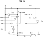
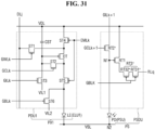
- FIG. 16 is a circuit diagram illustrating a display pixel and a light sensing pixel according to one or more embodiments.
- the first display pixel PX may be connected to the kth scan initialization line GILk, the kth scan write line GWLk, the kth scan control line GCLk, the kth scan bias line GBLk, and a jth data line DLj.
- the first display pixel PX may be connected to a first power suppy line VDL to which a first power voltage is supplied, a second power suppy line VSL to which a second power voltage is supplied, a first initialization line VIL1 to which the first initialization voltage is supplied, and the second initialization line VIL2 to which the second initialization voltage is supplied.
- the first display pixel PX may include the first light emitting unit ELU1 and the first pixel driving unit PDU1.
- the first light emitting unit ELU1 may include a light emitting element LE.
- the first pixel driving unit PDU1 may include a driving transistor DT, switch elements, and a capacitor CST.
- the switch elements include first to sixth transistors ST1, ST2, ST3, ST4, ST5, and ST6.
- the driving transistor DT may include a gate electrode, a first electrode, and a second electrode.
- the driving transistor DT controls a drain-source current (Isd, hereinafter referred to as a "driving current") flowing between the first electrode and the second electrode according to the data voltage applied to the gate electrode.
- the driving current Isd flowing through the channel of the driving transistor DT is the square of the difference between the voltage Vsg and the threshold voltage between the first electrode and the gate electrode of the driving transistor DT as shown in Eq. (1) proportional.
- Isd k ′ ⁇ Vsg ⁇ Vth 2
- Isd is a driving current, refers to a source-drain current flowing through the channel of the driving transistor DT, k' refers to a coefficient determined by the structure and physical characteristics of the driving transistor, Vsg refers to the voltage between the first electrode and the gate electrode of the driving transistor, and Vth refers to the threshold voltage of the driving transistor.
- a light emitting element LE emits light according to the driving current Isd. As the driving current Isd increases, the amount of light emitted from the light emitting element LE may increase.
- the light emitting element LE may be an organic light emitting diode including an organic light emitting layer disposed between an anode electrode and a cathode electrode.
- the light emitting element LE may be a quantum dot light emitting element including a quantum dot light emitting layer disposed between the anode electrode and the cathode electrode.
- the light emitting element LE may be an inorganic light emitting element including an inorganic semiconductor disposed between the anode electrode and the cathode electrode.
- the light emitting element LE is an inorganic light emitting element, it may include a micro light emitting diode or a nano light emitting diode.
- the anode electrode of the light emitting element LE may be connected to the second electrode of the fifth transistor ST5 and the first electrode of the sixth transistor ST6, and the cathode electrode may be connected to a second power supply line VSL.
- the first transistor ST1 is turned-on by the kth scan write signal of the kth scan write line GWLk to connect the first electrode of the driving transistor DT to the jth data line Dj. Accordingly, the data voltage of the jth data line DLj may be applied to the first electrode of the driving transistor DT.
- the gate electrode of the first transistor ST1 may be connected to the kth scan write line GWLk, the first electrode may be connected to the first electrode of the driving transistor DT, and the second electrode may be connected to the jth data line DLj.
- the second transistor ST2 is turned-on by the kth scan control signal of the kth scan control line GCLk to connect the gate electrode and the second electrode of the driving transistor DT.
- the driving transistor DT is driven as a diode.
- the gate electrode of the second transistor ST2 may be connected to the kth scan control line GCLk, the first electrode may be connected to the gate electrode of the driving transistor DT, and the second electrode may be connected to the second electrode of the driving transistor DT.
- the third transistor ST3 is turned-on by the kth scan initialization signal of the kth scan initialization line GILk to connect the gate electrode of the driving transistor DT to a first initialization voltage line VIL1. Accordingly, the first initialization voltage VINT1 of the first initialization voltage line VIL1 may be applied to the gate electrode of the driving transistor DT.
- the gate electrode of the third transistor ST3 may be connected to the kth scan initialization line GILk, the first electrode may be connected to the first initialization voltage line VIL1, and the second electrode may be connected to the gate electrode of the driving transistor DT.
- the fourth transistor ST4 is turned-on by the kth light emitting signal of the kth light emitting line EMI,k to connect the first electrode of the driving transistor DT to the first power supply line VDL.
- the gate electrode of the fourth transistor ST4 may be connected to the kth light emitting line EMI,k, the first electrode may be connected to the first power supply line VDL, and the second electrode may be connected to the first electrode of the driving transistor DT.
- the fifth transistor ST5 is turned-on by the kth light emitting signal of the kth light emitting line EMI,k to connect the second electrode of the driving transistor DT to the anode electrode of the light emitting element LE.
- the gate electrode of the fifth transistor ST5 may be connected to the kth light emitting line EMI,k, the first electrode may be connected to the second electrode of the driving transistor DT, and the second electrode may be connected to the anode electrode of the light emitting element LE.
- the driving current Isd of the driving transistor DT may flow through the light emitting element LE.
- the sixth transistor ST6 is turned-on by the kth scan bias signal of the kth scan bias line GBLk to connect the anode electrode of the light emitting element LE to a second initialization voltage line VIL2.
- the second initialization voltage VINT2 of the second initialization voltage line VIL2 may be applied to the anode electrode of the light emitting element LE.
- the gate electrode of the sixth transistor ST6 may be connected to the kth scan bias line GBLk, the first electrode may be connected to the anode electrode of the light emitting element LE, and the second electrode may be connected to the second initialization voltage line VIL2.
- the capacitor CST is formed between the gate electrode of the driving transistor DT and the first power suppy line VDL.
- the first capacitor electrode of the capacitor CST may be connected to the gate electrode of the driving transistor DT, and the second capacitor electrode may be connected to the first power supply line VDL.
- the second electrode may be a drain electrode.
- the first electrode of each of the driving transistor DT and the first to sixth transistors ST1, ST2, ST3, ST4, ST5, and ST6 is the drain electrode, the second electrode may be a source electrode.
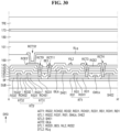
- the driving transistor DT and an active layer of each of the first to sixth transistors ST1, ST2, ST3, ST4, ST5, and ST6 may be formed of any one of polysilicon, amorphous silicon, and oxide semiconductor.
- the active layer of each of the driving transistor DT, the first transistor ST1, and the fourth to sixth transistors ST4 to ST6 may be made of polysilicon.
- Each active layer of the second transistor ST2 and the third transistor ST3 may be made of an oxide semiconductor.
- the driving transistor DT, the first transistor ST1, and the fourth to sixth transistors ST4 to ST6 may be formed of a P-type MOSFET, and the second transistor ST2 and the third transistor ST3 may be formed of an N-type MOSFET.
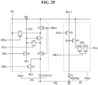
- the light sensing pixel PS may be connected to the kth scan initialization line GILk-1, the kth scan initialization line GILk, and the kth scan control line GCLk. Also, the light sensing pixel PS may be connected to a second power supply line VSL to which a second power voltage is supplied.
- the light sensing pixel PS may include a light sensing unit PSU and a sensing driving unit PSDU.
- the light sensing unit PSU may include an optical element PD.
- the sensing driving unit PSDU may include first to third sensing transistors RT1 to RT3.
- the optical element PD may be a photodiode including the anode electrode, a photoelectric conversion layer, and the cathode electrode.
- the anode electrode of the optical element PD may be connected to a first node N1, and the cathode electrode may be connected to the second power supply line VSL.
- the optical element PD may convert incident light into an electrical signal. When light is incident on the optical element PD, a photocurrent flowing through the optical element PD may increase compared to when light is not incident on the optical element PD.
- An optical device PD may be an organic photodiode including an electron donating material generating donor ions and an electron accepting material generating acceptor ions.
- the optical element PD When the optical element PD is exposed to light, photocharges may be generated, and the generated photocharges may be accumulated in the anode electrode of the optical element PD. Therefore, when the optical element PD is exposed to light, the voltage of the first node N1 connected to the anode electrode of the optical element PD may increase.
- a first sensing transistor RT1 is turned-on by the voltage of the first node N1 applied to the gate electrode to connect the first power supply line VDL to the second electrode of a third sensing transistor RT3.
- the gate electrode of the first sensing transistor RT1 may be connected to the first node N1, the first electrode may be connected to the first power supply line VDL, and the second electrode may be connected to the second electrode of the third sensing transistor RT3.
- a second sensing transistor RT2 is turned-on by the kth scan control signal of the kth scan control line GCLk to connect a k-1th scan initialization line GILk-1 to the first node N1.
- the gate electrode of the second sensing transistor RT2 may be connected to the kth scan control line GCLk, the first electrode may be connected to the k-1th scan initialization line GILk-1, and the second electrode may be connected to the first node N1.
- the third sensing transistor RT3 is turned-on by the kth scan initialization signal of the kth scan initialization line GILk to connect the second electrode of the first sensing transistor RT1 to the qth sensing line RLq. Accordingly, the sensing current of the first sensing transistor RT1 may flow to the qth sensing line RLq.
- the gate electrode of the third sensing transistor RT3 may be connected to the kth scan initialization line GILk, the first electrode may be connected to the qth sensing line RLq, and the second electrode may be connected to the second electrode of the first sensing transistor RT1.
- the second electrode may be a drain electrode.
- the second electrode may be a source electrode.
- An active layer of each of the first to third sensing transistors RT1, RT2, and RT3 may be formed of any one of polysilicon, amorphous silicon, and oxide semiconductor.
- the active layer of the first sensing transistor RT1 may be made of polysilicon.
- Each active layer of the second sensing transistor RT2 and the third sensing transistor RT3 may be formed of an oxide semiconductor.
- the first sensing transistor RT1 may be formed of a P-type MOSFET
- the second sensing transistor RT2 and the third sensing transistor RT3 may be formed of an N-type MOSFET.
- the circuit diagram of the second pixel driving unit PDU2 of the second display pixel PX2, the third pixel driving unit PDU3 of the third display pixel PX3, and the fourth pixel driving unit PDU4 of the fourth display pixel PX4 may be substantially the same as the circuit diagram of the first pixel driving unit PDU1 of the first display pixel PX1 described in connection with FIG. 16 . Therefore, the description the circuit diagram of the second pixel driving unit PDU2 of the second display pixel PX2, the third pixel driving unit PDU3 of the third display pixel PX3, and the fourth pixel driving unit PDU4 of the fourth display pixel PX4 will be omitted.
- the fingerprint sensing ability may be deteriorated due to the off-leakage current of the second sensing transistor RT2 and the off-leakage current of the third sensing transistor RT3 are used.
- the second sensing transistor RT2 and the third sensing transistor RT3 may be formed of an N-type MOSFET in the embodiment of the present specification without additional process. Therefore, it is possible to reduce the deterioration of the fingerprint sensing ability due to the off-leakage current of the second sensing transistor RT2 and the off-leakage current of the third sensing transistor RT3 by forming the second sensing transistor RT2 and the third sensing transistor RT3 with N-type MOSFET.
- the first pixel driving unit PDU1 and the sensing driving unit PSDU share the kth scan control line GCLk, the kth scan initialization line GILk, the (k-1)th scan initialization line GILk-1, the second initialization line VIL2, and the second power supply line VSL. Therefore, although the sensing driving unit PSDU is added, there is an advantage in that a separate wire to which a separate signal for driving the sensing driving unit PSDU is applied is not required.
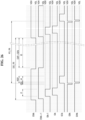
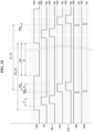
- FIG. 17 is a waveform diagram illustrating a (k-1)th scan initialization signal, a kth scan initialization signal, a kth scan control signal, a kth scan write signal, a kth scan bias signal, and a k th light emitting signal applied to a display pixel and a light sensing pixel according to one or more embodiments.
- a kth light emitting signal EMk is a signal applied to a kth light emitting line EMI,k, and is a signal for controlling turn-on and turn-off of the fourth transistor ST4 and the fifth transistor ST5.
- a kth scan initialization signal GIk is a signal applied to the kth scan initialization line GILk, and is a signal for controlling turn-on and turn-off of the third transistor ST3 and the third sensing transistor RT3.
- a kth scan control signal GCk is a signal applied to the kth scan control line GCLk, and is a signal for controlling turn-on and turn-off of the second transistor ST2 and the second sensing transistor RT2.
- a kth scan write signal GWk is applied to the kth scan write line GWLk and is a signal for controlling turn-on and turn-off of the first transistor ST1.
- a kth scan bias signal GBk is applied to the kth scan bias line GBLk and is a signal for controlling turn-on and turn-off of the sixth transistor ST6.
- the kth scan initialization signal GIk, the kth scan control signal GCk, the kth scan write signal GWk, the kth scan bias signal GBk, and the kth light emitting signal EMk may be repeated in one frame period DIS_FR and PS_FR.
- the first frame period DIS_FR1 may include a first period t1 for initializing the voltage of the gate electrode of the driving transistor DT to the first initialization voltage VINT1, a second period t2 for initializing the voltage of the anode electrode of the light emitting element LE to the second initialization voltage VINT2, a third period t3 for supplying the data voltage to the first electrode of the driving transistor DT, and a fourth period t4 for sampling the threshold voltage of the driving transistor DT based on the operation of the first display pixel PX1 and based on the operation of the display pixel PX.
- the kth scan initialization signal GIk may have a second level voltage VGH during the first period t1 and may have a first level voltage VGL during the remaining period.
- the kth scan bias signal GBk may have the first level voltage VGL during the second period t2 and may have the second level voltage VGH during the remaining period.
- the kth scan control signal GCk may have the second level voltage VGH during the third period t3 and the fourth period t4 and may have the first level voltage VGL during the remaining period.
- the kth scan write signal GWk may have the first level voltage VGL during the third period t3 and the second level voltage VGH during the remaining period.
- the kth emitting signal EMk may have the second level voltage VGH during the first to fourth periods t1 to t4 and may have the first level voltage VGL during the fifth period t5.
- the first level voltage VGL may be a gate low voltage
- the second level voltage VGH may be a gate high voltage.
- the kth scan write signal GWk having the first level voltage VGL is supplied to the kth scan write line GWLk
- the kth scan control signal GCk having the second level voltage VGH is supplied to the kth scan control line GCLk.
- the first transistor ST1 is turned-on by the kth scan write line GWLk having the first level voltage VGL
- the second transistor ST2 is turned-on by the kth scan control line GCLk having the second level voltage VGH. Due to the turn-on of the first transistor ST1, the data voltage of the jth data line DLj is supplied to the first electrode of the driving transistor DT.
- the kth scan control signal GCk having the second level voltage VGH is supplied to the kth scan control line GCLk.
- the second transistor ST2 is turned-on by the kth scan control line GCLk having the second level voltage VGH. Due to the turn-on of the second transistor ST2, the gate electrode and the second electrode of the driving transistor DT are connected to each other, and the driving transistor DT is driven by a diode.
- the kth light emitting signal EMk having the first level voltage VGL is supplied to the kth light emitting line EMI,k.
- the fourth transistor ST4 and the fifth transistor ST5 may be turned-on by the kth emitting signal EMk having the first level voltage VGL. Due to the turn-on of the fourth transistor ST4, the first electrode of the driving transistor DT may be connected to the first power supply line VDL. Due to the turn-on of the fifth transistor ST5, the second electrode of the driving transistor DT may be connected to the anode electrode of the light emitting element LE.
- the driving current Isd may be supplied to the light emitting element LE.
- Vth is the threshold voltage of the driving transistor DT
- VDD is the first power voltage of the first power supply line VDL
- Vdata is the data voltage.
- the gate voltage of the driving transistor DT is (Vdata-Vth), and the voltage of the first electrode is VDD.
- one frame period PS_FR1 may include a reset period RSP for resetting the first node N1, a light exposure period EXP for exposing the optical element PD to light, and a sensing period SEN for sensing a sensing current flowing through the qth sensing line RLq according to the voltage of the first node N1.
- the kth scan control signal GCk may have the second level voltage VGH during the reset period RSP and the first level voltage VGL during the light exposure period EXP and the sensing period SEN.
- the kth scan initialization signal GIk may have the second level voltage VGH during the sensing period SEN and may have the first level voltage VGL during the reset period RSP and the light exposure period EXP.
- the kth scan control signal GCk having the second level voltage VGH is supplied to the kth scan control line GCLk.
- the second sensing transistor RT2 is turned-on by the kth scan control signal GCk having the second level voltage VGH. Due to the turn-on of the second sensing transistor RT2, the first node N1 may be connected to the k-1th scan initialization line GILk-1. Therefore, the first level voltage VGL of the k-1th scan initialization line GILk-1 may be supplied to the first node N1 during the reset period RSP. Since the first level voltage VGL has a lower potential than the second power voltage VSS, the optical element PD may have a reverse bias state.
- the light exposure period EXP During the light exposure period EXP, light emitted from the light emitting element LE may be reflected from the fingerprint of the finger F to be incident on the optical element PD. Accordingly, when light is incident on the optical element PD, photocharges may be generated, and the generated photocharges may be accumulated in the anode electrode of the optical element PD. Accordingly, the voltage of the first node N1 may increase. Since the voltage of the first node N1 increases as the amount of charge accumulated in the first node N1 increases, the light exposure period EXP is preferably set to be sufficiently long.
- the kth scan initialization signal GIk having the second level voltage VGH is supplied to the kth scan initialization line GILk.
- the third sensing transistor RT3 is turned-on by the kth scan initialization signal GIk having the second level voltage VGH. Due to the turn-on of the third sensing transistor RT3, the sensing current of the first sensing transistor RT1 according to the voltage of the first node N1 may flow to the qth sensing line RLq.
- the sensor driving circuit 300 senses the sensing voltage charged in the qth sensing line RLq by the sensing current, whereby the detected fingerprint pattern may be compared with a previously stored fingerprint pattern. That is, fingerprint authentication may be possible using the display device 10.
- FIG. 18 is a layout diagram illustrating a first active layer, a first gate layer, a second gate layer, a second active layer, a third gate layer, and a first source drain layer of the first sub-pixel and the light sensing pixel according to one or more embodiments.
- FIG. 19 is a layout diagram illustrating a first active layer, a first gate layer, a second gate layer, a second active layer, a third gate layer, a first source drain layer, and a second source drain layer of the first sub-pixel and the light sensing pixel according to one or more embodiments.
- the first pixel driving unit PDU1 may include a driving transistor DT, first to sixth transistors ST1 to ST6, a capacitor CST, connection electrodes BE1 to BE6, and a first anode connection electrode ANDE1.
- the driving transistor DT may include a channel layer DTCH, a gate electrode DTG, a first electrode DTS, and a second electrode DTD.
- the channel layer DTCH of the driving transistor DT may overlap the gate electrode DTG of the driving transistor DT.
- the gate electrode DTG of the driving transistor DT may be disposed on the channel layer DTCH of the driving transistor DT.
- the gate electrode DTG of the driving transistor DT may be connected to a first connection electrode BE1 through a first connection contact hole BCNT1.
- the first connection electrode BE1 may be connected to a second electrode D2 of the second transistor ST2 through a second connection contact hole BCNT2.
- the first connection electrode BE1 may cross the kth scan control line GCLk.
- the second electrode DTD of the driving transistor DT may be connected to a second connection electrode BE2 through a third connection contact hole BCNT3.
- the second connection electrode BE2 may be connected to a first electrode S2 of the second transistor ST2 through a fourth connection contact hole BCNT4.
- the first transistor ST1 may be connected to a channel layer CH1, a gate electrode G1, the first electrode S1, and a second electrode D1.
- the channel layer CH1 of the first transistor ST1 may overlap the gate electrode G1 of the first transistor ST1.
- the gate electrode G1 of the first transistor ST1 may be disposed on the channel layer CH1 of the first transistor ST1.
- the gate electrode G1 of the first transistor ST1 may be integrally formed with the kth scan write line GWLk.
- the gate electrode G1 of the first transistor ST1 may be a part of the kth scan write line GWLk.
- the first electrode S1 of the first transistor ST1 may be connected to the first electrode DTS of the driving transistor DT.
- the first electrode S1 of the first transistor ST1 may be extended in the second direction DR2, and thus the first electrode S1 of the first transistor ST1 may overlap the kth scan control line GCLk, a first shielding electrode SHE1, the second initialization voltage line VIL2, the second electrode RD2 of the second sensing transistor RT2, and the first sensing connection electrode RCE1.
- the first shielding electrode SHE1 may be extended in the first direction DR1 and may overlap the kth scan control line GCLk.
- the second electrode D1 of the first transistor ST1 may be connected to a third connection electrode BE3 through a fifth connection contact hole BCNT5.
- the third connection electrode BE3 may be connected to the jth data line DLj through a sixth connection contact hole BCNT6.
- the second transistor ST2 may be connected to a channel layer CH2, a gate electrode G2, a first electrode S2, and a second electrode D2.
- the channel layer CH2 of the second transistor ST2 may overlap the gate electrode G2 of the second transistor ST2.
- the gate electrode G2 of the second transistor ST2 may be disposed on the channel layer CH2 of the second transistor ST2.
- the gate electrode G2 of the second transistor ST2 may be integrally formed with the kth scan control line GCLk.
- the gate electrode G2 of the second transistor ST2 may be a part of the kth scan control line GCLk.
- the first electrode S2 of the second transistor ST2 may be connected to the second connection electrode BE2 through the fourth connection contact hole BCNT4.
- the second electrode D2 of the second transistor ST2 may be connected to the first connection electrode BE1 through the second connection contact hole BCNT2.
- the second electrode D2 of the second transistor ST2 may be connected to a second electrode D3 of the third transistor ST3.
- the first electrode S3 of the third transistor ST3 may be connected to a fourth connection electrode BE4 through a seventh connection contact hole BCNT7.
- the fourth connection electrode BE4 may be connected to the first initialization voltage line VIL1 through an eighth connection contact hole BCNT8.
- the second electrode D3 of the third transistor ST3 may be connected to the second electrode D2 of the second transistor ST2.
- the fourth transistor ST4 may be connected to a channel layer CH4, a gate electrode G4, a first electrode S4, and a second electrode D4.
- the channel layer CH4 of the fourth transistor ST4 may overlap the gate electrode G4 of the fourth transistor ST4.
- the gate electrode G4 of the fourth transistor ST4 may be disposed on the channel layer CH4 of the fourth transistor ST4.
- the gate electrode G4 of the fourth transistor ST4 may be integrally formed with the kth light emitting line EMLk.
- the gate electrode G4 of the fourth transistor ST4 may be a part of the kth light emitting line EMI,k.
- the first electrode S4 of the fourth transistor ST4 may be connected to a fifth connection electrode BE5 through a ninth connection contact hole BCNT9.
- the fifth connection electrode BE5 may be connected to the first power supply line VDL through a tenth connection contact hole BCNT10.
- the second electrode D2 of the fourth transistor ST4 may be connected to the first electrode DTS of the driving transistor DT and the first electrode S1 of the first transistor ST1.
- the fifth transistor ST5 may be connected to a channel layer CH5, a gate electrode G5, a first electrode S5, and a second electrode D5.
- the channel layer CH5 of the fifth transistor ST5 may overlap the gate electrode G5 of the fifth transistor ST5.
- the gate electrode G5 of the fifth transistor ST5 may be disposed on the channel layer CH5 of the fifth transistor ST5.
- the gate electrode G5 of the fifth transistor ST5 may be integrally formed with the kth light emitting line EMI,k.
- the gate electrode G5 of the fifth transistor ST5 may be a part of the kth light emitting line EMLk.
- the first electrode S5 of the fifth transistor ST5 may be connected to the second connection electrode BE2 through the third connection contact hole BCNT3.
- the second electrode D5 of the fifth transistor ST5 may be connected to a sixth connection electrode BE6 through an eleventh connection contact hole BCNT11.
- the sixth connection electrode BE6 may be connected to the first anode connection electrode ANDE1 through a twelfth connection contact hole BCNT12.
- the first electrode of the light emitting element LE may be connected to the first anode connection electrode ANDE1 through a first anode contact hole.
- the first electrode S6 of the sixth transistor ST6 may be connected to the sixth connection electrode BE6 through a thirteenth connection contact hole BCNT13.
- the first electrode S6 of the sixth transistor ST6 may overlap the kth scan initialization line GILk and a second shielding electrode SHE2.
- the second electrode D6 of the sixth transistor ST6 may be connected to the second initialization voltage line VIL2 through the thirteenth connection contact hole BCNT13.
- the second shielding electrode SHE2 may be extended in the first direction DR1 and may overlap the kth scan initialization line GILk.
- a first electrode CE11 of the capacitor CST may be integrally formed with the gate electrode DTG of the driving transistor DT.
- the first electrode CE11 of the capacitor CST may be a part of the gate electrode DTG of the driving transistor DT.
- a second electrode CE12 of the capacitor CST may overlap the first electrode CE11 of the capacitor CST.
- the second electrode CE12 of the capacitor CST may be connected to the fifth connection electrode BE5 through a fourteenth connection contact hole BCNT14.
- the first sensing transistor RT1 may be connected to a channel layer RCH1, a gate electrode RG1, a first electrode RS1, and a second electrode RD1.
- the channel layer RCH1 of the first sensing transistor RT1 may overlap the gate electrode RG1 of the first sensing transistor RT1.
- the gate electrode RG1 of the first sensing transistor RT1 may be disposed on the channel layer RCH1 of the first sensing transistor RT1.
- the gate electrode RG1 of the first sensing transistor RT1 may be connected to a first sensing connection electrode RCE1 through a first sensing contact hole RCT1.
- the first sensing connection electrode RCE1 may be connected to a first electrode RS2 of the second sensing transistor RT2 through a second sensing contact hole RCT2.
- the first sensing connection electrode RCE1 may be connected to the second anode connection electrode ANDE2 through a twelfth sensing contact hole RCT12.
- a first electrode of the optical element PD may be connected to the second anode connection electrode ANDE2 through a second anode contact hole.
- the first electrode RS 1 of the first sensing transistor RT1 may be connected to the fifth connection electrode BE5 through an eleventh sensing contact hole RCT11.
- the first electrode RS1 of the first sensing transistor RT1 may be extended in the second direction DR2, and may overlap the second initialization voltage line VIL2, the kth scan control line GCLk, and the first shielding electrode SHE1.
- the second electrode RD1 of the first sensing transistor RT1 may be connected to a second sensing connection electrode RCE2 through a third sensing contact hole RCT3.
- the second sensing connection electrode RCE2 may be connected to a first electrode RS3 of the third sensing transistor RT3 through a fourth sensing contact hole RCT4.
- the second sensing transistor RT2 may be connected to a channel layer RCH2, a gate electrode RG2, a first electrode RS2, and a second electrode RD2.
- the channel layer RCH2 of the second sensing transistor RT2 may overlap the gate electrode RG2 of the second sensing transistor RT2.
- the gate electrode RG2 of the second sensing transistor RT2 may be disposed on the channel layer RCH2 of the second sensing transistor RT2.
- the gate electrode RG2 of the second sensing transistor RT2 may be integrally formed with the kth scan control line GCLk.
- the gate electrode RG2 of the second sensing transistor RT2 may be a part of the kth scan control line GCLk.
- the first electrode RS2 of the second sensing transistor RT2 may overlap the second initialization voltage line VIL2.
- the first electrode RS2 of the second sensing transistor RT2 may be connected to a third sensing connection electrode RCE3 through a fifth sensing contact hole RCT50.
- the third sensing connection electrode RCE3 may be connected to an initialization connection electrode VIE through a sixth sensing contact hole RCT6.
- the initialization connection electrode VIE may be connected to a fourth sensing connection electrode RCE4 through a seventh sensing contact hole RCT7.
- the fourth sensing connection electrode RCE4 may be connected to the k-1th scan initialization line GILk-1 through an eighth sensing contact hole RCT8.
- the second electrode RD2 of the second sensing transistor RT2 may be connected to the first sensing connection electrode RCE1 through the second sensing contact hole RCT2.
- the initialization connection electrode VIE may be extended long in the second direction DR2, it may be disposed in the sensing driving unit PSDU disposed in the (k-1)th row and the kth row. Accordingly, the first electrode RS2 of the second sensing transistor RT2 disposed in the sensing driving unit PSDU of the kth row may be connected to the k-1th scan initialization line GILk-1. In addition, when the initialization connection electrode VIE is disposed in the sensing driving unit PSDU disposed in the kth row and the (k+1)th row, the first electrode RS2 of the second sensing transistor RT2 disposed in the sensing driving unit PSDU of the (k+1)th row may be connected to the kth scan initialization line GILk.
- the sensing driving unit PSDU disposed in the kth row refers to the sensing driving unit PSDU overlapping the kth scan write line GWLk, the kth scan initialization line GILk, the kth scan control line GCLk, and the kth light emitting line EMI,k.
- the third sensing transistor RT3 may be connected to a channel layer RCH3, a gate electrode RG3, a first electrode RS3, and a second electrode RD3.
- the channel layer RCH3 of the third sensing transistor RT3 may overlap the gate electrode RG3 of the third sensing transistor RT3.
- the gate electrode RG3 of the third sensing transistor RT3 may be disposed on the channel layer RCH3 of the third sensing transistor RT3.
- the gate electrode RG3 of the third sensing transistor RT3 may be integrally formed with the kth scan initialization line GILk.
- the gate electrode RG3 of the third sensing transistor RT3 may be a part of the kth scan initialization line GILk.
- the first electrode RS3 of the third sensing transistor RT3 may be connected to the second sensing connection electrode RCE2 through the fourth sensing contact hole RCT4.
- the second electrode RD3 of the third sensing transistor RT3 may be connected to a fifth sensing connection electrode RCE5 through a ninth sensing contact hole RCT9.
- the fifth sensing connection electrode RCE5 may be connected to the qth sensing line RLq through a tenth sensing contact hole RCT10.
- the second pixel driving unit PDU2 the third pixel driving unit PDU3, and the fourth pixel driving unit PDU4 are substantially the same as the first pixel driving unit PDU1 described with reference to FIGS. 18 and 19 , a description of these will be omitted.
- FIG. 20 is a cross-sectional view illustrating an example of the display panel taken along line A-A' of FIGS. 18 and 19 .
- FIG. 21 is a cross-sectional view illustrating an example of the display panel taken along lines B-B' and C-C' of FIGS. 18 and 19 .
- FIG. 22 is a cross-sectional view illustrating an example of the display panel taken along line D-D' of FIGS. 18 and 19 .
- FIG. 23 is a cross-sectional view illustrating an example of the display panel taken along line E-E' of FIGS. 18 and 19 .
- FIG. 24 is a cross-sectional view illustrating an example of the display panel taken along line F-F' of FIGS. 18 and 19 .
- a display layer DPL and the encapsulation layer TFE may be sequentially formed on the substrate SUB.
- the display layer DPL may include a thin film transistor layer TFTL and a light emitting element layer EML.
- the thin film transistor layer TFTL may be a layer in which the driving transistor DT, the first to sixth transistors ST1 to ST6, and the capacitor CST of each of the pixel driving units PDU1 to PDU4 and a layer in which the first to third sensing transistors RT1 to RT3 of each of the sensing driving units PSDU are formed.
- the thin film transistor layer TFTL includes a first active layer ACT1, a second active layer ACT2, a first gate layer GTL1, a second gate layer GTL2, a third gate layer GTL3, a first data metal layer DTL1, a second data metal layer DTL2, a buffer layer BF, a first gate insulating layer 131, a second gate insulating layer 132, a first interlayer insulating layer 141, a second interlayer insulating layer 142, a third interlayer insulating layer 143, a first organic layer 160, and a second organic layer 161.
- a buffer layer BF may be disposed on one surface of the substrate SUB.
- the buffer layer BF may be formed on one surface of the substrate SUB to protect the thin film transistors and an organic light emitting layer 172 of the light emitting element layer EML from moisture penetrating through the substrate SUB, which is vulnerable to moisture permeation.
- the buffer layer BF may be made of a plurality of inorganic layers alternately stacked.
- the buffer layer BF may be formed as a multilayer in which one or more inorganic layers of a silicon nitride layer, a silicon oxynitride layer, a silicon oxide layer, a titanium oxide layer, and an aluminum oxide layer are alternately stacked.
- the buffer layer BF may be omitted.
- the first active layer ACT1 may be disposed on the buffer layer BF.
- the first active layer ACT1 may include a silicon semiconductor such as polycrystalline silicon, single crystal silicon, low-temperature polycrystalline silicon, and amorphous silicon.
- the first active layer ACT1 may include a channel layer DTCH of the driving transistor DT, a first electrode DTS, and a second electrode DTD.
- the channel layer DTCH of the driving transistor DT may be an area overlapping the gate electrode DTG of the driving transistor DT in the third direction DR3, which is a thickness direction of the substrate SUB.
- the first electrode DTS of the driving transistor DT may be disposed on one side of the channel layer DTCH, and the second electrode DTD may be disposed on the other side of the channel layer DTCH.
- the first electrode DTS and the second electrode DTD of the driving transistor DT may be areas that do not overlap the gate electrode DTG in the third direction DR3.
- the first electrode DTS and the second electrode DTD of the driving transistor DT may be areas having conductivity by doping the silicon semiconductor with ions or impurities.
- the first active layer ACT1 may further include the channel layers CH1 and CH4 to CH6, the first electrodes S1 and S4 to S6, and second electrodes D1 and D4 to D6 of the first and fourth to sixth transistors ST1 and ST4 to ST6.
- Each of the channel layers CH1 and CH4 to CH6 of the first and fourth to sixth transistors ST1 and ST4 to ST6 may be overlapped with a corresponding gate electrode among the gate electrodes G1 and G4 to G6 in the third direction DR3.
- the first electrodes S1 and S4 to S6 and the second electrodes D1 and D4 to D6 of the first and fourth to sixth transistors ST1 to ST6 may be areas having conductivity by doping the silicon semiconductor with ions or impurities.
- the first active layer ACT1 may further include the channel layer RCH1, the first electrode RS1, and the second electrode RD1 of the first sensing transistor RT1.
- the channel layer RCH1 of the first sensing transistor RT1 may overlap the gate electrode RG1 in the third direction DR3.
- the first electrode RS1 and the second electrode RD1 of the first sensing transistor RT1 may be areas having conductivity by doping the silicon semiconductor with ions or impurities.
- the first gate insulating layer 131 may be disposed on the first active layer ACT1.
- the first gate insulating layer 131 may be formed of an inorganic layer, for example, a silicon nitride layer, a silicon oxynitride layer, a silicon oxide layer, a titanium oxide layer, or an aluminum oxide layer.
- a first gate layer GTL1 may be disposed on the first gate insulating layer 131.
- the first gate layer GTL1 may include the gate electrode DTG of the driving transistor DT.
- the first gate layer GTL1 may further include the gate electrodes G1 to G6 of the first to sixth transistors ST1 to ST6, the first capacitor electrode CE11, the scan write lines GWLk and the light emitting line Elk.
- the first gate layer GTL1 may further include gate electrodes RG1 to RG3 of the first to third sensing transistors RT1 to RT3.
- the first interlayer insulating layer 141 may be disposed on the first gate layer GTL1.
- the first interlayer insulating layer 141 may be formed of the inorganic layer, for example, the silicon nitride layer, the silicon oxynitride layer, the silicon oxide layer, the titanium oxide layer, or the aluminum oxide layer.
- the second gate layer GTL2 may be disposed on the first interlayer insulating layer 141.
- the second gate layer GTL2 may include a second capacitor electrode CE12, shielding electrodes SHE1 and SHE2, and the first initialization voltage line VIL1.
- the second gate metal layer may be formed as a single layer or multiple layers made of at least one of molybdenum (Mo), aluminum (Al), chromium (Cr), gold (Au), titanium (Ti), nickel (Ni), neodymium (Nd) and copper (Cu) or an alloy thereof.
- the second interlayer insulating layer 142 may be disposed on the second gate layer GTL2.
- the second interlayer insulating layer 142 may be formed of an inorganic layer, for example, a silicon nitride layer, a silicon oxynitride layer, a silicon oxide layer, a titanium oxide layer, or an aluminum oxide layer.
- the second active layer ACT2 may be disposed on the second interlayer insulating layer 142.
- the second active layer ACT2 may include oxide semiconductors such as IGZO (indium (In), gallium (Ga), zinc (Zn) and oxygen (O)), IGZTO (indium (In), gallium (Ga), zinc (Zn), tin (Sn) and oxygen (O)), or IGTO (indium (In), gallium (Ga), tin (Sn) and oxygen (O)).
- the second active layer ACT2 may further include the channel layers CH2 and CH3, the first electrodes S2 and S3, and the second electrodes D2 and D3 of the second and third transistors ST2 and ST3.
- Each of the channel layers CH2 and CH3 of the second and third transistors ST2 and ST3 may overlap a corresponding gate electrode among the gate electrodes G2 and G3 in the third direction DR3.
- the first electrodes S2 and S3 and the second electrodes D2 and D3 of the second and third transistors ST2 and ST3 may be areas having conductivity by doping an oxide semiconductor with ions or impurities.
- the second active layer ACT2 may further include the channel layers RCH2 and RCH3, the first electrodes RS2 and RS3, and the second electrodes RD2 and RD3 of the second and third sensing transistors RT2 and RT3.
- the channel layers RCH2 and RCH3 of the second and third sensing transistors RT2 and RT3 may overlap a corresponding gate electrode in the third direction DR3.
- the first electrodes RS2 and RS3 and the second electrodes RD2 and RD3 of the second and third sensing transistors RT2 and RT3 may be areas having conductivity by doping an oxide semiconductor with ions or impurities.
- a second gate insulating layer 132 may be disposed on the second active layer ACT2.
- the second gate insulating layer 132 may be formed of an inorganic layer, for example, a silicon nitride layer, a silicon oxynitride layer, a silicon oxide layer, a titanium oxide layer, or an aluminum oxide layer.
- the third interlayer insulating layer 143 may be disposed on the third gate layer GTL3.
- the third interlayer insulating layer 143 may be formed of an inorganic layer, for example, a silicon nitride layer, a silicon oxynitride layer, a silicon oxide layer, a titanium oxide layer, or an aluminum oxide layer.
- a first data metal layer DTL1 may be formed on the third interlayer insulating layer 143.
- the first data metal layer DTL1 may include the second initialization voltage line VIL2, connection electrodes BE1 to BE6, and sensing connection electrodes RCE1 to RCE5.
- the first data metal layer DTL1 may be formed as a single layer or multiple layers made of at least one of molybdenum (Mo), aluminum (Al), chromium (Cr), gold (Au), titanium (Ti), nickel (Ni), neodymium (Nd) and copper (Cu) or an alloy thereof.
- the second data metal layer DTL2 may be formed on the first organic layer 160.
- the second data metal layer DTL2 may include the first anode connection electrode ANDE1, the second anode connection electrode ANDE2, the first power supply line VDL, data lines DLj, and sensing lines RLq.
- the second data metal layer DTL2 may be formed as a single layer or multiple layers made of at least one of molybdenum (Mo), aluminum (Al), chromium (Cr), gold (Au), titanium (Ti), nickel (Ni), neodymium (Nd) and copper (Cu) or an alloy thereof.
- the second organic layer 161 may be formed on the second data metal layer DTL2 for flattening a step.
- the second organic layer 161 is formed of an organic layer such as acryl resin, epoxy resin, phenolic resin, polyamide resin, polyimide resin, etc.
- the first connection contact hole BCNT1 may be a hole exposing the gate electrode DTG of the driving transistor DT penetrating the first interlayer insulating layer 141, the second interlayer insulating layer 142, the second gate insulating layer 132, and the third interlayer insulating layer 143.
- the second connection contact hole BCNT2 may be a hole exposing the second electrode D2 of the second transistor ST2 penetrating the second gate insulating layer 132 and the third interlayer insulating layer 143.
- the first connection electrode BE1 may be connected to the gate electrode DTG of the driving transistor DT through the first connection contact hole BCNT1, and may be connected to the second electrode D2 of the second transistor ST2 through the second connection contact hole BCNT2.
- the fifth connection contact hole BCNT5 may be a hole exposing the second electrode D1 of the first transistor ST1 penetrating the first gate insulating layer 131, the first interlayer insulating layer 141, the second interlayer insulating layer 142, the second gate insulating layer 132, and the third interlayer insulating layer 143.
- the sixth connection contact hole BCNT6 may be a hole exposing the third connection electrode BE3 penetrating the first organic layer 160.
- the third connection electrode BE3 may be connected to the second electrode D1 of the first transistor ST1 through the fifth connection contact hole BCNT5, and the jth data line DLj may be connected to the third connection electrode BE3 through the sixth connection contact hole BCNT6.
- the thirteenth connection contact hole BCNT13 may be a hole exposing the second electrode D6 of the sixth transistor ST6 penetrating the first gate insulating layer 131, the first interlayer insulating layer 141, the second interlayer insulating layer 142, the second gate insulating layer 132, and the third interlayer insulating layer 143.
- the second initialization voltage line VIL2 may be connected to the second electrode D6 of the sixth transistor ST6 through the thirteenth connection contact hole BCNT13.
- a fourteenth connection contact hole BCNT14 may be a hole exposing the second capacitor electrode CE12 penetrating the second interlayer insulating layer 142, the second gate insulating layer 132, and the third interlayer insulating layer 143.
- the first power suppy line VDL may be connected to the second capacitor electrode CE12 through the fourteenth connection contact hole BCNT14.
- the first sensing contact hole RCT1 may be a hole exposing the gate electrode RG1 of the first sensing transistor RT1 penetrating the first interlayer insulating layer 141, the second interlayer insulating layer 142, the second gate insulating layer 132, and the third interlayer insulating layer 143.
- the second sensing contact hole RCT2 may be a hole exposing the first electrode RS2 of the second sensing transistor RT2 penetrating the second gate insulating layer 132 and the third interlayer insulating layer 143.
- the first sensing connection electrode RCE1 may be connected to the gate electrode RG1 of the first sensing transistor RT1 through the first sensing contact hole RCT1 and may be connected to the first electrode RS2 of the second sensing transistor RT2 through the second sensing contact hole RCT2.
- the third sensing contact hole RCT3 may be a hole exposing the second electrode RD1 of the first sensing transistor RT1 penetrating the first gate insulating layer 131, the first interlayer insulating layer 141, the second interlayer insulating layer 142, the second gate insulating layer 132, and the third interlayer insulating layer 143.
- the fourth sensing contact hole RCT4 may be a hole exposing the first electrode RS3 of the third sensing transistor RT3 penetrating the second gate insulating layer 132 and the third interlayer insulating layer 143.
- the second sensing connection electrode RCE2 may be connected to the second electrode RD1 of the first sensing transistor RT1 through the third sensing contact hole RCT3, and may be connected to the first electrode RS3 of the third sensing transistor RT3 through the fourth sensing contact hole RCT4.
- the fifth sensing contact hole RCT5 may be a hole exposing the second electrode RD2 of the second sensing transistor RT2 penetrating the second gate insulating layer 132 and the third interlayer insulating layer 143.
- the sixth sensing contact hole RCT6 may be a hole exposing the initialization connection electrode VIE penetrating the first gate insulating layer 131, the first interlayer insulating layer 141, the second interlayer insulating layer 142, the second gate insulating layer 132, and the third interlayer insulating layer 143.
- the third sensing connection electrode RCE3 may be connected to the second electrode RD2 of the second sensing transistor RT2 through the fifth sensing contact hole RCT5 and may be connected to the initialization connection electrode VIE through the sixth sensing contact hole RCT6.
- the seventh sensing contact hole RCT7 may be a hole exposing the initialization connection electrode VIE penetrating the first gate insulating layer 131, the first interlayer insulating layer 141, the second interlayer insulating layer 14, the second gate insulating layer 132, and the third interlayer insulating layer 143.
- the eighth sensing contact hole RCT8 may be a hole exposing the scan initialization line GILk penetrating the third interlayer insulating layer 143.
- the fourth sensing connection electrode RCE4 may be connected to the initialization connection electrode VIE through the seventh sensing contact hole RCT7, and may be connected to the scan initialization line GILk through the eighth sensing contact hole RCT8.
- the ninth sensing contact hole RCT9 may be a hole exposing the second electrode RD3 of the third sensing transistor RT3 penetrating the second gate insulating layer 132 and the third interlayer insulating layer 143.
- the tenth sensing contact hole RCT10 may be a hole exposing the fifth sensing connection electrode RCE5 penetrating the first organic layer 160.
- the fifth sensing connection electrode RCE5 may be connected to the second electrode RD3 of the third sensing transistor RT3 through the ninth sensing contact hole RCT9, and the qth sensing line RLq may be connected to the fifth sensing connection electrode RCE5 through the tenth sensing contact hole RCT10.
- the eleventh sensing contact hole RCT11 may be a hole exposing the first electrode RS1 of the first sensing transistor RT1 penetrating the first gate insulating layer 131, the first interlayer insulating layer 141, the second interlayer insulating layer 142, the second gate insulating layer 132, and the third interlayer insulating layer 143.
- the fifth connection electrode BE5 may be connected to the first electrode RS1 of the first sensing transistor RT1 through the eleventh sensing contact hole RCT11.
- the twelfth sensing contact hole RCT12 may be a hole exposing the first sensing connection electrode RCE1 penetrating the first organic layer 160.
- the second anode connection electrode ANDE2 may be connected to the first sensing connection electrode RCE1 through the twelfth sensing contact hole RCT12.
- the light emitting element layer EML is formed on the thin film transistor layer TFTL.
- the light emitting element layer EML includes light emitting elements LE, optical elements PD, and a bank 180 which are disposed on the second organic layer 161.
- Each of the light emitting elements LE may include a first electrode 171, an organic emitting layer 172, and a second electrode 173.
- Each of the optical elements PD may include a first electrode 174, a photoelectric conversion layer 175, and the second electrode 173.
- the light emitting elements LE and the optical elements PD may share the second electrode 173.
- the first electrode 171 of each of the light emitting elements LE and the first electrode 174 of each of the optical elements PD may be formed on the second organic layer 161.
- the first electrode 171 of each of the light emitting elements LE may be connected to the first anode connection electrode ANDE1 through the first anode contact hole ANCT1 penetrating the first organic layer 160.
- the first electrode 174 of each of the optical elements PD may be connected to the second anode connection electrode ANDE2 through the second anode contact hole ANCT2 penetrating the second organic layer 161.
- the first electrode 171 of each of the light emitting elements LE and the first electrode 174 of each of the optical elements PD may be formed of a metal material having a high reflectance such as a stacked structure of aluminum and titanium (Ti/Al/Ti), a stacked structure of aluminum and ITO (ITO/Al/ITO), an APC alloy, and a stacked structure of an APC alloy and ITO (ITO/APC/ITO).
- the APC alloy is an alloy of silver (Ag), palladium (Pd), and copper (Cu).
- the bank 180 may be formed on the organic layer 161 to define the light emitting units ELU1, ELU2, ELU3, ELU4 of the display pixels PX1, PX2, PX3, and PX4 and the light sensing units PSU of the photo sensing pixels PS.
- the bank 180 may divide the light emitting units ELU1, ELU2, ELU3, and ELU4 and the light sensing units PSU.
- Each of the light emitting units ELU1, ELU2, ELU3, and ELU4 represents an area in which holes from the first electrode 171 and electrons from the second electrode 173 are recombined in the organic light emitting layer 172 to emit light by sequentially stacking the first electrode 171, the organic light emitting layer 172, and the second electrode 173.
- the bank 180 may be formed to cover edges of the first electrode 171 of each of the light emitting elements LE and the first electrode 174 of each of the optical elements PD.
- the bank 180 may be formed of an organic layer such as an acrylic resin, an epoxy resin, a phenolic resin, a polyamide resin, or a polyimide resin.
- the organic light emitting layer 172 is formed on the first electrode 171 of each of the light emitting elements LE.
- the organic emitting layer 172 may include an organic material to emit a predetermined color.
- the organic emitting layer 172 may include a hole transporting layer, an organic material layer, and an electron transporting layer.
- the organic light emitting layer 172 of the first light emitting unit ELU1 may emit a first light
- the organic light emitting layer 172 of the second light emitting unit ELU2 may emit a second light.
- the organic light emitting layer 172 of the third light emitting unit ELU3 may emit the third light
- the organic light emitting layer 172 of the fourth light emitting unit ELU4 may emit the second light.
- the organic emitting layer 172 when the organic emitting layer 172 is commonly formed in the light emitting units ELU1, ELU2, ELU3, ELU4 of the display pixels PX1, PX2, PX3, and PX4, the organic emitting layer 172 may emit white light.
- the first light emitting unit ELU1 may overlap the first color filter transmitting the first light
- the second light emitting unit ELU2 may overlap the second color filter transmitting the second light
- the third light emitting unit ELU3 may overlap the third color filter transmitting the third light
- the fourth light emitting unit ELU4 may overlap the second color filter transmitting the second light.
- Each of the light sensing units PSU represents an area in which a first electrode 174, a photoelectric conversion layer 175, and a second electrode 173 are sequentially stacked to convert externally incident light into an electrical signal.
- the photoelectric conversion layer 175 may include an organic material.
- the second electrode 173 may be disposed on the organic emitting layer 172, the photoelectric conversion layer 175, and the bank 180.
- the second electrode 173 may be formed to cover the organic light emitting layer 172 and the photoelectric conversion layer 175.
- the second electrode 173 may be commonly formed in the light emitting units ELU1, ELU2, ELU3, and ELU4 and the light sensing units PSU.
- a capping layer may be formed on the second electrode 173.
- the second electrode 173 may be formed of a transparent metal material (TCO, Transparent Conductive Material) such as ITO or IZO that may transmit light, or magnesium (Mg), silver (Ag), or a semi-transmissive conductive material such as an alloy of magnesium (Mg) and silver (Ag).
- TCO transparent Metal material
- ITO Indium Tin Oxide
- IZO Transparent Conductive Material
- Mg magnesium
- Ag silver
- Ag silver
- a semi-transmissive conductive material such as an alloy of magnesium (Mg) and silver (Ag).
- the encapsulation layer TFE may be formed on the light emitting element layer EML.
- the encapsulation layer TFE may include at least one inorganic layer to prevent oxygen or moisture from penetrating into the light emitting element layer EML.
- the encapsulation layer TFE may include at least one organic layer to protect the light emitting element layer EML from foreign substances such as dust.
- FIG. 25 is a circuit diagram illustrating a display pixel and the light sensing pixel according to another one or more embodiments.
- the embodiment of FIG. 25 is different from the embodiment of FIG. 16 in that the third sensing transistor RT3' includes a plurality of sub-transistors RT31 and RT32 formed of a P-type MOSFET.
- the third sensing transistor RT3' includes a plurality of sub-transistors RT31 and RT32 formed of a P-type MOSFET.
- the third sensing transistor RT3' may include a first sub-transistor RT31 and a second sub-transistor RT32.
- the first sub-transistor RT31 and the second sub-transistor RT32 are turned-on by the (k+1)th emitting signal of the (k+1)th light emitting line EMLk+1, and the second electrode of the first sensing transistor RT1 is connected to the qth sensing line RLq. Accordingly, the sensing current of the first sensing transistor RT1 may flow to the qth sensing line RLq.
- the gate electrode of the first sub-transistor RT31 may be connected to the (k+1)th light emitting line EMI,k+1, the first electrode may be connected to the second electrode of the second sub-transistor RT32, and the second electrode may be connected to the second electrode of the second sub-transistor RT32.
- the gate electrode of the second sub-transistor RT32 may be connected to the (k+1)th light emitting line EMI,k+1, the first electrode may be connected to the second electrode of the first sensing transistor RT1, and the second electrode may be connected to the second electrode of the first sensing transistor RT1.
- the active layer of the first sub-transistor RT31 and the active layer of the second sub-transistor RT32 may be made of polysilicon.
- the first sub-transistor RT31 and the second sub-transistor RT32 may be formed of a P-type MOSFET.
- the driving transistor DT, the first transistor ST1, and the fourth to sixth transistors ST4 to ST6 of the first pixel driving unit PDU1 are formed of a P-type MOSFET, and the second transistor ST2 and the third transistor ST3 are formed of an N-type MOSFET. Therefore, the embodiment of the present specification may form the first and third sensing transistors RT1 and RT3' as a P-type MOSFET and mat form the second sensing transistor RT2 as an N-type MOSFET without adding a separate process. By forming the second sensing transistor RT2 as an N-type MOSFET, it is possible to reduce a decrease in the fingerprint sensing capability due to an off-leakage current of the second sensing transistor RT2.
- the third sensing transistor RT3 ' is formed of a dual transistor in which a plurality of transistors are connected in series, deterioration of the fingerprint sensing ability due to an off-leakage current of the third sensing transistor RT3 ' may be reduced.
- the first pixel driving unit PDU1 and the sensing driving unit PSDU are shared the kth scan control line GCLk, the (k+1)th light emitting line EMLk+1, and the (k-1)th scan initialization line GILk-1, the first power supply line VDL, and the second power supply line VSL are shared. Therefore, although the sensing driving unit PSDU is added, there is an advantage in that a separate wire to which a separate signal for driving the sensing driving unit PSDU is applied is not required.
- FIG. 25 illustrates that the first electrode of the first sensing transistor RT1 is connected to the first power supply line VDL
- the embodiment of the present specification is not limited thereto.
- the first electrode of the first sensing transistor RT1 may be connected to the first initialization line VIL1 or may be connected to the second initialization line VIL2 as shown in FIG. 41 . Accordingly, the layouts of FIGS. 27 and 28 may be modified.
- FIG. 26 a waveform diagram illustrating a (k-1)th scan initialization signal, a kth scan initialization signal, a kth scan control signal, a kth scan write signal, a kth scan bias signal, a kth emitting signal and a (k+1)th emitting signal applied to a display pixel and an light sensing pixel according to another example embodiment.
- FIG. 26 is different from the embodiment of FIG. 17 in that the (k+1)th emitting signal EMk+1 is added.
- EMk+1 the (k+1)th emitting signal
- the (k+1)th emitting signal EMk+1 is a signal applied to the (k+1)th emitting line EMI,k+1, and is a signal for controlling turn-on and turn-off of the third sensing transistor RT3'.
- the (k+1)th emitting signal EMk+1 may be repeated in one frame period DIS_FR and PS_FR.
- the (k+1)th emitting signal EMk+1 may have a first level voltage VGL during the light exposure and detection period EXP+SEN, and may have a second level voltage VGH during the reset period RSP.
- the operation of the light sensing pixel PS during the reset period RSP may be substantially the same as described with reference to FIGS. 16 and 17 .
- the light exposure and detection period EXP+SEN light emitted from the light emitting element LE may be reflected from the fingerprint of the finger F to be incident on the optical element PD. Accordingly, when light is incident on the optical element PD, photocharges may be generated, and the generated photocharges may be accumulated in the anode electrode of the optical element PD. Accordingly, the voltage of the first node N1 may increase. As the amount of charge accumulated in the first node N1 increases, the voltage of the first node N1 increases, so that the light exposure period EXP is preferably set to be sufficiently long.
- the (k+1)th emitting signal EMk+1 having the first level voltage VGL is supplied to the (k+1)th emitting line EMLk+1.
- the third sensing transistor RT3' is turned-on by the (k+1)th emitting signal EMk+1 having the first level voltage VGL. Due to the turn-on of the third sensing transistor RT3' , the sensing current of the first sensing transistor RT1 according to the voltage of the first node N1 may flow to the qth sensing line RLq.
- the sensor driving circuit 300 senses the sensing voltage charged in the qth sensing line RLq by the sensing current, and thus the detected fingerprint pattern may be compared with a pre-stored fingerprint pattern. That is, fingerprint authentication may be possible using the display device 10.
- the operations of the second display pixel PX2, the third display pixel PX3, and the fourth display pixel PX4 are substantially the same as the operations of the first display pixel PX1 described with reference to FIGS. 25 and 26 . Therefore, a description of the operations of the second display pixel PX2, the third display pixel PX3, and the fourth display pixel PX4 will be omitted.
- FIG. 27 is a layout diagram illustrating a first active layer, a first gate layer, a second gate layer, a second active layer, a third gate layer, and a first source-drain layer of the first sub-pixel and the light sensing pixel according to another one or more embodiments.
- FIG. 28 is a layout diagram illustrating a first active layer, a first gate layer, a second gate layer, a second active layer, a third gate layer, a first source-drain layer, and a second source-drain layer of the first sub-pixel and the light sensing pixel according to one or more embodiments.
- FIGS. 27 and 28 are different from the embodiments of FIGS. 18 and 19 in the third sensing transistor RT3' and the second, fourth and fifth sensing connection electrodes RCE2', RCE4', and RCE5'.
- FIGS. 27 and 28 descriptions overlapping those of the embodiments of FIGS. 18 and 19 will be omitted.
- the third sensing transistor RT3' includes the first sub-transistor RT31 and the second sub-transistor RT32.
- the first sub-transistor RT31 may be connected to a channel layer RCH31, a gate electrode RG31, a first electrode RS31, and a second electrode RD31.
- the channel layer RCH31 of the first sub-transistor RT31 may overlap the gate electrode RG31 of the first sub-transistor RT31.
- the gate electrode RG31 of the first sub-transistor RT31 may be disposed on the channel layer RCH31 of the first sub-transistor RT31.
- the gate electrode RG31 of the first sub-transistor RT31 may be integrally formed with the (k+1)th light emitting line EMLk+1.
- the gate electrode RG31 of the first sub-transistor RT31 may be a part of the (k+1)th light emitting line EMLk+1.
- the first electrode RS31 of the first sub-transistor RT31 may be connected to the fifth sensing connection electrode RCE5' through a ninth sensing contact hole RCT9' .
- the fifth sensing connection electrode RCE5' may be connected to the qth sensing line RLq through a tenth sensing contact hole RCT10' .
- the second electrode RD31 of the first sub-transistor RT31 may be connected to a first electrode RS32 of the second sub-transistor RT32.
- the second sub-transistor RT32 may be connected to a channel layer RCH32, a gate electrode RG32, a first electrode RS32, and a second electrode RD32.
- the channel layer RCH32 of the second sub-transistor RT32 may overlap the gate electrode RG32 of the second sub-transistor RT32.
- the gate electrode RG32 of the second sub-transistor RT32 may be disposed on the channel layer RCH32 of the second sub-transistor RT32.
- the gate electrode RG32 of the second sub-transistor RT32 may be integrally formed with the (k+1)th light emitting line EMLk+1.
- the gate electrode RG32 of the second sub-transistor RT32 may be a part of the (k+1)th light emitting line EMLk+1.
- the first electrode RS32 of the second sub-transistor RT32 may be connected to the second electrode RD31 of the first sub-transistor RT31.
- the second electrode RD32 of the second sub-transistor RT32 may be connected to a second sensing connection electrode RCE2' through a fourth sensing contact hole RCT4'.
- the second sensing connection electrode RCE2' may be connected to the second electrode RD1 of the first sensing transistor RT1 through a third sensing contact hole RCT3' .
- a fourth sensing connection electrode RCE4' may be connected to the first electrode RS1 of the second sensing transistor RCT2 through a seventh sensing contact hole RCT7' .
- the fourth sensing connection electrode RCE4' may be connected to the k-1th scan initialization line GILk-1 through an eighth sensing contact hole RCT8' .
- the first electrode RS32 of the second sub-transistor RT32 Since the first electrode RS32 of the second sub-transistor RT32 is extended in the second direction DR2, it may be disposed in the sensing driving unit PSDU disposed in the kth and (k+1)th rows. For this reason, the first electrode RS32 of the second sub-transistor RT32 connected to the second electrode RD1 of the first sensing transistor RT1 disposed in the sensing driving unit PSDU of the kth row may be connected to the (k+1)th light emitting line EMLk+1.
- the first electrode RS32 of the second sub-transistor RT32 when the first electrode RS32 of the second sub-transistor RT32 is disposed in the sensing driving unit PSDU disposed in the (k-1)th and kth rows, the first electrode RS32 of the second sub-transistor RT32 connected to the second electrode RD1 of the first sensing transistor RT1 disposed in the sensing driving unit PSDU of the (k-1)th row may be connected to the kth light emitting line EMI,k.
- the first electrode RS2 of the second sensing transistor RT2 Since the first electrode RS2 of the second sensing transistor RT2 is extended in the second direction DR2, it may be disposed in the sensing driving unit PSDU disposed in the k-1th row and the kth row. Accordingly, the first electrode RS2 of the second sensing transistor RT2 disposed in the sensing driving unit PSDU of the kth row may be connected to the k-1th scan initialization line GILk-1.
- the first electrode RS2 of the second sensing transistor RT2 when the first electrode RS2 of the second sensing transistor RT2 is disposed in the sensing driving unit PSDU disposed in the kth row and the (k+1)th row, the first electrode RS2 of the second sensing transistor RT2 disposed in the sensing driving unit PSDU of the (k+1)th row may be connected to the kth scan initialization line GILk.
- the second pixel driving unit PDU2 the third pixel driving unit PDU3, and the fourth pixel driving unit PDU4 are substantially the same as the first pixel driving unit PDU1 described with reference to FIGS. 27 and 28 , a description of these will be omitted.
- FIGS. 29 and 30 is different from the embodiments of FIGS. 23 and 24 in the first sub-transistor RT31, the second sub-transistor RT32, and the second, fourth, and fifth connection electrodes RCE2', RCE4', and RCE5' of the third sensing transistor RT3'.
- FIGS. 29 and 30 descriptions overlapping those of the embodiments of FIGS. 23 and 24 will be omitted.
- the first active layer ACT1 may include the channel layers CH31 and CH32 of the sub-transistors RT31 and RT32, the first electrodes S31 and S32, and the second electrodes D31 and D32.
- the channel layer CH31 of the first sub-transistor RT31 may be an area overlapping a gate electrode G31 of the first sub-transistor RT31 in the third direction DR3.
- the first electrode S31 of the first sub-transistor RT31 may be disposed on one side of the channel layer CH31, and the second electrode D31 may be disposed on the other side of the channel layer CH31.
- the first electrode S31 and the second electrode D31 of the first sub-transistor RT31 may be areas that do not overlap the gate electrode G31 in the third direction DR3.
- the first electrode S31 and the second electrode D31 of the first sub-transistor RT31 may be areas having conductivity by doping the silicon semiconductor with ions or impurities.
- the channel layer CH32 of the second sub-transistor RT32 may be an area overlapping a gate electrode G32 of the second sub-transistor RT32 in the third direction DR3.
- the first electrode S32 of the second sub-transistor RT32 may be disposed on one side of the channel layer CH32, and the second electrode D32 may be disposed on the other side of the channel layer CH32.
- the first electrode S32 and the second electrode D32 of the second sub-transistor RT32 may be areas that do not overlap the gate electrode G32 in the third direction DR3.
- the first electrode S32 and the second electrode D32 of the second sub-transistor RT32 may be areas having conductivity by doping the silicon semiconductor with ions or impurities.
- the first gate layer GTL1 may include the gate electrode G31 of the first sub-transistor RT31 and the gate electrode G32 of the second sub-transistor RT32.
- the third sensing contact hole RCT3' may be a hole exposing the second electrode RD1 of the first sensing transistor RT1 penetrating the first gate insulating layer 131, the first interlayer insulating layer 141, the second interlayer insulating layer 142, the second gate insulating layer 132, and the third interlayer insulating layer 143.
- the fourth sensing contact hole RCT4' may be a hole exposing the second electrode RD32 of the second sub-transistor SRT32 penetrating the first gate insulating layer 131, the first interlayer insulating layer 141, the second interlayer insulating layer 142, the second gate insulating layer 132, and the third interlayer insulating layer 143.
- the second sensing connection electrode RCE2' may be connected to the second electrode RD1 of the first sensing transistor RT1 through the third sensing contact hole RCT3', and may be connected to the second electrode RD32 of the second sub-transistor SRT32 through the fourth sensing contact hole RCT4'.
- the seventh sensing contact hole RCT7' may be a hole exposing the first electrode RS2 of the second sensing transistor RT2 penetrating the second gate insulating layer 132 and the third interlayer insulating layer 143.
- the eighth sensing contact hole RCT8' may be a hole exposing the scan initialization line GILk penetrating the third interlayer insulating layer 143.
- the fourth sensing connection electrode RCE4' may be connected to the first electrode RS2 of the second sensing transistor RT2 through the seventh sensing contact hole RCT7', and may be connected to the scan initialization line GILk through the eighth sensing contact hole RCT8'.
- the ninth sensing contact hole RCT9' may be a hole exposing the second electrode RD31 of the first sub-transistor SRT31 penetrating the first gate insulating layer 131, the first interlayer insulating layer 141, the second interlayer insulating layer 142, the second gate insulating layer 132, and the third interlayer insulating layer 143.
- the tenth sensing contact hole RCT10' may be a hole exposing the fifth sensing connection electrode RCE5' penetrating the first organic layer 160.
- the fifth sensing connection electrode RCE5' may be connected to the first electrode RS31 of the first sub-transistor SRT31 through the ninth sensing contact hole RCT9', and the qth sensing line RLq may be connected to the fifth sensing connection electrode RCE5' through the tenth sensing contact hole RCT10'.
- the driving transistor DT, the first transistor ST1, and the fourth to sixth transistors ST4 to ST6 of the first pixel driving unit PDU1 may be formed of a P-type MOSFET including the first active layer ACT1 having a silicon semiconductor while the second transistor ST2 and the third transistor ST3 may be formed of an N-type MOSFET including the second active layer ACT2 having an oxide semiconductor.
- the first sensing transistor RT1 and the third sensing transistor RT3' of the photo sensing driving unit PSDU may be formed of a P-type MOSFET including the first active layer ACT1
- the second sensing transistor RT2 may be formed of a P-type MOSFET including the second active layer ACT2 without additional process. Therefore, deterioration of the fingerprint sensing capability may be reduced due to the off-leakage current of the second sensing transistor RT2.
- FIG. 31 is a circuit diagram illustrating a display pixel and a light sensing pixel according to another one or more embodiments.
- FIG. 31 is different from the embodiment of FIG. 16 in that the gate electrode of the second sensing transistor RT2 is connected to the (k+1)th scan control line GCLk and a third sensing transistor RT3" includes a plurality of sub-transistors RT31" and RT32" formed of a P-type MOSFET.
- a description overlapping with the embodiment of FIG. 16 will be omitted.
- the second sensing transistor RT2 " is turned-on by the (k+1)th scan control signal of the (k+1)th scan control line GCLk+1, and connects the (k+1)th scan initialization line GILk+11 to the first node N1.
- the gate electrode of the second sensing transistor RT2" may be connected to the (k+1)th scan control line GCLk+1
- the first electrode of the second sensing transistor RT2" may be connected to the (k+1)th scan initialization line GILk+1
- the second electrode of the second sensing transistor RT2" may be connected to the first node N1.
- the third sensing transistor RT3" may include a first sub-transistor RT31" and a second sub-transistor RT32" .
- the first sub-transistor RT31" and the second sub-transistor RT32" are turned-on by the kth scan bias signal of the kth scan bias line GBLk and connect the second electrode of the first sensing transistor RT to the qth sensing line RLq 1. Accordingly, the sensing current of the first sensing transistor RT1 may flow to the qth sensing line RLq.
- the kth scan bias signal of the kth scan bias line GBLk may be substantially the same as the k-1th scan write signal GWLk-1.
- the gate electrode of the first sub-transistor RT31 " may be connected to the kth scan bias line GBLk, the first electrode of the first sub-transistor RT31 " may be connected to the qth sensing line RLq, and the second electrode of the first sub-transistor RT31 " may be connected to the first electrode of the second sub-transistor RT32".
- the gate electrode of the second sub-transistor RT32" may be connected to the kth scan bias line GBLk, the first electrode of the second sub-transistor RT32" may be connected to the second electrode of the first sub-transistor RT31 " , and the second electrode of the second sub-transistor RT32" may be connected to the second electrode of the first sensing transistor RT1.
- the active layer of the second sensing transistor RT2" may be formed of an oxide semiconductor.
- the second sensing transistor RT2" may be formed of an N-type MOSFET.
- the active layer of the first sub-transistor RT31 " and the active layer of the second sub-transistor RT32" may be made of polysilicon.
- the first sub-transistor RT31 " and the second sub-transistor RT32" may be formed of a P-type MOSFET.
- the driving transistor DT, the first transistor ST1, and the fourth to sixth transistors ST4 to ST6 of the first pixel driving unit PDU1 are formed of a P-type MOSFET, and the second transistor ST2 and the third transistor ST3 of the first pixel driving unit PDU1 are formed of an N-type MOSFET. Therefore, in the embodiment of the present specification, the first and third sensing transistors RT1 " and RT3" may be formed of a P-type MOSFET, and the second sensing transistor RT2'' may be formed of an N-type MOSFET without additional processes. By forming the second sensing transistor RT2" as an N-type MOSFET, deterioration of the fingerprint sensing capability may be reduced due to an off-leakage current of the second sensing transistor RT2" .
- the third sensing transistor RT3" is formed of a dual transistor in which a plurality of transistors is connected in series, deterioration of the fingerprint sensing ability due to an off-leakage current of the third sensing transistor RT3" may be reduced.
- the first pixel driving unit PDU1 and the sensing driving unit PSDU shared the (k+1)th scan control line GCLk+1, the kth scan bias line GBLk, the (k+1)1th scan initialization line GILk+1 1, the first power supply line VDL, and the second power supply line VSL. Therefore, although the sensing driving unit PSDU is added, there is an advantage in that a separate wire to which a separate signal for driving the sensing driving unit PSDU is applied is not required.
- FIG. 31 illustrates that the first electrode of the first sensing transistor RT1 is connected to the first power suppy line VDL
- the embodiment of the present specification is not limited thereto.
- the first electrode of the first sensing transistor RT1 may be connected to the first initialization line VIL1 or may be connected to the second initialization line VIL2 as shown in FIG. 41 , and accordingly, the layouts of FIGS. 33 and 34 may be modified.
- FIG. 32 is a waveform diagram illustrating a kth scan initialization signal, a (k+1)th scan initialization signal, a kth scan control signal, a (k+1)th scan control signal, a kth scan write, a kth scan bias signal, and a kth light emitting signal applied to a display pixel and an light sensing pixel according to another one or more embodiments.
- the embodiment of FIG. 32 is different from the embodiment of FIG. 17 in that the (k+1)th scan initialization signal and the (k+1)th scan control signal are added.
- a description overlapping with the embodiment of FIG. 17 will be omitted.
- the (k+1)th scan initialization signal GIk+1 is a signal applied to the (k+1)th scan initialization line GILk+1, and is a signal for initializing the first node N1 to the first level voltage VGL.
- the (k+1)th scan control signal GCk+1 is a signal applied to the (k+1)th scan control line GCLk+1, and is a signal for controlling the turn-on and turn-off of the second sensing transistor RT2".
- the (k+1)th scan initialization signal GIk+1 and the (k+1)th scan control signal GCk+1 may be repeated in one frame period DIS_FR and PS_FR.
- the (k+1)th scan control signal GCk+1 may have the second level voltage VGH during the reset period RSP and may have the first level voltage VGL during the light exposure period EXP and the sensing period SEN.
- the kth scan bias signal GBk may have the second level voltage VGH during the sensing period SEN and ay have the first level voltage VGL during the reset period RSP and the light exposure period EXP.
- the (k+1)th scan control signal GCk+1 having the second level voltage VGH is supplied to the (k+1)th scan control line GCLk+1.
- the second sensing transistor RT2" is turned-on by the (k+1)th scan control signal GCk+1 having the second level voltage VGH. Due to the turn-on of the second sensing transistor RT2" , the first node N1 may be connected to the (k+1)th scan initialization line GILk+1. Therefore, the first level voltage VGL of the (k+1)th scan initialization line GILk+1 may be supplied to the first node N1 during the reset period RSP. Since the first level voltage VGL has a lower potential than the second power voltage VSS, the optical element PD may have a reverse bias state.
- the light exposure period EXP light emitted from the light emitting element LE may be reflected from the fingerprint of the finger F to be incident on the optical element PD. Accordingly, when light is incident on the optical element PD, photocharges may be generated, and the generated photocharges may be accumulated in the anode electrode of the optical element PD. Accordingly, the voltage of the first node N1 may increase. As the amount of charge accumulated in the first node N1 increases, the voltage of the first node N1 increases, so that the light exposure period EXP is preferably set to be sufficiently long.
- the kth scan bias signal GBk having the first level voltage VGL is supplied to the kth scan bias line GBLk.
- the third sensing transistor RT3 " is turned-on by the kth scan bias signal GBk having the first level voltage VGL. Due to the turn-on of the third sensing transistor RT3" , the sensing current of the first sensing transistor RT1 according to the voltage of the first node N1 may flow to the qth sensing line RLq.
- the sensor driving circuit 300 senses the sensing voltage charged in the qth sensing line RLq by the sensing current, whereby the detected fingerprint pattern may be compared with a previously stored fingerprint pattern. That is, fingerprint authentication may be possible using the display device 10.
- the operations of the second display pixel PX2, the third display pixel PX3, and the fourth display pixel PX4 may be substantially the same as the operations of the first display pixel PX1 described with reference to FIGS. 31 and 32 . Therefore, a description of the operations of the second display pixel PX2, the third display pixel PX3, and the fourth display pixel PX4 will be omitted.
- FIG. 33 is a layout diagram illustrating a first active layer, a first gate layer, a second gate layer, a second active layer, a third gate layer, and a first source-drain layer of the first sub-pixel and the light sensing pixel according to another one or more embodiments.
- FIG. 34 a layout diagram illustrating a first active layer, a first gate layer, a second gate layer, a second active layer, a third gate layer, a first source-drain layer, and a second source-drain layer of the first sub-pixel and the light sensing pixel according to another one or more embodiments.
- FIGS. 33 and 34 descriptions overlapping those of FIGS. 18 and 19 will be omitted.
- the kth scan bias line GBLk may be extended in the first direction DR1.
- the kth scan bias line GBLk may include a first line unit GBL1 and a second line unit GBL2.
- the first line unit GBL1 may be extended in the first direction DR1.
- the second line unit GBL2 may include a first extension part EX1 extending in the first direction DR1 and a second extension part EX2 extending in the second direction DR2.
- the first extension part EX1 of the second line unit GBL2 may be connected to the first line unit GBL1 through a fourteenth sensing contact hole RCT14'' .
- the gate electrode RG1 of the first sensing transistor RT1 may be connected to a first sensing connection electrode RCE1" through the first sensing contact hole RCT1" .
- the first sensing connection electrode RCE1 may be connected to a first electrode RS2" of the second sensing transistor RT2" through a second sensing contact hole RCT2" .
- the first sensing connection electrode RCE1 " may be connected to a second anode connection electrode ANDE2" through a twelfth sensing contact hole RCT12" .
- the first electrode of the optical element PD may be connected to the second anode connection electrode ANDE2" through the second anode contact hole.
- the first electrode RS1 of the first sensing transistor RT1 may be connected to a fifth connection electrode BE5" through an eleventh sensing contact hole RCT11" .
- the second electrode RD1 of the first sensing transistor RT1 may be connected to a second sensing connection electrode RCE2" through a third sensing contact hole RCT3 " .
- the second sensing connection electrode RCE2" may be connected to a seventh sensing connection electrode RCE7" through a fourth sensing contact hole RCT4" .
- a gate electrode RG2" of the second sensing transistor RT2" may be integrally formed with the kth scan control line GCLk.
- the gate electrode RG2" of the second sensing transistor RT2" may be a part of the kth scan control line GCLk.
- the first electrode RS2'' of the second sensing transistor RT2" may be connected to a fourth sensing connection electrode RCE4" through a seventh sensing contact hole RCT7" .
- the fourth sensing connection electrode RCE4" may be connected to the kth scan initialization line GILk through an eighth sensing contact hole RCT8" .
- a second electrode RD2" of the second sensing transistor RT2" may be connected to the first sensing connection electrode RCE1" through the second sensing contact hole RCT2" .
- the third sensing transistor RT3" includes the first sub-transistor RT31 " and the second sub-transistor RT32" .
- the first sub-transistor RT31" may be connected to a channel layer RCH31" , a gate electrode RG31” , a first electrode RS31” , and a second electrode RD31 " .
- the channel layer RCH31 " of the first sub-transistor RT31 " may overlap the gate electrode RG31" of the first sub-transistor RT31 " .
- the gate electrode RG31" of the first sub-transistor RT31” may be disposed on the channel layer RCH31" of the first sub-transistor RT31" .
- the gate electrode RG31" of the first sub-transistor RT31" may be connected to the second extension part EX2 of the second line unit GBL2 of the kth scan bias line GBLk through a thirteenth sensing contact hole RCT13" .
- the first electrode RS31" of the first sub-transistor RT31" may be connected to a fifth sensing connection electrode RCE5" through a ninth sensing contact hole RCT9" .
- the fifth sensing connection electrode RCE5" may be connected to the qth sensing line RLq through a tenth sensing contact hole RCT10" .
- the second electrode RD31" of the first sub-transistor RT31” may be connected to the first electrode RS32" of the second sub-transistor RT32" .
- the second sub-transistor RT32" may be connected to a channel layer RCH32" , a gate electrode RG32" , a first electrode RS32" , and a second electrode RD32" .
- the channel layer RCH32" of the second sub-transistor RT32" may overlap the gate electrode RG32" of the second sub-transistor RT32" .
- the gate electrode RG32" of the second sub-transistor RT32" may be disposed on the channel layer RCH32" of the second sub-transistor RT32" .
- the gate electrode RG32" of the second sub-transistor RT32" may be integrally formed with the first line unit GBL1 of the kth scan bias line GBLk.
- the gate electrode RG32" of the second sub-transistor RT32" may be a part of the first line unit GBL1 of the kth scan bias line GBLk.
- the second electrode RD32" of the second sub-transistor RT32" may be connected to a third sensing connection electrode RCE3° through a fifth sensing contact hole RCT5" .
- the third sensing connection electrode RCE3 ° may be connected to the seventh sensing connection electrode RCE7" through a sixth sensing contact hole RCT6" .
- the seventh sensing connection electrode RCE7" may be connected to the second sensing connection electrode RCE2" through the fourth sensing contact hole RCT4" .
- the second sensing connection electrode RCE2" is connected to the second electrode RD1 of the first sensing transistor RT1. Therefore, the second electrode RD32" of the second sub-transistor RT32° may be electrically connected to the second electrode RD1 of the first sensing transistor RT1.
- the first electrode RS32° of the second sub-transistor RT32" extends in the second direction DR2, it may be disposed in the sensing driving unit PSDU disposed in the kth and (k+1)th rows. Accordingly, the first electrode RS32° of the second sub-transistor RT32° disposed in the sensing driving unit PSDU of the kth row may be connected to the second electrode RD1 of the sensing transistor RT1 the first electrode RS32° disposed on the sensing driving unit PSDU of the (k+1)th row.
- the first electrode RS32 " of the second sub-transistor RT32 " disposed in the sensing driving unit PSDU of the kth row may be connected to the kth scan bias line GBLk.
- the second pixel driving unit PDU2 the third pixel driving unit PDU3, and the fourth pixel driving unit PDU4 are substantially the same as the first pixel driving unit PDU1 described with reference to FIGS. 33 and 34 , a description of these will be omitted.
- FIG. 35 is a cross-sectional view illustrating an example of the display panel taken along line I-I' of FIGS. 33 and 34 .
- FIG. 36 is a cross-sectional view illustrating an example of the display panel taken along line J-J' of FIGS. 33 and 34 .
- FIG. 37 is a cross-sectional view illustrating an example of the display panel taken along line K-K' of FIGS. 33 and 34 .
- FIGS. 35 to 37 a description overlapping those of FIGS. 33 and 34 will be omitted.
- the first active layer ACT1 may include the channel layers RCH31" and RCH32" , the first electrodes RS31" and RS32" , and the second electrodes RD31" andRD32" .
- the channel layer RCH31" of the first sub-transistor RT31 ° may be an area overlapping the gate electrode RG31" of the first sub-transistor RT31" in the third direction DR3.
- the first electrode RS31" of the first sub-transistor RT31” may be disposed on one side of the channel layer RCH31"
- the second electrode RD31" may be disposed on the other side of the channel layer RCH31".
- the first electrode RS31” and the second electrode D31 ° of the first sub-transistor RT31” may be areas that do not overlap the gate electrode RG31" in the third direction DR3.
- the first electrode RS31” and the second electrode RD31 " of the first sub-transistor RT31” may be an area having conductivity by doping the silicon semiconductor with ions or impurities.
- the channel layer RCH32" of the second sub-transistor RT32° may be an area overlapping the gate electrode RG32" of the second sub-transistor RT32° in the third direction DR3.
- the first electrode RS32° of the second sub-transistor RT32° is disposed on one side of the channel layer RCH32"
- the second electrode RD32° of the second sub-transistor RT32° is disposed on the other side of the channel layer RCH32" .
- the first electrode RS32° and the second electrode RD32" of the second sub-transistor RT32° may be areas that do not overlap the gate electrode RG32" in the third direction DR3.
- the first electrode RS32° and the second electrode RD32° of the second sub-transistor RT32° may be areas having conductivity by doping the silicon semiconductor with ions or impurities.
- the first gate layer GTL1 may include the gate electrode RG31" of the first sub-transistor RT31" , the gate electrode RG32" of the second sub-transistor RT32", and the first line unit GBL1 of the kth scan bias line GBLk.
- the first data metal layer DTL1 may include the second line unit GBL2 of the kth scan bias line GBLk.
- the third sensing contact hole RCT3" may be a hole exposing the second electrode RD1 of the first sensing transistor RT1 penetrating the first gate insulating layer 131, the first interlayer insulating layer 141, the second interlayer insulating layer 142, the second gate insulating layer 132, and the third interlayer insulating layer 143.
- the fourth sensing contact hole RCT4" may be a hole exposing the seventh sensing connection electrode RCE7" penetrating the second gate insulating layer 132 and the third interlayer insulating layer 143.
- the second sensing connection electrode RCE2'' may be connected to the second electrode RD1 of the first sensing transistor RT1 through the third sensing contact hole RCT3" , and may be connected to the seventh sensing connection electrode RCE7" through the fourth sensing contact hole RCT4" .
- the fifth sensing contact hole RCT5'' may be a hole exposing the first electrode RS32 of the second sub-transistor RT32 penetrating the first gate insulating layer 131, the first interlayer insulating layer 141, the second interlayer insulating layer 142, the second gate insulating layer 132, and the third interlayer insulating layer 143.
- the sixth sensing contact hole RCT6" may be a hole exposing the seventh sensing connection electrode RCE7° penetrating the second gate insulating layer 132 and the third interlayer insulating layer 143.
- the third sensing connection electrode RCE3" may be connected to the first electrode RS32 of the second sub-transistor RT32 through the fifth sensing contact hole RCT5" , and may be connected to the seventh sensing connection electrode RCE7" through the sixth sensing contact hole RCT6" .
- the seventh sensing contact hole RCT7" may be a hole exposing the first electrode RS2" of the second sensing transistor RT2" penetrating the second gate insulating layer 132 and the third interlayer insulating layer 143.
- the eighth sensing contact hole RCT8° may be a hole exposing the scan initialization line GILk penetrating the third interlayer insulating layer 143.
- the fourth sensing connection electrode RCE4° may be connected to the first electrode RS2° of the second sensing transistor RT2° through the seventh sensing contact hole RCT7° , and may be connected to the scan initialization line GILk through the eighth sensing contact hole RCT8° .
- the ninth sensing contact hole RCT9° may be a hole exposing the first electrode RS31 ° of the first sub-transistor SRT31" penetrating the first gate insulating layer 131, the first interlayer insulating layer 141, the second interlayer insulating layer 142, the second gate insulating layer 132, and the third interlayer insulating layer 143.
- the tenth sensing contact hole RCT10° may be a hole exposing the fifth sensing connection electrode RCE5" penetrating the first organic layer 160.
- the fifth sensing connection electrode RCE5" may be connected to the first electrode RS31" of the first sub-transistor SRT31 ° through the ninth sensing contact hole RCT9° , and the qth sensing line RLq may be connected to the the fifth sensing connection electrode RCE5" through the tenth sensing contact hole RCT10° .
- the thirteenth sensing contact hole RCT13 " may be a hole exposing the gate electrode RG31" of the first sub-transistor RT31" penetrating the first interlayer insulating layer 141, the second interlayer insulating layer 142, the second gate insulating layer 132, and the third interlayer insulating layer 143.
- a fourteenth sensing contact hole RCT14 " may be a hole exposing the first line unit GBL1 of the kth scan bias line GBLk penetrating the first interlayer insulating layer 141, the second interlayer insulating layer 142, the second gate insulating layer 132, and the third interlayer insulating layer 143.
- the second line unit GBL2 of the kth scan bias line GBLk may be connected to the gate electrode RG31" of the first sub-transistor RT31 ° through the thirteenth sensing contact hole RCT13" , and may be connected to first line unit GBL1 of the kth scan bias line GBLk through the fourteenth sensing contact hole RCT14" .
- the driving transistor DT, the first transistor ST1, and the fourth to sixth transistors ST4 to ST6 of the first pixel driving unit PDU1 may be formed of a P-type MOSFET including the first active layer ACT1 having a silicon semiconductor while the second transistor ST2 and the third transistor ST3 may be formed of an N-type MOSFET including the second active layer ACT2 having an oxide semiconductor.
- the first sensing transistor RT1 and the third sensing transistor RT3" of the sensing driving unit PSDU may be formed of a P-type MOSFET including the first active layer ACT1
- the second sensing transistor RT2'' of the sensing driving unit PSDU may be formed of an N-type MOSFET including the second active layer ACT2 without adding a separate process. Therefore, it is possible to reduce a decrease in the fingerprint sensing ability due to the off-leakage current of the second sensing transistor RT2'' .
- FIG. 38 is a circuit diagram illustrating a display pixel and a light sensing pixel according to another one or more embodiments.
- the example embodiment of FIG. 38 is different from the example embodiment of FIG. 16 in that the first electrode of the first sensing transistor RT1 is connected to the second initialization line VIL2 instead of the first power supply line VDL.
- FIG. 39 a description overlapping with the embodiment of FIG. 16 will be omitted.
- the sensing current of the first sensing transistor RT1 may flow from the second initialization line VIL2 to which the first electrode of the first sensing transistor RT1 is connected to the qth sensing line RLq.
- FIG. 39 is a layout diagram illustrating a first active layer, a first gate layer, a second gate layer, a second active layer, a third gate layer, and a first source-drain layer of the first sub-pixel and the light sensing pixel according to another one or more embodiments.
- FIG. 40 a layout diagram illustrating a first active layer, a first gate layer, a second gate layer, a second active layer, a third gate layer, a first source-drain layer, and a second source-drain layer of the first sub-pixel and the photo- sensing pixel according to another one or more embodiments.
- FIG. 41 is a cross-sectional view illustrating an example of the display panel taken along line L-L' of FIGS. 39 and 40 .
- FIGS. 39 to 41 are different from the embodiments of FIGS. 18 , 19 and 24 in that the first electrode RS1 of the first sensing transistor RT1 is connected to the second initialization line VIL2 through the eleventh sensing contact hole RCT11' .
- the eleventh sensing contact hole RCT11' may be a hole exposing the first electrode RS1 of the first sensing transistor RT1 penetrating the gate insulating layers 131 and 132 and the interlayer insulating layers 141, 142, and 143.
- FIGS. 38 to 41 illustrate that the first electrode of the first sensing transistor RT1 is connected to the second initialization line VIL2, the embodiment of the present specification may not be limited thereto.
- the first electrode of the first sensing transistor RT1 may be connected to the first initialization line VIL1.
- the first shielding electrode SHE1 since the first electrode of the first sensing transistor RT1 is extended from the second direction DR2 to the first initialization line VIL1, it may overlap the first shielding electrode SHE1, the scan control line GCLk, the light emitting line EMI,k and the third sensing connection electrode RCE3.
Landscapes
- Engineering & Computer Science (AREA)
- Theoretical Computer Science (AREA)
- General Physics & Mathematics (AREA)
- Physics & Mathematics (AREA)
- Computer Hardware Design (AREA)
- Microelectronics & Electronic Packaging (AREA)
- Human Computer Interaction (AREA)
- General Engineering & Computer Science (AREA)
- Multimedia (AREA)
- Automation & Control Theory (AREA)
- Computer Networks & Wireless Communication (AREA)
- Life Sciences & Earth Sciences (AREA)
- Chemical & Material Sciences (AREA)
- Inorganic Chemistry (AREA)
- Sustainable Development (AREA)
- Electroluminescent Light Sources (AREA)
- Control Of Indicators Other Than Cathode Ray Tubes (AREA)
Abstract
Description
- The present disclosure relates to a display device.
- A display device is applied to various electronic devices such as a smart phone, a tablet, a notebook computer, a monitor, and a TV. Recently, due to the development of mobile communication technology, the use of portable electronic devices such as smartphones, tablets, and notebook computers has greatly increased. Since privacy information is stored in a portable electronic device, fingerprint authentication for authenticating a user's biometric fingerprint is used to protect personal information of the portable electronic device.
- For example, the display device may authenticate the user's fingerprint using an optical method, an ultrasonic method, a capacitive method, or the like. The optical method may authenticate the user's fingerprint by detecting light reflected from the user's fingerprint. The display device may include a display panel including display pixels for displaying an image and light sensing pixels for sensing light in order to optically authenticate a user's fingerprint.
- Aspects and features of embodiments of the present disclosure provide a display device capable of reducing a decrease in fingerprint sensing capability due to an off-leakage current of a reset transistor of a light sensing pixel.
- However, embodiments of the present disclosure are not restricted to those set forth herein. The above and other embodiments of the present disclosure will become more apparent to one of ordinary skill in the art to which the present disclosure pertains by referencing the detailed description of the present disclosure given below.
- According to one embodiment of the present invention for solving the above problem, display device includes display pixels each including a light emitting unit including a light emitting element and a pixel driving unit applying a driving current to the light emitting element, and light sensing pixels each including a light sensing unit including an optical element and a sensing driving unit for applying a sensing current to any one of the sensing lines according to the photocurrent of the optical element. The sensing driving unit includes a first sensing transistor for controlling a sensing current flowing through a sensing line according to a voltage of a first electrode of the optical element, and a second sensing transistor initializing the first electrode of the optical element to a first level voltage. A channel layer of the first sensing transistor and the channel layer of the second sensing transistor are made of different materials.
- According to one embodiment of the present invention for solving the above problem, display device includes scan write lines, scan initialization lines, scan control lines, and light emitting lines extending in a first direction, data lines and sensing lines extending in a second direction intersecting the first direction, display pixels each including a light emitting unit including a light emitting element and a pixel driving unit applying a driving current to the light emitting element according to a data voltage of one of the data lines, and light sensing pixels each including a light sensing unit including a optical element and a sensing driving unit for applying a sensing current to any one of the sensing lines according to a photocurrent of the optical element. The sensing driving unit of any one of the light sensing pixels is disposed on one side of the pixel driving unit of a first display pixel among the display pixels. The sensing driving unit of the first light sensing pixel overlaps at least one of the scan write lines, one of the scan initialization lines, one of the scan control lines, one of the light emitting lines, and at least one of the sensing lines.
- Specific details of other embodiments are included in the detailed description and drawings.
- According to the display device in the embodiments of the present disclosure, since light sensing pixels for fingerprint detection are disposed in the entire display area, the display device may perform fingerprint authentication even if the user places a finger's fingerprint anywhere in the display area of the display panel.
- According to the display device in the embodiments of the present disclosure, as the sensing driving unit is added, the area of the sensing driving unit may be minimized despite an increase in the number of pixels per unit area of the display panel, and thus the reduction in area of each of the first to fourth pixel driving units may be minimized.
- According to the display device in the embodiments of the present disclosure, since the second transistor and the third transistor of the pixel driving unit are formed of an N-type MOSFET, at least one of the second sensing transistor and the third sensing transistor may be formed of an N-type MOSFET without a separate process. Therefore, by forming at least one of the second sensing transistor and the third sensing transistor as an N-type MOSFET, it is possible to reduce the decrease of the fingerprint sensing capability due to the off-leakage current of the second sensing transistor and/or the off-leakage current of the third sensing transistor.
- According to the display device in the embodiments of the present disclosure, the pixel driving unit and a sensing driving unit share at least one of a scan control line, a scan initialization line, a light emitting line, and a scan bias line, a first power supply line, and a second power supply line. Therefore, there is an advantage in that there is no need for a separate wire to which a separate signal for driving the sensing driving unit is applied even though the sensing driving unit is added.
- It should be noted that the effects of the present disclosure are not limited to those described above, and other effects of the present disclosure will be apparent from the following description.
-
-
FIG. 1 is a perspective view illustrating a display device according to one or more embodiments. -
FIG. 2 is a block diagram illustrating a display device according to one or more embodiments. -
FIG. 3 is an example diagram illustrating fingerprint detection by a display device according to one or more embodiments. -
FIG. 4 is an example diagram illustrating pixel driving units, sense driving units, scan write lines, scan initialization lines, scan control lines, light emitting lines, data lines, and sense lines according to one or more embodiments. -
FIG. 5 is a layout diagram illustrating display pixels and light sensing pixels in a display area of a display panel according to one or more embodiments. -
FIG. 6 is an example diagram illustrating pixel driving units, sense driving units, scan write lines, scan initialization lines, scan control lines, light emitting lines, data lines, and sense lines according to another one or more embodiments. -
FIG. 7 is a layout diagram illustrating display pixels and light sensing pixels in a display area of a display panel according to another one or more embodiments. -
FIG. 8 is an example diagram illustrating pixel driving units, sense driving units, scan write lines, scan initialization lines, scan control lines, light emitting lines, data lines, and sense lines according to another one or more embodiments. -
FIG. 9 is a layout diagram illustrating display pixels and light sensing pixels in a display area of a display panel according to another one or more embodiments. -
FIG. 10 is an example diagram illustrating pixel driving units, sense driving units, scan write lines, scan initialization lines, scan control lines, light emitting lines, data lines, and sense lines according to another one or more embodiments. -
FIG. 11 is an example diagram illustrating pixel driving units, sense driving units, scan write lines, scan initialization lines, scan control lines, light emitting lines, data lines, and sense lines according to another one or more embodiments. -
FIG. 12 is an example diagram illustrating pixel driving units, sense driving units, scan write lines, scan initialization lines, scan control lines, light emitting lines, data lines, and sense lines according to another one or more embodiments. -
FIG. 13 is an example diagram illustrating pixel driving units, sense driving units, scan write lines, scan initialization lines, scan control lines, light emitting lines, data lines, and sense lines according to another one or more embodiments. -
FIG. 14 is an example diagram illustrating pixel driving units, sense driving units, scan write lines, scan initialization lines, scan control lines, light emitting lines, data lines, and sense lines according to another one or more embodiments. -
FIG. 15 is an example diagram illustrating pixel driving units, sense driving units, scan write lines, scan initialization lines, scan control lines, light emitting lines, data lines, and sense lines according to another one or more embodiments. -
FIG. 16 is a circuit diagram illustrating a display pixel and a light sensing pixel according to one or more embodiments. -
FIG. 17 is a waveform diagram illustrating a (k-1)th scan initialization signal, a kth scan initialization signal, a kth scan control signal, a kth scan write signal, a kth scan bias signal, and a k th light emitting signal applied to a display pixel and a light sensing pixel according to one or more embodiments. -
FIG. 18 is a layout diagram illustrating a first active layer, a first gate layer, a second gate layer, a second active layer, a third gate layer, and a first source drain layer of the first sub-pixel and the light sensing pixel according to one or more embodiments. -
FIG. 19 is a layout diagram illustrating a first active layer, a first gate layer, a second gate layer, a second active layer, a third gate layer, a first source drain layer, and a second source drain layer of the first sub-pixel and the light sensing pixel according to one or more embodiments. -
FIG. 20 is a cross-sectional view illustrating an example of the display panel taken along line A-A' ofFIGS. 18 and19 . -
FIG. 21 is a cross-sectional view illustrating an example of the display panel taken along lines B-B' and C-C' ofFIGS. 18 and19 . -
FIG. 22 is a cross-sectional view illustrating an example of the display panel taken along line D-D' ofFIGS. 18 and19 . -
FIG. 23 is a cross-sectional view illustrating an example of the display panel taken along line E-E' ofFIGS. 18 and19 . -
FIG. 24 is a cross-sectional view illustrating an example of the display panel taken along line F-F' ofFIGS. 18 and19 . -
FIG. 25 is a circuit diagram illustrating a display pixel and the light sensing pixel according to another one or more embodiments. -
FIG. 26 a waveform diagram illustrating a (k-1)th scan initialization signal, a kth scan initialization signal, a kth scan control signal, a kth scan write signal, a kth scan bias signal, a kth emitting signal and a (k+1)th emitting signal applied to a display pixel and an light sensing pixel according to another example embodiment. -
FIG. 27 is a layout diagram illustrating a first active layer, a first gate layer, a second gate layer, a second active layer, a third gate layer, and a first source-drain layer of the first sub-pixel and the light sensing pixel according to another one or more embodiments. -
FIG. 28 is a layout diagram illustrating a first active layer, a first gate layer, a second gate layer, a second active layer, a third gate layer, a first source-drain layer, and a second source-drain layer of the first sub-pixel and the light sensing pixel according to one or more embodiments. -
FIG. 29 is a cross-sectional view illustrating an example of the display panel taken along line G-G' ofFIGS. 27 and28 . -
FIG. 30 is a cross-sectional view illustrating an example of the display panel taken along line H-H' ofFIGS. 27 and28 . -
FIG. 31 is a circuit diagram illustrating a display pixel and a light sensing pixel according to another one or more embodiments. -
FIG. 32 is a waveform diagram illustrating a kth scan initialization signal, a (k+1)th scan initialization signal, a kth scan control signal, a (k+1)th scan control signal, a kth scan write, a kth scan bias signal, and a kth light emitting signal applied to a display pixel and an light sensing pixel according to another one or more embodiments. -
FIG. 33 is a layout diagram illustrating a first active layer, a first gate layer, a second gate layer, a second active layer, a third gate layer, and a first source-drain layer of the first sub-pixel and the light sensing pixel according to another one or more embodiments. -
FIG. 34 is a layout diagram illustrating a first active layer, a first gate layer, a second gate layer, a second active layer, a third gate layer, a first source-drain layer, and a second source-drain layer of the first sub-pixel and the light sensing pixel according to another one or more embodiments. -
FIG. 35 is a cross-sectional view illustrating an example of the display panel taken along line I-I' ofFIGS. 33 and34 . -
FIG. 36 is a cross-sectional view illustrating an example of the display panel taken along line J-J' ofFIGS. 33 and34 . -
FIG. 37 is a cross-sectional view illustrating an example of the display panel taken along line K-K' ofFIGS. 33 and34 . -
FIG. 38 is a circuit diagram illustrating a display pixel and a light sensing pixel according to another one or more embodiments. -
FIG. 39 is a layout diagram illustrating a first active layer, a first gate layer, a second gate layer, a second active layer, a third gate layer, and a first source-drain layer of the first sub-pixel and the light sensing pixel according to another one or more embodiments. -
FIG. 40 a layout diagram illustrating a first active layer, a first gate layer, a second gate layer, a second active layer, a third gate layer, a first source-drain layer, and a second source-drain layer of the first sub-pixel and the photo- sensing pixel according to another one or more embodiments. -
FIG. 41 is a cross-sectional view illustrating an example of the display panel taken along line L-L' ofFIGS. 39 and40 . - Advantages and features of the present invention, and methods of achieving them, will become clear with reference to the detailed description of the following embodiments taken in conjunction with the accompanying drawings. However, the present invention is not limited to the embodiments disclosed below, but will be implemented in various different forms, only these embodiments make the disclosure of the present invention complete, and common knowledge in the art to which the present invention belongs. It is provided to fully inform the holder of the scope of the invention, and the present invention is only defined by the scope of the claims.
- When an element or layer is referred to as being "on" another element or layer, it includes all cases where another element or layer is directly on top of another element or another layer or other element intervenes therebetween. Like reference numbers designate like elements throughout the specification. The shapes, sizes, ratios, angles, numbers, etc. disclosed in the drawings for explaining the embodiments are illustrative, and the present invention is not limited thereto.
- Although first, second, etc. are used to describe various components, these components are not limited by these terms, of course. These terms are only used to distinguish one component from another. Accordingly, it goes without saying that the first element mentioned below may also be the second element within the technical spirit of the present invention.
- Each feature of the various embodiments of the present invention can be partially or entirely combined or combined with each other, technically various interlocking and driving are possible, and each embodiment can be implemented independently of each other or can be implemented together in a related relationship.
- Hereinafter, specific embodiments will be described with reference to the accompanying drawings.
-
FIG. 1 is a perspective view illustrating a display device according to one or more embodiments. - Referring to
FIG. 1 , adisplay device 10 is a device for displaying a moving image or a still image. The display device may be used as a display screen of various products such as televisions, laptop computers, monitors, billboards and the Internet of Things (IOT) as well as portable electronic devices such as mobile phones, smart phones, tablet personal computer (tablet PC), smart watches, watch phones, mobile communication terminals, electronic notebooks, electronic books, portable multimedia players (PMPs), navigation systems and ultra mobile PCs (UMPCs). - The
display device 10 may be a light emitting display device such as an organic light emitting display device using an organic light emitting diode, a quantum dot light emitting display including a quantum dot light emitting layer, an inorganic light emitting display including an inorganic semiconductor, and a micro or nano light emitting display device using a micro or nano light emitting diode (micro LED or nano LED). Hereinafter, thedisplay device 10 has been mainly described as an organic light emitting display device, but the present disclosure is not limited thereto. - The
display device 10 includes adisplay panel 100, adisplay driving circuit 200, and acircuit board 400. - The
display panel 100 may be formed in a rectangular plane having a short side in a first direction DR1 and a long side in a second direction DR2 intersecting the first direction DR1. A corner where a short side of the first direction DR1 and a long side of the second direction DR2 meet may be formed at a right angle may or may be rounded to have a predetermined curvature. A flat shape of thedisplay panel 100 is not limited to a quadrangle, and may be formed in other polygons, circles, or ovals. Thedisplay panel 100 may be formed to be flat but is not limited thereto. For example, thedisplay panel 100 is formed at left and right ends and may include curved portions having a constant curvature or a varying curvature. In addition, thedisplay panel 100 may be flexibly formed to be curved, crooked, bent, folded, or rolled. - A substrate SUB of the
display panel 100 may include a main area MA and a sub area SBA. - The main area MA may include a display area DA displaying an image and a non-display area NDA that is a peripheral area of the display area DA.
- The display area DA may include display pixels (PXs of
FIG. 2 ) that display an image. In addition, the display area DA may include light sensing pixels (PS ofFIG. 2 ) that sense light to not only display an image but also detect a user's fingerprint. The display area DA may occupy most of the main area MA. The display area DA may be disposed in the center of the main area MA. - The non-display area NDA may be disposed adjacent to the display area DA. The non-display area NDA may be an area outside the display area DA. The non-display area NDA may be disposed to surround the display area DA. The non-display area NDA may be an edge area of the
display panel 100. - The sub area SBA may protrude from one side of the main area MA in the second direction DR2. A length of the sub area SBA in the second direction DR2 may be smaller than a length of the main area MA in the second direction DR2. A length of the sub area SBA in the first direction DR1 is less than a length of the main area MA in the first direction DR1 or may be substantially the same as a length of the main area MA in the first direction DR1.
- In
FIG. 1 , it was exemplified that a sub-region SBA is unfolded, but the sub-region SBA may be bent. Also, the sub-region SBA may be overlapped with the main area MA since the sub-region SBA is placed under the main area MA. - The
display driving circuit 200 may generate signals and voltages for driving thedisplay panel 100. Thedisplay driving circuit 200 is formed of an integrated circuit (IC) and may be attached to a sub-area SBA of thedisplay panel 100 using a chip on glass (COG) method, a chip on plastic (COP) method, or an ultrasonic bonding method, but is not limited thereto. For example, thedisplay driving circuit 200 may be attached on thecircuit board 400 in a chip on film (COF) method. - A
sensor driving circuit 300 may be formed of an integrated circuit (IC) and attached to thecircuit board 400. Thesensor driving circuit 300 may be connected to the light sensing pixels (PS ofFIG. 2 ) through sensing lines (RL ofFIG. 2 ). AlthoughFIG. 1 illustrates that thesensor driving circuit 300 has a configuration separate from thedisplay driving circuit 200, but the embodiment of the present specification is not limited thereto. Thesensor driving circuit 300 may be formed integrally with thedisplay driving circuit 200. - The
circuit board 400 may be attached to one end of the sub area SBA of thedisplay panel 100. Accordingly, thecircuit board 400 may be electrically connected to thedisplay panel 100 and thedisplay driving circuit 200. Thedisplay panel 100 and thedisplay driving circuit 200 may receive digital video data, timing signals, and driving voltages through thecircuit board 400. Thecircuit board 400 may be a flexible film such as a flexible printed circuit board, a printed circuit board, or a chip on film. -
FIG. 2 is a block diagram illustrating a display device according to one or more embodiments. - Referring to
FIG. 2 , thedisplay device 10 according to an example embodiment may include adisplay panel 100, ascan driving unit 110, a light emitting drivingunit 120, adisplay driving circuit 200, thesensor driving circuit 300, and apower supply unit 310. Thedisplay driving circuit 200 may include adata driving unit 210 and atiming control unit 220. - The
display panel 100 may include display pixels PX, light sensing pixels PS, scan write lines GWL, scan initialization lines GIL, scan control lines GCL, scan bias lines GBL, light emitting lines EML, data lines DL, and sensing lines RL that are disposed in the display area DA. Thedisplay panel 100 may further include ascan driving unit 110 and a light emitting drivingunit 120 disposed in the non-display area NDA. - The scan write lines GWL, the scan initialization lines GIL, the scan control lines GCL, and the light emitting lines EML may be extended in the first direction DR1. The data lines DL and the sensing lines RL may be extended in the second direction DR2.
- The display pixels PX and the light sensing pixels PS may be disposed in the display area DA. Each of the display pixels PX may be connected to one of the scan write lines GWL, one of the scan initialization lines GIL, one of the scan control lines GCL, one of the scan bias lines GBL, one of the light emitting lines EML and any one of the data lines DL. Each of the display pixels PX is controlled by a scan write signal of the scan write line GWL, a scan initialization signal of the scan initialization line GIL, a scan control signal of the scan control line GCL, a scan bias signal of the scan bias line GBL, and light emitting signal of the light emitting line EML, and thereby may be supplied the data voltage of the data line DL and may emit light by applying a driving current to the light emitting element according to the data voltage.
- Each of the light sensing pixels PS may be connected to one of the scan initialization lines GIL, one of the scan control lines GCL, and one of the sensing lines RL. Each of the light sensing pixels PS is controlled by the scan initialization signal of the scan initialization line GIL and the scan control signal of the scan control line GCL, so that the sensing current may be applied to the sensing line according to the photocurrent of the optical element.
- The
sensor driving circuit 300 may be connected to the sensing lines RL. Thesensor driving circuit 300 may sense sensing voltages charged in the sensing lines RL according to sensing currents of the photo sensing pixels PS.FIG. 2 illustrates that thedisplay driving circuit 200 is disposed above thedisplay panel 100 and thesensor driving circuit 300 is disposed below thedisplay panel 100, but the embodiment of the present specification is not limited thereto. When thesensor driving circuit 300 is integrally formed with thedisplay driving circuit 200, both thedisplay driving circuit 200 and thesensor driving circuit 300 may be disposed above or below thedisplay panel 100. - The
scan driving unit 110 may be connected to the scan write lines GWL, the scan initialization lines GIL, the scan control lines GCL, and the scan bias lines GBL. Thescan driving unit 110 may receive a scan control signal SCS from thetiming control unit 220. The scan control signal SCS may include first to fourth scan control signals. Thescan driving unit 110 may generate scan write signals according to the first scan control signal and output them to the scan write lines GWL. Also, thescan driving unit 110 may generate scan initialization signals according to the second scan control signal and output them to the scan initialization lines GIL. Also, thescan driving unit 110 may generate scan control signals according to the third scan control signal and output them to the scan control lines GCL. Furthermore, thescan driving unit 110 may generate scan bias signals according to the fourth scan control signal and output them to the scan bias lines GBL. - The light emitting driving
unit 120 may be connected to the light emitting lines EML. The light emitting drivingunit 120 may receive an emitting control signal ECS from atiming control unit 220. The light emitting drivingunit 120 may generate light emitting signals according to the emitting control signal ECS and output them to the display light emitting lines EML. - The
data driving unit 210 converts a digital video data DATA into data voltages and outputs them to the data lines DL. Thedata driving unit 210 may output data voltages in synchronization with the scan write signals. Therefore, the display pixels PX are selected by the scan write signals of thescan driving unit 110, and the data voltage may be supplied to each of the selected display pixels PX. - The
timing control unit 220 receives the digital video data DATA and timing signals from an external graphic device. For example, the external graphic device may be a graphic card of a computer, a set-top box, an application processor of a smart phone or a mobile phone, and the like, but embodiments of the present specification are not limited thereto. - The
timing control unit 220 may generate a scan control signal SCS and an emitting control signal ECS for controlling the operation timing of thescan driving unit 110 according to the timing signals. Also, thetiming control unit 220 may generate a data control signal DCS for controlling the operation timing of thedata driving unit 210 according to the timing signals. - The
timing control unit 220 outputs the scan control signal SCS to thescan driving unit 110, and outputs the emitting control signal ECS to the light emitting drivingunit 120. Thetiming control unit 220 outputs the digital video data DATA and the data control signal DCS to thedata driving unit 210. - A power supply unit 320 may generate a plurality of driving voltages and output them to the
display panel 100. A power supply unit 500 may output a first power voltage VDD, a second power voltage VSS, a first initialization voltage VINT1, and a second initialization voltage VINT2 to thedisplay panel 100. The first power voltage VDD may be a high potential driving voltage, and the second power voltage VSS may be a low potential driving voltage. - As shown in
FIG. 2 , since the light sensing pixels PS for fingerprint detection are disposed in the entire display area DA. Therefore, no matter where the user places the fingerprint of his or her finger in the display area DA of thedisplay panel 100, thedisplay device 10 may perform fingerprint authentication. -
FIG. 3 is an example diagram illustrating fingerprint detection by a display device according to one or more embodiments. - Referring to
FIG. 3 , thedisplay device 10 may further include a cover window WDL disposed on thedisplay panel 100. Thedisplay panel 100 is disposed on the substrate SUB and may include a display layer DPL including display pixels PX and light sensing pixels PS, and an encapsulation layer TFEL disposed on the display layer DPL. - The light output from the display pixels PX of the
display panel 100 may be reflected from a ridge RID and a valley VAL of the fingerprint of the user's finger F. At this time, the ridge RID of the fingerprint is in contact with the cover window WDL, whereas the valley VAL of the fingerprint does not contact the cover window WDL. Therefore, the amount of light reflected from the ridge RID of the fingerprint and the amount of light reflected from the valley VAL may be different. That is, most of the light output from the display pixels PX of thedisplay panel 100 is reflected from the ridge RID of the fingerprint, but hardly reflected from the valley VAL of the fingerprint. Therefore, the light current of the optical element of a light sensing pixel PS may be different depending on whether the light is reflected from the ridge RID of the finger or the light is reflected from the valley VAL of the finger. Accordingly, the sensing current flowing to the sensing line RL may be different depending on whether the light is reflected from the ridge RID of the fingerprint of the finger F or the light is reflected from the valley VAL of the fingerprint of the finger F. Accordingly, thesensor driving circuit 300 detects the sensing voltages charged in the sensing lines RL by the sensing current, and thus the detected fingerprint pattern may be compared with a pre-stored fingerprint pattern. That is, fingerprint authentication may be possible using thedisplay device 10. -
FIG. 4 is an example diagram illustrating pixel driving units, sense driving units, scan write lines, scan initialization lines, scan control lines, light emitting lines, data lines, and sense lines according to one or more embodiments.FIG. 5 is a layout diagram illustrating display pixels and light sensing pixels in a display area of a display panel according to one or more embodiments. - Referring to
FIGS. 4 and5 , the display area DA may include the first display pixels PX1, the second display pixels PX2, the third display pixels PX3, and the fourth display pixel PX4. The display pixels PX may be divided into first display pixels PX1, second display pixels PX2, third display pixels PX3, and fourth display pixels PX4. - Each of the unit pixels UPX may include a first display pixel PX1, a second display pixel PX2, a third display pixel PX3, and a fourth display pixel PX4. The first display pixel PX1, the second display pixel PX2, the third display pixel PX3, and the fourth display pixel PX4 may be defined as a unit pixel UPX. The unit pixel UPX may be defined as the smallest unit of display pixels capable of displaying white.
- The first display pixel PX1 may include a first light emitting unit ELU1 that emits first light and a first pixel driving unit PDU1 that applies a driving current to the light emitting element of the first light emitting unit ELU1. The first light may be light of a red wavelength band. For example, the main peak wavelength of the first light may be located at approximately 600 nm to 750 nm.
- The second display pixel PX2 may include a second light emitting unit ELU2 that emits second light and a second pixel driving unit PDU2 that applies a driving current to the light emitting element of the second light emitting unit ELU2. The second light may be light of a green wavelength band. For example, the main peak wavelength of the second light may be located at approximately 480 nm to 560 nm.
- The third display pixel PX3 may include a third light emitting unit ELU3 that emits a third light and a third pixel driving unit PDU3 that applies a driving current to the light emitting device of the third light emitting unit ELU3. The third light may be light of a blue wavelength band. For example, the main peak wavelength of the third light may be located at approximately 370 nm to 460 nm.
- The fourth display pixel PX4 may include a fourth light emitting unit ELU4 that emits the second light and a fourth pixel driving unit PDU4 that applies a driving current to the light emitting element of the fourth light emitting unit ELU4.
- In the unit display pixel UPX, the first pixel driving unit PDU1 and the second pixel driving unit PDU2 may be disposed in the first direction DR1, and the third pixel driving unit PDU3 and the fourth pixel driving unit PDU4 may be disposed in the first direction DR1. In the unit pixel UPX, the first pixel driving unit PDU1 and the third pixel driving unit PDU3 may be disposed in the second direction DR2, and the second pixel driving unit PDU2 and the fourth pixel driving unit PDU4 may be disposed in the second direction DR2.
- The first light emitting unit ELU1 may overlap the first pixel driving unit PDU1 and the second pixel driving unit PDU2, and the third light emitting unit ELU3 may overlap the third pixel driving unit PDU3 and the third pixel driving unit PDU3. Each of the second light emitting unit ELU2 and the fourth light emitting unit ELU4 may overlap the first to fourth pixel driving units PDU1, PDU2, PDU3, and PDU4 and the light sensing units PSU.
- The first light emitting unit ELU1, the second light emitting unit ELU2, the third light emitting unit ELU3, and the fourth light emitting unit ELU4 may have an octagonal planar shape but are not limited thereto. The first light emitting unit ELU1, the second light emitting unit ELU2, the third light emitting unit ELU3, and the fourth light emitting unit ELU4 may have a rectangular planar shape such as a rhombus, or a polygonal planar shape other than a square and an octagon.
- Each of the light sensing pixels PS may include a light sensing unit PSU and a sensing driving unit PSDU. The light sensing unit PSU may be disposed between the first light-emitting unit ELU1 and the third light-emitting unit ELU3 adjacent in the first direction DR1, and may be disposed between the second light-emitting unit ELU2 and the fourth light-emitting unit ELU4 adjacent in the second direction DR2. The light sensing unit PSU may overlap the sensing driving unit PSDU.
- Each of the light sensing units PSU may have an octagonal planar shape but is not limited thereto. Each of the light sensing units PSU may have a rectangular planar shape such as a rhombus, or a polygonal planar shape other than a quadrangle and an octagon.
- Due to the arrangement position and planar shape of the first light emitting unit ELU1, the second light emitting unit ELU2, the third light emitting unit ELU3, and the fourth light emitting unit ELU4, a distance D12 between the center C1 of the first light emitting units ELU1 and the center C2 of the second light emitting units ELU2 adjacent to each other, a distance D23 between the center C2 of the second light emitting units ELU2 and the center C3 of the third light emitting unit ELU3 adjacent to each other, a distance D14 between the center C1 of the first light emitting unit ELU1 and the center C4 of the fourth light emitting unit ELU4 adjacent to each other, and a distance D34 between the center C3 of the third light emitting unit ELU3 and the center C4 of the fourth light emitting unit ELU4 adjacent to each other may be substantially the same.
- In addition, due to the arrangement position and planar shape of the first light emitting unit ELU1, the second light emitting unit ELU2, the third light emitting unit ELU3, the fourth light emitting unit ELU4, and the light sensing unit PSU, a distance D11 between the center C1 of the first light emitting units ELU1 and the center C5 of the light sensing unit PSU adjacent to each other, a distance D22 between the center C2 of the second light emitting unit ELU2 and the center C5 of the light sensing unit PSU adjacent to each other, a distance D33 between the center C3 of the third light emitting unit ELU3 and the center C5 of the light sensing unit PSU adjacent to each other, and a distance D44 between the center C4 of the fourth light emitting unit ELU4 and the center C5 of the light sensing unit PSU adjacent to each other may be substantially the same.
- The scan write lines GWLk-1 and GWLk, the scan initialization lines GILk-1 and GILk, the scan control lines GCLk-1 and GCLk, and the light emitting lines EMI,k-1 and EMLk may be arranged in the direction DR1. The data lines DLj, DLj+1, DLj+2, and DLj+3 and the sensing lines RLq and RLq+1 may be arranged in the second direction DR2.
- Each of the sensing driving unit PSDU may overlap with one of the scan write lines GWLk-1 and GWLk, one of the scan initialization lines GILk-1 and GILk, one of the scan control lines GCLk-1 and GCLk, one of the light emitting lines EMI,k-1 and EMI,k, and one of the sensing lines RLq and RLq+1. Each of the first to fourth pixel driving units PDU1, PDU2, PDU3, and PDU4 may overlap with one of the scan write lines GWLk-1 and GWLk, one of the scan initialization lines GILk-1 and GILk, one of the scan control lines GCLk-1 and GCLk, one of the light emitting lines EMLk-1 and EMI,k, and one of the data lines DLj, DLj+1, DLj+2,
DLj+ 3. - The sensing driving unit PSDU may be disposed between the first pixel driving unit PDU1 and the fourth pixel driving unit PDU4 in the first direction DR1. For example, the sensing driving unit PSDU and the pixel driving units PDU1, PDU2, PDU3, and PDU4 may be repeatedly arranged the sensing driving unit PSDU, the first pixel driving unit PDU1, the second pixel driving unit PDU2, the third pixel driving unit PDU3, and the fourth pixel driving unit PDU4 in the first direction DR1 in this order.
- The sensing driving unit PSDU may be disposed in the second direction DR2. The first pixel driving unit PDU1 and the third pixel driving unit PDU3 may be alternately disposed in the second direction DR2. The second pixel driving unit PDU2 and the fourth pixel driving unit PDU4 may be alternately disposed in the second direction DR2.
-
FIG. 6 is an example diagram illustrating pixel driving units, sense driving units, scan write lines, scan initialization lines, scan control lines, light emitting lines, data lines, and sense lines according to another one or more embodiments.FIG. 7 is a layout diagram illustrating display pixels and light sensing pixels in a display area of a display panel according to another one or more embodiments. - The embodiment of
FIGS. 6 and7 is different from the embodiment ofFIGS. 4 and5 in that the arrangement positions of the sensing driving unit PDU are changed. InFIGS. 6 and7 , descriptions overlapping those of the embodiment ofFIGS. 4 and5 will be omitted. - Referring to
FIGS. 6 and7 , the sensing driving unit PSDU may be disposed between the first pixel driving unit PDU1 and the fourth pixel driving unit PDU4 in the first direction DR1 or between the second pixel driving unit PDU2 and the third pixel driving unit PDU3 in the first direction DR1. For example, the sensing driving unit PSDU and the pixel driving units PDU1, PDU2, PDU3, and PDU4 may be repeatedly arranged the sensing driving unit PSDU, the first pixel driving unit PDU1, the second pixel driving unit PDU2, the sensing driving unit PSDU, the third pixel driving unit PDU3 and the fourth pixel driving unit PDU4 in the first direction DR1 in the order. -
FIG. 8 is an example diagram illustrating pixel driving units, sense driving units, scan write lines, scan initialization lines, scan control lines, light emitting lines, data lines, and sense lines according to another one or more embodiments.FIG. 9 is a layout diagram illustrating display pixels and light sensing pixels in a display area of a display panel according to another one or more embodiments. - The embodiment of
FIGS. 8 and9 is different from the embodiment ofFIGS. 6 and7 in that empty spaces ES are disposed instead of some of the sensing driving units PDU. InFIGS. 8 and9 , descriptions overlapping those of the embodiment ofFIGS. 6 and7 will be omitted. - Referring to
FIGS. 8 and9 , the empty spaces ES may be spaces in which the first to fourth pixel driving units PDU1, PDU2, PDU3, and PDU4 and the sensing driving unit PSDU are not disposed. The empty space ES may be disposed between the second pixel driving unit PDU2 and the third pixel driving unit PDU3 in the first direction DR1. The empty space ES may be disposed between the sensing driving unit PSDU adjacent to each other in the second direction DR2. - The sensing driving unit PSDU may be surrounded by the second pixel driving unit PDU2, the third pixel driving unit PDU3, and the empty spaces ES. The sensing driving unit PSDU may be disposed between adjacent empty spaces ES in the second direction DR2.
- The sensing driving units PSDU, the pixel driving units PDU1, PDU2, PDU3, and PDU4, and the empty space ES may be repeatedly arranged the sensing driving unit PSDU, the first pixel driving unit PDU1, the second pixel driving unit PDU2, the empty space ES, the third pixel driving unit PDU3 and the fourth pixel driving unit PDU4 in the first direction DR1 in the order. Also, the sensing driving unit PSDU and the empty space ES may be repeatedly disposed in the second direction DR2.
-
FIG. 10 is an example diagram illustrating pixel driving units, sense driving units, scan write lines, scan initialization lines, scan control lines, light emitting lines, data lines, and sense lines according to another one or more embodiments. - The embodiment of
FIG. 10 is different from the embodiment ofFIG. 4 in that the sensing driving unit PSDU are arranged to correspond to the pixel driving units PDU1, PDU2, PDU3, and PDU4 one-to-one. InFIG. 10 , a description overlapping with the embodiment ofFIG. 4 will be omitted. - Referring to
FIG. 10 , the sensing driving units PSDU may be disposed between adjacent pixel driving units PDU1, PDU2, PDU3, and PDU4 in the first direction DR1. For example, the sensing driving unit PSDU may be disposed between the first pixel driving unit PDU1 and the second pixel driving unit PDU2 in the first direction DR1, between the second pixel driving unit PDU2 and the third pixel driving unit PDU3 in the first direction DR1, between the third pixel driving unit PDU3 and the fourth pixel driving unit PDU4 in the first direction DR1, and between the first pixel driving unit PDU1 and the fourth pixel driving unit PDU4 in the first direction DR1. For example, the sensing driving unit PSDU and the pixel driving units PDU1, PDU2, PDU3, and PDU4 may be repeatedly arranged the sensing driving unit PSDU, the first pixel driving unit PDU1, the sensing driving unit PSDU, the second pixel driving unit PDU2, the sensing driving unit PSDU, the third pixel driving unit PDU3, the sensing driving unit PSDU, and the fourth pixel driving unit PDU4 in the first direction DR1 in the order. -
FIG. 11 is an example diagram illustrating pixel driving units, sense driving units, scan write lines, scan initialization lines, scan control lines, light emitting lines, data lines, and sense lines according to another one or more embodiments. - The embodiment of
FIG. 11 is different from the embodiment ofFIG. 10 in that empty spaces ES are disposed instead of some of the sensing driving units PDU. InFIG. 11 , a description overlapping with the embodiment ofFIG. 10 will be omitted. - Referring to
FIG. 11 , the empty spaces ES may be spaces in which the first to fourth pixel driving units PDU1, PDU2, PDU3, and PDU4 and the sensing driving unit PSDU are not disposed. The empty space ES may be disposed between the first pixel driving unit PDU1 and the second pixel driving unit PDU2 or between the third pixel driving unit PDU3 and the fourth pixel driving unit PDU4 in the first direction DR1. The empty space ES may be disposed between the sensing driving units PSDU adjacent to each other in the second direction DR2. - The sensing driving unit PSDU may be surrounded by the second pixel driving unit PDU2, the third pixel driving unit PDU3, and the empty spaces ES. The sensing driving unit PSDU may be disposed between adjacent empty spaces ES in the second direction DR2.
- The sensing driving units PSDU, the pixel driving units PDU1, PDU2, PDU3, and PDU4, and the empty space ES may be repeatedly arranged the sensing driving unit PSDU, the first pixel driving unit PDU1, the empty space ES, the second pixel driving unit PDU2, the sensing driving unit PSDU, the third pixel driving unit PDU3, the empty space ES, and the fourth pixel driving unit PDU4 in the first direction DR1 in the order. Also, the sensing driving unit PSDU and the empty space ES may be repeatedly disposed in the second direction DR2.
-
FIG. 12 is an example diagram illustrating pixel driving units, sense driving units, scan write lines, scan initialization lines, scan control lines, light emitting lines, data lines, and sense lines according to another one or more embodiments. - The embodiment of
FIG. 12 is different from the embodiment ofFIG. 4 in that the sensing driving units PSDU are arranged to correspond to the pixel driving units DU1, PDU2, PDU3, and PDU4 one-to-one. InFIG. 12 , a description overlapping with the embodiment ofFIG. 4 will be omitted. - Referring to
FIG. 12 , the two sensing driving units PSDU may be disposed between the first pixel driving unit PDU1 and the fourth pixel driving unit PDU4 in the first direction DR1 or between the second pixel driving unit PDU2 and the third pixel driving unit PDU3 in the first direction DR1. For example, the sensing driving units PSDU and the pixel driving units PDU1, PDU2, PDU3, and PDU4 may be repeatedly arranged the sensing driving unit PSDU, the first pixel driving unit PDU1, the second pixel driving unit PDU2, the sensing driving unit PSDU, the sensing driving unit PSDU, the third pixel driving unit PDU3, the fourth pixel driving unit PDU4, and the sensing driving unit PSDU in the first direction DR1 in the order. -
FIG. 13 is an example diagram illustrating pixel driving units, sense driving units, scan write lines, scan initialization lines, scan control lines, light emitting lines, data lines, and sense lines according to another one or more embodiments. - The embodiment of
FIG. 13 is different from the embodiment ofFIG. 12 in that empty spaces ES are disposed instead of some of the sensing driving units PDU. InFIG. 13 , a description overlapping with the embodiment ofFIG. 12 will be omitted. - Referring to
FIG. 13 , the empty spaces ES may be spaces in which the first to fourth pixel driving units PDU1, PDU2, PDU3, and PDU4 and the sensing driving unit PSDU are not disposed. The empty space ES may be disposed between the second pixel driving unit PDU2 and the third pixel driving unit PDU3 in the first direction DR1. The empty space ES may be disposed between the sensing driving units PSDU adjacent to each other in the second direction DR2. - The sensing driving unit PSDU may be surrounded by the first pixel driving unit PDU1, the fourth pixel driving unit PDU4, and the empty spaces ES. The sensing driving unit PSDU may be disposed between adjacent empty spaces ES in the second direction DR2.
- The sensing driving units PSDU, the pixel driving units PDU1, PDU2, PDU3, and PDU4, and the empty spaces ES may be repeatedly arranged the sensing driving unit PSDU, the first pixel driving unit PDU1, the second pixel driving unit PDU2, the empty spaces ES, the third pixel driving unit PDU3, the fourth pixel driving unit PDU4, and the sensing driving unit PSDU in the first direction DR1 in the order. Also, the sensing driving unit PSDU and the empty space ES may be repeatedly disposed in the second direction DR2.
-
FIG. 14 is an example diagram illustrating pixel driving units, sense driving units, scan write lines, scan initialization lines, scan control lines, light emitting lines, data lines, and sense lines according to another one or more embodiments. - The embodiment of
FIG. 14 is different from the embodiment ofFIG. 4 in that the area of the sensing driving unit PSDU is twice that of the sensing driving unit PSDU of the embodiment ofFIG. 4 . InFIG. 14 , a description overlapping with the embodiment ofFIG. 4 will be omitted. - Referring to
FIG. 14 , the first sensing driving unit PSDU1 is disposed between the first pixel driving unit PDU1 and the fourth pixel driving unit PDU4 in the first direction DR1, and the second sensing driving unit PSDU2 is disposed between the second pixel driving unit PDU2 and the third pixel driving unit PDU3 in the first direction DR1. For example, the sensing driving units PSDU and the pixel driving units PDU1, PDU2, PDU3, and PDU4 may be repeatedly arranged the sensing driving unit PSDU, the first pixel driving unit PDU1, the second pixel driving unit PDU2, the sensing driving unit PSDU, the third pixel driving unit PDU3, and the fourth pixel driving unit PDU4 in the first direction DR1 in the order. - As the area of the sensing driving unit PSDU increases, the area of each of the pixel driving units PDU1, PDU2, PDU3, and PDU4 may decrease. That is, when the circuit integration of the sensing driving unit PSDU is higher than that of each of the pixel driving units PDU1, PDU2, PDU3, and PDU4, the circuit integration of the sensing driving unit PSDU and the circuit integration of each of the pixel driving units PDU1, PDU2, PDU3, and PDU4 may be made uniform by increasing the area of the sensing driving unit PSDU and reducing the area of each of the pixel driving units PDU1, PDU2, PDU3, and PDU4. For example, a length of the first sensing driving unit PSDU1 in the first direction is a length of each of the pixel driving units PDU1, PDU2, PDU3, and PDU4 in the first direction.
-
FIG. 15 is an example diagram illustrating pixel driving units, sense driving units, scan write lines, scan initialization lines, scan control lines, light emitting lines, data lines, and sense lines according to another one or more embodiments. - The embodiment of
FIG. 15 is different from the embodiment ofFIG. 4 in that the sensing driving unit PSDU is disposed to correspond to one unit pixel UPX. InFIG. 15 , a description overlapping with the embodiment ofFIG. 4 will be omitted. - Referring to
FIG. 15 , the sensing driving units PSDU may be disposed to correspond to the unit pixels UPX on a one-to-one basis. Each of the sensing driving units PSDU may be disposed on one side of the unit pixel UPX. For example, the sensing driving unit PSDU may be disposed on the left side of the first pixel driving unit PDU1 and on the left side of the third pixel driving unit PDU3, and may be disposed on the right side of the second pixel driving unit PDU2 and the fourth pixel driving unit PDU4 but the embodiment of the present specification is not limited thereto. - The sensing driving units PSDU, the first pixel driving units PDU1, and the second pixel driving units PDU2 may be repeatedly arranged the sensing driving unit PSDU, the first pixel driving unit PDU1, and the second pixel driving unit PDU2 in the first direction DR1 in the order. That is, the sensing driving unit PSDU may be disposed on one side of the first pixel driving unit PDU1, and the second pixel driving unit PDU2 may be disposed on the other side of the first pixel driving unit PDU1.
- In addition, the sense driving units PSDU, the third pixel driving units PDU3, and the fourth pixel driving units PDU4 may be repeatedly arranged the sensing driving unit PSDU, the third pixel driving unit PDU3, and the second pixel driving unit PDU4 in the first direction DR1 in the order. That is, the sensing driving unit PSDU may be disposed on one side of the third pixel driving unit PDU3, and the fourth pixel driving unit PDU4 may be disposed on the other side of the third pixel driving unit PDU3.
-
FIG. 16 is a circuit diagram illustrating a display pixel and a light sensing pixel according to one or more embodiments. - For convenience of explanation,
FIG. 16 illustrated a circuit diagram that a kth scan initialization line GILk, a kth scan write line GWLk, a kth scan control line GCLk, the first display pixel PX1 connected to a kth scan bias line GBLk, and the light sensing pixel PS connected to the kth scan initialization line GILk and the kth scan control line GCLk. - Referring to
FIG. 16 , the first display pixel PX may be connected to the kth scan initialization line GILk, the kth scan write line GWLk, the kth scan control line GCLk, the kth scan bias line GBLk, and a jth data line DLj. In addition, the first display pixel PX may be connected to a first power suppy line VDL to which a first power voltage is supplied, a second power suppy line VSL to which a second power voltage is supplied, a first initialization line VIL1 to which the first initialization voltage is supplied, and the second initialization line VIL2 to which the second initialization voltage is supplied. - The first display pixel PX may include the first light emitting unit ELU1 and the first pixel driving unit PDU1. The first light emitting unit ELU1 may include a light emitting element LE. The first pixel driving unit PDU1 may include a driving transistor DT, switch elements, and a capacitor CST. The switch elements include first to sixth transistors ST1, ST2, ST3, ST4, ST5, and ST6.
- The driving transistor DT may include a gate electrode, a first electrode, and a second electrode. The driving transistor DT controls a drain-source current (Isd, hereinafter referred to as a "driving current") flowing between the first electrode and the second electrode according to the data voltage applied to the gate electrode. The driving current Isd flowing through the channel of the driving transistor DT is the square of the difference between the voltage Vsg and the threshold voltage between the first electrode and the gate electrode of the driving transistor DT as shown in Eq. (1) proportional.

- In Eq. (1), Isd is a driving current, refers to a source-drain current flowing through the channel of the driving transistor DT, k' refers to a coefficient determined by the structure and physical characteristics of the driving transistor, Vsg refers to the voltage between the first electrode and the gate electrode of the driving transistor, and Vth refers to the threshold voltage of the driving transistor.
- A light emitting element LE emits light according to the driving current Isd. As the driving current Isd increases, the amount of light emitted from the light emitting element LE may increase.
- The light emitting element LE may be an organic light emitting diode including an organic light emitting layer disposed between an anode electrode and a cathode electrode. Alternatively, the light emitting element LE may be a quantum dot light emitting element including a quantum dot light emitting layer disposed between the anode electrode and the cathode electrode. Alternatively, the light emitting element LE may be an inorganic light emitting element including an inorganic semiconductor disposed between the anode electrode and the cathode electrode. When the light emitting element LE is an inorganic light emitting element, it may include a micro light emitting diode or a nano light emitting diode.
- The anode electrode of the light emitting element LE may be connected to the second electrode of the fifth transistor ST5 and the first electrode of the sixth transistor ST6, and the cathode electrode may be connected to a second power supply line VSL.
- The first transistor ST1 is turned-on by the kth scan write signal of the kth scan write line GWLk to connect the first electrode of the driving transistor DT to the jth data line Dj. Accordingly, the data voltage of the jth data line DLj may be applied to the first electrode of the driving transistor DT. The gate electrode of the first transistor ST1 may be connected to the kth scan write line GWLk, the first electrode may be connected to the first electrode of the driving transistor DT, and the second electrode may be connected to the jth data line DLj.
- The second transistor ST2 is turned-on by the kth scan control signal of the kth scan control line GCLk to connect the gate electrode and the second electrode of the driving transistor DT. When the gate electrode of the driving transistor DT and the second electrode are connected, the driving transistor DT is driven as a diode. The gate electrode of the second transistor ST2 may be connected to the kth scan control line GCLk, the first electrode may be connected to the gate electrode of the driving transistor DT, and the second electrode may be connected to the second electrode of the driving transistor DT.
- The third transistor ST3 is turned-on by the kth scan initialization signal of the kth scan initialization line GILk to connect the gate electrode of the driving transistor DT to a first initialization voltage line VIL1. Accordingly, the first initialization voltage VINT1 of the first initialization voltage line VIL1 may be applied to the gate electrode of the driving transistor DT. The gate electrode of the third transistor ST3 may be connected to the kth scan initialization line GILk, the first electrode may be connected to the first initialization voltage line VIL1, and the second electrode may be connected to the gate electrode of the driving transistor DT.
- The fourth transistor ST4 is turned-on by the kth light emitting signal of the kth light emitting line EMI,k to connect the first electrode of the driving transistor DT to the first power supply line VDL. The gate electrode of the fourth transistor ST4 may be connected to the kth light emitting line EMI,k, the first electrode may be connected to the first power supply line VDL, and the second electrode may be connected to the first electrode of the driving transistor DT.
- The fifth transistor ST5 is turned-on by the kth light emitting signal of the kth light emitting line EMI,k to connect the second electrode of the driving transistor DT to the anode electrode of the light emitting element LE. The gate electrode of the fifth transistor ST5 may be connected to the kth light emitting line EMI,k, the first electrode may be connected to the second electrode of the driving transistor DT, and the second electrode may be connected to the anode electrode of the light emitting element LE.
- When both the fourth transistor ST4 and the fifth transistor ST5 are turned-on, the driving current Isd of the driving transistor DT according to the voltage of the gate electrode of the driving transistor DT may flow through the light emitting element LE.
- The sixth transistor ST6 is turned-on by the kth scan bias signal of the kth scan bias line GBLk to connect the anode electrode of the light emitting element LE to a second initialization voltage line VIL2. The second initialization voltage VINT2 of the second initialization voltage line VIL2 may be applied to the anode electrode of the light emitting element LE. The gate electrode of the sixth transistor ST6 may be connected to the kth scan bias line GBLk, the first electrode may be connected to the anode electrode of the light emitting element LE, and the second electrode may be connected to the second initialization voltage line VIL2.
- The capacitor CST is formed between the gate electrode of the driving transistor DT and the first power suppy line VDL. The first capacitor electrode of the capacitor CST may be connected to the gate electrode of the driving transistor DT, and the second capacitor electrode may be connected to the first power supply line VDL.
- When the driving transistor DT and the first electrode of each of the first to sixth transistors ST1, ST2, ST3, ST4, ST5, and ST6 are a source electrode, the second electrode may be a drain electrode. Alternatively, when the first electrode of each of the driving transistor DT and the first to sixth transistors ST1, ST2, ST3, ST4, ST5, and ST6 is the drain electrode, the second electrode may be a source electrode.
- The driving transistor DT and an active layer of each of the first to sixth transistors ST1, ST2, ST3, ST4, ST5, and ST6 may be formed of any one of polysilicon, amorphous silicon, and oxide semiconductor. For example, the active layer of each of the driving transistor DT, the first transistor ST1, and the fourth to sixth transistors ST4 to ST6 may be made of polysilicon. Each active layer of the second transistor ST2 and the third transistor ST3 may be made of an oxide semiconductor. In this case, the driving transistor DT, the first transistor ST1, and the fourth to sixth transistors ST4 to ST6 may be formed of a P-type MOSFET, and the second transistor ST2 and the third transistor ST3 may be formed of an N-type MOSFET.
- The light sensing pixel PS may be connected to the kth scan initialization line GILk-1, the kth scan initialization line GILk, and the kth scan control line GCLk. Also, the light sensing pixel PS may be connected to a second power supply line VSL to which a second power voltage is supplied.
- The light sensing pixel PS may include a light sensing unit PSU and a sensing driving unit PSDU. The light sensing unit PSU may include an optical element PD. The sensing driving unit PSDU may include first to third sensing transistors RT1 to RT3.
- The optical element PD may be a photodiode including the anode electrode, a photoelectric conversion layer, and the cathode electrode. The anode electrode of the optical element PD may be connected to a first node N1, and the cathode electrode may be connected to the second power supply line VSL.
- The optical element PD may convert incident light into an electrical signal. When light is incident on the optical element PD, a photocurrent flowing through the optical element PD may increase compared to when light is not incident on the optical element PD. An optical device PD may be an organic photodiode including an electron donating material generating donor ions and an electron accepting material generating acceptor ions.
- When the optical element PD is exposed to light, photocharges may be generated, and the generated photocharges may be accumulated in the anode electrode of the optical element PD. Therefore, when the optical element PD is exposed to light, the voltage of the first node N1 connected to the anode electrode of the optical element PD may increase.
- A first sensing transistor RT1 is turned-on by the voltage of the first node N1 applied to the gate electrode to connect the first power supply line VDL to the second electrode of a third sensing transistor RT3. The gate electrode of the first sensing transistor RT1 may be connected to the first node N1, the first electrode may be connected to the first power supply line VDL, and the second electrode may be connected to the second electrode of the third sensing transistor RT3.
- A second sensing transistor RT2 is turned-on by the kth scan control signal of the kth scan control line GCLk to connect a k-1th scan initialization line GILk-1 to the first node N1. The gate electrode of the second sensing transistor RT2 may be connected to the kth scan control line GCLk, the first electrode may be connected to the k-1th scan initialization line GILk-1, and the second electrode may be connected to the first node N1.
- The third sensing transistor RT3 is turned-on by the kth scan initialization signal of the kth scan initialization line GILk to connect the second electrode of the first sensing transistor RT1 to the qth sensing line RLq. Accordingly, the sensing current of the first sensing transistor RT1 may flow to the qth sensing line RLq. The gate electrode of the third sensing transistor RT3 may be connected to the kth scan initialization line GILk, the first electrode may be connected to the qth sensing line RLq, and the second electrode may be connected to the second electrode of the first sensing transistor RT1.
- When the first electrode of each of the first to third sensing transistors RT1, RT2, and RT3 is a source electrode, the second electrode may be a drain electrode. Alternatively, when the first electrode of each of the first to third sensing transistors RT1, RT2, and RT3 is a drain electrode, the second electrode may be a source electrode.
- An active layer of each of the first to third sensing transistors RT1, RT2, and RT3 may be formed of any one of polysilicon, amorphous silicon, and oxide semiconductor. For example, the active layer of the first sensing transistor RT1 may be made of polysilicon. Each active layer of the second sensing transistor RT2 and the third sensing transistor RT3 may be formed of an oxide semiconductor. In this case, the first sensing transistor RT1 may be formed of a P-type MOSFET, and the second sensing transistor RT2 and the third sensing transistor RT3 may be formed of an N-type MOSFET.
- Meanwhile, the circuit diagram of the second pixel driving unit PDU2 of the second display pixel PX2, the third pixel driving unit PDU3 of the third display pixel PX3, and the fourth pixel driving unit PDU4 of the fourth display pixel PX4 may be substantially the same as the circuit diagram of the first pixel driving unit PDU1 of the first display pixel PX1 described in connection with
FIG. 16 . Therefore, the description the circuit diagram of the second pixel driving unit PDU2 of the second display pixel PX2, the third pixel driving unit PDU3 of the third display pixel PX3, and the fourth pixel driving unit PDU4 of the fourth display pixel PX4 will be omitted. - On the other hand, when the second sensing transistor RT2 and the third sensing transistor RT3 are formed of a P-type MOSFET, the fingerprint sensing ability may be deteriorated due to the off-leakage current of the second sensing transistor RT2 and the off-leakage current of the third sensing transistor RT3 are used.
- As shown in
FIG. 16 , since the second transistor ST2 and the third transistor ST3 of the first pixel driving unit PDU1 are formed of an N-type MOSFET, the second sensing transistor RT2 and the third sensing transistor RT3 may be formed of an N-type MOSFET in the embodiment of the present specification without additional process. Therefore, it is possible to reduce the deterioration of the fingerprint sensing ability due to the off-leakage current of the second sensing transistor RT2 and the off-leakage current of the third sensing transistor RT3 by forming the second sensing transistor RT2 and the third sensing transistor RT3 with N-type MOSFET. - In addition, the first pixel driving unit PDU1 and the sensing driving unit PSDU share the kth scan control line GCLk, the kth scan initialization line GILk, the (k-1)th scan initialization line GILk-1, the second initialization line VIL2, and the second power supply line VSL. Therefore, although the sensing driving unit PSDU is added, there is an advantage in that a separate wire to which a separate signal for driving the sensing driving unit PSDU is applied is not required.
-
FIG. 17 is a waveform diagram illustrating a (k-1)th scan initialization signal, a kth scan initialization signal, a kth scan control signal, a kth scan write signal, a kth scan bias signal, and a k th light emitting signal applied to a display pixel and a light sensing pixel according to one or more embodiments. - Referring to
FIG. 17 , a kth light emitting signal EMk is a signal applied to a kth light emitting line EMI,k, and is a signal for controlling turn-on and turn-off of the fourth transistor ST4 and the fifth transistor ST5. A kth scan initialization signal GIk is a signal applied to the kth scan initialization line GILk, and is a signal for controlling turn-on and turn-off of the third transistor ST3 and the third sensing transistor RT3. A kth scan control signal GCk is a signal applied to the kth scan control line GCLk, and is a signal for controlling turn-on and turn-off of the second transistor ST2 and the second sensing transistor RT2. A kth scan write signal GWk is applied to the kth scan write line GWLk and is a signal for controlling turn-on and turn-off of the first transistor ST1. A kth scan bias signal GBk is applied to the kth scan bias line GBLk and is a signal for controlling turn-on and turn-off of the sixth transistor ST6. - The kth scan initialization signal GIk, the kth scan control signal GCk, the kth scan write signal GWk, the kth scan bias signal GBk, and the kth light emitting signal EMk may be repeated in one frame period DIS_FR and PS_FR. The first frame period DIS_FR1 may include a first period t1 for initializing the voltage of the gate electrode of the driving transistor DT to the first initialization voltage VINT1, a second period t2 for initializing the voltage of the anode electrode of the light emitting element LE to the second initialization voltage VINT2, a third period t3 for supplying the data voltage to the first electrode of the driving transistor DT, and a fourth period t4 for sampling the threshold voltage of the driving transistor DT based on the operation of the first display pixel PX1 and based on the operation of the display pixel PX.
- The kth scan initialization signal GIk may have a second level voltage VGH during the first period t1 and may have a first level voltage VGL during the remaining period. The kth scan bias signal GBk may have the first level voltage VGL during the second period t2 and may have the second level voltage VGH during the remaining period. The kth scan control signal GCk may have the second level voltage VGH during the third period t3 and the fourth period t4 and may have the first level voltage VGL during the remaining period. The kth scan write signal GWk may have the first level voltage VGL during the third period t3 and the second level voltage VGH during the remaining period. The kth emitting signal EMk may have the second level voltage VGH during the first to fourth periods t1 to t4 and may have the first level voltage VGL during the fifth period t5. The first level voltage VGL may be a gate low voltage, and the second level voltage VGH may be a gate high voltage.
- Since the first transistor ST1, the fourth to sixth transistors ST4, ST5, ST6, and the first sensing transistor RT1 are formed of a P-type MOSFET, they are turned-on when the signal of the first level voltage VGL is applied to the gate electrode, and they are turned-off when the signal of the second level voltage VGH is applied to the gate electrode. In addition, since the second transistor ST2 and the third transistor ST3 are formed of an N-type MOSFET, they are turned-on when the signal of the second level voltage VGH is applied to the gate electrode, and they are turned-off when the signal of the first level voltage VGL is applied to the gate electrode is applied.
- Hereinafter, operations of the first display pixel PX1 and the light sensing pixel PS will be described in detail during the first to fifth periods t1 to t5 with reference to
FIGS. 16 and17 . - First, the operation of the first display pixel PX1 will be described during the first to fifth periods t1 to t5.
- During the first period 11, the kth scan initialization signal GIk having the second level voltage VGH is supplied to the kth scan initialization line GILk. During the first period 11, the third transistor ST3 is turned-on by the kth scan initialization signal GIk having the second level voltage VGH. Due to the turn-on of the third transistor ST3, the gate electrode of the driving transistor DT is initialized to the first initialization voltage VINT1 of the first initialization voltage line VIL1.
- Then, during the second period t2, the kth scan bias signal GBk having the first level voltage VGL is supplied to the kth scan bias line GBLk. During the second period t2, the sixth transistor ST6 is turned-on by the kth scan bias signal GBk having the first level voltage VGL. Due to the turn-on of the sixth transistor ST6, the anode electrode of the light emitting element LE is initialized to the second initialization voltage VINT2 of the second initialization voltage line VIL2.
- Then, during the third period t3, the kth scan write signal GWk having the first level voltage VGL is supplied to the kth scan write line GWLk, and the kth scan control signal GCk having the second level voltage VGH is supplied to the kth scan control line GCLk. During the third period t3, the first transistor ST1 is turned-on by the kth scan write line GWLk having the first level voltage VGL, and the second transistor ST2 is turned-on by the kth scan control line GCLk having the second level voltage VGH. Due to the turn-on of the first transistor ST1, the data voltage of the jth data line DLj is supplied to the first electrode of the driving transistor DT.
- Then, during the fourth period t4, the kth scan control signal GCk having the second level voltage VGH is supplied to the kth scan control line GCLk. During the fourth period t4, the second transistor ST2 is turned-on by the kth scan control line GCLk having the second level voltage VGH. Due to the turn-on of the second transistor ST2, the gate electrode and the second electrode of the driving transistor DT are connected to each other, and the driving transistor DT is driven by a diode.
- In this case, since the voltage difference (Vsg=Vdata-VINT1) between the first electrode and the gate electrode of the driving transistor DT is smaller than the threshold voltage of the driving transistor DT, the driving transistor DT forms a current path until the voltage difference between the first electrode and the gate electrode reaches a threshold voltage. For this reason, during the third period t3, the voltage of the gate electrode of the driving transistor DT may rise to a voltage Vdata-Vth obtained by subtracting the threshold voltage Vth of the driving transistor DT from the data voltage Vdata.
- Then, during the fifth period t5, the kth light emitting signal EMk having the first level voltage VGL is supplied to the kth light emitting line EMI,k. During the fifth period t5, the fourth transistor ST4 and the fifth transistor ST5 may be turned-on by the kth emitting signal EMk having the first level voltage VGL. Due to the turn-on of the fourth transistor ST4, the first electrode of the driving transistor DT may be connected to the first power supply line VDL. Due to the turn-on of the fifth transistor ST5, the second electrode of the driving transistor DT may be connected to the anode electrode of the light emitting element LE.
- When the fourth transistor ST4 and the fifth transistor ST5 are turned-on, the driving current Isd according to the voltage of the gate electrode of the driving transistor DT may be supplied to the light emitting element LE. The driving current Isd may be defined as in Eq. (2).

- In Eq. (2), Vth is the threshold voltage of the driving transistor DT, VDD is the first power voltage of the first power supply line VDL, and Vdata is the data voltage. The gate voltage of the driving transistor DT is (Vdata-Vth), and the voltage of the first electrode is VDD. By rearranging Eq. (2), Eq. (3) is derived.

- As a result, as shown in Eq. (3), the driving current Isd does not depend on the threshold voltage Vth of the driving transistor DT. That is, the threshold voltage Vth of the driving transistor DT is compensated, and the light emitting element LE may emit light according to the driving current Isd controlled by the first power voltage VDD and the data voltage Vdata.
- Hereinafter, the operation of the light sensing pixel PS during the reset period RSP, the light exposure period EXP, and the sensing period SEN will be described in detail.
- Based on the operation of the light sensing pixel PS, one frame period PS_FR1 may include a reset period RSP for resetting the first node N1, a light exposure period EXP for exposing the optical element PD to light, and a sensing period SEN for sensing a sensing current flowing through the qth sensing line RLq according to the voltage of the first node N1.
- The kth scan control signal GCk may have the second level voltage VGH during the reset period RSP and the first level voltage VGL during the light exposure period EXP and the sensing period SEN. The kth scan initialization signal GIk may have the second level voltage VGH during the sensing period SEN and may have the first level voltage VGL during the reset period RSP and the light exposure period EXP.
- During the reset period RSP, the kth scan control signal GCk having the second level voltage VGH is supplied to the kth scan control line GCLk. The second sensing transistor RT2 is turned-on by the kth scan control signal GCk having the second level voltage VGH. Due to the turn-on of the second sensing transistor RT2, the first node N1 may be connected to the k-1th scan initialization line GILk-1. Therefore, the first level voltage VGL of the k-1th scan initialization line GILk-1 may be supplied to the first node N1 during the reset period RSP. Since the first level voltage VGL has a lower potential than the second power voltage VSS, the optical element PD may have a reverse bias state.
- During the light exposure period EXP, light emitted from the light emitting element LE may be reflected from the fingerprint of the finger F to be incident on the optical element PD. Accordingly, when light is incident on the optical element PD, photocharges may be generated, and the generated photocharges may be accumulated in the anode electrode of the optical element PD. Accordingly, the voltage of the first node N1 may increase. Since the voltage of the first node N1 increases as the amount of charge accumulated in the first node N1 increases, the light exposure period EXP is preferably set to be sufficiently long.
- During the sensing period SEN, the kth scan initialization signal GIk having the second level voltage VGH is supplied to the kth scan initialization line GILk. During the sensing period SEN, the third sensing transistor RT3 is turned-on by the kth scan initialization signal GIk having the second level voltage VGH. Due to the turn-on of the third sensing transistor RT3, the sensing current of the first sensing transistor RT1 according to the voltage of the first node N1 may flow to the qth sensing line RLq. The
sensor driving circuit 300 senses the sensing voltage charged in the qth sensing line RLq by the sensing current, whereby the detected fingerprint pattern may be compared with a previously stored fingerprint pattern. That is, fingerprint authentication may be possible using thedisplay device 10. - Meanwhile, the operations of the second display pixel PX2, the third display pixel PX3, and the fourth display pixel PX4 may be substantially the same as the operations of the first display pixel PX1 described with reference to
FIGS. 16 and17 . Therefore, a description of the operations of the second display pixel PX2, the third display pixel PX3, and the fourth display pixel PX4 will be omitted. -
FIG. 18 is a layout diagram illustrating a first active layer, a first gate layer, a second gate layer, a second active layer, a third gate layer, and a first source drain layer of the first sub-pixel and the light sensing pixel according to one or more embodiments.FIG. 19 is a layout diagram illustrating a first active layer, a first gate layer, a second gate layer, a second active layer, a third gate layer, a first source drain layer, and a second source drain layer of the first sub-pixel and the light sensing pixel according to one or more embodiments. - Referring to
FIGS. 18 and19 , the first pixel driving unit PDU1 may include a driving transistor DT, first to sixth transistors ST1 to ST6, a capacitor CST, connection electrodes BE1 to BE6, and a first anode connection electrode ANDE1. - The kth scan write line GWLk, a kth scan initialization lines GILk and GILk+1, the kth scan control line GCLk, and the kth light emitting line EmLk may extend in the first direction DR1. The jthdata line Dj may extend in the second direction DR2. The first power supply line VDL may extend in the second direction DR2. The kth scan bias line GBLk may be the (k-1)th scan write line GWLk-1.
- The driving transistor DT may include a channel layer DTCH, a gate electrode DTG, a first electrode DTS, and a second electrode DTD. The channel layer DTCH of the driving transistor DT may overlap the gate electrode DTG of the driving transistor DT. The gate electrode DTG of the driving transistor DT may be disposed on the channel layer DTCH of the driving transistor DT.
- The gate electrode DTG of the driving transistor DT may be connected to a first connection electrode BE1 through a first connection contact hole BCNT1. The first connection electrode BE1 may be connected to a second electrode D2 of the second transistor ST2 through a second connection contact hole BCNT2. The first connection electrode BE1 may cross the kth scan control line GCLk.
- The first electrode DTS of the driving transistor DT may be connected to a first electrode S1 of the first transistor ST1 and a second electrode D4 of the fourth transistor ST4.
- The second electrode DTD of the driving transistor DT may be connected to a second connection electrode BE2 through a third connection contact hole BCNT3. The second connection electrode BE2 may be connected to a first electrode S2 of the second transistor ST2 through a fourth connection contact hole BCNT4.
- The first transistor ST1 may be connected to a channel layer CH1, a gate electrode G1, the first electrode S1, and a second electrode D1. The channel layer CH1 of the first transistor ST1 may overlap the gate electrode G1 of the first transistor ST1. The gate electrode G1 of the first transistor ST1 may be disposed on the channel layer CH1 of the first transistor ST1. The gate electrode G1 of the first transistor ST1 may be integrally formed with the kth scan write line GWLk. The gate electrode G1 of the first transistor ST1 may be a part of the kth scan write line GWLk.
- The first electrode S1 of the first transistor ST1 may be connected to the first electrode DTS of the driving transistor DT. The first electrode S1 of the first transistor ST1 may be extended in the second direction DR2, and thus the first electrode S1 of the first transistor ST1 may overlap the kth scan control line GCLk, a first shielding electrode SHE1, the second initialization voltage line VIL2, the second electrode RD2 of the second sensing transistor RT2, and the first sensing connection electrode RCE1. The first shielding electrode SHE1 may be extended in the first direction DR1 and may overlap the kth scan control line GCLk.
- The second electrode D1 of the first transistor ST1 may be connected to a third connection electrode BE3 through a fifth connection contact hole BCNT5. The third connection electrode BE3 may be connected to the jth data line DLj through a sixth connection contact hole BCNT6.
- The second transistor ST2 may be connected to a channel layer CH2, a gate electrode G2, a first electrode S2, and a second electrode D2. The channel layer CH2 of the second transistor ST2 may overlap the gate electrode G2 of the second transistor ST2. The gate electrode G2 of the second transistor ST2 may be disposed on the channel layer CH2 of the second transistor ST2. The gate electrode G2 of the second transistor ST2 may be integrally formed with the kth scan control line GCLk. The gate electrode G2 of the second transistor ST2 may be a part of the kth scan control line GCLk.
- The first electrode S2 of the second transistor ST2 may be connected to the second connection electrode BE2 through the fourth connection contact hole BCNT4. The second electrode D2 of the second transistor ST2 may be connected to the first connection electrode BE1 through the second connection contact hole BCNT2. Also, the second electrode D2 of the second transistor ST2 may be connected to a second electrode D3 of the third transistor ST3.
- The third transistor ST3 may be connected to a channel layer CH3, a gate electrode G3, a first electrode S3, and the second electrode D3. The channel layer CH3 of the third transistor ST3 may overlap the gate electrode G3 of the third transistor ST3. The gate electrode G3 of the third transistor ST3 may be disposed on the channel layer CH3 of the third transistor ST3. The gate electrode G3 of the third transistor ST3 may be integrally formed with the kth scan initialization line GILk. The gate electrode G3 of the third transistor ST3 may be a part of the kth scan initialization line GILk.
- The first electrode S3 of the third transistor ST3 may be connected to a fourth connection electrode BE4 through a seventh connection contact hole BCNT7. The fourth connection electrode BE4 may be connected to the first initialization voltage line VIL1 through an eighth connection contact hole BCNT8. The second electrode D3 of the third transistor ST3 may be connected to the second electrode D2 of the second transistor ST2.
- The fourth transistor ST4 may be connected to a channel layer CH4, a gate electrode G4, a first electrode S4, and a second electrode D4. The channel layer CH4 of the fourth transistor ST4 may overlap the gate electrode G4 of the fourth transistor ST4. The gate electrode G4 of the fourth transistor ST4 may be disposed on the channel layer CH4 of the fourth transistor ST4. The gate electrode G4 of the fourth transistor ST4 may be integrally formed with the kth light emitting line EMLk. The gate electrode G4 of the fourth transistor ST4 may be a part of the kth light emitting line EMI,k.
- The first electrode S4 of the fourth transistor ST4 may be connected to a fifth connection electrode BE5 through a ninth connection contact hole BCNT9. The fifth connection electrode BE5 may be connected to the first power supply line VDL through a tenth connection contact hole BCNT10. The second electrode D2 of the fourth transistor ST4 may be connected to the first electrode DTS of the driving transistor DT and the first electrode S1 of the first transistor ST1.
- The fifth transistor ST5 may be connected to a channel layer CH5, a gate electrode G5, a first electrode S5, and a second electrode D5. The channel layer CH5 of the fifth transistor ST5 may overlap the gate electrode G5 of the fifth transistor ST5. The gate electrode G5 of the fifth transistor ST5 may be disposed on the channel layer CH5 of the fifth transistor ST5. The gate electrode G5 of the fifth transistor ST5 may be integrally formed with the kth light emitting line EMI,k. The gate electrode G5 of the fifth transistor ST5 may be a part of the kth light emitting line EMLk.
- The first electrode S5 of the fifth transistor ST5 may be connected to the second connection electrode BE2 through the third connection contact hole BCNT3. The second electrode D5 of the fifth transistor ST5 may be connected to a sixth connection electrode BE6 through an eleventh connection contact hole BCNT11. The sixth connection electrode BE6 may be connected to the first anode connection electrode ANDE1 through a twelfth connection contact hole BCNT12. The first electrode of the light emitting element LE may be connected to the first anode connection electrode ANDE1 through a first anode contact hole.
- The sixth transistor ST6 may be connected to a channel layer CH6, a gate electrode G6, a first electrode S6, and a second electrode D6. The channel layer CH6 of the sixth transistor ST6 may overlap the gate electrode G6 of the sixth transistor ST6. The gate electrode G6 of the sixth transistor ST6 may be disposed on the channel layer CH6 of the sixth transistor ST6. The gate electrode G6 of the sixth transistor ST6 may be integrally formed with the kth scan bias line GBLk. The gate electrode G6 of the sixth transistor ST6 may be a part of the kth scan bias line GBLk. It should be noted that the kth scan bias line is substantially the same as the (k-1)th scan write line GWLk-1, and thus is not shown in
FIGS. 17 and18 . - The first electrode S6 of the sixth transistor ST6 may be connected to the sixth connection electrode BE6 through a thirteenth connection contact hole BCNT13. The first electrode S6 of the sixth transistor ST6 may overlap the kth scan initialization line GILk and a second shielding electrode SHE2. The second electrode D6 of the sixth transistor ST6 may be connected to the second initialization voltage line VIL2 through the thirteenth connection contact hole BCNT13. The second shielding electrode SHE2 may be extended in the first direction DR1 and may overlap the kth scan initialization line GILk.
- A first electrode CE11 of the capacitor CST may be integrally formed with the gate electrode DTG of the driving transistor DT. The first electrode CE11 of the capacitor CST may be a part of the gate electrode DTG of the driving transistor DT. A second electrode CE12 of the capacitor CST may overlap the first electrode CE11 of the capacitor CST. The second electrode CE12 of the capacitor CST may be connected to the fifth connection electrode BE5 through a fourteenth connection contact hole BCNT14.
- The sensing driving unit PSDU may include first to third sensing transistors RT1, RT2, and RT3, sensing connection electrodes RCE1 to RCE5, and a second anode connection electrode ANDE2. The qth sensing line RLq may be extended in the second direction DR2.
- The first sensing transistor RT1 may be connected to a channel layer RCH1, a gate electrode RG1, a first electrode RS1, and a second electrode RD1. The channel layer RCH1 of the first sensing transistor RT1 may overlap the gate electrode RG1 of the first sensing transistor RT1. The gate electrode RG1 of the first sensing transistor RT1 may be disposed on the channel layer RCH1 of the first sensing transistor RT1.
- The gate electrode RG1 of the first sensing transistor RT1 may be connected to a first sensing connection electrode RCE1 through a first sensing contact hole RCT1. The first sensing connection electrode RCE1 may be connected to a first electrode RS2 of the second sensing transistor RT2 through a second sensing contact hole RCT2. The first sensing connection electrode RCE1 may be connected to the second anode connection electrode ANDE2 through a twelfth sensing contact hole RCT12. A first electrode of the optical element PD may be connected to the second anode connection electrode ANDE2 through a second anode contact hole.
- The
first electrode RS 1 of the first sensing transistor RT1 may be connected to the fifth connection electrode BE5 through an eleventh sensing contact hole RCT11. The first electrode RS1 of the first sensing transistor RT1 may be extended in the second direction DR2, and may overlap the second initialization voltage line VIL2, the kth scan control line GCLk, and the first shielding electrode SHE1. - The second electrode RD1 of the first sensing transistor RT1 may be connected to a second sensing connection electrode RCE2 through a third sensing contact hole RCT3. The second sensing connection electrode RCE2 may be connected to a first electrode RS3 of the third sensing transistor RT3 through a fourth sensing contact hole RCT4.
- The second sensing transistor RT2 may be connected to a channel layer RCH2, a gate electrode RG2, a first electrode RS2, and a second electrode RD2. The channel layer RCH2 of the second sensing transistor RT2 may overlap the gate electrode RG2 of the second sensing transistor RT2. The gate electrode RG2 of the second sensing transistor RT2 may be disposed on the channel layer RCH2 of the second sensing transistor RT2. The gate electrode RG2 of the second sensing transistor RT2 may be integrally formed with the kth scan control line GCLk. The gate electrode RG2 of the second sensing transistor RT2 may be a part of the kth scan control line GCLk.
- The first electrode RS2 of the second sensing transistor RT2 may overlap the second initialization voltage line VIL2. The first electrode RS2 of the second sensing transistor RT2 may be connected to a third sensing connection electrode RCE3 through a fifth sensing contact hole RCT50. The third sensing connection electrode RCE3 may be connected to an initialization connection electrode VIE through a sixth sensing contact hole RCT6. The initialization connection electrode VIE may be connected to a fourth sensing connection electrode RCE4 through a seventh sensing contact hole RCT7. The fourth sensing connection electrode RCE4 may be connected to the k-1th scan initialization line GILk-1 through an eighth sensing contact hole RCT8. The second electrode RD2 of the second sensing transistor RT2 may be connected to the first sensing connection electrode RCE1 through the second sensing contact hole RCT2.
- Since the initialization connection electrode VIE may be extended long in the second direction DR2, it may be disposed in the sensing driving unit PSDU disposed in the (k-1)th row and the kth row. Accordingly, the first electrode RS2 of the second sensing transistor RT2 disposed in the sensing driving unit PSDU of the kth row may be connected to the k-1th scan initialization line GILk-1. In addition, when the initialization connection electrode VIE is disposed in the sensing driving unit PSDU disposed in the kth row and the (k+1)th row, the first electrode RS2 of the second sensing transistor RT2 disposed in the sensing driving unit PSDU of the (k+1)th row may be connected to the kth scan initialization line GILk. The sensing driving unit PSDU disposed in the kth row refers to the sensing driving unit PSDU overlapping the kth scan write line GWLk, the kth scan initialization line GILk, the kth scan control line GCLk, and the kth light emitting line EMI,k.
- The third sensing transistor RT3 may be connected to a channel layer RCH3, a gate electrode RG3, a first electrode RS3, and a second electrode RD3. The channel layer RCH3 of the third sensing transistor RT3 may overlap the gate electrode RG3 of the third sensing transistor RT3. The gate electrode RG3 of the third sensing transistor RT3 may be disposed on the channel layer RCH3 of the third sensing transistor RT3. The gate electrode RG3 of the third sensing transistor RT3 may be integrally formed with the kth scan initialization line GILk. The gate electrode RG3 of the third sensing transistor RT3 may be a part of the kth scan initialization line GILk.
- The first electrode RS3 of the third sensing transistor RT3 may be connected to the second sensing connection electrode RCE2 through the fourth sensing contact hole RCT4. The second electrode RD3 of the third sensing transistor RT3 may be connected to a fifth sensing connection electrode RCE5 through a ninth sensing contact hole RCT9. The fifth sensing connection electrode RCE5 may be connected to the qth sensing line RLq through a tenth sensing contact hole RCT10.
- Meanwhile, since the second pixel driving unit PDU2, the third pixel driving unit PDU3, and the fourth pixel driving unit PDU4 are substantially the same as the first pixel driving unit PDU1 described with reference to
FIGS. 18 and19 , a description of these will be omitted. -
FIG. 20 is a cross-sectional view illustrating an example of the display panel taken along line A-A' ofFIGS. 18 and19 .FIG. 21 is a cross-sectional view illustrating an example of the display panel taken along lines B-B' and C-C' ofFIGS. 18 and19 .FIG. 22 is a cross-sectional view illustrating an example of the display panel taken along line D-D' ofFIGS. 18 and19 .FIG. 23 is a cross-sectional view illustrating an example of the display panel taken along line E-E' ofFIGS. 18 and19 .FIG. 24 is a cross-sectional view illustrating an example of the display panel taken along line F-F' ofFIGS. 18 and19 . - Referring to
FIGS. 20 to 24 , a display layer DPL and the encapsulation layer TFE may be sequentially formed on the substrate SUB. The display layer DPL may include a thin film transistor layer TFTL and a light emitting element layer EML. - The thin film transistor layer TFTL may be a layer in which the driving transistor DT, the first to sixth transistors ST1 to ST6, and the capacitor CST of each of the pixel driving units PDU1 to PDU4 and a layer in which the first to third sensing transistors RT1 to RT3 of each of the sensing driving units PSDU are formed. The thin film transistor layer TFTL includes a first active layer ACT1, a second active layer ACT2, a first gate layer GTL1, a second gate layer GTL2, a third gate layer GTL3, a first data metal layer DTL1, a second data metal layer DTL2, a buffer layer BF, a first
gate insulating layer 131, a secondgate insulating layer 132, a firstinterlayer insulating layer 141, a secondinterlayer insulating layer 142, a thirdinterlayer insulating layer 143, a firstorganic layer 160, and a secondorganic layer 161. - A buffer layer BF may be disposed on one surface of the substrate SUB. The buffer layer BF may be formed on one surface of the substrate SUB to protect the thin film transistors and an organic
light emitting layer 172 of the light emitting element layer EML from moisture penetrating through the substrate SUB, which is vulnerable to moisture permeation. The buffer layer BF may be made of a plurality of inorganic layers alternately stacked. The buffer layer BF may be formed as a multilayer in which one or more inorganic layers of a silicon nitride layer, a silicon oxynitride layer, a silicon oxide layer, a titanium oxide layer, and an aluminum oxide layer are alternately stacked. The buffer layer BF may be omitted. - The first active layer ACT1 may be disposed on the buffer layer BF. The first active layer ACT1 may include a silicon semiconductor such as polycrystalline silicon, single crystal silicon, low-temperature polycrystalline silicon, and amorphous silicon.
- The first active layer ACT1 may include a channel layer DTCH of the driving transistor DT, a first electrode DTS, and a second electrode DTD. The channel layer DTCH of the driving transistor DT may be an area overlapping the gate electrode DTG of the driving transistor DT in the third direction DR3, which is a thickness direction of the substrate SUB. The first electrode DTS of the driving transistor DT may be disposed on one side of the channel layer DTCH, and the second electrode DTD may be disposed on the other side of the channel layer DTCH. The first electrode DTS and the second electrode DTD of the driving transistor DT may be areas that do not overlap the gate electrode DTG in the third direction DR3. The first electrode DTS and the second electrode DTD of the driving transistor DT may be areas having conductivity by doping the silicon semiconductor with ions or impurities.
- In addition, the first active layer ACT1 may further include the channel layers CH1 and CH4 to CH6, the first electrodes S1 and S4 to S6, and second electrodes D1 and D4 to D6 of the first and fourth to sixth transistors ST1 and ST4 to ST6. Each of the channel layers CH1 and CH4 to CH6 of the first and fourth to sixth transistors ST1 and ST4 to ST6 may be overlapped with a corresponding gate electrode among the gate electrodes G1 and G4 to G6 in the third direction DR3. The first electrodes S1 and S4 to S6 and the second electrodes D1 and D4 to D6 of the first and fourth to sixth transistors ST1 to ST6 may be areas having conductivity by doping the silicon semiconductor with ions or impurities.
- In addition, the first active layer ACT1 may further include the channel layer RCH1, the first electrode RS1, and the second electrode RD1 of the first sensing transistor RT1. The channel layer RCH1 of the first sensing transistor RT1 may overlap the gate electrode RG1 in the third direction DR3. The first electrode RS1 and the second electrode RD1 of the first sensing transistor RT1 may be areas having conductivity by doping the silicon semiconductor with ions or impurities.
- The first
gate insulating layer 131 may be disposed on the first active layer ACT1. The firstgate insulating layer 131 may be formed of an inorganic layer, for example, a silicon nitride layer, a silicon oxynitride layer, a silicon oxide layer, a titanium oxide layer, or an aluminum oxide layer. - A first gate layer GTL1 may be disposed on the first
gate insulating layer 131. The first gate layer GTL1 may include the gate electrode DTG of the driving transistor DT. In addition, the first gate layer GTL1 may further include the gate electrodes G1 to G6 of the first to sixth transistors ST1 to ST6, the first capacitor electrode CE11, the scan write lines GWLk and the light emitting line Elk. Also, the first gate layer GTL1 may further include gate electrodes RG1 to RG3 of the first to third sensing transistors RT1 to RT3. The first gate layer GTL1 may be formed as a single layer or multiple layers made of at least one of molybdenum (Mo), aluminum (Al), chromium (Cr), gold (Au), titanium (Ti), nickel (Ni), neodymium (Nd) and copper (Cu) or an alloy thereof. - The first
interlayer insulating layer 141 may be disposed on the first gate layer GTL1. The firstinterlayer insulating layer 141 may be formed of the inorganic layer, for example, the silicon nitride layer, the silicon oxynitride layer, the silicon oxide layer, the titanium oxide layer, or the aluminum oxide layer. - The second gate layer GTL2 may be disposed on the first
interlayer insulating layer 141. The second gate layer GTL2 may include a second capacitor electrode CE12, shielding electrodes SHE1 and SHE2, and the first initialization voltage line VIL1. The second gate metal layer may be formed as a single layer or multiple layers made of at least one of molybdenum (Mo), aluminum (Al), chromium (Cr), gold (Au), titanium (Ti), nickel (Ni), neodymium (Nd) and copper (Cu) or an alloy thereof. - The second
interlayer insulating layer 142 may be disposed on the second gate layer GTL2. The secondinterlayer insulating layer 142 may be formed of an inorganic layer, for example, a silicon nitride layer, a silicon oxynitride layer, a silicon oxide layer, a titanium oxide layer, or an aluminum oxide layer. - The second active layer ACT2 may be disposed on the second
interlayer insulating layer 142. The second active layer ACT2 may include oxide semiconductors such as IGZO (indium (In), gallium (Ga), zinc (Zn) and oxygen (O)), IGZTO (indium (In), gallium (Ga), zinc (Zn), tin (Sn) and oxygen (O)), or IGTO (indium (In), gallium (Ga), tin (Sn) and oxygen (O)). - The second active layer ACT2 may further include the channel layers CH2 and CH3, the first electrodes S2 and S3, and the second electrodes D2 and D3 of the second and third transistors ST2 and ST3. Each of the channel layers CH2 and CH3 of the second and third transistors ST2 and ST3 may overlap a corresponding gate electrode among the gate electrodes G2 and G3 in the third direction DR3. The first electrodes S2 and S3 and the second electrodes D2 and D3 of the second and third transistors ST2 and ST3 may be areas having conductivity by doping an oxide semiconductor with ions or impurities.
- In addition, the second active layer ACT2 may further include the channel layers RCH2 and RCH3, the first electrodes RS2 and RS3, and the second electrodes RD2 and RD3 of the second and third sensing transistors RT2 and RT3. The channel layers RCH2 and RCH3 of the second and third sensing transistors RT2 and RT3 may overlap a corresponding gate electrode in the third direction DR3. The first electrodes RS2 and RS3 and the second electrodes RD2 and RD3 of the second and third sensing transistors RT2 and RT3 may be areas having conductivity by doping an oxide semiconductor with ions or impurities.
- A second
gate insulating layer 132 may be disposed on the second active layer ACT2. The secondgate insulating layer 132 may be formed of an inorganic layer, for example, a silicon nitride layer, a silicon oxynitride layer, a silicon oxide layer, a titanium oxide layer, or an aluminum oxide layer. - The third gate layer GTL3 may be disposed on the second
gate insulating layer 132. The third gate layer GTL3 may further include the gate electrodes G2 and G3 of the second to third transistors ST2 and ST3, the gate electrodes RG2 and RG3 of the second and third sensing transistors RT2 and RT3, scan initialization lines GILk, and scan control lines GCLk. The third gate layer GTL3 may be formed as a single layer or multiple layers made of at least one of molybdenum (Mo), aluminum (Al), chromium (Cr), gold (Au), titanium (Ti), nickel (Ni), neodymium (Nd) and copper (Cu) or an alloy thereof. - The third
interlayer insulating layer 143 may be disposed on the third gate layer GTL3. The thirdinterlayer insulating layer 143 may be formed of an inorganic layer, for example, a silicon nitride layer, a silicon oxynitride layer, a silicon oxide layer, a titanium oxide layer, or an aluminum oxide layer. - A first data metal layer DTL1 may be formed on the third
interlayer insulating layer 143. The first data metal layer DTL1 may include the second initialization voltage line VIL2, connection electrodes BE1 to BE6, and sensing connection electrodes RCE1 to RCE5. The first data metal layer DTL1 may be formed as a single layer or multiple layers made of at least one of molybdenum (Mo), aluminum (Al), chromium (Cr), gold (Au), titanium (Ti), nickel (Ni), neodymium (Nd) and copper (Cu) or an alloy thereof. - On the first data metal layer DTL1, the first
organic layer 160 may be formed for flattening a step caused by the first active layer ACT1, the second active layer ACT2, the first gate layer GTL1, the second gate layer GTL2, the third gate layer GTL3, and the first data metal layer DTL1. The firstorganic layer 160 is formed of an organic layer such as acryl resin, epoxy resin, phenolic resin, polyamide resin, polyimide resin, etc. - The second data metal layer DTL2 may be formed on the first
organic layer 160. The second data metal layer DTL2 may include the first anode connection electrode ANDE1, the second anode connection electrode ANDE2, the first power supply line VDL, data lines DLj, and sensing lines RLq. The second data metal layer DTL2 may be formed as a single layer or multiple layers made of at least one of molybdenum (Mo), aluminum (Al), chromium (Cr), gold (Au), titanium (Ti), nickel (Ni), neodymium (Nd) and copper (Cu) or an alloy thereof. - The second
organic layer 161 may be formed on the second data metal layer DTL2 for flattening a step. The secondorganic layer 161 is formed of an organic layer such as acryl resin, epoxy resin, phenolic resin, polyamide resin, polyimide resin, etc. - The first connection contact hole BCNT1 may be a hole exposing the gate electrode DTG of the driving transistor DT penetrating the first
interlayer insulating layer 141, the secondinterlayer insulating layer 142, the secondgate insulating layer 132, and the thirdinterlayer insulating layer 143. The second connection contact hole BCNT2 may be a hole exposing the second electrode D2 of the second transistor ST2 penetrating the secondgate insulating layer 132 and the thirdinterlayer insulating layer 143. The first connection electrode BE1 may be connected to the gate electrode DTG of the driving transistor DT through the first connection contact hole BCNT1, and may be connected to the second electrode D2 of the second transistor ST2 through the second connection contact hole BCNT2. - The third connection contact hole BCNT3 may be a hole exposing the first electrode DTS of the driving transistor DT penetrating the first
gate insulating layer 131, the firstinterlayer insulating layer 141, the secondinterlayer insulating layer 142, the secondgate insulating layer 132, and the thirdinterlayer insulating layer 143. The fourth connection contact hole BCNT4 may be a hole exposing the first electrode S2 of the second transistor ST2 penetrating the secondgate insulating layer 132 and the thirdinterlayer insulating layer 143. The second connection electrode BE2 may be connected to the first electrode DTS of the driving transistor DT through the third connection contact hole BCNT3 and may be connected to the first electrode S2 of the second transistor ST2 through the fourth connection contact hole BCNT4. - The fifth connection contact hole BCNT5 may be a hole exposing the second electrode D1 of the first transistor ST1 penetrating the first
gate insulating layer 131, the firstinterlayer insulating layer 141, the secondinterlayer insulating layer 142, the secondgate insulating layer 132, and the thirdinterlayer insulating layer 143. The sixth connection contact hole BCNT6 may be a hole exposing the third connection electrode BE3 penetrating the firstorganic layer 160. The third connection electrode BE3 may be connected to the second electrode D1 of the first transistor ST1 through the fifth connection contact hole BCNT5, and the jth data line DLj may be connected to the third connection electrode BE3 through the sixth connection contact hole BCNT6. - The seventh connection contact hole BCNT7 may be a hole exposing the first electrode S3 of the third transistor ST3 penetrating the second
gate insulating layer 132 and the thirdinterlayer insulating layer 143. The eighth connection contact hole BCNT8 may be a hole exposing the first initialization voltage line VIL1 penetrating the secondinterlayer insulating layer 142, the secondgate insulating layer 132, and the thirdinterlayer insulating layer 143. The fourth connection electrode BE4 may be connected to the first electrode S3 of the third transistor ST3 through the seventh connection contact hole BCNT7 and may be connected to the first initialization voltage line VIL1 through the eighth connection contact hole BCNT8. - The ninth connection contact hole BCNT9 may be a hole exposing the first electrode S4 of the fourth transistor ST4 penetrating the first
gate insulating layer 131, the firstinterlayer insulating layer 141, the secondinterlayer insulating layer 142, the secondgate insulating layer 132, and the thirdinterlayer insulating layer 143. The tenth connection contact hole BCNT10 may be a hole penetrating the firstorganic layer 160 penetrating the fifth connection electrode BE5. The fifth connection electrode BE5 may be connected to the first electrode S4 of the fourth transistor ST4 through the ninth connection contact hole BCNT9, and the first power supply line VDL may be connected to the fifth connection electrode BE5 through the tenth connection contact hole BCNT10. - The eleventh connection contact hole BCNT11 may be a hole exposing the second electrode D5 of the fifth transistor ST5 penetrating the first
gate insulating layer 131, the firstinterlayer insulating layer 141, the secondinterlayer insulating layer 142, the secondgate insulating layer 132, and the thirdinterlayer insulating layer 143. The twelfth connection contact hole BCNT12 may be a hole penetrating the firstorganic layer 160 penetrating the sixth connection electrode BE6. The sixth connection electrode BE6 may be connected to the second electrode D5 of the fifth transistor ST5 through the eleventh connection contact hole BCNT11, and the first anode connection electrode ANDE1 may be connected to the sixth connection electrode BE6 through the twelfth connection contact hole BCNT12. - The thirteenth connection contact hole BCNT13 may be a hole exposing the second electrode D6 of the sixth transistor ST6 penetrating the first
gate insulating layer 131, the firstinterlayer insulating layer 141, the secondinterlayer insulating layer 142, the secondgate insulating layer 132, and the thirdinterlayer insulating layer 143. The second initialization voltage line VIL2 may be connected to the second electrode D6 of the sixth transistor ST6 through the thirteenth connection contact hole BCNT13. - A fourteenth connection contact hole BCNT14 may be a hole exposing the second capacitor electrode CE12 penetrating the second
interlayer insulating layer 142, the secondgate insulating layer 132, and the thirdinterlayer insulating layer 143. The first power suppy line VDL may be connected to the second capacitor electrode CE12 through the fourteenth connection contact hole BCNT14. - The first sensing contact hole RCT1 may be a hole exposing the gate electrode RG1 of the first sensing transistor RT1 penetrating the first
interlayer insulating layer 141, the secondinterlayer insulating layer 142, the secondgate insulating layer 132, and the thirdinterlayer insulating layer 143. The second sensing contact hole RCT2 may be a hole exposing the first electrode RS2 of the second sensing transistor RT2 penetrating the secondgate insulating layer 132 and the thirdinterlayer insulating layer 143. The first sensing connection electrode RCE1 may be connected to the gate electrode RG1 of the first sensing transistor RT1 through the first sensing contact hole RCT1 and may be connected to the first electrode RS2 of the second sensing transistor RT2 through the second sensing contact hole RCT2. - The third sensing contact hole RCT3 may be a hole exposing the second electrode RD1 of the first sensing transistor RT1 penetrating the first
gate insulating layer 131, the firstinterlayer insulating layer 141, the secondinterlayer insulating layer 142, the secondgate insulating layer 132, and the thirdinterlayer insulating layer 143. The fourth sensing contact hole RCT4 may be a hole exposing the first electrode RS3 of the third sensing transistor RT3 penetrating the secondgate insulating layer 132 and the thirdinterlayer insulating layer 143. The second sensing connection electrode RCE2 may be connected to the second electrode RD1 of the first sensing transistor RT1 through the third sensing contact hole RCT3, and may be connected to the first electrode RS3 of the third sensing transistor RT3 through the fourth sensing contact hole RCT4. - The fifth sensing contact hole RCT5 may be a hole exposing the second electrode RD2 of the second sensing transistor RT2 penetrating the second
gate insulating layer 132 and the thirdinterlayer insulating layer 143. The sixth sensing contact hole RCT6 may be a hole exposing the initialization connection electrode VIE penetrating the firstgate insulating layer 131, the firstinterlayer insulating layer 141, the secondinterlayer insulating layer 142, the secondgate insulating layer 132, and the thirdinterlayer insulating layer 143. The third sensing connection electrode RCE3 may be connected to the second electrode RD2 of the second sensing transistor RT2 through the fifth sensing contact hole RCT5 and may be connected to the initialization connection electrode VIE through the sixth sensing contact hole RCT6. - The seventh sensing contact hole RCT7 may be a hole exposing the initialization connection electrode VIE penetrating the first
gate insulating layer 131, the firstinterlayer insulating layer 141, the second interlayer insulating layer 14, the secondgate insulating layer 132, and the thirdinterlayer insulating layer 143. The eighth sensing contact hole RCT8 may be a hole exposing the scan initialization line GILk penetrating the thirdinterlayer insulating layer 143. The fourth sensing connection electrode RCE4 may be connected to the initialization connection electrode VIE through the seventh sensing contact hole RCT7, and may be connected to the scan initialization line GILk through the eighth sensing contact hole RCT8. - The ninth sensing contact hole RCT9 may be a hole exposing the second electrode RD3 of the third sensing transistor RT3 penetrating the second
gate insulating layer 132 and the thirdinterlayer insulating layer 143. The tenth sensing contact hole RCT10 may be a hole exposing the fifth sensing connection electrode RCE5 penetrating the firstorganic layer 160. The fifth sensing connection electrode RCE5 may be connected to the second electrode RD3 of the third sensing transistor RT3 through the ninth sensing contact hole RCT9, and the qth sensing line RLq may be connected to the fifth sensing connection electrode RCE5 through the tenth sensing contact hole RCT10. - The eleventh sensing contact hole RCT11 may be a hole exposing the first electrode RS1 of the first sensing transistor RT1 penetrating the first
gate insulating layer 131, the firstinterlayer insulating layer 141, the secondinterlayer insulating layer 142, the secondgate insulating layer 132, and the thirdinterlayer insulating layer 143. The fifth connection electrode BE5 may be connected to the first electrode RS1 of the first sensing transistor RT1 through the eleventh sensing contact hole RCT11. - The twelfth sensing contact hole RCT12 may be a hole exposing the first sensing connection electrode RCE1 penetrating the first
organic layer 160. The second anode connection electrode ANDE2 may be connected to the first sensing connection electrode RCE1 through the twelfth sensing contact hole RCT12. - The light emitting element layer EML is formed on the thin film transistor layer TFTL. The light emitting element layer EML includes light emitting elements LE, optical elements PD, and a
bank 180 which are disposed on the secondorganic layer 161. - Each of the light emitting elements LE may include a
first electrode 171, an organic emittinglayer 172, and asecond electrode 173. Each of the optical elements PD may include afirst electrode 174, aphotoelectric conversion layer 175, and thesecond electrode 173. The light emitting elements LE and the optical elements PD may share thesecond electrode 173. - The
first electrode 171 of each of the light emitting elements LE and thefirst electrode 174 of each of the optical elements PD may be formed on the secondorganic layer 161. Thefirst electrode 171 of each of the light emitting elements LE may be connected to the first anode connection electrode ANDE1 through the first anode contact hole ANCT1 penetrating the firstorganic layer 160. Thefirst electrode 174 of each of the optical elements PD may be connected to the second anode connection electrode ANDE2 through the second anode contact hole ANCT2 penetrating the secondorganic layer 161. - The
first electrode 171 of each of the light emitting elements LE and thefirst electrode 174 of each of the optical elements PD may be formed of a metal material having a high reflectance such as a stacked structure of aluminum and titanium (Ti/Al/Ti), a stacked structure of aluminum and ITO (ITO/Al/ITO), an APC alloy, and a stacked structure of an APC alloy and ITO (ITO/APC/ITO). The APC alloy is an alloy of silver (Ag), palladium (Pd), and copper (Cu). - The
bank 180 may be formed on theorganic layer 161 to define the light emitting units ELU1, ELU2, ELU3, ELU4 of the display pixels PX1, PX2, PX3, and PX4 and the light sensing units PSU of the photo sensing pixels PS. Thebank 180 may divide the light emitting units ELU1, ELU2, ELU3, and ELU4 and the light sensing units PSU. Each of the light emitting units ELU1, ELU2, ELU3, and ELU4 represents an area in which holes from thefirst electrode 171 and electrons from thesecond electrode 173 are recombined in the organiclight emitting layer 172 to emit light by sequentially stacking thefirst electrode 171, the organiclight emitting layer 172, and thesecond electrode 173. - The
bank 180 may be formed to cover edges of thefirst electrode 171 of each of the light emitting elements LE and thefirst electrode 174 of each of the optical elements PD. Thebank 180 may be formed of an organic layer such as an acrylic resin, an epoxy resin, a phenolic resin, a polyamide resin, or a polyimide resin. - The organic
light emitting layer 172 is formed on thefirst electrode 171 of each of the light emitting elements LE. The organic emittinglayer 172 may include an organic material to emit a predetermined color. For example, the organic emittinglayer 172 may include a hole transporting layer, an organic material layer, and an electron transporting layer. The organiclight emitting layer 172 of the first light emitting unit ELU1 may emit a first light, and the organiclight emitting layer 172 of the second light emitting unit ELU2 may emit a second light. The organiclight emitting layer 172 of the third light emitting unit ELU3 may emit the third light, and the organiclight emitting layer 172 of the fourth light emitting unit ELU4 may emit the second light. - Alternatively, when the organic emitting
layer 172 is commonly formed in the light emitting units ELU1, ELU2, ELU3, ELU4 of the display pixels PX1, PX2, PX3, and PX4, the organic emittinglayer 172 may emit white light. In this case, the first light emitting unit ELU1 may overlap the first color filter transmitting the first light, and the second light emitting unit ELU2 may overlap the second color filter transmitting the second light. Also, the third light emitting unit ELU3 may overlap the third color filter transmitting the third light, and the fourth light emitting unit ELU4 may overlap the second color filter transmitting the second light. - Each of the light sensing units PSU represents an area in which a
first electrode 174, aphotoelectric conversion layer 175, and asecond electrode 173 are sequentially stacked to convert externally incident light into an electrical signal. Thephotoelectric conversion layer 175 may include an organic material. - The
second electrode 173 may be disposed on the organic emittinglayer 172, thephotoelectric conversion layer 175, and thebank 180. Thesecond electrode 173 may be formed to cover the organiclight emitting layer 172 and thephotoelectric conversion layer 175. Thesecond electrode 173 may be commonly formed in the light emitting units ELU1, ELU2, ELU3, and ELU4 and the light sensing units PSU. A capping layer may be formed on thesecond electrode 173. - In the upper light emitting structure, the
second electrode 173 may be formed of a transparent metal material (TCO, Transparent Conductive Material) such as ITO or IZO that may transmit light, or magnesium (Mg), silver (Ag), or a semi-transmissive conductive material such as an alloy of magnesium (Mg) and silver (Ag). When thesecond electrode 173 is formed of the transflective metal material, light output efficiency of each of the light emitting units ELU1, ELU2, ELU3, and ELU4 may be increased due to a micro cavity. - The encapsulation layer TFE may be formed on the light emitting element layer EML. The encapsulation layer TFE may include at least one inorganic layer to prevent oxygen or moisture from penetrating into the light emitting element layer EML. Also, the encapsulation layer TFE may include at least one organic layer to protect the light emitting element layer EML from foreign substances such as dust.
- As shown
FIGS. 20 to 24 , the driving transistor DT, the first transistor ST1, and the fourth to sixth transistors ST4 to ST6 of the first pixel driving unit PDU1 may be formed of the P-type MOSFET including the first active layer ACT1 having a silicon semiconductor while the second transistor ST2 and the third transistor ST3 may be formed of an N-type MOSFET including the second active layer ACT2 having an oxide semiconductor. Accordingly, the first sensing transistor RT1 of the sensing driving unit PSDU is formed of a P-type MOSFET including the first active layer ACT1 and the second sensing transistor RT2 and the third sensing transistor RT3 are formed of an N-type MOSFET including the second active layer ACT2 without adding a separate process. Therefore, it is possible to reduce a decrease in the fingerprint sensing capability due to the off-leakage current of the second sensing transistor RT2 and the off-leakage current of the third sensing transistor RT3. -
FIG. 25 is a circuit diagram illustrating a display pixel and the light sensing pixel according to another one or more embodiments. - The embodiment of
FIG. 25 is different from the embodiment ofFIG. 16 in that the third sensing transistor RT3' includes a plurality of sub-transistors RT31 and RT32 formed of a P-type MOSFET. InFIG. 25 , a description overlapping with the embodiment ofFIG. 16 will be omitted. - Referring to
FIG. 25 , the third sensing transistor RT3' may include a first sub-transistor RT31 and a second sub-transistor RT32. The first sub-transistor RT31 and the second sub-transistor RT32 are turned-on by the (k+1)th emitting signal of the (k+1)th light emittingline EMLk+ 1, and the second electrode of the first sensing transistor RT1 is connected to the qth sensing line RLq. Accordingly, the sensing current of the first sensing transistor RT1 may flow to the qth sensing line RLq. - The gate electrode of the first sub-transistor RT31 may be connected to the (k+1)th light emitting line EMI,k+1, the first electrode may be connected to the second electrode of the second sub-transistor RT32, and the second electrode may be connected to the second electrode of the second sub-transistor RT32. The gate electrode of the second sub-transistor RT32 may be connected to the (k+1)th light emitting line EMI,k+1, the first electrode may be connected to the second electrode of the first sensing transistor RT1, and the second electrode may be connected to the second electrode of the first sensing transistor RT1.
- The active layer of the first sub-transistor RT31 and the active layer of the second sub-transistor RT32 may be made of polysilicon. In this case, the first sub-transistor RT31 and the second sub-transistor RT32 may be formed of a P-type MOSFET.
- As shown
FIG. 25 , the driving transistor DT, the first transistor ST1, and the fourth to sixth transistors ST4 to ST6 of the first pixel driving unit PDU1 are formed of a P-type MOSFET, and the second transistor ST2 and the third transistor ST3 are formed of an N-type MOSFET. Therefore, the embodiment of the present specification may form the first and third sensing transistors RT1 and RT3' as a P-type MOSFET and mat form the second sensing transistor RT2 as an N-type MOSFET without adding a separate process. By forming the second sensing transistor RT2 as an N-type MOSFET, it is possible to reduce a decrease in the fingerprint sensing capability due to an off-leakage current of the second sensing transistor RT2. - In addition, since the third sensing transistor RT3 ' is formed of a dual transistor in which a plurality of transistors are connected in series, deterioration of the fingerprint sensing ability due to an off-leakage current of the third sensing transistor RT3 ' may be reduced.
- In addition, the first pixel driving unit PDU1 and the sensing driving unit PSDU are shared the kth scan control line GCLk, the (k+1)th light emitting
line EMLk+ 1, and the (k-1)th scan initialization line GILk-1, the first power supply line VDL, and the second power supply line VSL are shared. Therefore, although the sensing driving unit PSDU is added, there is an advantage in that a separate wire to which a separate signal for driving the sensing driving unit PSDU is applied is not required. - Meanwhile, although
FIG. 25 illustrates that the first electrode of the first sensing transistor RT1 is connected to the first power supply line VDL, the embodiment of the present specification is not limited thereto. The first electrode of the first sensing transistor RT1 may be connected to the first initialization line VIL1 or may be connected to the second initialization line VIL2 as shown inFIG. 41 . Accordingly, the layouts ofFIGS. 27 and28 may be modified. -
FIG. 26 a waveform diagram illustrating a (k-1)th scan initialization signal, a kth scan initialization signal, a kth scan control signal, a kth scan write signal, a kth scan bias signal, a kth emitting signal and a (k+1)th emitting signal applied to a display pixel and an light sensing pixel according to another example embodiment. - The embodiment of
FIG. 26 is different from the embodiment ofFIG. 17 in that the (k+1)th emitting signal EMk+1 is added. InFIG. 26 , a description overlapping with the embodiment ofFIG. 17 will be omitted. - Referring to
FIG. 26 , the (k+1)th emitting signal EMk+1 is a signal applied to the (k+1)th emitting line EMI,k+1, and is a signal for controlling turn-on and turn-off of the third sensing transistor RT3'. The (k+1)th emitting signal EMk+1 may be repeated in one frame period DIS_FR and PS_FR. - The (k+1)th emitting signal EMk+1 may have a first level voltage VGL during the light exposure and detection period EXP+SEN, and may have a second level voltage VGH during the reset period RSP.
- Hereinafter, the operation of the light sensing pixel PS during the reset period RSP and the light exposure and sensing period EXP+SEN will be described in detail.
- The operation of the light sensing pixel PS during the reset period RSP may be substantially the same as described with reference to
FIGS. 16 and17 . - During the light exposure and detection period EXP+SEN, light emitted from the light emitting element LE may be reflected from the fingerprint of the finger F to be incident on the optical element PD. Accordingly, when light is incident on the optical element PD, photocharges may be generated, and the generated photocharges may be accumulated in the anode electrode of the optical element PD. Accordingly, the voltage of the first node N1 may increase. As the amount of charge accumulated in the first node N1 increases, the voltage of the first node N1 increases, so that the light exposure period EXP is preferably set to be sufficiently long.
- During the light exposure and detection period EXP+SEN, the (k+1)th emitting signal EMk+1 having the first level voltage VGL is supplied to the (k+1)th emitting
line EMLk+ 1. During the light exposure and detection period EXP+SEN, the third sensing transistor RT3' is turned-on by the (k+1)th emitting signal EMk+1 having the first level voltage VGL. Due to the turn-on of the third sensing transistor RT3' , the sensing current of the first sensing transistor RT1 according to the voltage of the first node N1 may flow to the qth sensing line RLq. Thesensor driving circuit 300 senses the sensing voltage charged in the qth sensing line RLq by the sensing current, and thus the detected fingerprint pattern may be compared with a pre-stored fingerprint pattern. That is, fingerprint authentication may be possible using thedisplay device 10. - Meanwhile, the operations of the second display pixel PX2, the third display pixel PX3, and the fourth display pixel PX4 are substantially the same as the operations of the first display pixel PX1 described with reference to
FIGS. 25 and26 . Therefore, a description of the operations of the second display pixel PX2, the third display pixel PX3, and the fourth display pixel PX4 will be omitted. -
FIG. 27 is a layout diagram illustrating a first active layer, a first gate layer, a second gate layer, a second active layer, a third gate layer, and a first source-drain layer of the first sub-pixel and the light sensing pixel according to another one or more embodiments.FIG. 28 is a layout diagram illustrating a first active layer, a first gate layer, a second gate layer, a second active layer, a third gate layer, a first source-drain layer, and a second source-drain layer of the first sub-pixel and the light sensing pixel according to one or more embodiments. - The embodiments of
FIGS. 27 and28 are different from the embodiments ofFIGS. 18 and19 in the third sensing transistor RT3' and the second, fourth and fifth sensing connection electrodes RCE2', RCE4', and RCE5'. InFIGS. 27 and28 , descriptions overlapping those of the embodiments ofFIGS. 18 and19 will be omitted. - Referring to
FIGS. 27 and28 , the third sensing transistor RT3' includes the first sub-transistor RT31 and the second sub-transistor RT32. - The first sub-transistor RT31 may be connected to a channel layer RCH31, a gate electrode RG31, a first electrode RS31, and a second electrode RD31. The channel layer RCH31 of the first sub-transistor RT31 may overlap the gate electrode RG31 of the first sub-transistor RT31. The gate electrode RG31 of the first sub-transistor RT31 may be disposed on the channel layer RCH31 of the first sub-transistor RT31. The gate electrode RG31 of the first sub-transistor RT31 may be integrally formed with the (k+1)th light emitting
line EMLk+ 1. The gate electrode RG31 of the first sub-transistor RT31 may be a part of the (k+1)th light emittingline EMLk+ 1. - The first electrode RS31 of the first sub-transistor RT31 may be connected to the fifth sensing connection electrode RCE5' through a ninth sensing contact hole RCT9' . The fifth sensing connection electrode RCE5' may be connected to the qth sensing line RLq through a tenth sensing contact hole RCT10' . The second electrode RD31 of the first sub-transistor RT31 may be connected to a first electrode RS32 of the second sub-transistor RT32.
- The second sub-transistor RT32 may be connected to a channel layer RCH32, a gate electrode RG32, a first electrode RS32, and a second electrode RD32. The channel layer RCH32 of the second sub-transistor RT32 may overlap the gate electrode RG32 of the second sub-transistor RT32. The gate electrode RG32 of the second sub-transistor RT32 may be disposed on the channel layer RCH32 of the second sub-transistor RT32. The gate electrode RG32 of the second sub-transistor RT32 may be integrally formed with the (k+1)th light emitting
line EMLk+ 1. The gate electrode RG32 of the second sub-transistor RT32 may be a part of the (k+1)th light emittingline EMLk+ 1. - The first electrode RS32 of the second sub-transistor RT32 may be connected to the second electrode RD31 of the first sub-transistor RT31. The second electrode RD32 of the second sub-transistor RT32 may be connected to a second sensing connection electrode RCE2' through a fourth sensing contact hole RCT4'. The second sensing connection electrode RCE2' may be connected to the second electrode RD1 of the first sensing transistor RT1 through a third sensing contact hole RCT3' . A fourth sensing connection electrode RCE4' may be connected to the first electrode RS1 of the second sensing transistor RCT2 through a seventh sensing contact hole RCT7' . The fourth sensing connection electrode RCE4' may be connected to the k-1th scan initialization line GILk-1 through an eighth sensing contact hole RCT8' .
- Since the first electrode RS32 of the second sub-transistor RT32 is extended in the second direction DR2, it may be disposed in the sensing driving unit PSDU disposed in the kth and (k+1)th rows. For this reason, the first electrode RS32 of the second sub-transistor RT32 connected to the second electrode RD1 of the first sensing transistor RT1 disposed in the sensing driving unit PSDU of the kth row may be connected to the (k+1)th light emitting
line EMLk+ 1. In addition, when the first electrode RS32 of the second sub-transistor RT32 is disposed in the sensing driving unit PSDU disposed in the (k-1)th and kth rows, the first electrode RS32 of the second sub-transistor RT32 connected to the second electrode RD1 of the first sensing transistor RT1 disposed in the sensing driving unit PSDU of the (k-1)th row may be connected to the kth light emitting line EMI,k. - Since the first electrode RS2 of the second sensing transistor RT2 is extended in the second direction DR2, it may be disposed in the sensing driving unit PSDU disposed in the k-1th row and the kth row. Accordingly, the first electrode RS2 of the second sensing transistor RT2 disposed in the sensing driving unit PSDU of the kth row may be connected to the k-1th scan initialization line GILk-1. Also, when the first electrode RS2 of the second sensing transistor RT2 is disposed in the sensing driving unit PSDU disposed in the kth row and the (k+1)th row, the first electrode RS2 of the second sensing transistor RT2 disposed in the sensing driving unit PSDU of the (k+1)th row may be connected to the kth scan initialization line GILk.
- Meanwhile, since the second pixel driving unit PDU2, the third pixel driving unit PDU3, and the fourth pixel driving unit PDU4 are substantially the same as the first pixel driving unit PDU1 described with reference to
FIGS. 27 and28 , a description of these will be omitted. -
FIG. 29 is a cross-sectional view illustrating an example of the display panel taken along line G-G' ofFIGS. 27 and28 .FIG. 30 is a cross-sectional view illustrating an example of the display panel taken along line H-H' ofFIGS. 27 and28 . - The embodiments of
FIGS. 29 and30 is different from the embodiments ofFIGS. 23 and24 in the first sub-transistor RT31, the second sub-transistor RT32, and the second, fourth, and fifth connection electrodes RCE2', RCE4', and RCE5' of the third sensing transistor RT3'. InFIGS. 29 and30 , descriptions overlapping those of the embodiments ofFIGS. 23 and24 will be omitted. - Referring to
FIGS. 29 and30 , the first active layer ACT1 may include the channel layers CH31 and CH32 of the sub-transistors RT31 and RT32, the first electrodes S31 and S32, and the second electrodes D31 and D32. - The channel layer CH31 of the first sub-transistor RT31 may be an area overlapping a gate electrode G31 of the first sub-transistor RT31 in the third direction DR3. The first electrode S31 of the first sub-transistor RT31 may be disposed on one side of the channel layer CH31, and the second electrode D31 may be disposed on the other side of the channel layer CH31. The first electrode S31 and the second electrode D31 of the first sub-transistor RT31 may be areas that do not overlap the gate electrode G31 in the third direction DR3. The first electrode S31 and the second electrode D31 of the first sub-transistor RT31 may be areas having conductivity by doping the silicon semiconductor with ions or impurities.
- The channel layer CH32 of the second sub-transistor RT32 may be an area overlapping a gate electrode G32 of the second sub-transistor RT32 in the third direction DR3. The first electrode S32 of the second sub-transistor RT32 may be disposed on one side of the channel layer CH32, and the second electrode D32 may be disposed on the other side of the channel layer CH32. The first electrode S32 and the second electrode D32 of the second sub-transistor RT32 may be areas that do not overlap the gate electrode G32 in the third direction DR3. The first electrode S32 and the second electrode D32 of the second sub-transistor RT32 may be areas having conductivity by doping the silicon semiconductor with ions or impurities.
- The first gate layer GTL1 may include the gate electrode G31 of the first sub-transistor RT31 and the gate electrode G32 of the second sub-transistor RT32.
- The third sensing contact hole RCT3' may be a hole exposing the second electrode RD1 of the first sensing transistor RT1 penetrating the first
gate insulating layer 131, the firstinterlayer insulating layer 141, the secondinterlayer insulating layer 142, the secondgate insulating layer 132, and the thirdinterlayer insulating layer 143. The fourth sensing contact hole RCT4' may be a hole exposing the second electrode RD32 of the second sub-transistor SRT32 penetrating the firstgate insulating layer 131, the firstinterlayer insulating layer 141, the secondinterlayer insulating layer 142, the secondgate insulating layer 132, and the thirdinterlayer insulating layer 143. The second sensing connection electrode RCE2' may be connected to the second electrode RD1 of the first sensing transistor RT1 through the third sensing contact hole RCT3', and may be connected to the second electrode RD32 of the second sub-transistor SRT32 through the fourth sensing contact hole RCT4'. - The seventh sensing contact hole RCT7' may be a hole exposing the first electrode RS2 of the second sensing transistor RT2 penetrating the second
gate insulating layer 132 and the thirdinterlayer insulating layer 143. The eighth sensing contact hole RCT8' may be a hole exposing the scan initialization line GILk penetrating the thirdinterlayer insulating layer 143. The fourth sensing connection electrode RCE4' may be connected to the first electrode RS2 of the second sensing transistor RT2 through the seventh sensing contact hole RCT7', and may be connected to the scan initialization line GILk through the eighth sensing contact hole RCT8'. - The ninth sensing contact hole RCT9' may be a hole exposing the second electrode RD31 of the first sub-transistor SRT31 penetrating the first
gate insulating layer 131, the firstinterlayer insulating layer 141, the secondinterlayer insulating layer 142, the secondgate insulating layer 132, and the thirdinterlayer insulating layer 143. The tenth sensing contact hole RCT10' may be a hole exposing the fifth sensing connection electrode RCE5' penetrating the firstorganic layer 160. The fifth sensing connection electrode RCE5' may be connected to the first electrode RS31 of the first sub-transistor SRT31 through the ninth sensing contact hole RCT9', and the qth sensing line RLq may be connected to the fifth sensing connection electrode RCE5' through the tenth sensing contact hole RCT10'. - As shown
FIGS. 29 and30 , the driving transistor DT, the first transistor ST1, and the fourth to sixth transistors ST4 to ST6 of the first pixel driving unit PDU1 may be formed of a P-type MOSFET including the first active layer ACT1 having a silicon semiconductor while the second transistor ST2 and the third transistor ST3 may be formed of an N-type MOSFET including the second active layer ACT2 having an oxide semiconductor. For this reason, the first sensing transistor RT1 and the third sensing transistor RT3' of the photo sensing driving unit PSDU may be formed of a P-type MOSFET including the first active layer ACT1, and the second sensing transistor RT2 may be formed of a P-type MOSFET including the second active layer ACT2 without additional process. Therefore, deterioration of the fingerprint sensing capability may be reduced due to the off-leakage current of the second sensing transistor RT2. - Meanwhile, since an example of the display panel cut along line A-A', an example of the display panel cut along line B-B', an example of the display panel cut along line C-C', and an example of the display panel cut along D-D' of
FIGS. 27 and28 is substantially the same as that described with reference toFIGS. 20 to 22 , a description of these will be omitted. -
FIG. 31 is a circuit diagram illustrating a display pixel and a light sensing pixel according to another one or more embodiments. - The embodiment of
FIG. 31 is different from the embodiment ofFIG. 16 in that the gate electrode of the second sensing transistor RT2 is connected to the (k+1)th scan control line GCLk and a third sensing transistor RT3" includes a plurality of sub-transistors RT31" and RT32" formed of a P-type MOSFET. InFIG. 31 , a description overlapping with the embodiment ofFIG. 16 will be omitted. - Referring to
FIG. 31 , the second sensing transistor RT2 " is turned-on by the (k+1)th scan control signal of the (k+1)th scan controlline GCLk+ 1, and connects the (k+1)th scan initialization line GILk+11 to the first node N1. The gate electrode of the second sensing transistor RT2" may be connected to the (k+1)th scan controlline GCLk+ 1, the first electrode of the second sensing transistor RT2" may be connected to the (k+1)th scan initializationline GILk+ 1, and the second electrode of the second sensing transistor RT2" may be connected to the first node N1. - The third sensing transistor RT3" may include a first sub-transistor RT31" and a second sub-transistor RT32" . The first sub-transistor RT31" and the second sub-transistor RT32" are turned-on by the kth scan bias signal of the kth scan bias line GBLk and connect the second electrode of the first sensing transistor RT to the qth
sensing line RLq 1. Accordingly, the sensing current of the first sensing transistor RT1 may flow to the qth sensing line RLq. The kth scan bias signal of the kth scan bias line GBLk may be substantially the same as the k-1th scan write signal GWLk-1. - The gate electrode of the first sub-transistor RT31 " may be connected to the kth scan bias line GBLk, the first electrode of the first sub-transistor RT31 " may be connected to the qth sensing line RLq, and the second electrode of the first sub-transistor RT31 " may be connected to the first electrode of the second sub-transistor RT32". The gate electrode of the second sub-transistor RT32" may be connected to the kth scan bias line GBLk, the first electrode of the second sub-transistor RT32" may be connected to the second electrode of the first sub-transistor RT31 " , and the second electrode of the second sub-transistor RT32" may be connected to the second electrode of the first sensing transistor RT1.
- The active layer of the second sensing transistor RT2" may be formed of an oxide semiconductor. In this case, the second sensing transistor RT2" may be formed of an N-type MOSFET. The active layer of the first sub-transistor RT31 " and the active layer of the second sub-transistor RT32" may be made of polysilicon. In this case, the first sub-transistor RT31 " and the second sub-transistor RT32" may be formed of a P-type MOSFET.
- As shown
FIG. 31 , the driving transistor DT, the first transistor ST1, and the fourth to sixth transistors ST4 to ST6 of the first pixel driving unit PDU1 are formed of a P-type MOSFET, and the second transistor ST2 and the third transistor ST3 of the first pixel driving unit PDU1 are formed of an N-type MOSFET. Therefore, in the embodiment of the present specification, the first and third sensing transistors RT1 " and RT3" may be formed of a P-type MOSFET, and the second sensing transistor RT2'' may be formed of an N-type MOSFET without additional processes. By forming the second sensing transistor RT2" as an N-type MOSFET, deterioration of the fingerprint sensing capability may be reduced due to an off-leakage current of the second sensing transistor RT2" . - In addition, since the third sensing transistor RT3" is formed of a dual transistor in which a plurality of transistors is connected in series, deterioration of the fingerprint sensing ability due to an off-leakage current of the third sensing transistor RT3" may be reduced.
- In addition, the first pixel driving unit PDU1 and the sensing driving unit PSDU shared the (k+1)th scan control
line GCLk+ 1, the kth scan bias line GBLk, the (k+1)1th scan initializationline GILk+ 1 1, the first power supply line VDL, and the second power supply line VSL. Therefore, although the sensing driving unit PSDU is added, there is an advantage in that a separate wire to which a separate signal for driving the sensing driving unit PSDU is applied is not required. - Meanwhile, although
FIG. 31 illustrates that the first electrode of the first sensing transistor RT1 is connected to the first power suppy line VDL, the embodiment of the present specification is not limited thereto. The first electrode of the first sensing transistor RT1 may be connected to the first initialization line VIL1 or may be connected to the second initialization line VIL2 as shown inFIG. 41 , and accordingly, the layouts ofFIGS. 33 and34 may be modified. -
FIG. 32 is a waveform diagram illustrating a kth scan initialization signal, a (k+1)th scan initialization signal, a kth scan control signal, a (k+1)th scan control signal, a kth scan write, a kth scan bias signal, and a kth light emitting signal applied to a display pixel and an light sensing pixel according to another one or more embodiments. - The embodiment of
FIG. 32 is different from the embodiment ofFIG. 17 in that the (k+1)th scan initialization signal and the (k+1)th scan control signal are added. InFIG. 32 , a description overlapping with the embodiment ofFIG. 17 will be omitted. - Referring to
FIG. 32 , the (k+1)th scan initialization signal GIk+1 is a signal applied to the (k+1)th scan initializationline GILk+ 1, and is a signal for initializing the first node N1 to the first level voltage VGL. The (k+1)th scan control signal GCk+1 is a signal applied to the (k+1)th scan controlline GCLk+ 1, and is a signal for controlling the turn-on and turn-off of the second sensing transistor RT2". The (k+1)th scan initialization signal GIk+1 and the (k+1)th scan control signal GCk+1 may be repeated in one frame period DIS_FR and PS_FR. - Hereinafter, the operation of the light sensing pixel PS during the reset period RSP, the light exposure period EXP, and the sensing period SEN will be described in detail with reference to
FIGS. 31 and32 . - The (k+1)th scan control signal GCk+1 may have the second level voltage VGH during the reset period RSP and may have the first level voltage VGL during the light exposure period EXP and the sensing period SEN. The kth scan bias signal GBk may have the second level voltage VGH during the sensing period SEN and ay have the first level voltage VGL during the reset period RSP and the light exposure period EXP.
- During the reset period RSP, the (k+1)th scan control signal GCk+1 having the second level voltage VGH is supplied to the (k+1)th scan control
line GCLk+ 1. The second sensing transistor RT2" is turned-on by the (k+1)th scan control signal GCk+1 having the second level voltage VGH. Due to the turn-on of the second sensing transistor RT2" , the first node N1 may be connected to the (k+1)th scan initializationline GILk+ 1. Therefore, the first level voltage VGL of the (k+1)th scan initializationline GILk+ 1 may be supplied to the first node N1 during the reset period RSP. Since the first level voltage VGL has a lower potential than the second power voltage VSS, the optical element PD may have a reverse bias state. - During the light exposure period EXP, light emitted from the light emitting element LE may be reflected from the fingerprint of the finger F to be incident on the optical element PD. Accordingly, when light is incident on the optical element PD, photocharges may be generated, and the generated photocharges may be accumulated in the anode electrode of the optical element PD. Accordingly, the voltage of the first node N1 may increase. As the amount of charge accumulated in the first node N1 increases, the voltage of the first node N1 increases, so that the light exposure period EXP is preferably set to be sufficiently long.
- During the sensing period SEN, the kth scan bias signal GBk having the first level voltage VGL is supplied to the kth scan bias line GBLk. During the sensing period SEN, the third sensing transistor RT3 " is turned-on by the kth scan bias signal GBk having the first level voltage VGL. Due to the turn-on of the third sensing transistor RT3" , the sensing current of the first sensing transistor RT1 according to the voltage of the first node N1 may flow to the qth sensing line RLq. The
sensor driving circuit 300 senses the sensing voltage charged in the qth sensing line RLq by the sensing current, whereby the detected fingerprint pattern may be compared with a previously stored fingerprint pattern. That is, fingerprint authentication may be possible using thedisplay device 10. - Meanwhile, the operations of the second display pixel PX2, the third display pixel PX3, and the fourth display pixel PX4 may be substantially the same as the operations of the first display pixel PX1 described with reference to
FIGS. 31 and32 . Therefore, a description of the operations of the second display pixel PX2, the third display pixel PX3, and the fourth display pixel PX4 will be omitted. -
FIG. 33 is a layout diagram illustrating a first active layer, a first gate layer, a second gate layer, a second active layer, a third gate layer, and a first source-drain layer of the first sub-pixel and the light sensing pixel according to another one or more embodiments.FIG. 34 a layout diagram illustrating a first active layer, a first gate layer, a second gate layer, a second active layer, a third gate layer, a first source-drain layer, and a second source-drain layer of the first sub-pixel and the light sensing pixel according to another one or more embodiments. InFIGS. 33 and34 , descriptions overlapping those ofFIGS. 18 and19 will be omitted. - Referring to
FIGS. 33 and34 , the kth scan bias line GBLk may be extended in the first direction DR1. The kth scan bias line GBLk may include a first line unit GBL1 and a second line unit GBL2. The first line unit GBL1 may be extended in the first direction DR1. The second line unit GBL2 may include a first extension part EX1 extending in the first direction DR1 and a second extension part EX2 extending in the second direction DR2. The first extension part EX1 of the second line unit GBL2 may be connected to the first line unit GBL1 through a fourteenth sensing contact hole RCT14'' . - The gate electrode RG1 of the first sensing transistor RT1 may be connected to a first sensing connection electrode RCE1" through the first sensing contact hole RCT1" . The first sensing connection electrode RCE1 may be connected to a first electrode RS2" of the second sensing transistor RT2" through a second sensing contact hole RCT2" . The first sensing connection electrode RCE1 " may be connected to a second anode connection electrode ANDE2" through a twelfth sensing contact hole RCT12" . The first electrode of the optical element PD may be connected to the second anode connection electrode ANDE2" through the second anode contact hole.
- The first electrode RS1 of the first sensing transistor RT1 may be connected to a fifth connection electrode BE5" through an eleventh sensing contact hole RCT11" . The second electrode RD1 of the first sensing transistor RT1 may be connected to a second sensing connection electrode RCE2" through a third sensing contact hole RCT3 " . The second sensing connection electrode RCE2" may be connected to a seventh sensing connection electrode RCE7" through a fourth sensing contact hole RCT4" .
- A gate electrode RG2" of the second sensing transistor RT2" may be integrally formed with the kth scan control line GCLk. The gate electrode RG2" of the second sensing transistor RT2" may be a part of the kth scan control line GCLk.
- The first electrode RS2'' of the second sensing transistor RT2" may be connected to a fourth sensing connection electrode RCE4" through a seventh sensing contact hole RCT7" . The fourth sensing connection electrode RCE4" may be connected to the kth scan initialization line GILk through an eighth sensing contact hole RCT8" . A second electrode RD2" of the second sensing transistor RT2" may be connected to the first sensing connection electrode RCE1" through the second sensing contact hole RCT2" .
- The third sensing transistor RT3" includes the first sub-transistor RT31 " and the second sub-transistor RT32" .
- The first sub-transistor RT31" may be connected to a channel layer RCH31" , a gate electrode RG31" , a first electrode RS31" , and a second electrode RD31 " . The channel layer RCH31 " of the first sub-transistor RT31 " may overlap the gate electrode RG31" of the first sub-transistor RT31 " . The gate electrode RG31" of the first sub-transistor RT31" may be disposed on the channel layer RCH31" of the first sub-transistor RT31" .
- The gate electrode RG31" of the first sub-transistor RT31" may be connected to the second extension part EX2 of the second line unit GBL2 of the kth scan bias line GBLk through a thirteenth sensing contact hole RCT13" .
- The first electrode RS31" of the first sub-transistor RT31" may be connected to a fifth sensing connection electrode RCE5" through a ninth sensing contact hole RCT9" . The fifth sensing connection electrode RCE5" may be connected to the qth sensing line RLq through a tenth sensing contact hole RCT10" . The second electrode RD31" of the first sub-transistor RT31" may be connected to the first electrode RS32" of the second sub-transistor RT32" .
- The second sub-transistor RT32" may be connected to a channel layer RCH32" , a gate electrode RG32" , a first electrode RS32" , and a second electrode RD32" . The channel layer RCH32" of the second sub-transistor RT32" may overlap the gate electrode RG32" of the second sub-transistor RT32" . The gate electrode RG32" of the second sub-transistor RT32" may be disposed on the channel layer RCH32" of the second sub-transistor RT32" .
- The gate electrode RG32" of the second sub-transistor RT32" may be integrally formed with the first line unit GBL1 of the kth scan bias line GBLk. The gate electrode RG32" of the second sub-transistor RT32" may be a part of the first line unit GBL1 of the kth scan bias line GBLk.
- The second electrode RD32" of the second sub-transistor RT32" may be connected to a third sensing connection electrode RCE3° through a fifth sensing contact hole RCT5" . The third sensing connection electrode RCE3 ° may be connected to the seventh sensing connection electrode RCE7" through a sixth sensing contact hole RCT6" . The seventh sensing connection electrode RCE7" may be connected to the second sensing connection electrode RCE2" through the fourth sensing contact hole RCT4" . The second sensing connection electrode RCE2" is connected to the second electrode RD1 of the first sensing transistor RT1. Therefore, the second electrode RD32" of the second sub-transistor RT32° may be electrically connected to the second electrode RD1 of the first sensing transistor RT1.
- Since the first electrode RS32° of the second sub-transistor RT32" extends in the second direction DR2, it may be disposed in the sensing driving unit PSDU disposed in the kth and (k+1)th rows. Accordingly, the first electrode RS32° of the second sub-transistor RT32° disposed in the sensing driving unit PSDU of the kth row may be connected to the second electrode RD1 of the sensing transistor RT1 the first electrode RS32° disposed on the sensing driving unit PSDU of the (k+1)th row. The first electrode RS32 " of the second sub-transistor RT32 " disposed in the sensing driving unit PSDU of the kth row may be connected to the kth scan bias line GBLk.
- Meanwhile, since the second pixel driving unit PDU2, the third pixel driving unit PDU3, and the fourth pixel driving unit PDU4 are substantially the same as the first pixel driving unit PDU1 described with reference to
FIGS. 33 and34 , a description of these will be omitted. -
FIG. 35 is a cross-sectional view illustrating an example of the display panel taken along line I-I' ofFIGS. 33 and34 .FIG. 36 is a cross-sectional view illustrating an example of the display panel taken along line J-J' ofFIGS. 33 and34 .FIG. 37 is a cross-sectional view illustrating an example of the display panel taken along line K-K' ofFIGS. 33 and34 . - In
FIGS. 35 to 37 , a description overlapping those ofFIGS. 33 and34 will be omitted. - Referring to
FIGS. 35 to 37 , the first active layer ACT1 may include the channel layers RCH31" and RCH32" , the first electrodes RS31" and RS32" , and the second electrodes RD31" andRD32" . - The channel layer RCH31" of the first sub-transistor RT31 ° may be an area overlapping the gate electrode RG31" of the first sub-transistor RT31" in the third direction DR3. The first electrode RS31" of the first sub-transistor RT31" may be disposed on one side of the channel layer RCH31" , and the second electrode RD31" may be disposed on the other side of the channel layer RCH31". The first electrode RS31" and the second electrode D31 ° of the first sub-transistor RT31" may be areas that do not overlap the gate electrode RG31" in the third direction DR3. The first electrode RS31" and the second electrode RD31 " of the first sub-transistor RT31" may be an area having conductivity by doping the silicon semiconductor with ions or impurities.
- The channel layer RCH32" of the second sub-transistor RT32° may be an area overlapping the gate electrode RG32" of the second sub-transistor RT32° in the third direction DR3. The first electrode RS32° of the second sub-transistor RT32° is disposed on one side of the channel layer RCH32" , and the second electrode RD32° of the second sub-transistor RT32° is disposed on the other side of the channel layer RCH32" . The first electrode RS32° and the second electrode RD32" of the second sub-transistor RT32° may be areas that do not overlap the gate electrode RG32" in the third direction DR3. The first electrode RS32° and the second electrode RD32° of the second sub-transistor RT32° may be areas having conductivity by doping the silicon semiconductor with ions or impurities.
- The first gate layer GTL1 may include the gate electrode RG31" of the first sub-transistor RT31" , the gate electrode RG32" of the second sub-transistor RT32", and the first line unit GBL1 of the kth scan bias line GBLk. The first data metal layer DTL1 may include the second line unit GBL2 of the kth scan bias line GBLk.
- The third sensing contact hole RCT3" may be a hole exposing the second electrode RD1 of the first sensing transistor RT1 penetrating the first
gate insulating layer 131, the firstinterlayer insulating layer 141, the secondinterlayer insulating layer 142, the secondgate insulating layer 132, and the thirdinterlayer insulating layer 143. The fourth sensing contact hole RCT4" may be a hole exposing the seventh sensing connection electrode RCE7" penetrating the secondgate insulating layer 132 and the thirdinterlayer insulating layer 143. The second sensing connection electrode RCE2'' may be connected to the second electrode RD1 of the first sensing transistor RT1 through the third sensing contact hole RCT3" , and may be connected to the seventh sensing connection electrode RCE7" through the fourth sensing contact hole RCT4" . - The fifth sensing contact hole RCT5'' may be a hole exposing the first electrode RS32 of the second sub-transistor RT32 penetrating the first
gate insulating layer 131, the firstinterlayer insulating layer 141, the secondinterlayer insulating layer 142, the secondgate insulating layer 132, and the thirdinterlayer insulating layer 143. The sixth sensing contact hole RCT6" may be a hole exposing the seventh sensing connection electrode RCE7° penetrating the secondgate insulating layer 132 and the thirdinterlayer insulating layer 143. The third sensing connection electrode RCE3" may be connected to the first electrode RS32 of the second sub-transistor RT32 through the fifth sensing contact hole RCT5" , and may be connected to the seventh sensing connection electrode RCE7" through the sixth sensing contact hole RCT6" . - The seventh sensing contact hole RCT7" may be a hole exposing the first electrode RS2" of the second sensing transistor RT2" penetrating the second
gate insulating layer 132 and the thirdinterlayer insulating layer 143. The eighth sensing contact hole RCT8° may be a hole exposing the scan initialization line GILk penetrating the thirdinterlayer insulating layer 143. The fourth sensing connection electrode RCE4° may be connected to the first electrode RS2° of the second sensing transistor RT2° through the seventh sensing contact hole RCT7° , and may be connected to the scan initialization line GILk through the eighth sensing contact hole RCT8° . - The ninth sensing contact hole RCT9° may be a hole exposing the first electrode RS31 ° of the first sub-transistor SRT31" penetrating the first
gate insulating layer 131, the firstinterlayer insulating layer 141, the secondinterlayer insulating layer 142, the secondgate insulating layer 132, and the thirdinterlayer insulating layer 143. The tenth sensing contact hole RCT10° may be a hole exposing the fifth sensing connection electrode RCE5" penetrating the firstorganic layer 160. The fifth sensing connection electrode RCE5" may be connected to the first electrode RS31" of the first sub-transistor SRT31 ° through the ninth sensing contact hole RCT9° , and the qth sensing line RLq may be connected to the the fifth sensing connection electrode RCE5" through the tenth sensing contact hole RCT10° . - The thirteenth sensing contact hole RCT13 " may be a hole exposing the gate electrode RG31" of the first sub-transistor RT31" penetrating the first
interlayer insulating layer 141, the secondinterlayer insulating layer 142, the secondgate insulating layer 132, and the thirdinterlayer insulating layer 143. A fourteenth sensing contact hole RCT14 " may be a hole exposing the first line unit GBL1 of the kth scan bias line GBLk penetrating the firstinterlayer insulating layer 141, the secondinterlayer insulating layer 142, the secondgate insulating layer 132, and the thirdinterlayer insulating layer 143. The second line unit GBL2 of the kth scan bias line GBLk may be connected to the gate electrode RG31" of the first sub-transistor RT31 ° through the thirteenth sensing contact hole RCT13" , and may be connected to first line unit GBL1 of the kth scan bias line GBLk through the fourteenth sensing contact hole RCT14" . - As shown
FIG. 31 , the driving transistor DT, the first transistor ST1, and the fourth to sixth transistors ST4 to ST6 of the first pixel driving unit PDU1 may be formed of a P-type MOSFET including the first active layer ACT1 having a silicon semiconductor while the second transistor ST2 and the third transistor ST3 may be formed of an N-type MOSFET including the second active layer ACT2 having an oxide semiconductor. For this reason, the first sensing transistor RT1 and the third sensing transistor RT3" of the sensing driving unit PSDU may be formed of a P-type MOSFET including the first active layer ACT1, and the second sensing transistor RT2'' of the sensing driving unit PSDU may be formed of an N-type MOSFET including the second active layer ACT2 without adding a separate process. Therefore, it is possible to reduce a decrease in the fingerprint sensing ability due to the off-leakage current of the second sensing transistor RT2'' . - Meanwhile, since an example of the display panel cut along line A-A' of
FIGS. 33 and34 , an example of the display panel cut along line B-B', an example of the display panel cut along line C-C', and an example of the display panel cut along D-D' are substantially the same as those described with reference toFIGS. 20 to 22 , a description thereof will be omitted. -
FIG. 38 is a circuit diagram illustrating a display pixel and a light sensing pixel according to another one or more embodiments. - The example embodiment of
FIG. 38 is different from the example embodiment ofFIG. 16 in that the first electrode of the first sensing transistor RT1 is connected to the second initialization line VIL2 instead of the first power supply line VDL. InFIG. 39 , a description overlapping with the embodiment ofFIG. 16 will be omitted. - Referring to
FIG. 38 , since the first electrode of the first sensing transistor RT1 is connected to the second initialization line VIL2, during the sensing period SEN, the sensing current of the first sensing transistor RT1 according to the voltage of the first node N1 may flow from the second initialization line VIL2 to which the first electrode of the first sensing transistor RT1 is connected to the qth sensing line RLq. -
FIG. 39 is a layout diagram illustrating a first active layer, a first gate layer, a second gate layer, a second active layer, a third gate layer, and a first source-drain layer of the first sub-pixel and the light sensing pixel according to another one or more embodiments.FIG. 40 a layout diagram illustrating a first active layer, a first gate layer, a second gate layer, a second active layer, a third gate layer, a first source-drain layer, and a second source-drain layer of the first sub-pixel and the photo- sensing pixel according to another one or more embodiments.FIG. 41 is a cross-sectional view illustrating an example of the display panel taken along line L-L' ofFIGS. 39 and40 . -
FIGS. 39 to 41 are different from the embodiments ofFIGS. 18 ,19 and24 in that the first electrode RS1 of the first sensing transistor RT1 is connected to the second initialization line VIL2 through the eleventh sensing contact hole RCT11' . The eleventh sensing contact hole RCT11' may be a hole exposing the first electrode RS1 of the first sensing transistor RT1 penetrating thegate insulating layers interlayer insulating layers - Meanwhile, although
FIGS. 38 to 41 illustrate that the first electrode of the first sensing transistor RT1 is connected to the second initialization line VIL2, the embodiment of the present specification may not be limited thereto. For example, the first electrode of the first sensing transistor RT1 may be connected to the first initialization line VIL1. In this case, since the first electrode of the first sensing transistor RT1 is extended from the second direction DR2 to the first initialization line VIL1, it may overlap the first shielding electrode SHE1, the scan control line GCLk, the light emitting line EMI,k and the third sensing connection electrode RCE3. - Although the embodiments of the present invention have been described with reference to the accompanying drawings, those skilled in the art to which the present invention pertains can be implemented in other specific forms without changing the technical spirit or essential features of the present invention. you will be able to understand Therefore, the embodiments described above should be understood as illustrative in all respects and not limiting.
[Description of the symbol] 10: display device 100: display panel 200: display driving circuit 400: circuit board
Claims (29)
- A display device comprising:display pixels each including a light emitting unit including a light emitting element and a pixel driving unit applying a driving current to the light emitting element; andlight sensing pixels each including a light sensing unit including an optical element and a sensing driving unit for applying a sensing current to any one of the sensing lines according to the photocurrent of the optical element,wherein the sensing driving unit comprises:a first sensing transistor for controlling a sensing current flowing through a sensing line according to a voltage of a first electrode of the optical element; anda second sensing transistor initializing the first electrode of the optical element to a first level voltage,a channel layer of the first sensing transistor and the channel layer of the second sensing transistor are made of different materials.
- The display device of claim 1, wherein the channel layer of the first sensing transistor is made of polysilicon, and the channel layer of the second sensing transistor is made of an oxide semiconductor.
- The display device of claim 1, wherein the first sensing transistor is formed of a P-type MOSFET, and the second sensing transistor is formed of an N-type MOSFET.
- The display device of claim 1, wherein the sensing driving unit further comprises a third sensing transistor for applying the sensing current of the first sensing transistor to the sensing line,
the channel layer of the third sensing transistor is made of the same material as the channel layer of the second sensing transistor. - The display device of claim 4, wherein the channel layer of the third sensing transistor is formed of an oxide semiconductor.
- The display device of claim 4, wherein the third sensing transistor is formed of an N-type MOSFET.
- The display device of claim 4, further comprising:scan write lines to which scan write signals are respectively applied;scan initialization lines to which scan initialization signals are respectively applied; andscan control lines to which scan control signals are respectively applied,wherein the second sensing transistor electrically connects a first electrode of the optical element among the scan control lines to a (k-1)th scan initialization line among the scan initialization lines according to a kth scan control signal of the kth (k is a positive integer of 2 or more) scan control line.
- The display device of claim 7, wherein the third sensing transistor electrically connects the first electrode of the first sensing transistor to the sensing line according to a kth scan initialization signal of a kth scan initialization line among the scan initialization lines.
- The display device of claim 8, wherein the pixel driving unit comprises:a driving transistor controlling the driving current according to a voltage of a gate electrode;a first transistor for applying a data voltage of a data line to a first electrode of the driving transistor according to a kth scan write signal of a kth scan write line from among the scan write lines;a second transistor electrically connecting a gate electrode and a second electrode of the driving transistor according to a kth scan control signal of the kth scan control line; anda third transistor configured to apply a first initialization voltage of a first initialization line to the gate electrode of the driving transistor according to the kth scan initialization signal of the kth scan initialization line.
- The display device of claim 1, wherein the sensing driving unit further comprises a third sensing transistor for applying the sensing current of the first sensing transistor to the sensing line,
the channel layer of the third sensing transistor is made of the same material as the channel layer of the first sensing transistor. - The display device of claim 10, wherein the channel layer of the third sensing transistor is made of polysilicon.
- The display device of claim 10, wherein the third sensing transistor is formed of a P-type MOSFET.
- The display device of claim 10, further comprising:scan write lines to which scan write signals are respectively applied;scan initialization line to which scan initialization signals are respectively applied;scan control lines to which scan control signals are respectively applied; andlight emitting lines to which light emitting signals are respectively applied,wherein the second sensing transistor electrically connects a first electrode of the optical element to a (k-1)th scan initialization line among the scan initialization lines according to a kth scan control signal of a kth (k is a positive integer greater than or equal to 2) scan control line among the scan control lines,the third sensing transistor electrically connects the first electrode of the first sensing transistor to the sensing line according to a (k+1)th light emitting signal of a (k+1)th light emitting line among the light emitting lines.
- The display device of claim 13, wherein the pixel driving unit comprises:a driving transistor controlling the driving current according to a voltage of a gate electrode;a first transistor for applying a data voltage of a data line to the first electrode of the driving transistor according to a kth scan write signal of a kth scan write line from among the scan write lines;a second transistor electrically connecting a gate electrode and a second electrode of the driving transistor according to the kth scan control signal of the kth scan control line;a third transistor for applying a first initialization voltage of a first initialization line to the gate electrode of the driving transistor according to a kth scan initialization signal of a kth scan initialization line among the scan initialization lines; anda fourth transistor electrically connecting the first electrode of the driving transistor to a first power supply line to which a first power voltage is applied according to a kth light emitting signal of a kth light emitting line among the light emitting lines.
- The display device of claim 10, further comprising:scan write lines to which scan write signals are respectively applied;scan initialization line to which scan initialization signals are respectively applied;scan control lines to which scan control signals are respectively applied; andscan bias lines to which scan bias signals are respectively applied,wherein the second sensing transistor electrically connects a first electrode of the optical element to a (k+1)th scan initialization line among the scan initialization lines according to the (k+1)th scan control signal of the (k+1)th (k is a positive integer greater than or equal to 2) scan control line among the scan control lines,the third sensing transistor electrically connects the first electrode of the first sensing transistor to the sensing line according to a kth scan bias signal among the scan bias lines.
- The display device of claim 15, wherein the pixel driving unit comprises:a driving transistor controlling the driving current according to a voltage of a gate electrode;a first transistor for applying a data voltage of a data line to the first electrode of the driving transistor according to a kth scan write signal of a kth scan write signal from among the scan write lines;a second transistor electrically connecting the gate electrode and the second electrode of the driving transistor according to a kth scan control signal of a kth scan control line among the scan control lines;a third transistor for applying a first initialization voltage of a first initialization line to the gate electrode of the driving transistor according to a kth scan initialization signal of a kth scan initialization line among the scan initialization lines; anda fourth transistor configured to apply a second initialization voltage of a second initialization line to the first electrode of the light emitting element according to the kth scan bias signal.
- The display device of claim 1, wherein the sensing driving unit of any one of the light sensing pixels is disposed on one side of the pixel driving unit of any one of the display pixels.
- The display device of claim 17, further comprising:scan write lines, scan initialization lines, scan control lines, and light emitting lines extending in a first direction; anddata lines and sensing lines extending in a second direction intersecting the first direction,wherein the light sensing pixel and the pixel driving unit overlap one of the scan write lines, one of the scan initialization lines, one of the scan control lines, and one of the light emitting lines in a third direction crossing the first direction and the second direction,the light sensing pixel overlaps one of the sensing lines in the third direction,the pixel driving unit overlaps one of the data lines.
- The display device of claim 1, wherein the sensing driving unit of any one of the light sensing pixels is disposed on one side of the pixel driving unit of two display pixels that are adjacent to each other in an extension direction of the sensing line among the display pixels.
- The display device of claim 19, further comprising:scan write lines, scan initialization lines, scan control lines, and light emitting lines extending in a first direction; anddata lines and sensing lines extending in a second direction intersecting the first direction,wherein the light sensing pixel overlaps two of the scan write lines, two of the scan initialization lines, two of the scan control lines, and two of the light emitting lines in a third direction crossing the first direction and the second direction.
- A display device comprising:scan write lines, scan initialization lines, scan control lines, and light emitting lines extending in a first direction;data lines and sensing lines extending in a second direction intersecting the first direction;display pixels each including a light emitting unit including a light emitting element and a pixel driving unit applying a driving current to the light emitting element according to a data voltage of one of the data lines; andlight sensing pixels each including a light sensing unit including a optical element and a sensing driving unit for applying a sensing current to any one of the sensing lines according to a photocurrent of the optical element,wherein the sensing driving unit of a first light sensing pixels among the light sensing pixels is disposed on one side of the pixel driving unit of a first display pixel among the display pixels,the sensing driving unit of the first light sensing pixel overlaps at least one of the scan write lines, at least one of the scan initialization lines, at least one of the scan control lines, at least one of the light emitting lines, and at least one of the sensing lines in a third direction crossing the first direction and the second direction.
- The display device of claim 21, wherein the pixel driving unit of a second display pixel among the display pixels is disposed on the other side of the pixel driving unit of the first display pixel,
the sensing driving unit of a second light sensing pixel among the light sensing pixels is disposed on one side of the pixel driving unit of the second display pixel. - The display device of claim 22, wherein the pixel driving unit of the first light sensing pixel, the pixel driving unit of the second light sensing pixel, the pixel driving unit of the first display pixel, and the pixel driving unit of the second display pixel overlap a first scan write line among the scan write lines, a first scan initialization line among the scan initialization lines, a first scan control line among the scan control lines, and a first light emitting line among the light emitting lines in the third direction.
- The display device of claim 21, wherein the sensing driving unit of the second light sensing pixel among the light sensing pixels is disposed on the other side of the pixel driving unit of the first display pixel,
the pixel driving unit of a second display pixel among the display pixels is disposed on one side of the sensing driving unit of the second light sensing pixel. - The display device of claim 21, wherein the pixel driving unit of a second display pixel among the display pixels is disposed on one side of the sensing driving unit of the first light sensing pixel,
the pixel driving unit of the first display pixel and the pixel driving unit of the second display pixel are disposed in the second direction. - The display device of claim 25, wherein a length of the sensing driving unit of the first light sensing pixel in the second direction is greater than a length of the pixel driving unit of the first display pixel and a length of the pixel driving unit of the second display pixel in the second direction.
- The display device of claim 25, wherein the pixel driving unit of the first light sensing pixel overlaps a first scan write line and a second scan write line among the scan write lines, a first scan initialization line and a second scan initialization line among the scan initialization lines, a first scan control line and a second scan control line among the scan control lines, and a first light emitting line and a second light emitting line among the light emitting lines in the third direction.
- The display device of claim 27, wherein the pixel driving unit of the first display pixel overlaps the first scan write line, the first scan initialization line, the first scan control line, and the first light emitting line,
the pixel driving unit of the second display pixel overlaps the second scan write line, the second scan initialization line, the second scan control line, and the second light emitting line. - The display device of claim 21, wherein the sensing driving unit comprising:a first sensing transistor configured to control the sensing current flowing through a sensing line among the sensing lines according to a voltage of a first electrode of the optical element; anda second sensing transistor initializing the first electrode of the optical element to a first level voltage,a channel layer of the first sensing transistor and the channel layer of the second sensing transistor are made of different materials.
Applications Claiming Priority (2)
| Application Number | Priority Date | Filing Date | Title |
|---|---|---|---|
| KR1020220050809A KR102960019B1 (en) | 2022-04-25 | Display device | |
| PCT/KR2023/005569 WO2023211102A1 (en) | 2022-04-25 | 2023-04-24 | Display device |
Publications (2)
| Publication Number | Publication Date |
|---|---|
| EP4503004A1 true EP4503004A1 (en) | 2025-02-05 |
| EP4503004A4 EP4503004A4 (en) | 2026-04-15 |
Family
ID=88415691
Family Applications (1)
| Application Number | Title | Priority Date | Filing Date |
|---|---|---|---|
| EP23796747.6A Pending EP4503004A4 (en) | 2022-04-25 | 2023-04-24 | Display device |
Country Status (4)
| Country | Link |
|---|---|
| US (2) | US12293714B2 (en) |
| EP (1) | EP4503004A4 (en) |
| CN (1) | CN119096288A (en) |
| WO (1) | WO2023211102A1 (en) |
Cited By (1)
| Publication number | Priority date | Publication date | Assignee | Title |
|---|---|---|---|---|
| EP4411786A4 (en) * | 2021-10-01 | 2025-10-29 | Samsung Display Co Ltd | DISPLAY DEVICE |
Families Citing this family (3)
| Publication number | Priority date | Publication date | Assignee | Title |
|---|---|---|---|---|
| US12080225B2 (en) * | 2022-10-11 | 2024-09-03 | Samsung Display Co., Ltd. | Display device and tiled display device including the same |
| KR20250084333A (en) | 2023-12-01 | 2025-06-11 | 삼성디스플레이 주식회사 | Display device and electronic device having the same |
| KR20260016712A (en) * | 2024-07-25 | 2026-02-04 | 삼성디스플레이 주식회사 | Display device |
Family Cites Families (15)
| Publication number | Priority date | Publication date | Assignee | Title |
|---|---|---|---|---|
| JP3031367B1 (en) * | 1998-12-02 | 2000-04-10 | 日本電気株式会社 | Image sensor |
| KR101541886B1 (en) | 2014-02-17 | 2015-08-06 | 경북대학교 산학협력단 | Sensory device, display device and method for manufacturing display device |
| CN104103239B (en) | 2014-06-23 | 2016-05-04 | 京东方科技集团股份有限公司 | Organic light-emitting diode pixel circuit and driving method thereof |
| KR102582122B1 (en) | 2016-07-11 | 2023-09-21 | 삼성전자주식회사 | Image sensor and electronic device including the same |
| CN106875892B (en) | 2017-02-28 | 2019-03-22 | 京东方科技集团股份有限公司 | A pixel circuit, a driving method thereof, and a display device |
| KR102389346B1 (en) * | 2017-04-03 | 2022-04-25 | 삼성디스플레이 주식회사 | Display device |
| KR102321652B1 (en) | 2017-07-10 | 2021-11-04 | 엘지디스플레이 주식회사 | Display Apparatus |
| EP3724922A4 (en) | 2017-12-15 | 2021-07-14 | Boe Technology Group Co., Ltd. | AMOLED DISPLAY PANEL WITH IMAGE SCAN FUNCTION |
| KR102017866B1 (en) | 2018-01-24 | 2019-09-03 | 연세대학교 산학협력단 | Image sensor in-cell type display |
| KR102542606B1 (en) | 2018-09-21 | 2023-06-15 | 삼성디스플레이 주식회사 | Pixel and display device having the pixel |
| KR102701049B1 (en) * | 2019-07-08 | 2024-09-03 | 삼성디스플레이 주식회사 | Touch sensor and display device having the same |
| KR20210064483A (en) | 2019-11-25 | 2021-06-03 | 삼성디스플레이 주식회사 | Display panel having input sensing function and display device |
| KR102886873B1 (en) * | 2019-12-31 | 2025-11-17 | 삼성디스플레이 주식회사 | Display device |
| KR102940832B1 (en) * | 2020-05-27 | 2026-03-18 | 삼성디스플레이 주식회사 | Display device |
| KR20220009562A (en) * | 2020-07-16 | 2022-01-25 | 엘지디스플레이 주식회사 | Display device and mobile terminal device including the same |
-
2023
- 2023-02-13 US US18/108,823 patent/US12293714B2/en active Active
- 2023-04-24 CN CN202380036710.7A patent/CN119096288A/en active Pending
- 2023-04-24 WO PCT/KR2023/005569 patent/WO2023211102A1/en not_active Ceased
- 2023-04-24 EP EP23796747.6A patent/EP4503004A4/en active Pending
-
2025
- 2025-04-09 US US19/174,065 patent/US12555541B2/en active Active
Cited By (1)
| Publication number | Priority date | Publication date | Assignee | Title |
|---|---|---|---|---|
| EP4411786A4 (en) * | 2021-10-01 | 2025-10-29 | Samsung Display Co Ltd | DISPLAY DEVICE |
Also Published As
| Publication number | Publication date |
|---|---|
| EP4503004A4 (en) | 2026-04-15 |
| WO2023211102A1 (en) | 2023-11-02 |
| US12555541B2 (en) | 2026-02-17 |
| US12293714B2 (en) | 2025-05-06 |
| CN119096288A (en) | 2024-12-06 |
| US20230343289A1 (en) | 2023-10-26 |
| US20250239227A1 (en) | 2025-07-24 |
| KR20230151583A (en) | 2023-11-02 |
Similar Documents
| Publication | Publication Date | Title |
|---|---|---|
| EP4503004A1 (en) | Display device | |
| JP7476409B2 (en) | Display device | |
| US11227875B2 (en) | Display device | |
| US11903280B2 (en) | Display device | |
| KR102690931B1 (en) | Display device including the same, and method for manufacturing the same | |
| KR102854478B1 (en) | Display device and manufacturing method of the same | |
| KR102853446B1 (en) | Display device and method for manufacturing the same | |
| US20230343290A1 (en) | Display device | |
| KR102886501B1 (en) | Display device | |
| CN119451474A (en) | Display device and electronic device including the same | |
| KR102839061B1 (en) | Display device and method for manufacturing the same | |
| US20240130193A1 (en) | Display device and display panel | |
| US12532596B2 (en) | Display device providing space for fingerprint driver without reducing space for display pixels | |
| KR20220007756A (en) | Display device and method for manufacturing the same | |
| KR102960019B1 (en) | Display device | |
| KR20250147946A (en) | Display device | |
| US20230217704A1 (en) | Display device | |
| KR20230082168A (en) | Display device and display panel | |
| TWI916947B (en) | Display apparatus | |
| US20250048884A1 (en) | Display device | |
| US20240389433A1 (en) | Display device | |
| US20240122041A1 (en) | Display device and method of manufacturing the same | |
| US20230200186A1 (en) | Display device and manufacturing method thereof | |
| EP4311391A1 (en) | Display device and method of providing the same | |
| EP4557912A1 (en) | Display device |
Legal Events
| Date | Code | Title | Description |
|---|---|---|---|
| STAA | Information on the status of an ep patent application or granted ep patent |
Free format text: STATUS: THE INTERNATIONAL PUBLICATION HAS BEEN MADE |
|
| PUAI | Public reference made under article 153(3) epc to a published international application that has entered the european phase |
Free format text: ORIGINAL CODE: 0009012 |
|
| STAA | Information on the status of an ep patent application or granted ep patent |
Free format text: STATUS: REQUEST FOR EXAMINATION WAS MADE |
|
| 17P | Request for examination filed |
Effective date: 20241025 |
|
| AK | Designated contracting states |
Kind code of ref document: A1 Designated state(s): AL AT BE BG CH CY CZ DE DK EE ES FI FR GB GR HR HU IE IS IT LI LT LU LV MC ME MK MT NL NO PL PT RO RS SE SI SK SM TR |
|
| DAV | Request for validation of the european patent (deleted) | ||
| DAX | Request for extension of the european patent (deleted) | ||
| RIC1 | Information provided on ipc code assigned before grant |
Ipc: G09G 3/3208 20160101AFI20251216BHEP Ipc: H10K 59/60 20230101ALI20251216BHEP Ipc: H10K 59/131 20230101ALI20251216BHEP Ipc: G06F 3/041 20060101ALI20251216BHEP Ipc: G06K 19/07 20060101ALI20251216BHEP |
|
| P01 | Opt-out of the competence of the unified patent court (upc) registered |
Free format text: CASE NUMBER: UPC_APP_0007530_4503004/2026 Effective date: 20260226 |
|
| A4 | Supplementary search report drawn up and despatched |
Effective date: 20260316 |
|
| RIC1 | Information provided on ipc code assigned before grant |
Ipc: G09G 3/3208 20160101AFI20260311BHEP Ipc: H10K 59/60 20230101ALI20260311BHEP Ipc: H10K 59/131 20230101ALI20260311BHEP Ipc: G06F 3/041 20060101ALI20260311BHEP Ipc: G06K 19/07 20060101ALI20260311BHEP |