Technical field
-
The description relates to circuits and systems for providing radio-frequency (briefly, RF) signals, such as frequency multiplier circuitry, for instance.
-
One or more embodiments may be applied, e.g., in automotive radar applications.
Background
-
Increasingly higher demand for driving safety standards has led to a widespread adoption of Advanced Driver Assistance System (briefly, ADAS) in the automotive field.
-
ADAS implement control systems which may exploit several sensors, e.g., radar sensors, to provide functionalities such as adaptive cruise control, collision-avoidance, park assist, for instance.
-
A vehicle may comprise a plurality of radar sensors to facilitate detecting position and speed of objects nearby. For instance, the radar sensors may operate by transmitting a signal, e.g., millimeter-wave (1 millimeter=1 mm= 10-3 m) signal (77 GHz according to ETSI standard, where 1 GHz= 1 GigaHertz= 109 Hz), and receiving an echo signal, reflected by the object nearby.
-
In a radar operating at the mm-wave range, a resonator-based approach (i.e., LC tank) facilitates to reduce power consumption in generating the signals to transmit.
-
At the same time, beam-scanning resolution is a figure of merit of radar systems, for instance for those configured to be equipped on-board autonomous driving vehicles.
-
In order to provide high beam-scanning resolution, the phase shifting accuracy of a phase-shifter becomes relevant in the signal processing chain of the radar system.
-
Phase shifters are mainly classified into active and passive phase shifter.
-
Passive phase shifters employ variable physical delay based on switchable filters or a tunable transmission line.
-
Document [1]
M. Jung and B. -W. Min, "A Compact Ka-Band 4-bit Phase Shifter With Low Group Delay Deviation," in IEEE Microwave and Wireless Components Letters, vol. 30, no. 4, pp. 414-416, April 2020, doi: 10.1109/LMWC.2020.2975108 discusses a compact Ka-band 4-bit switch-type phase shifter with low group delay deviation (GDD) using 28-nm CMOS technology, wherein a magnetically coupled all-pass network (APN) configuration is employed to achieve both equal and flat group delay characteristics versus frequency at each phase state.
-
Document [2]
W. H. Woods, A. Valdes-Garcia, H. Ding and J. Rascoe, "CMOS millimeter wave phase shifter based on tunable transmission lines, "Proceedings of the IEEE 2013 Custom Integrated Circuits Conference, San Jose, CA, USA, 2013, pp. 1-4, doi: 10.1109/CICC.2013.6658442 discusses a tunable transmission line (t-line) structure, featuring independent control of line inductance and capacitance. The t-line provides variable delay while maintaining relatively constant characteristic impedance using direct digital control through FET switches, where a 50 GHz RF-phase shifter for phased-array applications is implemented in a 32 nm SOI process attaining state-of-the-art performance.
-
-
Active phase shifters comprise a vector modulator configured to provide a variable output phase by performing a (e.g., weighed) sum of orthogonal I/Q signals, wherein the phase of the output signal can be changed by adjusting a gain of variable gain amplifiers in the processing chain.
-
Document [4]
Shimura, Toshihiro et al. "A 76-81 GHz active phase shifter for phased array automotive radar in 65nm CMOS." 2013 European Microwave Integrated Circuit Conference (2013): 252-255 discusses an active phase shifter in 65nm CMOS for phased array radar systems, covering dual radar bands of 76 GHz and 79 GHz, which achieves 360-degree phase variation using a vector combining method. 4-phase quadrature signals are produced using a coupled-line type 90-degree hybrid circuit and two single-to-differential amplifiers designed with a neutralization technique for stability and gain enhancement in wider frequency range.
-
Document [5]
F. Akbar and A. Mortazawi, "A frequency tunable 350° analog CMOS phase shifter with an adjustable amplitude," in IEEE Transactions on Circuits and Systems II: Express Briefs, vol. 64, no. 12, pp. 1427-1431, Dec. 2017, doi: 10.1109/TCSII.2017.2766662 discusses a vector sum phase shifter topology utilizing a current mode R-C poly phase filter along with several current steering variable gain amplifiers, in which the phase shifter can generate a signal with a tunable phase and magnitude in a phased array, thereby providing a better control over the beamwidth and sidelobe levels.
-
Document [6]
B. Dou et al., "A 4-10 GHz Programmable CMOS Vector-Sum Phase Shifter for a Two-Channel Transmitter," in IEEE Transactions on Circuits and Systems II: Express Briefs, vol. 69, no. 9, pp. 3699-3703, Sept. 2022, doi: 10.1109/TCSII.2022.3173042 discusses a 6-bit full-span programmable vector-sum phase shifter, in which a transformer-based matching network is used to match the PPF-based I/Q generator to the variable gain amplifier-based vector-modulator (VGA-based VM), which eliminates the performance degradation due to impedance mismatch, and where the proposed phase shifter integrated in a two-channel transmitter implemented in a 180-nm CMOS process.
-
Conventional phase shifters suffer one or more of the following drawbacks:
- limited capability to reduce the phase error while operating in the mm-wave range;
- active phase shifter show a limited robustness to PVT variations;
- passive phase shifters involve an increased area footprint on chip, and
- both passive and active phase shifter present a non-negligible power consumption.
Object and summary
-
An object of one or more embodiments is to contribute in overcoming one or more limits of current technology.
-
According to one or more embodiments, that object can be achieved via a method having the features set forth in the claims that follow.
-
One or more embodiments may relate to a corresponding circuit.
-
One or more embodiments may relate to a corresponding device.
-
One or more embodiments may relate to a corresponding system.
-
For instance, a radar system equipped onboard a vehicle may be exemplary of such a system.
-
The claims are an integral part of the technical teaching provided herein with reference to the embodiments.
-
One or more embodiments envisage a phase shifter comprising an embedded frequency multiplier functionality.
-
One or more embodiments facilitate reducing both silicon area occupation and power consumption.
-
In one or more embodiments, a phase-locked loop and/or other circuit elements are operated at a fraction of the frequency to counter frequency pulling from the power amplifier. This may also relax circuit design constraints and power consumption.
-
One or more embodiments provide a phase shifter capable to simultaneously performing phase shifting and frequency multiplication operations.
-
For example, the proposed phase shifter provides an Nth-harmonic of an input signal as an output signal while applying thereto a variable phase shifting (e.g., from 0° to 360°) controlled via a bias current.
-
In one or more embodiments, the phase shifting operation is independent from the input voltage amplitude and/or the supply voltage, leading to extending circuit robustness over process-voltage-temperature (briefly, PVT) variations.
Brief description of the several views of the drawings
-
One or more embodiments will now be described, by way of non-limiting example only, with reference to the annexed Figures, wherein:
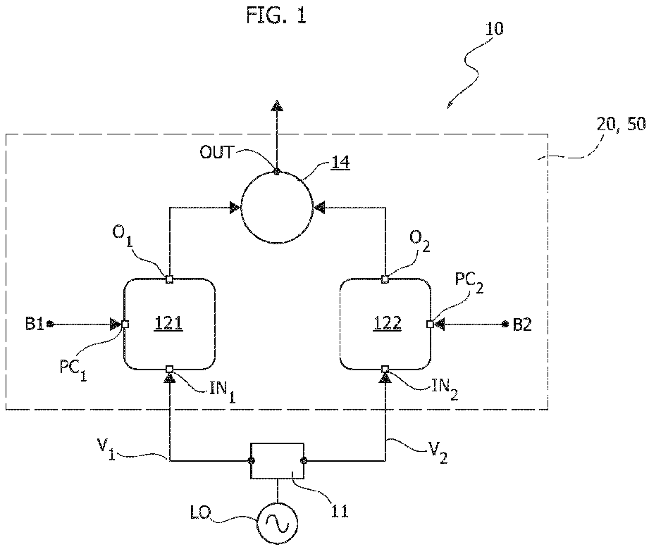
- Figure 1 is a diagram exemplary of a method as per the present disclosure,
- Figure 2 is a diagram exemplary of a circuit as per the present disclosure,
- Figures 3A, 3B and 3C are diagrams exemplary of frequency multiplication principles underlying one or more embodiments,
- Figures 4A, 4B, 4C and 4D are diagrams exemplary of phase shifting principles underlying one or more embodiments,
- Figure 5 is a diagram exemplary of a circuit as per the present disclosure,
- Figures 6 and 7 are diagrams exemplary of phase and amplitude of signals in one or more embodiments,
- Figure 8 is a diagram exemplary of a radar system equipped onboard a vehicle as per the present disclosure.
-
Corresponding numerals and symbols in the different figures generally refer to corresponding parts unless otherwise indicated.
-
The figures are drawn to clearly illustrate the relevant aspects of the embodiments and are not necessarily drawn to scale.
-
The edges of features drawn in the figures do not necessarily indicate the termination of the extent of the feature.
Detailed description
-
In the ensuing description, one or more specific details are illustrated, aimed at providing an in-depth understanding of examples of embodiments of this description. The embodiments may be obtained without one or more of the specific details, or with other methods, components, materials, etc. In other cases, known structures, materials, or operations are not illustrated or described in detail so that certain aspects of embodiments will not be obscured.
-
Reference to "an embodiment" or "one embodiment" in the framework of the present description is intended to indicate that a particular configuration, structure, or characteristic described in relation to the embodiment is comprised in at least one embodiment. Hence, phrases such as "in an embodiment" or "in one embodiment" that may be present in one or more points of the present description do not necessarily refer to one and the same embodiment.
-
Moreover, particular conformations, structures, or characteristics may be combined in any adequate way in one or more embodiments.
-
The references used herein are provided merely for convenience and hence do not define the extent of protection or the scope of the embodiments.
-
For the sake of simplicity, in the following detailed description a same reference symbol may be used to designate both a node/line in a circuit and a signal which may occur at that node or line.
-
As exemplified in Figure 1, a device 10 as per the present disclosure comprises:
- a radio-frequency signal generator RF configured to produce a first radio-frequency signal V1 having a first signal frequency f0,
- a quadrature generator 11 configured to provide a second radio-frequency signal V2 as an anteversion of the first radio-frequency signal V1; in other words, the second input signal V2 is in quadrature (that is, shifted by 90°) with the first input signal V1.
-
For instance, the first V
1 and second V
2 input signals can be expressed as:
-
As exemplified in Figure 1, the device 10 further comprises signal processing circuitry 20, 50 comprising:
- a first frequency converter circuit 121 comprising a first input node IN1 coupled to the RF signal generator and configured to receive the first input signal V1 therefrom, the first frequency converter circuit 121 further comprising a first control node PC1 configured to set a first control signal B1 (e.g., a first biasing current signal) and a first output node O1 configured to provide an output signal whose output signal frequency and phase are based on the first input signal V1 and the amplitude/intensity on the first control signal B1, as discussed in the following;
- a second frequency converter circuit 122 comprising a second input node IN2 coupled to the RF signal generator and configured to receive the second input signal V2 therefrom, the second frequency converter circuit 122 further comprising a second control node PC2 configured to set a second control signal B2 (e.g., a second biasing current signal) and a second output node O2 configured to provide an output signal whose output signal frequency and phase are based on the second input signal V2 and the amplitude/intensity on the second control signal B2, as discussed in the following;
- an output circuit block 14 (e.g., such as a resonant circuit LC tuned at a harmonic of the input signal frequency f0) coupled to the first 121 and second 122 frequency converter circuits to receive the first O1 and second O2 output signals therefrom (e.g., output current signals IO1, IO2) and configured to apply signal combination (e.g., superposition or subtraction) thereto, providing a frequency multiplied and phase shifted signal OUT to user circuits.
-
For instance, the first and the second control signals B1, B2 have different (e.g., signal intensity) values. For instance, the phase shift introduced by the device 10 on the output signal OUT varies (e.g., linearly) as a function of the ratio of the control signal B1, B2.
-
For instance, a first output signal O
1 produced by the first
frequency converter circuit 121 and a second output signal O
2 produced by the second
frequency converter circuit 122 can be expressed as:
where N is the frequency multiplication factor.
-
For instance, the further output signal OUT produced by the
output circuit block 14 as a result of combining (e.g., superimposing or subtracting) the output signals O
1, O
2 can be expressed as:
where
- B is the root mean square of the control signals B1 and B2, (i.e., ) and
- Θ is a phase-shift of the output signal.
-
For the sake of simplicity, one or more embodiments are discussed herein mainly with reference to switches comprising n-channel MOSFET switches, being otherwise understood that such a type of switch is purely exemplary and in no way limiting. One or more embodiments may employ p-channel MOSFET or BJT or virtually any other type of switch known per se.
-
A method as exemplified herein comprises:
- receiving IN1 a first input signal V1 oscillating at an input frequency f0;
- receiving PC1 a first set of control signals B1;
- receiving IN2 a second input signal V2 oscillating at the input frequency and in quadrature with the first input signal;
- receiving PC2 a second set of control signals B2;
- applying first signal processing 121; 521 to the first input signal and to control signals in the first set of control signals, providing a first output signal O1 as a result, the first output signal oscillating at an output frequency based on the input frequency and having an output signal amplitude based on the amplitude of at least one first control signal IB1 in the first set of control signals;
- applying second signal processing 122; 522 to the second input signal and to control signals in the second set of control signals, providing a second output signal O2 as a result, the second output signal oscillating at a second output frequency equal to the first output frequency and having an output signal amplitude based on the amplitude of at least one second control signal IB2 in the second set of control signals;
- based on the first output signal and the second output signal, providing 14 a further output signal OUT oscillating at an output signal frequency equal to the first output frequency and having a phase shift based on a ratio of signal amplitudes of at least one control signal in said first set of control signals and of at least one control signal in said second set of control signals.
-
As exemplified herein, control signals in the first B1 and second B2 set of control signals comprise biasing current signals IB1, IB2 and the further output signal OUT has a phase shift Θ based on a ratio of current intensities of at least one biasing current signal in said first set of control signals and of at least one biasing current signal in said second set of control signals.
-
A circuit 20; 50 as exemplified herein comprises:
- a first set of input nodes IN11, IN21; IN23, IN14 configured to receive a first input signal V1 oscillating at an input frequency f0;
- a first set of control nodes PC1; PC12, PC34 configured to receive a first set of control signals B1;
- a second set of input nodes IN12, IN22; IN32, IN41 configured to receive a second input signal V2 oscillating at the input frequency and in quadrature with the first input signal;
- a second set of control nodes PC2; PC21, PC34 configured to receive a second set of control signals B2;
- signal processing circuitry 121, 122; 521, 522 coupled to the first set of input nodes, to the first set of control nodes, to the second set of input nodes and to the second set of control nodes and having a further output circuit block 14,
- wherein the signal processing circuitry is configured to provide a further output signal OUT at said further output node according to the method as exemplified herein, the further output signal oscillating at an output signal frequency equal to the first output frequency and having a phase shift based on a ratio of signal amplitudes of at least one first control signal in said first set of control signals and of at least one second control signal in said second set of control signals.
-
The circuit 20; 50 as exemplified herein can be included in a device 10 further comprising a frequency synthesizer LO, 11 coupled to the circuit and configured to provide thereto the input signals oscillating at the input frequency.
-
For instance, the frequency synthesizer LO, 11 is configured to provide said input signals oscillating at the input frequency such that the output frequency of the further signal lies in the millimeter wavelength range.
-
A system as exemplified herein comprises:
- a device 10 as per the present disclosure;
- a power amplifier 180 coupled to the circuit and configured to receive the further output signal OUT therefrom, the power amplifier configured to amplify the further output signal and to provide an amplified output signal TX as a result, and
- a transmitter antenna 20 coupled to the power amplifier and configured to transmit the amplified output signal. For instance, the system includes a vehicular radar system.
-
As exemplified herein, a vehicle V can be equipped with a vehicular radar system comprising:
- a receiver antenna 22 configured to receive an echo signal based on the transmitted amplified output signal,
- a mixer stage 28 coupled to the circuit as per the present disclosure, the mixer stage configured to apply frequency mixing to the further output signal and to the echo signal, producing a mixed signal as a result.
-
In a first exemplary scenario illustrated in Figure 2, signal processing circuitry 20 as per the present disclosure comprises:
- a first (e.g., fully) differential pair of switches M11, M21 comprising a first (e.g., n-channel MOSFET) switch M11 and a second (e.g., n-channel MOSFET) switch M21 configured to have the first input signal V1 applied among switch control nodes IN11, IN21 and coupled to a first biasing (e.g., current) signal generator 1210 referred to ground GND to receive a first biasing (e.g., current) signal IB1 therefrom, the first differential pair of switches M11, M21 configured to provide a differential output signal among differential output nodes O1, O2; for instance, the first switch Mu has a first control node IN11, a first output node O1 and a first source node PC1 coupled to a second source node of a second switch M21 which has a respective second control node IN21 and second output node O2;
- a second (e.g., fully) differential pair of switches M12, M22 comprising a third (e.g., n-channel MOSFET) switch M12 and a fourth (e.g., n-channel MOSFET) switch M22 configured to have the second input signal V2 applied among switch control nodes IN12, IN22 and coupled to a second biasing (e.g., current) signal generator 1220 referred to ground GND to receive a second biasing (e.g., current) signal IB2 therefrom, the second differential pair of switches M12, M22 configured to provide a differential output signal among differential output nodes O1, O2; for instance, the third switch M12 has a third control node IN12, a third output node and a third source node PC2 coupled to a fourth source node of the fourth switch M22 which has a respective fourth control node IN22 and fourth output node.
-
As exemplified in Figure 2, the first output node O1 of the first differential pair Mu, M21 is coupled to the third output node of the second differential pair M12, M22 while the second output node O2 of the first differential pair M11, M21 is coupled to the fourth output node of the second differential pair M12, M22.
-
As exemplified in Figure 2, the first 121 and second 122 frequency converter circuits are coupled to a set of load circuits Z1, Z2 comprising:
- a first load circuit Z1 comprising a first RLC network, e.g., comprising a first resistive element R1 in parallel to a first capacitive element C1 and to a first inductive element L1;
- a second load circuit Z2 comprising a second RLC network, e.g., comprising a second resistive element R2 in parallel to a second capacitive element C2 and to a second inductive element L2.
-
As exemplified in Figure 2, the load circuits Z1, Z2 are coupled to a biasing node VDD configured to provide a supply voltage VDD and have a circuit output nodes O1, O2 configured to provide an output signal OUT as a combination (e.g., superposition) of the differential output signals IO1, IO2 provided by the frequency converter circuits 121, 122, the output signal OUT having a frequency based on (e.g., multiple of) the input frequency f0 of the input signals V1, V2.
-
In order to do so, the passive electrical components L
1, C
1 and L
2, C
2 in the first Z
1 and second Z
2 load circuits are tuned at a desired N-th harmonic of the input signal frequency f
0, based on the relation between resonant frequency and capacitance/inductance which may be expressed as
.
-
As exemplified in Figure 2, the intensities IO1, IO2 of electrical currents generated by the current generators 1210, 1220 may be varied by the user depending on the application. For instance, setting different intensity values for the electrical currents IO1, IO2 introduces a phase difference between signals output from the first frequency converter circuit 121 and the second frequency converter circuit 122, as discussed in the following.
-
For instance, the phase shift is a result of the combination (e.g., superposition or difference) at the output circuit block 14 (e.g., implemented via the resonant loads Z1, Z2) of the output current signals produced by each differential circuit 121, 122.
-
A method of driving the circuit 20 as per the present disclosure comprises:
- driving the first differential pair M11, M21 by applying the first input signal V1 at the control nodes IN11, IN21 of the first differential pair M11, M21, alternatively making conductive a current flow path through the first switch M11 while making non-conductive a current flow path through the second switch M21;
- driving the second differential pair M12, M22 by applying the second input signal V2 (which is in quadrature with the first input signal V1) at the control nodes IN12, IN22 of the second differential pair M12, M22, alternatively making conductive a current flow path through the fourth switch M22 while making non-conductive a current flow path through the third switch M12.
-
As a result, the first biasing current signal IB1 generated by the first current generator 1210 and the second biasing current signal IB2 generated by the second current generator 1220 are each multiplied by a square wave of unitary amplitude.
-
Therefore, a first output current signal I
O1 comprises a square wave output comprising odd harmonics of the first input signal V
1.
where
I
B1 is the biasing current provided by the first
current generator 1210.
-
Similarly, a second output current signal I
O2 comprises a square wave output comprising odd harmonics of the second input signal V
2 and can be expressed as:
-
As exemplified in Figure 2, the LC resonant loads Z 1, Z2 filter the undesired (odd) harmonics.
-
As exemplified in
Figures 1 and
2, a
frequency multiplier circuit 10, 50 having an odd multiplication factor of (2N+1) can be obtained by tuning the LC resonant load Z
1, Z
2 at the (2N+1)-th off harmonics of the input signal V
1, which may be expressed as:
-
Figures 3A-3C are diagrams exemplary of a spectral content of the frequency multiplied signal at various multiples of the input signal frequency f0.
-
For instance, a
frequency multiplier circuit 10, 20 having multiplication factor of three can be obtained by tuning the LC resonator at the 3rd harmonics of the input signal Vi. In such an exemplary case, the i-th differential output signal I
Oi can be expressed as:
-
For instance, if the input signal Vi has an input signal frequency f0 about 26 GHz, a multiplier circuit 20 with multiplication factor of 3 can provide an output signal OUT having an output signal frequency four about 78 GHz.
-
Figure 3A is a diagram exemplary of a spectral content of the frequency multiplied signal at frequency multiple three times the input signal frequency f0.
-
In a further exemplary scenario, a frequency multiplier by five is obtained by tuning the LC resonator at the 5th harmonic of the input signal Vi. In such an exemplary case, the i-th differential output signal I
O1 can be expressed as:
-
Figure 3B is a diagram exemplary of a spectral content of the frequency multiplied signal at frequency multiple five times the input signal frequency f0.
-
As exemplified in Figures 4A-4B, a differential output current of the two circuit cells which receive input signals V1, V2 in quadrature therebetween comprises of sum of two orthogonal vectors IO1, IO2 whose intensities can be modulated by changing the biasing currents IB1, IB2 provided by the respective biasing current generators 1210, 1220.
-
For instance, the current intensities of output signals I
O1, I
O2 may be expressed as:
-
A current intensity of the output current signal I
O can be expressed as a sum of the output current signals I
O1, I
O2, such as:
-
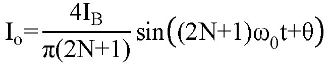
As exemplified in Figures 1 and 2, an output voltage signal OUT is equal to a differential voltage at nodes O1 and O2. As exemplified in Figure 2, an output voltage can be expresses as OUT = Io x R where Io is the output current and R may be expressed as R = R1+R2, in case the resonant networks L1C1 and L2C2 resonate at a frequency f which is an odd multiple of the input frequency f0, namely f =(2N+1)*fo.
-
As exemplified herein, a method of operating the circuit 10, 20 comprises performing phase shifting based on differential output signals IO1, IO2 output by respective circuit units 121, 122. For instance, a sum current IO (which may be expressed as IO=IO1+IO2) is based on the sum of two vectors IO1, IO2 in quadrature therebetween and having different amplitudes/intensity, thereby varying the phase-shift of the sum signal OUT, IO.
-
For instance, performing phase shifting comprises setting the ratio of intensities of biasing currents IB1, IB2 produced by biasing generators 1211, 1221 to have a ratio equal to the tangent of a phase shift angle Θ, providing a linear phase shift of the sum signal OUT, IO based on differential output signals IO1, IO2 as a result.
-
As exemplified in
Figure 4A, if the phase shift Θ to introduce falls in a
range 0° to 90°, a ratio of biasing current intensities can be expressed as:
-
In other words, the phase shift Θ of the output signal OUT resulting from a differential voltage signal based on the first output signal O
1 and the second output signal O
2 is based on a ratio of the signal amplitudes of control signals (e.g., equal to current intensities in case of biasing current signals), which can be expressed as:
where arctan is an inverse function of the trigonometric tangent function.
-
In such an exemplary scenario, a first intensity I
B1 of the biasing current generated by the first biasing current generator 1211 can be expressed as:
-
Still in the exemplary scenario considered, a second intensity I
B2 of the biasing current generated by the second biasing current generator 1211 can be expressed as:
-
As a result, the output current signal has an output current intensity I
O which can be expressed as:
-
Exploiting trigonometric equivalence, the output current intensity I
O of the output signal OUT can be expressed as:
-
A circuit and method as exemplified facilitate an increased robustness over PVT variations thanks to the use of the biasing current to vary the phase shift.
-
An arrangement as exemplified in Figure 2 facilitates varying the phase shift Θ of the output signal OUT within at least one quadrant of the turn angle.
-
It may be possible to vary the phase shift also in the entire turn angle, that is in a range of linear phase shift angle values from 0° to 360°, for instance by changing sign and amplitude of biasing currents IB1, IB2.
-
Figures 4B to 4D are diagrams exemplary of a way of representing the total current IO as a vector whose orientation in a complex plane is a function of the first and second output signals IO1, IO2, whose relative orientation varies as a function of the biasing current values IB1, IB2, as discussed in the foregoing.
-
In an alternative scenario exemplified in Figure 5, an alternative circuit 50 for use in the device 10 comprises, in place of the first frequency converter circuit 121 and the second frequency converter circuit 122 in the circuit 20 exemplified in Figure 2:
- a first alternative (e.g., double-balanced) frequency converter circuit 521 comprising a Gilbert-cell like arrangement comprising two (pairs of) differential pairs of (e.g., n-channel MOSFET) switches Q11, Q12, Q13, Q14, each replicating the arrangement of the first differential pair M11, M21 exemplified in Figure 2 save for the way in which the control nodes of the switches are driven, as discussed in the following; and
- a second alternative (e.g., double-balanced) frequency converter circuit 522 comprising a further Gilbert-cell like arrangement comprising two further (pairs of) differential pairs of (e.g., n-channel MOSFET) switches Q21, Q22, Q23, Q24, each replicating the arrangement of the second differential pair M12, M22 exemplified in Figure 2 save for the way in which the control nodes of the switches are driven, as discussed in the following.
-
As exemplified in Figure 5, the first alternative frequency converter circuit 521 comprises:
- a first differential pair of switches Q11, Q12 comprising a first switch Q11 having a control node IN14 coupled to the respective control node of a fourth switch Q14 and a first biasing node PC12 coupled to the respective biasing node of a second switch Q12 having a control node IN23 coupled to a respective control node of a third switch Q13;
- a second differential pair of switches Q13, Q14 comprising the third switch Q13 having the control node IN23 coupled to the control node of the second switch Q12 in the first differential pair Q11, Q12 and a second biasing node PC34 coupled to the biasing node of the fourth switch Q14 having the control node IN14 coupled to the respective control node of the first switch Q11 in the first differential pair Q11, Q12;
- a first biasing current generator 5211 coupled to the first biasing node PC12 of the first differential pair Q11, Q12 to provide a first biasing current IB11 thereto, and
- a second biasing current generator 5212 coupled to the second biasing node PC34 of the second differential pair Q13, Q14 to provide a second biasing current IB22 thereto.
-
As exemplified in Figure 5, the second alternative frequency converter circuit 522 comprises:
- a third differential pair of switches Q21, Q22 comprising a fifth switch Q21 having a control node IN41 coupled to the respective control node of an eight switch Q24 and a third biasing node PC21 coupled to the respective biasing node of a sixth switch Q22 having a control node IN32 coupled to a respective control node IN32 of a seventh switch Q23;
- a fourth differential pair of switches Q23, Q24 comprising the seventh switch Q23 having the control node IN32 coupled to respective control node IN32 of the sixth switch Q22 in the third differential pair Q21, Q22 and a fourth biasing node PC34 coupled to the biasing node of the eight switch Q24 having the control node IN41 coupled to the respective control node IN41 of the fifth switch Q21 in the third differential pair Q21, Q22;
- a third biasing current generator 5221 coupled to the third biasing node PC21 of the third differential pair Q21, Q22 to provide a third biasing current IB21 thereto, and
- a fourth biasing current generator 5222 coupled to the fourth biasing node PC34 of the fourth differential pair Q23, Q24 to provide a fourth biasing current IB22 thereto.
-
As exemplified in Figure 5, operating the circuit 50 comprises:
- applying a first input signal V1 among the control nodes IN23, IN14 of the first alternative frequency converter circuit 521,
- applying a second input signal V2 (is in quadrature with the first input signal V1) among the control nodes IN32, IN41 of the second alternative frequency converter circuit 522,
- setting the current intensity values IB11, IB12, IB21, IB22 of biasing currents generated via the first, second, third and fourth biasing current generators 5211, 5212, 5221, 5222 to produce a phase shift of the output signal.
-
The alternative circuit 50 exemplified in Figure 5 with respect to the circuit 20 exemplified in Figure 2 facilitates further increasing robustness versus PVT variations thanks to the possibility to have some current generators deactivated in varying the phase shift in a range of linear phase shift angle values 0° to 360°.
-
For instance, the current intensities I
B11, I
B12, I
B21, I
B22 for different ranges of phase shift values Θ may be expressed as:
-
In other words, based on intensity values of at least one further control signal IB11, IB12, IB21, IB22 and at least one control signal IB1, IB2 being based on the biasing phase shift value Θ it is possible to alternately apply the input voltages V1, V2, with alternating phases to the differential input nodes IN1, IN2 of the circuit 20, 50. Without being bound to a specific theoretical model, this can be the result of turning alternatively ON and OFF transistors in the differential pairs of transistors as a result of setting at least two control signals at zero intensity/amplitude.
-
In variant embodiments, it may be possible to vary the four current intensity values IB11, IB12, IB21, IB22 as a function of the two parameters β1, β2 with respect to their sum IB.
-
For instance, in such an alternative scenario the biasing current intensity values I
B11, I
B12, I
B21, I
B22 can be expressed as:
where the considerations expressed in the foregoing with reference to
Figures 4A-4D can be applied likewise to determine the values of the parameters β
1, β
2.
-
In the considered variant embodiments, to extend the range of applicable phase shift Θ to at least two quadrants of the turn angle, the values of current intensity parameter β
1, β
2 may be expressed as:
where α is a user settable parameter whose value is greater than unity or one.
-
The circuits 20, 50 as exemplified herein can be integrated circuits, for instance integrated in a 28nm FD-SOI CMOS technology (per se known).
-
Figure 6 shows a plot of the phase of the output signal OUT provided by the circuits 10, 20, 50 as a function of the phase shift Θ, which is indicative of the linear type relationship among the two parameters.
-
Figure 7 shows a plot of amplitude of the output signal OUT provided by the device 10 comprising the circuit 20 or 50 as a function of the phase shift Θ, which is indicative of the fact that the amplitude of the signal remains substantially constant during phase-shift variations.
-
In a method as exemplified herein, providing 14 the further output signal OUT comprises:
- providing at least one resonant network stage R1, L1, C1; R2, C2, L2 and tuning the at least one (resonant) network stage to resonate at an odd integer multiple of the input frequency f0 of the first, resp. second, input signal V1, V2, and
- applying resonant filtering Z1, Z2 to a signal based on the first O1 and the second O2 amplified difference signals, producing the further output (e.g., voltage) signal OUT as a result.
-
In a first exemplary scenario exemplified in Figure 2, applying said first signal processing 121; 521 and said second signal processing 122; 522 comprises:
- providing a first signal amplification processing stage M11, M21; Q11, Q12, Q13, Q14 and a second signal amplification processing stage M12, M22; Q21, Q22, Q23, Q24, the first, resp. second, signal amplification processing stage comprising at least one differential pair of transistors having current flow paths therethrough configured to be made selectively conductive and non-conductive based on the first, resp. second, input signal and having a common biasing node therebetween;
- coupling, to the first signal amplification processing stage, a first set of current generators 1210; 5211, 5212 configured to provide the first set of control signals;
- coupling, to the second signal amplification processing stage, a first set of current generators 1220; 5221, 5222 configured to provide the second set of control signals.
-
As exemplified herein, the method comprises:
- coupling at least one resonant network stage to the first and to the second signal amplification processing stages;
- tuning the at least one network stage to resonate at an odd integer multiple of the input frequency of the first, resp. second, input signal, and
- applying resonant filtering to a difference among the first and the second amplified difference signals, producing the further output signal as a result,
- wherein the further output signal comprises a voltage signal.
-
For instance, the method comprises varying said phase shift Θ within at least one quarter of the turn angle.
-
As exemplified herein:
- the first set of control signals B1 comprises a first plurality of biasing current signals IB11, IB12;
- the second set of control signals B2 comprises a second plurality of biasing current signal IB21, IB22, and
- at least one biasing current signal in first plurality of biasing current signals and at least one biasing current signal in the second plurality of biasing current signal is equal to zero.
-
As exemplified herein:
- the first set of control signals B1 comprises a first biasing current signal IB11 and a second biasing current signal IB12;
- the second set of control signals B2 comprises a third biasing current signal IB21 and a fourth biasing current signal IB22.
-
For instance:
- the first biasing current signal has a first biasing intensity equal to a common biasing IB intensity plus a first biasing coefficient β1;
- the second biasing current signal has a second biasing intensity equal to the common biasing intensity IB minus the first biasing coefficient β1;
- the third biasing current signal has a third biasing intensity equal to the common biasing intensity IB plus a second biasing coefficient β2;
- the fourth biasing current signal has a fourth biasing intensity equal to the common biasing intensity IB minus the second biasing coefficient β2;
- said phase shift Θ is equal to an arc-tangent of the ratio of the first biasing coefficient β1 and the second biasing coefficient β2.
-
As exemplified herein, said first biasing coefficient β1 and said second biasing coefficient β2 are based on a ratio of the common current intensity IB and an integer value α greater than one.
-
As exemplified in Figure 8, a vehicle V can be equipped with a radar system 80 comprising a device 10 as per the present disclosure and antennas 21, 22 in order to detect an object O, for instance an obstacle along a traveling path of the vehicle V.
-
Distance R (and speed) of the object O can be detected by measuring a time delay d between a transmitted signal (whose wave-front is shown in solid lines) having a carrier signal frequency f0 and the received echo signal (whose wave-front is shown in dashed lines) having a spectral content f0±fd spread over the carrier radio-frequency signal at frequency f0.
-
As exemplified in Figure 8, a radar transceiver system 80 comprises:
- a transmitter chain 18 configured to provide a RF signal to a transmitting antenna (e.g., array) 21,
- a receiver chain 24 configured to detect the echo signal reflected from the obstacle O via a receiver antenna (e.g., array) 22,
- a processing system 30 configured to drive the transmission of signals from the transmitter chain 18 and to process signals detected by the receiver chain 24.
-
As exemplified in Figure 8, the transmitter chain 18 comprises:
- a frequency synthesizer LO, such as a phase-locked loop (briefly, PLL) configured to generate the first input signal V1 configured to provide a subharmonic of the operating frequency, e.g., to counter frequency pulling from the power amplifier;
- a quadrature generator 11 coupled to the frequency synthesizer LO to provide the second input signal V2 as an antiphase or quadrature version of the first input signal V1;
- a circuit (implemented in the single 20 or double balanced 50 topologies, for instance) coupled to the frequency synthesizer LO and to the phase-shifter to receive the first V1 and second V2 input signals therefrom, the circuit 20, 50 configured to perform frequency multiplication and to apply a linear phase shift Θ to the input signals V1, V2, providing as a result an output signal OUT which comprises an odd harmonic of the RF signal and has a phase shift Θ which is a function of user-settable parameters B1, B2;
- a (transmitter) amplifier 180, e.g., a variable-gain amplifier (briefly, VGA) or a power amplifier (briefly, PA), coupled to the circuit 20, 50 to receive the (odd) harmonic OUT of the RF signal V1 therefrom, the amplifier 180 configured to amplify the harmonic of the RF signal produced via the circuit 20, 50 and to operate/drive the transmission (briefly, TX) antenna (array) 21 therewith.
-
As exemplified in Figure 8, the corresponding incoming (echo) signal received at a receiving (briefly, RX) antenna 22 is fed to the receiver chain 24, comprising:
- a low noise amplifier (briefly, LNA) 26, coupled to the receiver antenna (e.g., array) 22 to receive the echo signal therefrom, and
- a frequency converter stage 28 coupled to the LNA 26 to receive the detected echo signal therefrom and coupled to the PLL to receive the local oscillator signal LO therefrom, the frequency converter stage 28 configured to produce a down-converted frequency signal IF based on the echo signal and the LO signal, in a manner per se known.
-
In one or more embodiments, the radar system 80 may be a system-on-chip integrated in a semiconductor device. For instance, the proposed system can be integrated in a 28-nm FD-SOI CMOS technology device equipped on-board a transmitter stage of a mm-wave 77GHz CMOS radar system.
-
It will be otherwise understood that the various individual implementing options exemplified throughout the figures accompanying this description are not necessarily intended to be adopted in the same combinations exemplified in the figures. One or more embodiments may thus adopt these (otherwise non-mandatory) options individually and/or in different combinations with respect to the combination exemplified in the accompanying figures.
-
Without prejudice to the underlying principles, the details and embodiments may vary, even significantly, with respect to what has been described by way of example only, without departing from the extent of protection. The extent of protection is defined by the annexed claims.