EP4498767A1 - Stiffener member with one or more vias - Google Patents
Stiffener member with one or more vias Download PDFInfo
- Publication number
- EP4498767A1 EP4498767A1 EP24190960.5A EP24190960A EP4498767A1 EP 4498767 A1 EP4498767 A1 EP 4498767A1 EP 24190960 A EP24190960 A EP 24190960A EP 4498767 A1 EP4498767 A1 EP 4498767A1
- Authority
- EP
- European Patent Office
- Prior art keywords
- substrate
- connector
- area
- circuit board
- adjacent
- Prior art date
- Legal status (The legal status is an assumption and is not a legal conclusion. Google has not performed a legal analysis and makes no representation as to the accuracy of the status listed.)
- Pending
Links
Images









Classifications
-
- H—ELECTRICITY
- H10—SEMICONDUCTOR DEVICES; ELECTRIC SOLID-STATE DEVICES NOT OTHERWISE PROVIDED FOR
- H10W—GENERIC PACKAGES, INTERCONNECTIONS, CONNECTORS OR OTHER CONSTRUCTIONAL DETAILS OF DEVICES COVERED BY CLASS H10
- H10W74/00—Encapsulations, e.g. protective coatings
- H10W74/10—Encapsulations, e.g. protective coatings characterised by their shape or disposition
- H10W74/111—Encapsulations, e.g. protective coatings characterised by their shape or disposition the semiconductor body being completely enclosed
- H10W74/114—Encapsulations, e.g. protective coatings characterised by their shape or disposition the semiconductor body being completely enclosed by a substrate and the encapsulations
-
- H—ELECTRICITY
- H05—ELECTRIC TECHNIQUES NOT OTHERWISE PROVIDED FOR
- H05K—PRINTED CIRCUITS; CASINGS OR CONSTRUCTIONAL DETAILS OF ELECTRIC APPARATUS; MANUFACTURE OF ASSEMBLAGES OF ELECTRICAL COMPONENTS
- H05K1/00—Printed circuits
- H05K1/02—Details
- H05K1/11—Printed elements for providing electric connections to or between printed circuits
- H05K1/115—Via connections; Lands around holes or via connections
-
- H—ELECTRICITY
- H10—SEMICONDUCTOR DEVICES; ELECTRIC SOLID-STATE DEVICES NOT OTHERWISE PROVIDED FOR
- H10W—GENERIC PACKAGES, INTERCONNECTIONS, CONNECTORS OR OTHER CONSTRUCTIONAL DETAILS OF DEVICES COVERED BY CLASS H10
- H10W70/00—Package substrates; Interposers; Redistribution layers [RDL]
- H10W70/60—Insulating or insulated package substrates; Interposers; Redistribution layers
- H10W70/67—Insulating or insulated package substrates; Interposers; Redistribution layers characterised by their insulating layers or insulating parts
- H10W70/68—Shapes or dispositions thereof
- H10W70/685—Shapes or dispositions thereof comprising multiple insulating layers
-
- H—ELECTRICITY
- H05—ELECTRIC TECHNIQUES NOT OTHERWISE PROVIDED FOR
- H05K—PRINTED CIRCUITS; CASINGS OR CONSTRUCTIONAL DETAILS OF ELECTRIC APPARATUS; MANUFACTURE OF ASSEMBLAGES OF ELECTRICAL COMPONENTS
- H05K1/00—Printed circuits
- H05K1/02—Details
- H05K1/0271—Arrangements for reducing stress or warp in rigid printed circuit boards, e.g. caused by loads, vibrations or differences in thermal expansion
-
- H—ELECTRICITY
- H05—ELECTRIC TECHNIQUES NOT OTHERWISE PROVIDED FOR
- H05K—PRINTED CIRCUITS; CASINGS OR CONSTRUCTIONAL DETAILS OF ELECTRIC APPARATUS; MANUFACTURE OF ASSEMBLAGES OF ELECTRICAL COMPONENTS
- H05K1/00—Printed circuits
- H05K1/02—Details
- H05K1/14—Structural association of two or more printed circuits
- H05K1/141—One or more single auxiliary printed circuits mounted on a main printed circuit, e.g. modules, adapters
-
- H—ELECTRICITY
- H10—SEMICONDUCTOR DEVICES; ELECTRIC SOLID-STATE DEVICES NOT OTHERWISE PROVIDED FOR
- H10W—GENERIC PACKAGES, INTERCONNECTIONS, CONNECTORS OR OTHER CONSTRUCTIONAL DETAILS OF DEVICES COVERED BY CLASS H10
- H10W20/00—Interconnections in chips, wafers or substrates
- H10W20/20—Interconnections within wafers or substrates, e.g. through-silicon vias [TSV]
-
- H—ELECTRICITY
- H10—SEMICONDUCTOR DEVICES; ELECTRIC SOLID-STATE DEVICES NOT OTHERWISE PROVIDED FOR
- H10W—GENERIC PACKAGES, INTERCONNECTIONS, CONNECTORS OR OTHER CONSTRUCTIONAL DETAILS OF DEVICES COVERED BY CLASS H10
- H10W20/00—Interconnections in chips, wafers or substrates
- H10W20/40—Interconnections external to wafers or substrates, e.g. back-end-of-line [BEOL] metallisations or vias connecting to gate electrodes
-
- H—ELECTRICITY
- H10—SEMICONDUCTOR DEVICES; ELECTRIC SOLID-STATE DEVICES NOT OTHERWISE PROVIDED FOR
- H10W—GENERIC PACKAGES, INTERCONNECTIONS, CONNECTORS OR OTHER CONSTRUCTIONAL DETAILS OF DEVICES COVERED BY CLASS H10
- H10W70/00—Package substrates; Interposers; Redistribution layers [RDL]
- H10W70/01—Manufacture or treatment
- H10W70/05—Manufacture or treatment of insulating or insulated package substrates, or of interposers, or of redistribution layers
-
- H—ELECTRICITY
- H10—SEMICONDUCTOR DEVICES; ELECTRIC SOLID-STATE DEVICES NOT OTHERWISE PROVIDED FOR
- H10W—GENERIC PACKAGES, INTERCONNECTIONS, CONNECTORS OR OTHER CONSTRUCTIONAL DETAILS OF DEVICES COVERED BY CLASS H10
- H10W70/00—Package substrates; Interposers; Redistribution layers [RDL]
- H10W70/60—Insulating or insulated package substrates; Interposers; Redistribution layers
- H10W70/62—Insulating or insulated package substrates; Interposers; Redistribution layers characterised by their interconnections
- H10W70/63—Vias, e.g. via plugs
- H10W70/635—Through-vias
-
- H—ELECTRICITY
- H10—SEMICONDUCTOR DEVICES; ELECTRIC SOLID-STATE DEVICES NOT OTHERWISE PROVIDED FOR
- H10W—GENERIC PACKAGES, INTERCONNECTIONS, CONNECTORS OR OTHER CONSTRUCTIONAL DETAILS OF DEVICES COVERED BY CLASS H10
- H10W70/00—Package substrates; Interposers; Redistribution layers [RDL]
- H10W70/60—Insulating or insulated package substrates; Interposers; Redistribution layers
- H10W70/67—Insulating or insulated package substrates; Interposers; Redistribution layers characterised by their insulating layers or insulating parts
- H10W70/69—Insulating materials thereof
-
- H—ELECTRICITY
- H05—ELECTRIC TECHNIQUES NOT OTHERWISE PROVIDED FOR
- H05K—PRINTED CIRCUITS; CASINGS OR CONSTRUCTIONAL DETAILS OF ELECTRIC APPARATUS; MANUFACTURE OF ASSEMBLAGES OF ELECTRICAL COMPONENTS
- H05K1/00—Printed circuits
- H05K1/02—Details
- H05K1/14—Structural association of two or more printed circuits
- H05K1/144—Stacked arrangements of planar printed circuit boards
-
- H—ELECTRICITY
- H05—ELECTRIC TECHNIQUES NOT OTHERWISE PROVIDED FOR
- H05K—PRINTED CIRCUITS; CASINGS OR CONSTRUCTIONAL DETAILS OF ELECTRIC APPARATUS; MANUFACTURE OF ASSEMBLAGES OF ELECTRICAL COMPONENTS
- H05K2201/00—Indexing scheme relating to printed circuits covered by H05K1/00
- H05K2201/06—Thermal details
- H05K2201/068—Thermal details wherein the coefficient of thermal expansion is important
-
- H—ELECTRICITY
- H05—ELECTRIC TECHNIQUES NOT OTHERWISE PROVIDED FOR
- H05K—PRINTED CIRCUITS; CASINGS OR CONSTRUCTIONAL DETAILS OF ELECTRIC APPARATUS; MANUFACTURE OF ASSEMBLAGES OF ELECTRICAL COMPONENTS
- H05K2201/00—Indexing scheme relating to printed circuits covered by H05K1/00
- H05K2201/09—Shape and layout
- H05K2201/09209—Shape and layout details of conductors
- H05K2201/095—Conductive through-holes or vias
- H05K2201/09563—Metal filled via
-
- H—ELECTRICITY
- H05—ELECTRIC TECHNIQUES NOT OTHERWISE PROVIDED FOR
- H05K—PRINTED CIRCUITS; CASINGS OR CONSTRUCTIONAL DETAILS OF ELECTRIC APPARATUS; MANUFACTURE OF ASSEMBLAGES OF ELECTRICAL COMPONENTS
- H05K2201/00—Indexing scheme relating to printed circuits covered by H05K1/00
- H05K2201/09—Shape and layout
- H05K2201/09209—Shape and layout details of conductors
- H05K2201/095—Conductive through-holes or vias
- H05K2201/09572—Solder filled plated through-hole in the final product
-
- H—ELECTRICITY
- H05—ELECTRIC TECHNIQUES NOT OTHERWISE PROVIDED FOR
- H05K—PRINTED CIRCUITS; CASINGS OR CONSTRUCTIONAL DETAILS OF ELECTRIC APPARATUS; MANUFACTURE OF ASSEMBLAGES OF ELECTRICAL COMPONENTS
- H05K2201/00—Indexing scheme relating to printed circuits covered by H05K1/00
- H05K2201/10—Details of components or other objects attached to or integrated in a printed circuit board
- H05K2201/10227—Other objects, e.g. metallic pieces
- H05K2201/10378—Interposers
-
- H—ELECTRICITY
- H05—ELECTRIC TECHNIQUES NOT OTHERWISE PROVIDED FOR
- H05K—PRINTED CIRCUITS; CASINGS OR CONSTRUCTIONAL DETAILS OF ELECTRIC APPARATUS; MANUFACTURE OF ASSEMBLAGES OF ELECTRICAL COMPONENTS
- H05K2201/00—Indexing scheme relating to printed circuits covered by H05K1/00
- H05K2201/20—Details of printed circuits not provided for in H05K2201/01 - H05K2201/10
- H05K2201/2009—Reinforced areas, e.g. for a specific part of a flexible printed circuit
-
- H—ELECTRICITY
- H05—ELECTRIC TECHNIQUES NOT OTHERWISE PROVIDED FOR
- H05K—PRINTED CIRCUITS; CASINGS OR CONSTRUCTIONAL DETAILS OF ELECTRIC APPARATUS; MANUFACTURE OF ASSEMBLAGES OF ELECTRICAL COMPONENTS
- H05K3/00—Apparatus or processes for manufacturing printed circuits
- H05K3/40—Forming printed elements for providing electric connections to or between printed circuits
- H05K3/4038—Through-connections; Vertical interconnect access [VIA] connections
-
- H—ELECTRICITY
- H10—SEMICONDUCTOR DEVICES; ELECTRIC SOLID-STATE DEVICES NOT OTHERWISE PROVIDED FOR
- H10W—GENERIC PACKAGES, INTERCONNECTIONS, CONNECTORS OR OTHER CONSTRUCTIONAL DETAILS OF DEVICES COVERED BY CLASS H10
- H10W44/00—Electrical arrangements for controlling or matching impedance
- H10W44/20—Electrical arrangements for controlling or matching impedance at high-frequency [HF] or radio frequency [RF]
- H10W44/203—Electrical connections
Definitions
- the present disclosure relates, in general, to methods, systems, and apparatuses for implementing a semiconductor package or a chip package, and more particularly to methods, systems, and apparatuses for implementing a semiconductor package or a chip package including a stiffener member with one or more vias.
- Various embodiments provide tools and techniques for implementing semiconductor packages or chip packages including a stiffener member with one or more vias.
- an apparatus including a substrate.
- a connector is coupled to the substrate.
- a member is disposed between the substrate and the connector. The member restrains at least one of the substrate or the connector. Additionally, a via extends through a body of the member. The via couples to the connector and to the substrate.
- an area of a first surface of the member adjacent to a first surface of the substrate is characterized by about a same area size as an area of the first surface of the substrate.
- the member is configured to uniformly restrain the substrate across the area of the first surface of the substrate.
- an area of a first surface of the member adjacent to a first surface of the substrate is smaller than a second surface of the member adjacent to a first surface of the connector.
- the connector comprises a printed circuit board.
- An area of a second surface of the member adjacent to a first surface of the printed circuit board is characterized by about a same area size as an area of the first surface of the printed circuit board.
- the connector comprises at least one of an optical connector, a high-speed data connector, a high-power connector, or a backplane connector, or the like.
- An area of a second surface of the member adjacent to a first surface of at least one of the optical connector, the high speed data connector, the high power connector, or the backplane connector is characterized by about a same area size or larger area size as an area of the first surface of at least one of the optical connector, the high speed data connector, the high power connector, or the backplane connector.
- the member has about a same coefficient of thermal expansion as the substrate.
- the member comprises at least one of copper, aluminum, ceramic, steel, stainless steel, Teflon, silicon, or polymer, and the via comprises at least one of copper, aluminum, gold, silver, tin, nickel, or lead.
- the member comprises at least two adjacent vias. A ratio between a distance between the at least two adjacent vias and a width of each via of the at least two adjacent vias is at least 2:1. A ratio between a length of the member and a thickness of the member is equal or greater than 10:1.
- a semiconductor device comprises a substrate comprising an interconnect, a connector configured to couple to the interconnect of the substrate, and a member between the substrate and the connector.
- the member is configured to restrain at least one of the substrate or the connector.
- a via extends through the member and couples the interconnect of the substrate to the connector.
- a first surface of the member adjacent to a first surface of the substrate uniformly restrains the substrate across the first surface of the substrate. In some instances, an area of a first surface of the member adjacent to a first surface of the substrate is larger than an area of the first surface of the substrate.
- the connector comprises a printed circuit board.
- a second surface of the member adjacent to a first surface of the printed circuit board uniformly restrains the printed circuit board across the first surface of the printed circuit board.
- the connector comprises at least one of an optical connector, a high-speed data connector, a high-power connector, or a backplane connector, or the like.
- the via is located in a first layer of the member, and the member further comprises a second redistribution layer electrically coupled to the via.
- a method of manufacturing a semiconductor with a member includes providing a substrate and a connector. The method continues with coupling a member to the substrate and the connector. The member is between the substrate and the connector. The via extends through the member and electrically couples the substrate to the connector.
- a layer can be a single layer or include multiple layers.
- a conductive layer may comprise multiple different conductive materials or multiple layers of different conductive materials
- a dielectric layer may comprise multiple dielectric materials or multiple layers of dielectric materials.
- left, right, front, back, top, bottom, forward, reverse, clockwise and counterclockwise are used for purposes of explanation only and are not limited to any fixed direction or orientation. Rather, they are used merely to indicate relative locations and/or directions between various parts of an object and/or components.
- the phrase "at least one of' preceding a series of items, with the term “and” or “or” to separate any of the items, modifies the list as a whole, rather than each member of the list (i.e., each item).
- the phrase "at least one of” does not require selection of at least one of each item listed; rather, the phrase allows a meaning that includes at least one of any one of the items, and/or at least one of any combination of the items.
- the phrases “at least one of A, B, and C" or “at least one of A, B, or C” each refer to only A, only B, or only C; and/or any combination of A, B, and C. In instances where it is intended that a selection be of "at least one of each of A, B, and C," or alternatively, "at least one of A, at least one of B, and at least one of C,” it is expressly described as such.
- stiffener rings are purely mechanical with no electrical features. However, as chip packages become more complex, the stiffener ring competes for space with connectors within the chip package.
- the proposed embodiments may be a semiconductor or chip module (e.g., integrated circuit (IC), chip, or other semiconductor device) that provides a stiffener member with one or more vias.
- IC integrated circuit
- the stiffener member can be configured to provide one or more electrical connections between the one or more connectors and a substrate of the semiconductor or chip module.
- this improved stiffener member provides electrical connections between the substrate and the one or more connectors while still controlling warpage between the substrate and the one or more connectors.
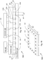
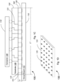
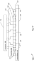
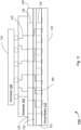
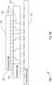
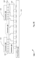
- FIGS. 1A , 1C , and 1E-3 are schematic cross-sectional views of different embodiments of a semiconductor device 100, in accordance with various embodiments.
- FIGS. 1B and 1D are top-front perspective views of a member 130, in accordance with various embodiments.
- the various components of semiconductor device 100 are schematically illustrated in FIGS. 1-3 , and that modifications to the various components, orientations, and other arrangements of semiconductor device 100 may be possible and in accordance with the various embodiments.
- Figs. 1-3 are described as separate embodiments for ease of description, a person of ordinary skill would understand that various modifications to each embodiment may be applied to other embodiments.
- the semiconductor device 100 includes a substrate 105.
- the substrate 105 is a supporting material (e.g., silicon, silicon dioxide, aluminum oxide, gallium, germanium, ceramics, organic structures, laminated organic structures, and/or any other material or combination of materials) upon which or within which elements or components (e.g., connectors 110, member 130, interconnects 125, or the like) of a semiconductor device 100 are fabricated or attached.
- elements or components e.g., connectors 110, member 130, interconnects 125, or the like
- the semiconductor device 100 includes one or more connectors 110.
- the one or more connectors 110 are one or more elements, components, accessories, mechanisms, devices, or the like capable of being connected (e.g., electrically coupled, attached, or the like) to the substrate 105.
- the one or more connectors 110 comprise a circuit board 115 (e.g., a printed circuit board (PCB)).
- the one or more connectors 110 e.g., one or more connectors 120
- the one or more connectors 110 comprise at least one of an optical connector, a high speed data connector, a high power connector, a backplane connector, or the like.
- the substrate 105 includes one or more layers.
- the layers can include one or more power planes, ground planes, other electrically conductive interconnect layers, non-conductive layers, redistribution layers, conductive structures, and other layers and structures.
- the layers may further include one or more layers configured to provide component interconnections.
- routing layers are layers of the substrate 105 through which interconnections may be established between components of the semiconductor device 100.
- the interconnections may be configured to connect (e.g., electrically connect) one or more connectors 120 to the circuit board 115. Connections may be routed, for example, through the substrate 105 via one or more interconnects 125.
- the interconnects 125 are one or more structures that couple (e.g., electrically couple or the like) two or more elements (e.g., substrate 105, connectors 110, member 130, or the like together) of the semiconductor device together.
- the interconnects 125 may include one or more copper or metal pads, copper or metal traces, copper or metal through-hole vias, copper or metal micro bumps, copper or metal solder balls, copper or metal posts or pillars, and/or other suitable interconnects.
- the interconnects 125 extend through the substrate 105 or are coupled to a surface of the substrate 105.
- traces 125a extend through the substrate 105 and are electrically coupled to solder balls 125b coupled to a surface of the substrate 105.
- the semiconductor device 100 further includes a member (e.g., a stiffener member, a stiffening member, a stiffener ring, a stiffening ring, or the like) 130.
- the stiffener member 130 is disposed between the substrate 105 and the connector 110.
- the member 130 is disposed between the substrate 105 and the printed circuit board 115.
- the member 130 is disposed between the substrate 105 and the connector(s) 120.
- a first member 130a is disposed between the substrate 105 and the printed circuit board 115 and a second member 130b is disposed between the substrate 105 and the connector(s) 120.
- the member 130 is configured to restrain to at least one of the substrate 105 or the connector 110.
- the member 130 controls or prevents in-plane thermal expansion or contraction along a length of the substrate 105 or connector 110.
- the member 130 controls or prevents the spread or reduction of the substrate 105 or connector 110 along a length L5 or a width W3 of the substrate 105 or connector 110.
- the member 130 controls or prevents out-of-plane (with respect to a plane extending along a length of the substrate) rotation of the substrate 105 or connector 110.
- the stiffener member 130 controls or prevents the substrate 105 or the connector 110 from curving or curling out-of-plane with respect to a plane extending along a length of the substrate.
- the member 130 provides control of the out-of-plane warpage to the extent of halving the out-of-plane warpage of an equivalent stiffener-free semiconductor device. This control is vital to the practical use of a component (e.g., semiconductor device 100, substrate 105, or connector 110, or the like), where a high degree of flatness is required. For example, a high degree of flatness is required for conditions such as component electrical test and component assembly.
- the member 130 may be in direct or indirect contact with the substrate 105 or the connector 110 to restrain at least one of the substrate 105 or the connector 110.
- the member 130 is configured to control or prevent the warpage or deformation of at least one of the substrate 105 or the connector 110. Warpage or deformation of at least one of the substrate 105 or the connector 110 may occur due to due to different construction materials used for the substrate 105 and the connector 110, due to a coefficient of thermal expansion mismatch between the substrate 105 and the connector 110, or the like.
- a semiconductor device that has warped or deformed more than a predetermined amount may be rendered useless because one or more interconnects 125 of the substrate 105 cannot connect to the one or more connectors 110.
- the member 130 works to restrain, prevent, or control at least one of substrate or connector from warping more than the predetermined amount and ensure that one or more interconnects 125 of the substrate 105 connect to the one or more connectors 110.
- the member 130 comprises one or more of a metal, ceramic, polymer, or any combination thereof. Even more specifically, the member 130 may comprise any combination of copper, aluminum, ceramic, steel, stainless steel, Teflon, silicon, or a polymer filled with silica or alumina, or the like.
- the member 130 is configured to have about a same or similar coefficient of thermal expansion as the substrate 105.
- the coefficient of thermal expansion measures the fractional change in size of an object per degree change in temperature at a constant pressure (e.g., atmospheric pressure at sea level or other constant pressure).
- a constant pressure e.g., atmospheric pressure at sea level or other constant pressure.
- the member 130 can have similar coefficient of thermal expansion properties (e.g., have similar expansion/contraction properties based on temperature) as the substrate. Having similar coefficient of thermal expansion properties between the substrate and the stiffener member helps to couple the member 130 to the substrate and further restrains the substrate 105 to reduce the warpage of the substrate 105 by helping control out-of-plane curling or curving of the substrate.
- the member 130 can also restrain the substrate 105 based on the stiffness or Young's Modulus of the member 130. A higher stiffness or modulus would further restrain the substrate 105 or connector 110 to reduce the warpage of the substrate 105.
- the effectiveness of the member 130 to restrain the substrate 105 or the connector 110 are 1) its stiffness which is a function of the Young's modulus, 2) its geometry (x, y, z dimensions described below with respect to Figs. 1A-3 ) and 3) its coefficient of thermal expansion. Each of these properties act together to restrain the substrate 105 or the connector 110.
- the member 130 additionally includes one or more vias 135.
- the one or more vias 135 may extend completely through a body 134 of the member 130 (e.g., a "through” via), may extend through a portion of the member 130 from one outer surface (e.g., a "blind” via), or may extend through a portion of the body 134 of the member 130 and be completely hidden from external view (e.g., a "buried” via), and/or the like.
- the one or more vias 135 might be filled, plated, or coated with an electrically conductive material.
- the electrically conductive material might include a metal such as copper, aluminum, gold, silver, tin, nickel, lead, or a combination of metals/alloys, or may be formed of other electrically conductive material or combination of electrically conductive materials.
- the one or more vias 135 are configured to form an electrical connection for an electrical signal to travel to or from the substrate 105 from or to the one or more connectors 110. In other words, the one or more vias 135 electrically couple the substrate 105 to the one or more connectors 110.
- the member 130 comprises at least two adjacent vias (e.g., vias 135a and 135b).
- a ratio between a distance D1 between an inside edge (or a center) of the at least two adjacent vias 135a and 135b and a width W1 of each via of the at least two adjacent vias 135a and 135b is at least 2:1.
- a ratio between a length L1 of the member 130 and a thickness T1 of the member 130 is equal or greater than 10:1.
- the one or more vias 135 may be electrically connected to the substrate 105, one or more connectors 110, and/or one or more interconnects 125 of the substrate 105 via one or more interconnects 140.
- the one or more interconnects 140 include, without limitation, one or more copper or metal pads, one or more copper or metal traces, one or more through-hole vias, micro bumps, one or more solder balls or bumps, one or more copper or metal posts or pillars, other suitable interconnects, combination of interconnects, or the like.
- FIGS. 1-3 various embodiments of the member 130 will be described with respect to FIGS. 1-3 .
- the member 130 of Figs. 1A-1F , 2A-2E , and 3 are described as separate embodiments for ease of description, a person of ordinary skill would understand that various modifications to the member 130 in each embodiment may be applied to other embodiments of the member 130.
- the member 130 is a ring (e.g., rectangular, circular, triangular, etc.) with an opening 150.
- One or more interconnects 125c may be disposed in the opening 150 to electrically couple the circuit board 115 to the substrate 105.
- the member 130 is located between the substrate 105 and the circuit board 115.
- the member 130 extends along a length and width or a perimeter of the substrate 105 or circuit board 115 as shown in FIGS. 1A and 1B .
- the member 130 applies restraint to a perimeter of the substrate 105 to prevent or control the warpage of the substrate 105.
- a first surface 155 of the member 130 pushes against a first surface 160 of the substrate 105 to prevent the substrate 105 from deforming or warping.
- the member 130 is a continuous layer with no openings except for the one or more vias 135.
- the member 130 has an area of a first surface 155 that is about or substantially a same area size (shown in FIG. 1C ) or a larger area size (shown in FIG. 1E ) as an area of a first surface 160 of the substrate 105 or a smaller area size (shown in FIG. 1F ) as an area of a first surface 160 of the substrate 105.
- the first surface 155 of the member 130 is about a same area size or a larger area size as an area of a first surface 160 of the substrate 105, the first surface 155 uniformly applies restraint across substantially an entire area of the first surface 160 of the substrate 105.
- uniformly applying restraint means that the member 130 about evenly controls (1) in-plane thermal expansion of the substrate 105 or connector 110 and (2) out-of-plane rotation of the substrate 105 or connector 110 about substantially an entire area of the first surface 160 of the substrate.
- the warpage or deformation of the substrate 105 may be prevented across the entire substrate 105 and not just at a perimeter of the substrate 105.
- a first surface 155 the member 130 pushes against a first surface 160 of the substrate 105 to prevent the substrate 105 from deforming or warping.
- the member 130 might have an area of a second surface 165 that is about or substantially a same area size as an area of a first surface 170 of the circuit board 115.
- the second surface 165 of the member 130 is about a same area size or a larger area size as an area of a first surface 170 of the circuit board 115, the second surface 165 of the member 130 uniformly applies restraint across substantially an entire area of the first surface 170 of the circuit board 115.
- uniformly applying restraint means that the member 130 about evenly controls (1) in-plane thermal expansion of the substrate 105 or connector 110 and (2) out-of-plane rotation of the substrate 105 or connector 110 about substantially an entire area of the first surface 170 of the circuit board 115.
- the warpage or deformation of the circuit board 115 may be prevented across the entire circuit board 115 and not just at a perimeter of the circuit board 115.
- a second surface 165 the member 130 pulls against a first surface 170 of the circuit board 115 to prevent the circuit board 115 from deforming or warping.
- the member 130 might have an area of a first surface 155 that is smaller than an area of a first surface 160 of the substrate 105.
- One or more interconnects 125 might be provided on an outer edge 157 of the member 130 between the circuit board 115 and the substrate 105.
- a length of the member 130 varies from the first surface 155 of the member 130 to the second surface 165 of the member 130.
- the length of the member 130 may vary based on a length L2 of the substrate and a length L3 of the circuit board 115.
- a length L2 of the first surface 155 of the member 130 might be about a same length as a length L2 of the first surface 160 of the substrate 105 while a length L3 of the second surface 165 of the member 130 might be about a same length as a length L3 of the first surface 170 of the circuit board 115.
- a length of the first surface 155 of the member 130 might be about a same length as a length of the first surface 160 of the substrate 105 while a length of the second surface 165 of the member 130 might be about a same length as a length of the first surface 170 of the circuit board 115.
- the member 130 in order to vary the length of the member 130, might include one or more sloped sidewalls 175.
- the first surface 155 of the member 130 uniformly applies restraint across substantially an entire area of the first surface 160 of the substrate 105 and the second surface 165 of the member 130 uniformly applies restraint across substantially an entire area of the first surface 170 of the circuit board 115.
- one or more members 130 may be selectively placed at different locations between the substrate 105 and the circuit board 115.
- the member 130 might be a ring 130c and have a portion 130d located towards a middle of the substrate 105, circuit board 115, the member 130b, or the like.
- One or more openings 180 between different portions of the member 130 might be used to add one or more additional connectors 110, interconnects 140, or other components.
- the member 130 is formed from one or more layers (e.g., layers 131, 132, and 133) as shown in FIG. 1I and 1J .
- the one or more layers might include a one or more redistribution layers 132 to route or reroute one or more electrical connections within the member 130 to different locations on the member 130.
- a redistribution layer 132 is needed when electrical connections within the substrate 105, member 130, and/or circuit board 115 are not aligned.
- a redistribution layer 132 having one or more interconnects 185 within the member 130 may be used to connect one or more vias 135 at different locations of the member 130, as shown in FIG. 1I .
- a redistribution layer 132 having one or more interconnects 185 within the member 130 may be used to connect one or more vias 135 with one or more interconnects 125 of the substrate 105 or the circuit board 115, as shown in FIG. 1J .
- the member 130 is located between a connector 120 and the substrate 105.
- the member 130 is a continuous layer with no openings except for the one or more vias 135.
- the member 130 could be a ring similar to the member 130 of FIGS. 1A and 1B .
- the member 130 might have an area of a first surface 155 that is about or substantially a same area size (shown in FIG. 2A ) or a larger area size as an area of a second surface 187 of the substrate 105.
- the first surface 155b of the member 130 When the first surface 155b of the member 130 is about a same area size or a larger area size as an area of a second surface 187 of the substrate 105, the first surface 155 uniformly applies restraint across substantially an entire area of the second surface 187 of the substrate 105. By uniformly applying restraint across the area of the second surface 187 of the substrate 105, the warpage or deformation of the substrate 105 may be prevented across the entire substrate 105 and not just at a perimeter of the substrate 105. In the case of FIG. 2A , the member 130 pulls a second surface 187 of the substrate 105 to prevent the substrate 105 from deforming or warping.
- the member 130 is located between a connector 120 and the substrate 105.
- the member 130 is a continuous layer with no openings except for the one or more vias 135.
- the member 130 might have an area of a second surface 190 that is about or substantially a same area size (shown in FIG. 2A ) or a larger area size as an area of a first surface 195 of the connector 120.
- the second surface 190 of the member 130 is about a same area size or a larger area size as an area of a first surface 195 of the connector 120, the second surface 190 uniformly applies restraint across substantially an entire area of the first surface 195 of the connector 120.
- the warpage or deformation of the connector 120 may be prevented across the entire substrate 105 and not just at a perimeter of the connector 120.
- the length of the member may vary based on a length of the substrate 105 and the connector 120.
- the member 130 is provided between the two or more connectors 120a and 120b and the substrate 105.
- the member 130 is a ring.
- a width W2a and W2b of the member 130 might vary based on a first surface (e.g., first surface 195a and 195b) of a connector 120 (e.g., connectors 120a and 120b).
- a width W2a of a first side of the member 130 is about a same width as a first surface 195a of the connector 120a while a width W2b of a second side opposite the first side of the member 130 is about a same width as a first surface 195b of the connector 120b.
- Width W2a and width W2a may be a same width or a different width depending on the widths of the first surfaces 195a and 195b of the connector 120.
- the member 130 is a continuous layer with no openings except for the one or more vias 135.
- the member 130 is provided between two or more connectors 120 (e.g., connectors 120a and 120b).
- the one or more vias 135 are selectively provided in locations where there are one or more connectors 120 and are not provided in locations where there are no connectors 120.
- the member 130 might have one or more openings selectively provided on the member 130.
- the one or more openings between different portions of the member 130 might be configured to surround one or more additional connectors 197, interconnects, or other components.
- the thickness of the member 130 may vary across a length L4 of the member 130.
- the member 130 might be thicker or thinner in a middle portion 198 of the member 130.
- the thickness of the middle portion 198 of the member 130 might be configured to be about flush or uniform with a second surface 199 of at least one of the one or more connectors 120.
- a first member 130 is located between the substrate and the circuit board 115 while a second member 130b is located between the substrate and the one or more connectors 120.
- the member 130 of Figs. 1A-1J , 2A-2F , and 3 are described as separate embodiments for ease of description, a person of ordinary skill would understand that various modifications to the member 130 in each embodiment may be applied to other embodiments of the member 130.
- the member 130 between the substrate 105 and the connector 120 may also have one or more redistribution layers similar to the embodiments described in FIGS. 1I and 1J .
- the member 130 is depicted as comprising a substantially rectangular or square cross-section, it should be appreciated that any shape or combination of shapes may be used for the member 130.
- the member 130 may comprise a tube shape (e.g., circular or elliptical cross section), a polygonal cross section, a triangular cross section, or the like.
- Fig. 4 is a flow diagram of a method 400 of manufacturing a semiconductor device 100, in accordance with various embodiments.
- the method 400 may begin, at block 405, by providing or forming a substrate.
- Forming the substrate may include, without limitation, various additive and/or subtractive manufacturing processes, as known to those skilled in the art.
- manufacturing techniques that are being developed and/or yet to be developed may be utilized to form the substrate.
- the method 400 is not limited to any particular method of manufacturing a particular substrate.
- the method 400 continues, at block 410, by providing or forming a connector.
- the connector may comprise at least one of a circuit board, optical connector, a high-speed data connector, a high-power connector, or a backplane connector, or the like.
- the method 400 continues, at block 415, by coupling a stiffening member to the substrate and the connector.
- the member is between the substrate and connector.
- the member includes one or more vias. The one or more vias extend through the member and electrically couple the substrate to the connector.
Landscapes
- Engineering & Computer Science (AREA)
- Microelectronics & Electronic Packaging (AREA)
- Structure Of Printed Boards (AREA)
- Combinations Of Printed Boards (AREA)
Abstract
Description
- A portion of the disclosure of this patent document contains material that is subject to copyright protection. The copyright owner has no objection to the facsimile reproduction by anyone of the patent document or the patent disclosure as it appears in the Patent and Trademark Office patent file or records, but otherwise reserves all copyright rights whatsoever.
- The present disclosure relates, in general, to methods, systems, and apparatuses for implementing a semiconductor package or a chip package, and more particularly to methods, systems, and apparatuses for implementing a semiconductor package or a chip package including a stiffener member with one or more vias.
- Traditional stiffener rings are purely mechanical and do not include any electrical features. As more connectors and connections are added to chip packages, the mechanical stiffener ring competes for space with the connectors and connections in the chip packages. Once the connectors and connections are added to the chip packages there is little to no space left for a mechanical stiffener ring. However, without a stiffener ring, chip package warpage can be high due to a coefficient of thermal expansion mismatch between a substrate and circuit board.
- Hence, there is a need for more robust and scalable solutions for implementing semiconductor packages and chip packages. Thus, methods, systems, and apparatuses for implementing semiconductor packages or chip packages including a stiffener member with one or more vias.
- A further understanding of the nature and advantages of particular embodiments may be realized by reference to the remaining portions of the specification and the drawings, in which like reference numerals are used to refer to similar components. In some instances, a sub-label is associated with a reference numeral to denote one of multiple similar components. When reference is made to a reference numeral without specification to an existing sub-label, it is intended to refer to all such multiple similar components.
-
FIGS. 1A ,1C , and1E-1J are schematic cross-sectional views of a semiconductor device with a member comprising one or more vias, in accordance with various embodiments; -
FIGS. 1B and1D are top-front perspective views of a member comprising one or more vias, in accordance with various embodiments; -
FIGS. 2A-2F are schematic cross-sectional views of a semiconductor device with a member comprising one or more vias, in accordance with various embodiments; -
FIG. 3 is a schematic cross-sectional view of a semiconductor device with a member comprising one or more vias, in accordance with various embodiments; and -
Fig. 4 is a flow diagram of a method of manufacturing a semiconductor device with a member comprising one or more vias, in accordance with various embodiments. - Various embodiments provide tools and techniques for implementing semiconductor packages or chip packages including a stiffener member with one or more vias.
- In a first aspect, an apparatus including a substrate is provided. A connector is coupled to the substrate. A member is disposed between the substrate and the connector. The member restrains at least one of the substrate or the connector. Additionally, a via extends through a body of the member. The via couples to the connector and to the substrate.
- In some embodiments, an area of a first surface of the member adjacent to a first surface of the substrate is characterized by about a same area size as an area of the first surface of the substrate. The member is configured to uniformly restrain the substrate across the area of the first surface of the substrate. In other cases, an area of a first surface of the member adjacent to a first surface of the substrate is smaller than a second surface of the member adjacent to a first surface of the connector.
- In various instances, the connector comprises a printed circuit board. An area of a second surface of the member adjacent to a first surface of the printed circuit board is characterized by about a same area size as an area of the first surface of the printed circuit board.
- In some embodiments, the connector comprises at least one of an optical connector, a high-speed data connector, a high-power connector, or a backplane connector, or the like. An area of a second surface of the member adjacent to a first surface of at least one of the optical connector, the high speed data connector, the high power connector, or the backplane connector is characterized by about a same area size or larger area size as an area of the first surface of at least one of the optical connector, the high speed data connector, the high power connector, or the backplane connector.
- In various cases, the member has about a same coefficient of thermal expansion as the substrate. The member comprises at least one of copper, aluminum, ceramic, steel, stainless steel, Teflon, silicon, or polymer, and the via comprises at least one of copper, aluminum, gold, silver, tin, nickel, or lead. The member comprises at least two adjacent vias. A ratio between a distance between the at least two adjacent vias and a width of each via of the at least two adjacent vias is at least 2:1. A ratio between a length of the member and a thickness of the member is equal or greater than 10:1.
- In another aspect, a semiconductor device comprises a substrate comprising an interconnect, a connector configured to couple to the interconnect of the substrate, and a member between the substrate and the connector. The member is configured to restrain at least one of the substrate or the connector. A via extends through the member and couples the interconnect of the substrate to the connector.
- In some instances, a first surface of the member adjacent to a first surface of the substrate uniformly restrains the substrate across the first surface of the substrate. In some instances, an area of a first surface of the member adjacent to a first surface of the substrate is larger than an area of the first surface of the substrate.
- In various embodiments, the connector comprises a printed circuit board. A second surface of the member adjacent to a first surface of the printed circuit board uniformly restrains the printed circuit board across the first surface of the printed circuit board. In other cases, the connector comprises at least one of an optical connector, a high-speed data connector, a high-power connector, or a backplane connector, or the like.
- In some cases, the via is located in a first layer of the member, and the member further comprises a second redistribution layer electrically coupled to the via.
- In yet another aspect, a method of manufacturing a semiconductor with a member is provided. The method includes providing a substrate and a connector. The method continues with coupling a member to the substrate and the connector. The member is between the substrate and the connector. The via extends through the member and electrically couples the substrate to the connector.
- In the following description, for the purposes of explanation, numerous details are set forth to provide a thorough understanding of the described embodiments. It will be apparent to one skilled in the art, however, that other embodiments may be practiced without some of these details. Several embodiments are described herein, and while various features are ascribed to different embodiments, it should be appreciated that the features described with respect to one embodiment may be incorporated with other embodiments as well. By the same token, however, no single feature or features of any described embodiment should be considered essential to every embodiment of the invention, as other embodiments of the invention may omit such features.
- When an element is referred to herein as being "connected" or "coupled" to another element, it is to be understood that the elements can be directly connected to the other element, or have intervening elements present between the elements. In contrast, when an element is referred to as being "directly connected" or "directly coupled" to another element, it should be understood that no intervening elements are present in the "direct" connection between the elements. However, the existence of a direct connection does not exclude other connections, in which intervening elements may be present.
- When an element is referred to herein as being "disposed" in some manner relative to another element (e.g., disposed on, disposed between, disposed under, disposed adjacent to, or disposed in some other relative manner), it is to be understood that the elements can be directly disposed relative to the other element (e.g., disposed directly on another element), or have intervening elements present between the elements. In contrast, when an element is referred to as being "disposed directly" relative to another element, it should be understood that no intervening elements are present in the "direct" example. However, the existence of a direct disposition does not exclude other examples in which intervening elements may be present.
- Likewise, when an element is referred to herein as being a "layer," it is to be understood that the layer can be a single layer or include multiple layers. For example, a conductive layer may comprise multiple different conductive materials or multiple layers of different conductive materials, and a dielectric layer may comprise multiple dielectric materials or multiple layers of dielectric materials. When a layer is described as being coupled or connected to another layer, it is to be understood that the coupled or connected layers may include intervening elements present between the coupled or connected layers. In contrast, when a layer is referred to as being "directly" connected or coupled to another layer, it should be understood that no intervening elements are present between the layers. However, the existence of directly coupled or connected layers does not exclude other connections in which intervening elements may be present.
- Moreover, the terms left, right, front, back, top, bottom, forward, reverse, clockwise and counterclockwise are used for purposes of explanation only and are not limited to any fixed direction or orientation. Rather, they are used merely to indicate relative locations and/or directions between various parts of an object and/or components.
- Furthermore, the methods and processes described herein may be described in a particular order for ease of description. However, it should be understood that, unless the context dictates otherwise, intervening processes may take place before and/or after any portion of the described process, and further various procedures may be reordered, added, and/or omitted in accordance with various embodiments.
- Unless otherwise indicated, all numbers used herein to express quantities, dimensions, and so forth should be understood as being modified in all instances by the term "about." The term "substantially" or "about" used herein refers to variations from the reference value or ratio of ± 10% or less (e.g., ± 10%, ± 5%, etc.), inclusive of the endpoints of the range.
- In this application, the use of the singular includes the plural unless specifically stated otherwise, and use of the terms "and" and "or" means "and/or" unless otherwise indicated. Moreover, the use of the terms "including" and "having," as well as other forms, such as "includes," "included," "has," "have," and "had," should be considered non-exclusive. Also, terms such as "element" or "component" encompass both elements and components comprising one unit and elements and components that comprise more than one unit, unless specifically stated otherwise.
- As used herein, the phrase "at least one of' preceding a series of items, with the term "and" or "or" to separate any of the items, modifies the list as a whole, rather than each member of the list (i.e., each item). The phrase "at least one of" does not require selection of at least one of each item listed; rather, the phrase allows a meaning that includes at least one of any one of the items, and/or at least one of any combination of the items. By way of example, the phrases "at least one of A, B, and C" or "at least one of A, B, or C" each refer to only A, only B, or only C; and/or any combination of A, B, and C. In instances where it is intended that a selection be of "at least one of each of A, B, and C," or alternatively, "at least one of A, at least one of B, and at least one of C," it is expressly described as such.
- In conventional semiconductor or chip packages, stiffener rings are purely mechanical with no electrical features. However, as chip packages become more complex, the stiffener ring competes for space with connectors within the chip package.
- The proposed embodiments may be a semiconductor or chip module (e.g., integrated circuit (IC), chip, or other semiconductor device) that provides a stiffener member with one or more vias. By implementing a stiffener member with one or more vias, the stiffener member can be configured to provide one or more electrical connections between the one or more connectors and a substrate of the semiconductor or chip module. Thus, this improved stiffener member provides electrical connections between the substrate and the one or more connectors while still controlling warpage between the substrate and the one or more connectors.
-
FIGS. 1A ,1C , and1E-3 are schematic cross-sectional views of different embodiments of asemiconductor device 100, in accordance with various embodiments.FIGS. 1B and1D are top-front perspective views of amember 130, in accordance with various embodiments. It should be noted that the various components ofsemiconductor device 100 are schematically illustrated inFIGS. 1-3 , and that modifications to the various components, orientations, and other arrangements ofsemiconductor device 100 may be possible and in accordance with the various embodiments. In addition, althoughFigs. 1-3 are described as separate embodiments for ease of description, a person of ordinary skill would understand that various modifications to each embodiment may be applied to other embodiments. - In various embodiments, the
semiconductor device 100 includes asubstrate 105. Thesubstrate 105 is a supporting material (e.g., silicon, silicon dioxide, aluminum oxide, gallium, germanium, ceramics, organic structures, laminated organic structures, and/or any other material or combination of materials) upon which or within which elements or components (e.g.,connectors 110,member 130, interconnects 125, or the like) of asemiconductor device 100 are fabricated or attached. - In some instances, the
semiconductor device 100 includes one ormore connectors 110. The one ormore connectors 110 are one or more elements, components, accessories, mechanisms, devices, or the like capable of being connected (e.g., electrically coupled, attached, or the like) to thesubstrate 105. In some cases, the one ormore connectors 110 comprise a circuit board 115 (e.g., a printed circuit board (PCB)). Additionally or alternatively, the one or more connectors 110 (e.g., one or more connectors 120) comprise at least one of an optical connector, a high speed data connector, a high power connector, a backplane connector, or the like. - In various cases, the
substrate 105 includes one or more layers. The layers can include one or more power planes, ground planes, other electrically conductive interconnect layers, non-conductive layers, redistribution layers, conductive structures, and other layers and structures. The layers may further include one or more layers configured to provide component interconnections. For example, routing layers are layers of thesubstrate 105 through which interconnections may be established between components of thesemiconductor device 100. In a non-limiting example, the interconnections may be configured to connect (e.g., electrically connect) one ormore connectors 120 to thecircuit board 115. Connections may be routed, for example, through thesubstrate 105 via one ormore interconnects 125. Theinterconnects 125 are one or more structures that couple (e.g., electrically couple or the like) two or more elements (e.g.,substrate 105,connectors 110,member 130, or the like together) of the semiconductor device together. Theinterconnects 125 may include one or more copper or metal pads, copper or metal traces, copper or metal through-hole vias, copper or metal micro bumps, copper or metal solder balls, copper or metal posts or pillars, and/or other suitable interconnects. - In some cases, the
interconnects 125 extend through thesubstrate 105 or are coupled to a surface of thesubstrate 105. In a non-limiting example, as shown inFIG. 1A andFIG. 2B ,traces 125a extend through thesubstrate 105 and are electrically coupled tosolder balls 125b coupled to a surface of thesubstrate 105. - In various embodiments, the
semiconductor device 100 further includes a member (e.g., a stiffener member, a stiffening member, a stiffener ring, a stiffening ring, or the like) 130. Thestiffener member 130 is disposed between thesubstrate 105 and theconnector 110. In the case ofFIGS. 1A-1I , themember 130 is disposed between thesubstrate 105 and the printedcircuit board 115. Alternatively, as shown inFIGS. 2A-2F , themember 130 is disposed between thesubstrate 105 and the connector(s) 120. Alternatively, as shown in FIGS. 3A, afirst member 130a is disposed between thesubstrate 105 and the printedcircuit board 115 and asecond member 130b is disposed between thesubstrate 105 and the connector(s) 120. - The
member 130 is configured to restrain to at least one of thesubstrate 105 or theconnector 110. For example, in order to restrain at least one of thesubstrate 105 or theconnector 110, themember 130 controls or prevents in-plane thermal expansion or contraction along a length of thesubstrate 105 orconnector 110. In other words, themember 130 controls or prevents the spread or reduction of thesubstrate 105 orconnector 110 along a length L5 or a width W3 of thesubstrate 105 orconnector 110. Additionally, in order to restrain at least one of thesubstrate 105 or theconnector 110, themember 130 controls or prevents out-of-plane (with respect to a plane extending along a length of the substrate) rotation of thesubstrate 105 orconnector 110. In other words, thestiffener member 130 controls or prevents thesubstrate 105 or theconnector 110 from curving or curling out-of-plane with respect to a plane extending along a length of the substrate. In some cases, themember 130 provides control of the out-of-plane warpage to the extent of halving the out-of-plane warpage of an equivalent stiffener-free semiconductor device. This control is vital to the practical use of a component (e.g.,semiconductor device 100,substrate 105, orconnector 110, or the like), where a high degree of flatness is required. For example, a high degree of flatness is required for conditions such as component electrical test and component assembly. - The
member 130 may be in direct or indirect contact with thesubstrate 105 or theconnector 110 to restrain at least one of thesubstrate 105 or theconnector 110. By restraining at least one of thesubstrate 105 or theconnector 110, themember 130 is configured to control or prevent the warpage or deformation of at least one of thesubstrate 105 or theconnector 110. Warpage or deformation of at least one of thesubstrate 105 or theconnector 110 may occur due to due to different construction materials used for thesubstrate 105 and theconnector 110, due to a coefficient of thermal expansion mismatch between thesubstrate 105 and theconnector 110, or the like. A semiconductor device that has warped or deformed more than a predetermined amount may be rendered useless because one ormore interconnects 125 of thesubstrate 105 cannot connect to the one ormore connectors 110. Themember 130 works to restrain, prevent, or control at least one of substrate or connector from warping more than the predetermined amount and ensure that one ormore interconnects 125 of thesubstrate 105 connect to the one ormore connectors 110. - In some embodiments, the
member 130 comprises one or more of a metal, ceramic, polymer, or any combination thereof. Even more specifically, themember 130 may comprise any combination of copper, aluminum, ceramic, steel, stainless steel, Teflon, silicon, or a polymer filled with silica or alumina, or the like. - The
member 130 is configured to have about a same or similar coefficient of thermal expansion as thesubstrate 105. The coefficient of thermal expansion measures the fractional change in size of an object per degree change in temperature at a constant pressure (e.g., atmospheric pressure at sea level or other constant pressure). By forming themember 130 from a material having about the same or similar coefficient of thermal expansion as thesubstrate 105, themember 130 can have similar coefficient of thermal expansion properties (e.g., have similar expansion/contraction properties based on temperature) as the substrate. Having similar coefficient of thermal expansion properties between the substrate and the stiffener member helps to couple themember 130 to the substrate and further restrains thesubstrate 105 to reduce the warpage of thesubstrate 105 by helping control out-of-plane curling or curving of the substrate. - The
member 130 can also restrain thesubstrate 105 based on the stiffness or Young's Modulus of themember 130. A higher stiffness or modulus would further restrain thesubstrate 105 orconnector 110 to reduce the warpage of thesubstrate 105. The effectiveness of themember 130 to restrain thesubstrate 105 or theconnector 110 are 1) its stiffness which is a function of the Young's modulus, 2) its geometry (x, y, z dimensions described below with respect toFigs. 1A-3 ) and 3) its coefficient of thermal expansion. Each of these properties act together to restrain thesubstrate 105 or theconnector 110. - The
member 130 additionally includes one ormore vias 135. The one ormore vias 135 may extend completely through abody 134 of the member 130 (e.g., a "through" via), may extend through a portion of themember 130 from one outer surface (e.g., a "blind" via), or may extend through a portion of thebody 134 of themember 130 and be completely hidden from external view (e.g., a "buried" via), and/or the like. The one ormore vias 135 might be filled, plated, or coated with an electrically conductive material. The electrically conductive material might include a metal such as copper, aluminum, gold, silver, tin, nickel, lead, or a combination of metals/alloys, or may be formed of other electrically conductive material or combination of electrically conductive materials. The one ormore vias 135 are configured to form an electrical connection for an electrical signal to travel to or from thesubstrate 105 from or to the one ormore connectors 110. In other words, the one ormore vias 135 electrically couple thesubstrate 105 to the one ormore connectors 110. - In some cases, as shown in
FIG. 1A , themember 130 comprises at least two adjacent vias (e.g., vias 135a and 135b). A ratio between a distance D1 between an inside edge (or a center) of the at least twoadjacent vias adjacent vias member 130 is maximized. In some cases, as shown inFIG. 1C , a ratio between a length L1 of themember 130 and a thickness T1 of themember 130 is equal or greater than 10:1. By making themember 130 as thin as possible, cross-talk between the adjacent vias is minimized while usage of space within themember 130 is maximized. - The one or
more vias 135 may be electrically connected to thesubstrate 105, one ormore connectors 110, and/or one ormore interconnects 125 of thesubstrate 105 via one ormore interconnects 140. The one ormore interconnects 140 include, without limitation, one or more copper or metal pads, one or more copper or metal traces, one or more through-hole vias, micro bumps, one or more solder balls or bumps, one or more copper or metal posts or pillars, other suitable interconnects, combination of interconnects, or the like. - Now various embodiments of the
member 130 will be described with respect toFIGS. 1-3 . Although themember 130 ofFigs. 1A-1F ,2A-2E , and3 are described as separate embodiments for ease of description, a person of ordinary skill would understand that various modifications to themember 130 in each embodiment may be applied to other embodiments of themember 130. - Turning to
FIG. 1A and 1B , themember 130 is a ring (e.g., rectangular, circular, triangular, etc.) with anopening 150. One ormore interconnects 125c may be disposed in theopening 150 to electrically couple thecircuit board 115 to thesubstrate 105. Themember 130 is located between thesubstrate 105 and thecircuit board 115. Themember 130 extends along a length and width or a perimeter of thesubstrate 105 orcircuit board 115 as shown inFIGS. 1A and 1B . When themember 130 is a ring, themember 130 applies restraint to a perimeter of thesubstrate 105 to prevent or control the warpage of thesubstrate 105. In the case ofFIG. 1A , afirst surface 155 of themember 130 pushes against afirst surface 160 of thesubstrate 105 to prevent thesubstrate 105 from deforming or warping. - In
FIGS. 1C-1F , themember 130 is a continuous layer with no openings except for the one ormore vias 135. Themember 130 has an area of afirst surface 155 that is about or substantially a same area size (shown inFIG. 1C ) or a larger area size (shown inFIG. 1E ) as an area of afirst surface 160 of thesubstrate 105 or a smaller area size (shown inFIG. 1F ) as an area of afirst surface 160 of thesubstrate 105. When thefirst surface 155 of themember 130 is about a same area size or a larger area size as an area of afirst surface 160 of thesubstrate 105, thefirst surface 155 uniformly applies restraint across substantially an entire area of thefirst surface 160 of thesubstrate 105. As used herein, uniformly applying restraint means that themember 130 about evenly controls (1) in-plane thermal expansion of thesubstrate 105 orconnector 110 and (2) out-of-plane rotation of thesubstrate 105 orconnector 110 about substantially an entire area of thefirst surface 160 of the substrate. By uniformly applying restraint across the area of thefirst surface 160 of thesubstrate 105, the warpage or deformation of thesubstrate 105 may be prevented across theentire substrate 105 and not just at a perimeter of thesubstrate 105. In the case ofFIG. 1C and1E , afirst surface 155 themember 130 pushes against afirst surface 160 of thesubstrate 105 to prevent thesubstrate 105 from deforming or warping. - In some cases, as shown in
FIG. 1E , themember 130 might have an area of asecond surface 165 that is about or substantially a same area size as an area of afirst surface 170 of thecircuit board 115. When thesecond surface 165 of themember 130 is about a same area size or a larger area size as an area of afirst surface 170 of thecircuit board 115, thesecond surface 165 of themember 130 uniformly applies restraint across substantially an entire area of thefirst surface 170 of thecircuit board 115. As used herein, uniformly applying restraint means that themember 130 about evenly controls (1) in-plane thermal expansion of thesubstrate 105 orconnector 110 and (2) out-of-plane rotation of thesubstrate 105 orconnector 110 about substantially an entire area of thefirst surface 170 of thecircuit board 115. By uniformly applying restraint across the area of thefirst surface 170 of thecircuit board 115, the warpage or deformation of thecircuit board 115 may be prevented across theentire circuit board 115 and not just at a perimeter of thecircuit board 115. In the case ofFIG. 1C and1E , asecond surface 165 themember 130 pulls against afirst surface 170 of thecircuit board 115 to prevent thecircuit board 115 from deforming or warping. - In some cases, as shown in
FIG. 1F , themember 130 might have an area of afirst surface 155 that is smaller than an area of afirst surface 160 of thesubstrate 105. One ormore interconnects 125 might be provided on anouter edge 157 of themember 130 between thecircuit board 115 and thesubstrate 105. - In some embodiments, a length of the
member 130 varies from thefirst surface 155 of themember 130 to thesecond surface 165 of themember 130. The length of themember 130 may vary based on a length L2 of the substrate and a length L3 of thecircuit board 115. In a non-limiting example, as shown inFIG. 1G , if thesubstrate 105 is smaller than thecircuit board 115, then a length L2 of thefirst surface 155 of themember 130 might be about a same length as a length L2 of thefirst surface 160 of thesubstrate 105 while a length L3 of thesecond surface 165 of themember 130 might be about a same length as a length L3 of thefirst surface 170 of thecircuit board 115. Alternatively, if thesubstrate 105 is smaller than thecircuit board 115, then a length of thefirst surface 155 of themember 130 might be about a same length as a length of thefirst surface 160 of thesubstrate 105 while a length of thesecond surface 165 of themember 130 might be about a same length as a length of thefirst surface 170 of thecircuit board 115. In some cases, in order to vary the length of themember 130, themember 130 might include one or moresloped sidewalls 175. By varying the length of themember 130 based on the lengths of thesubstrate 105 and thecircuit board 115, thefirst surface 155 of themember 130 uniformly applies restraint across substantially an entire area of thefirst surface 160 of thesubstrate 105 and thesecond surface 165 of themember 130 uniformly applies restraint across substantially an entire area of thefirst surface 170 of thecircuit board 115. - As shown in
FIG. 1H , one ormore members 130 may be selectively placed at different locations between thesubstrate 105 and thecircuit board 115. In a non-limiting example, themember 130 might be aring 130c and have aportion 130d located towards a middle of thesubstrate 105,circuit board 115, themember 130b, or the like. One ormore openings 180 between different portions of themember 130 might be used to add one or moreadditional connectors 110, interconnects 140, or other components. - In some cases, the
member 130 is formed from one or more layers (e.g., layers 131, 132, and 133) as shown inFIG. 1I and1J . The one or more layers might include a one ormore redistribution layers 132 to route or reroute one or more electrical connections within themember 130 to different locations on themember 130. Aredistribution layer 132 is needed when electrical connections within thesubstrate 105,member 130, and/orcircuit board 115 are not aligned. In a non-limiting example, aredistribution layer 132 having one ormore interconnects 185 within themember 130 may be used to connect one ormore vias 135 at different locations of themember 130, as shown inFIG. 1I . Alternatively, aredistribution layer 132 having one ormore interconnects 185 within themember 130 may be used to connect one ormore vias 135 with one ormore interconnects 125 of thesubstrate 105 or thecircuit board 115, as shown inFIG. 1J . - Turning to
FIG. 2A , themember 130 is located between aconnector 120 and thesubstrate 105. In this case, themember 130 is a continuous layer with no openings except for the one ormore vias 135. However, themember 130 could be a ring similar to themember 130 ofFIGS. 1A and 1B . Themember 130 might have an area of afirst surface 155 that is about or substantially a same area size (shown inFIG. 2A ) or a larger area size as an area of asecond surface 187 of thesubstrate 105. When the first surface 155b of themember 130 is about a same area size or a larger area size as an area of asecond surface 187 of thesubstrate 105, thefirst surface 155 uniformly applies restraint across substantially an entire area of thesecond surface 187 of thesubstrate 105. By uniformly applying restraint across the area of thesecond surface 187 of thesubstrate 105, the warpage or deformation of thesubstrate 105 may be prevented across theentire substrate 105 and not just at a perimeter of thesubstrate 105. In the case ofFIG. 2A , themember 130 pulls asecond surface 187 of thesubstrate 105 to prevent thesubstrate 105 from deforming or warping. - Turning to
FIG. 2B , themember 130 is located between aconnector 120 and thesubstrate 105. In this case, themember 130 is a continuous layer with no openings except for the one ormore vias 135. Themember 130 might have an area of asecond surface 190 that is about or substantially a same area size (shown inFIG. 2A ) or a larger area size as an area of afirst surface 195 of theconnector 120. When thesecond surface 190 of themember 130 is about a same area size or a larger area size as an area of afirst surface 195 of theconnector 120, thesecond surface 190 uniformly applies restraint across substantially an entire area of thefirst surface 195 of theconnector 120. By uniformly applying restraint across the area of thefirst surface 195 of theconnector 120, the warpage or deformation of theconnector 120 may be prevented across theentire substrate 105 and not just at a perimeter of theconnector 120. In some cases, similar toFIG. 1F , the length of the member may vary based on a length of thesubstrate 105 and theconnector 120. - In some cases, as shown in
FIG. 2C , there are two or more connectors 120 (e.g.,connectors member 130 is provided between the two ormore connectors substrate 105. In the case ofFIG. 2C , themember 130 is a ring. A width W2a and W2b of themember 130 might vary based on a first surface (e.g.,first surface connectors member 130 is about a same width as afirst surface 195a of theconnector 120a while a width W2b of a second side opposite the first side of themember 130 is about a same width as afirst surface 195b of theconnector 120b. Width W2a and width W2a may be a same width or a different width depending on the widths of thefirst surfaces connector 120. - In
FIG. 2D , themember 130 is a continuous layer with no openings except for the one ormore vias 135. Themember 130 is provided between two or more connectors 120 (e.g.,connectors more vias 135 are selectively provided in locations where there are one ormore connectors 120 and are not provided in locations where there are noconnectors 120. - As shown in
FIG. 2E , themember 130 might have one or more openings selectively provided on themember 130. The one or more openings between different portions of themember 130 might be configured to surround one or moreadditional connectors 197, interconnects, or other components. - In various embodiments, as shown in
FIG. 2F , the thickness of themember 130 may vary across a length L4 of themember 130. In a non-limiting example, themember 130 might be thicker or thinner in amiddle portion 198 of themember 130. In some cases, the thickness of themiddle portion 198 of themember 130 might be configured to be about flush or uniform with asecond surface 199 of at least one of the one ormore connectors 120. - Turning to
FIG. 3 , twomembers first member 130 is located between the substrate and thecircuit board 115 while asecond member 130b is located between the substrate and the one ormore connectors 120. - It should be noted that although the
member 130 ofFigs. 1A-1J ,2A-2F , and3 are described as separate embodiments for ease of description, a person of ordinary skill would understand that various modifications to themember 130 in each embodiment may be applied to other embodiments of themember 130. In a non-limiting example, themember 130 between thesubstrate 105 and theconnector 120 may also have one or more redistribution layers similar to the embodiments described inFIGS. 1I and1J . Additionally, although themember 130 is depicted as comprising a substantially rectangular or square cross-section, it should be appreciated that any shape or combination of shapes may be used for themember 130. In some non-limiting examples, themember 130 may comprise a tube shape (e.g., circular or elliptical cross section), a polygonal cross section, a triangular cross section, or the like. -
Fig. 4 is a flow diagram of amethod 400 of manufacturing asemiconductor device 100, in accordance with various embodiments. Themethod 400 may begin, atblock 405, by providing or forming a substrate. Forming the substrate may include, without limitation, various additive and/or subtractive manufacturing processes, as known to those skilled in the art. In further examples, manufacturing techniques that are being developed and/or yet to be developed may be utilized to form the substrate. Thus, it is to be understood that themethod 400 is not limited to any particular method of manufacturing a particular substrate. - The
method 400 continues, atblock 410, by providing or forming a connector. The connector may comprise at least one of a circuit board, optical connector, a high-speed data connector, a high-power connector, or a backplane connector, or the like. - The
method 400 continues, atblock 415, by coupling a stiffening member to the substrate and the connector. The member is between the substrate and connector. The member includes one or more vias. The one or more vias extend through the member and electrically couple the substrate to the connector. - The techniques and processes described above with respect to various embodiments may be used to manufacture the
semiconductor devices 100 ofFIGS. 1-3 , and/or components thereof, as described herein. - While some features and aspects have been described with respect to the embodiments, one skilled in the art will recognize that numerous modifications are possible. For example, the methods and processes described herein may be implemented using hardware components, custom integrated circuits (ICs), programmable logic, and/or any combination thereof. Further, while various methods and processes described herein may be described with respect to particular structural and/or functional components for ease of description, methods provided by various embodiments are not limited to any particular structural and/or functional architecture but instead can be implemented in any suitable hardware configuration. Similarly, while some functionality is ascribed to one or more system components, unless the context dictates otherwise, this functionality can be distributed among various other system components in accordance with the several embodiments.
- Moreover, while the procedures of the methods and processes described herein are described in a particular order for ease of description, unless the context dictates otherwise, various procedures may be reordered, added, and/or omitted in accordance with various embodiments. Moreover, the procedures described with respect to one method or process may be incorporated within other described methods or processes; likewise, system components described according to a particular structural architecture and/or with respect to one system may be organized in alternative structural architectures and/or incorporated within other described systems. Hence, while various embodiments are described with or without some features for ease of description and to illustrate aspects of those embodiments, the various components and/or features described herein with respect to a particular embodiment can be substituted, added and/or subtracted from among other described embodiments, unless the context dictates otherwise. Consequently, although several embodiments are described above, it will be appreciated that the invention is intended to cover all modifications and equivalents within the scope of the following claims.
Claims (15)
- An apparatus (100) comprising:a substrate (105);a connector (110) coupled to the substrate (105); anda member (130) disposed between the substrate (105) and the connector (110) and configured to restrain at least one of the substrate (105) or the connector (110), the member (130) comprising a via (135), the via (135) being coupled to the connector (110) and to the substrate (105).
- The apparatus (100) of claim 1, wherein an area of a first surface of the member (130) adjacent to a first surface (160) of the substrate (105) is characterized by about a same area size as an area of the first surface (160) of the substrate (105).
- The apparatus (100) of claim 1 or 2, wherein the member (130) is configured to uniformly restrain the substrate (105) across the area of the first surface (160) of the substrate (105).
- The apparatus (100) of any of claims 1 to 3, wherein an area of a first surface of the member (130) adjacent to a first surface (160) of the substrate (105) is smaller than a second surface of the member (130) adjacent to a first surface of the connector (110).
- The apparatus (100) of any of claims 1 to 4, wherein the connector (110) comprises a printed circuit board.
- The apparatus (100) of claim 5, wherein an area of a second surface of the member (130) adjacent to a first surface of the printed circuit board is characterized by about a same area size as an area of the first surface of the printed circuit board.
- The apparatus (100) of any of claims 1 to 6, wherein the connector (110) comprises at least one of an optical connector, a high-speed data connector, a high-power connector, or a backplane connector.
- The apparatus (100) of claim 7, wherein an area of a second surface of the member (130) adjacent to a first surface of the connector (110) is characterized by about a same area size or larger area size as an area of the first surface of the connector (110).
- The apparatus (100) of any of claims 1 to 8, comprising at least one of the following features:
wherein the member (130) has a about a same coefficient of thermal expansion as the substrate (105);wherein the member (130) comprises at least two adjacent vias (135), and wherein a ratio between a distance between the at least two adjacent vias (135) and a width of each via (135) of the at least two adjacent vias (135) is at least 2:1;wherein a ratio between a length of the member (130) and a thickness of the member (130) is equal or greater than 10:1;wherein the member (130) comprises at least one of copper, aluminum, ceramic, steel, stainless steel, Teflon, silicon, or polymer, and wherein the via (135) comprises at least one of copper, aluminum, gold, silver, tin, nickel, or lead. - A semiconductor device (100) comprising:a substrate (105) comprising an interconnect;a connector (110) configured to couple to the interconnect of the substrate (105); anda member (130) between the substrate (105) and the connector (110) and configured to restrain at least one of the substrate (105) or the connector (110), the member (130) comprising a via (135) coupling the interconnect of the substrate (105) to the connector (110).
- The semiconductor device (100) of claim 10, comprising at least one of the following features:
wherein a first surface of the member (130) adjacent to a first surface (160) of the substrate (105) uniformly restrains the substrate (105) across the first surface (160) of the substrate (105);
wherein an area of a first surface of the member (130) adjacent to a first surface (160) of the substrate (105) is larger than an area of the first surface (160) of the substrate (105). - The semiconductor device (100) of claim 10 or 11, wherein the connector (110) comprises a printed circuit board.
- The semiconductor device (100) of claim 12, wherein a second surface of the member (130) adjacent to a first surface (160) of the printed circuit board uniformly restrains the printed circuit board across the first surface of the printed circuit board.
- The semiconductor device (100) of any of claims 10 to 13, comprising at least one of the following features:
wherein the connector (110) comprises at least one of an optical connector, a high-speed data connector, a high-power connector, or a backplane connector;
wherein the via (135) is located in a first layer of the member (130), and the member (130) further comprises a second redistribution layer electrically coupled to the via (135). - A method comprising:providing a substrate (105);providing a connector (110); andcoupling a member (130) to the substrate (105) and the connector (110), the member (130) configured to restrain at least one of the substrate (105) or the connector (110), wherein the member (130) is between the substrate (105) and the connector (110) and comprises a via (135), the via (135) being coupled to the connector (110) and to the substrate (105).
Applications Claiming Priority (1)
| Application Number | Priority Date | Filing Date | Title |
|---|---|---|---|
| US18/360,522 US20250038085A1 (en) | 2023-07-27 | 2023-07-27 | Stiffener member with one or more vias |
Publications (1)
| Publication Number | Publication Date |
|---|---|
| EP4498767A1 true EP4498767A1 (en) | 2025-01-29 |
Family
ID=92043260
Family Applications (1)
| Application Number | Title | Priority Date | Filing Date |
|---|---|---|---|
| EP24190960.5A Pending EP4498767A1 (en) | 2023-07-27 | 2024-07-25 | Stiffener member with one or more vias |
Country Status (3)
| Country | Link |
|---|---|
| US (1) | US20250038085A1 (en) |
| EP (1) | EP4498767A1 (en) |
| CN (1) | CN119381353A (en) |
Citations (6)
| Publication number | Priority date | Publication date | Assignee | Title |
|---|---|---|---|---|
| US6137164A (en) * | 1998-03-16 | 2000-10-24 | Texas Instruments Incorporated | Thin stacked integrated circuit device |
| US6373717B1 (en) * | 1999-07-02 | 2002-04-16 | International Business Machines Corporation | Electronic package with high density interconnect layer |
| US6399892B1 (en) * | 2000-09-19 | 2002-06-04 | International Business Machines Corporation | CTE compensated chip interposer |
| US20060202322A1 (en) * | 2003-09-24 | 2006-09-14 | Ibiden Co., Ltd. | Interposer, and multilayer printed wiring board |
| US8289728B2 (en) * | 2009-10-02 | 2012-10-16 | Fujitsu Limited | Interconnect board, printed circuit board unit, and method |
| US20230197676A1 (en) * | 2021-12-21 | 2023-06-22 | Intel Corporation | Quasi-monolithic integrated packaging architecture with mid-die serializer/deserializer |
Family Cites Families (5)
| Publication number | Priority date | Publication date | Assignee | Title |
|---|---|---|---|---|
| WO2017171893A1 (en) * | 2016-04-02 | 2017-10-05 | Intel Corporation | Systems, methods, and apparatuses for implementing an organic stiffener with an emi shield for rf integration |
| CN118316415A (en) * | 2019-04-05 | 2024-07-09 | 株式会社村田制作所 | Transverse excited film bulk acoustic resonator package and method |
| US12394720B2 (en) * | 2022-08-16 | 2025-08-19 | Taiwan Semiconductor Manufacturing Company Limited | Semiconductor package including reinforcement structure and methods of forming the same |
| US12137516B2 (en) * | 2022-10-06 | 2024-11-05 | Avago Technologies International Sales Pte. Limited | Package with self shielding |
| US20240203822A1 (en) * | 2022-12-18 | 2024-06-20 | International Business Machines Corporation | Thermal expansion matched chip module with integrated liquid cooling |
-
2023
- 2023-07-27 US US18/360,522 patent/US20250038085A1/en active Pending
-
2024
- 2024-06-04 CN CN202410715104.4A patent/CN119381353A/en active Pending
- 2024-07-25 EP EP24190960.5A patent/EP4498767A1/en active Pending
Patent Citations (6)
| Publication number | Priority date | Publication date | Assignee | Title |
|---|---|---|---|---|
| US6137164A (en) * | 1998-03-16 | 2000-10-24 | Texas Instruments Incorporated | Thin stacked integrated circuit device |
| US6373717B1 (en) * | 1999-07-02 | 2002-04-16 | International Business Machines Corporation | Electronic package with high density interconnect layer |
| US6399892B1 (en) * | 2000-09-19 | 2002-06-04 | International Business Machines Corporation | CTE compensated chip interposer |
| US20060202322A1 (en) * | 2003-09-24 | 2006-09-14 | Ibiden Co., Ltd. | Interposer, and multilayer printed wiring board |
| US8289728B2 (en) * | 2009-10-02 | 2012-10-16 | Fujitsu Limited | Interconnect board, printed circuit board unit, and method |
| US20230197676A1 (en) * | 2021-12-21 | 2023-06-22 | Intel Corporation | Quasi-monolithic integrated packaging architecture with mid-die serializer/deserializer |
Also Published As
| Publication number | Publication date |
|---|---|
| CN119381353A (en) | 2025-01-28 |
| US20250038085A1 (en) | 2025-01-30 |
Similar Documents
| Publication | Publication Date | Title |
|---|---|---|
| US8014154B2 (en) | Circuit substrate for preventing warpage and package using the same | |
| US9516740B2 (en) | Electronic component embedded substrate and method for manufacturing electronic component embedded substrate | |
| US6756663B2 (en) | Semiconductor device including wiring board with three dimensional wiring pattern | |
| US9723729B2 (en) | Printed wiring board | |
| US6816385B1 (en) | Compliant laminate connector | |
| US6310392B1 (en) | Stacked micro ball grid array packages | |
| JP7091801B2 (en) | Through Silicon Via and its manufacturing method, and mounting board | |
| US6077766A (en) | Variable thickness pads on a substrate surface | |
| EP2026641A2 (en) | Oblong peripheral solder ball pads on a printed circuit board for mounting a ball grid array package | |
| US20050189640A1 (en) | Interconnect system without through-holes | |
| JP5384700B2 (en) | Device mounting structure and device mounting structure manufacturing method | |
| KR20060064651A (en) | Integrated electronic chip and interconnect device and process for making the same | |
| CN101911291A (en) | Ball grid array package with traces for plating pads under the chip | |
| KR20140021910A (en) | Core substrate and printed circuit board using the same | |
| KR20080028821A (en) | Circuit board for preventing warpage and manufacturing method thereof | |
| JP7690974B2 (en) | Wiring board and method for manufacturing same | |
| US20050104221A1 (en) | High wireability microvia substrate | |
| US20170196096A1 (en) | Printed wiring board and method for manufacturing printed wiring board | |
| US20090283303A1 (en) | Package substrate having landless conductive traces | |
| EP3038150B1 (en) | Chip scale package with flexible interconnect | |
| US20250038085A1 (en) | Stiffener member with one or more vias | |
| US20160212854A1 (en) | Printed wiring board | |
| US12218044B2 (en) | Semiconductor device | |
| US20250336830A1 (en) | Die-to-die links using substrate and method of making | |
| US20250336789A1 (en) | Posts having multiple widths |
Legal Events
| Date | Code | Title | Description |
|---|---|---|---|
| PUAI | Public reference made under article 153(3) epc to a published international application that has entered the european phase |
Free format text: ORIGINAL CODE: 0009012 |
|
| STAA | Information on the status of an ep patent application or granted ep patent |
Free format text: STATUS: THE APPLICATION HAS BEEN PUBLISHED |
|
| AK | Designated contracting states |
Kind code of ref document: A1 Designated state(s): AL AT BE BG CH CY CZ DE DK EE ES FI FR GB GR HR HU IE IS IT LI LT LU LV MC ME MK MT NL NO PL PT RO RS SE SI SK SM TR |
|
| STAA | Information on the status of an ep patent application or granted ep patent |
Free format text: STATUS: REQUEST FOR EXAMINATION WAS MADE |
|
| 17P | Request for examination filed |
Effective date: 20250710 |
|
| STAA | Information on the status of an ep patent application or granted ep patent |
Free format text: STATUS: EXAMINATION IS IN PROGRESS |
|
| 17Q | First examination report despatched |
Effective date: 20250827 |