EP4498591A1 - Power conversion device - Google Patents
Power conversion device Download PDFInfo
- Publication number
- EP4498591A1 EP4498591A1 EP23795846.7A EP23795846A EP4498591A1 EP 4498591 A1 EP4498591 A1 EP 4498591A1 EP 23795846 A EP23795846 A EP 23795846A EP 4498591 A1 EP4498591 A1 EP 4498591A1
- Authority
- EP
- European Patent Office
- Prior art keywords
- main body
- body portion
- opposing surface
- positive electrode
- busbar
- Prior art date
- Legal status (The legal status is an assumption and is not a legal conclusion. Google has not performed a legal analysis and makes no representation as to the accuracy of the status listed.)
- Granted
Links
Images




Classifications
-
- H—ELECTRICITY
- H02—GENERATION; CONVERSION OR DISTRIBUTION OF ELECTRIC POWER
- H02M—APPARATUS FOR CONVERSION BETWEEN AC AND AC, BETWEEN AC AND DC, OR BETWEEN DC AND DC, AND FOR USE WITH MAINS OR SIMILAR POWER SUPPLY SYSTEMS; CONVERSION OF DC OR AC INPUT POWER INTO SURGE OUTPUT POWER; CONTROL OR REGULATION THEREOF
- H02M7/00—Conversion of AC power input into DC power output; Conversion of DC power input into AC power output
- H02M7/003—Constructional details, e.g. physical layout, assembly, wiring or busbar connections
-
- H—ELECTRICITY
- H01—ELECTRIC ELEMENTS
- H01G—CAPACITORS; CAPACITORS, RECTIFIERS, DETECTORS, SWITCHING DEVICES, LIGHT-SENSITIVE OR TEMPERATURE-SENSITIVE DEVICES OF THE ELECTROLYTIC TYPE
- H01G4/00—Fixed capacitors; Processes of their manufacture
- H01G4/002—Details
- H01G4/228—Terminals
-
- H—ELECTRICITY
- H01—ELECTRIC ELEMENTS
- H01G—CAPACITORS; CAPACITORS, RECTIFIERS, DETECTORS, SWITCHING DEVICES, LIGHT-SENSITIVE OR TEMPERATURE-SENSITIVE DEVICES OF THE ELECTROLYTIC TYPE
- H01G4/00—Fixed capacitors; Processes of their manufacture
- H01G4/40—Structural combinations of fixed capacitors with other electric elements, the structure mainly consisting of a capacitor, e.g. RC combinations
-
- H—ELECTRICITY
- H05—ELECTRIC TECHNIQUES NOT OTHERWISE PROVIDED FOR
- H05K—PRINTED CIRCUITS; CASINGS OR CONSTRUCTIONAL DETAILS OF ELECTRIC APPARATUS; MANUFACTURE OF ASSEMBLAGES OF ELECTRICAL COMPONENTS
- H05K7/00—Constructional details common to different types of electric apparatus
- H05K7/14—Mounting supporting structure in casing or on frame or rack
- H05K7/1422—Printed circuit boards receptacles, e.g. stacked structures, electronic circuit modules or box like frames
- H05K7/1427—Housings
- H05K7/1432—Housings specially adapted for power drive units or power converters
- H05K7/14329—Housings specially adapted for power drive units or power converters specially adapted for the configuration of power bus bars
-
- H—ELECTRICITY
- H10—SEMICONDUCTOR DEVICES; ELECTRIC SOLID-STATE DEVICES NOT OTHERWISE PROVIDED FOR
- H10W—GENERIC PACKAGES, INTERCONNECTIONS, CONNECTORS OR OTHER CONSTRUCTIONAL DETAILS OF DEVICES COVERED BY CLASS H10
- H10W90/00—Package configurations
- H10W90/701—Package configurations characterised by the relative positions of pads or connectors relative to package parts
-
- H—ELECTRICITY
- H02—GENERATION; CONVERSION OR DISTRIBUTION OF ELECTRIC POWER
- H02M—APPARATUS FOR CONVERSION BETWEEN AC AND AC, BETWEEN AC AND DC, OR BETWEEN DC AND DC, AND FOR USE WITH MAINS OR SIMILAR POWER SUPPLY SYSTEMS; CONVERSION OF DC OR AC INPUT POWER INTO SURGE OUTPUT POWER; CONTROL OR REGULATION THEREOF
- H02M3/00—Conversion of DC power input into DC power output
- H02M3/003—Constructional details, e.g. physical layout, assembly, wiring or busbar connections
-
- H—ELECTRICITY
- H10—SEMICONDUCTOR DEVICES; ELECTRIC SOLID-STATE DEVICES NOT OTHERWISE PROVIDED FOR
- H10W—GENERIC PACKAGES, INTERCONNECTIONS, CONNECTORS OR OTHER CONSTRUCTIONAL DETAILS OF DEVICES COVERED BY CLASS H10
- H10W90/00—Package configurations
Definitions
- the present disclosure relates to a power conversion device.
- Patent Document 1 discloses a power conversion device in which a positive electrode side conductor and a negative electrode side conductor each connected to a capacitor are stacked in a laminate structure sandwiching an insulating layer therebetween.
- the positive electrode side conductor and the negative electrode side conductor as connection conductors both have a flat plate shape and are opposed in a state of being parallel to each other with the insulating layer therebetween.
- Patent Document 2 discloses a semiconductor device including a main terminal group as a connection conductor configured by continuously arranging three or more main terminals.
- a main terminal as a collector terminal connected to a collector electrode of a semiconductor chip and a main terminal as an emitter terminal connected to an emitter electrode of the semiconductor chip are alternately arranged in a state of being adjacent to each other.
- the magnetic fluxes generated in the main terminals may not smoothly cancel each other.
- the main terminal may be increased in size and weight.
- the present disclosure has been made to solve the above problem, and an object of the present disclosure is to provide a power conversion device that can reduce parasitic inductance generated in a connection conductor while suppressing an increase in size and weight of the connection conductor.
- a power conversion device includes a capacitor to which DC power is supplied, a power module configured to convert a DC voltage from the capacitor into an AC voltage and output the AC voltage, and a connection conductor including a positive electrode-side busbar configured to connect the capacitor and a P-type terminal of the power module and a negative electrode-side busbar having a shape identical to a shape of the positive electrode-side busbar, symmetrically arranged side by side with the positive electrode-side busbar in pairs with a gap therebetween, and configured to connect the capacitor and an N-type terminal of the power module.
- the positive electrode-side busbar includes a first main body portion including a first bottom surface abutting on the P-type terminal and a first opposing surface rising from the first bottom surface and a first cutout portion disposed in at least part of the first main body portion on a side opposite to the first bottom surface and the first opposing surface.
- the negative electrode-side busbar includes a second main body portion including a second bottom surface abutting on the N-type terminal and a second opposing surface rising from the second bottom surface and disposed in parallel to and opposed to the first opposing surface with a gap therebetween and a second cutout portion disposed in part of the second main body portion on a side opposite to the second bottom surface and the second opposing surface.
- a power conversion device that can reduce parasitic inductance generated in a connection conductor while suppressing an increase in size and weight of the connection conductor can be provided.
- the power conversion device is a device that converts DC power into AC power, converts AC power into DC power, or converts DC power into DC power having a different potential.
- Examples of the power conversion device of the present embodiment include an inverter used in a system of a power plant or the like, an inverter used for driving an electric motor of an electric vehicle, or the like.
- an inverter for controlling an electric motor (motor) will be described as an example of the power conversion device.
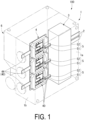
- a power conversion device 100 includes a casing 1, an external input conductor 2, a capacitor 3, a power conversion unit 4, a cooling device 6, and a connection conductor 5.
- the casing 1 forms an outer shell of the power conversion device 100.
- the casing 1 in the present embodiment is made of a metal such as aluminum, a synthetic resin, or the like, and has a rectangular parallelepiped shape.
- the casing 1 includes two side surfaces arranged so as to be back-to-back with each other.
- a side surface opposing one side is referred to as an "input-side side surface 1a", and a side surface opposing the other side is referred to as an “output-side side surface 1b”.
- the external input conductor 2 for inputting DC power is led out from the input-side side surface 1a.
- the external input conductors 2 are a pair of electrical conductors (busbars) that supply DC power supplied from a DC power supply or the like provided outside the power conversion device 100 to the capacitor 3.
- the external input conductor 2 in the present embodiment is made of a metal including copper or the like.
- One end of the external input conductor 2 is connected to the capacitor 3, and the other end of the external input conductor 2 extends in a direction intersecting the input-side side surface 1a of the casing 1.
- the capacitor 3 is a smoothing capacitor for storing electric charge input from the external input conductor 2 and suppressing voltage fluctuation associated with power conversion.
- the DC voltage smoothed by suppressing ripples through the capacitor 3 is supplied to the power conversion unit 4.
- the power conversion unit 4 converts the voltage input from the capacitor 3.
- the power conversion unit 4 in the present embodiment includes three power modules 40 responsible for outputs for the U phase, the V phase, and the W phase, respectively.
- the power module 40 is a device that converts input power and outputs the converted power.
- the power module 40 in the present embodiment constitutes a part of the power conversion unit 4.
- the power module 40 includes a base plate 41, a circuit board 42, a main terminal portion 43, an external output conductor 44, and a reinforcing portion 45.
- the base plate 41 is a member having a flat plate shape.
- the base plate 41 includes a main surface 41a and a back surface 41b located on the back side of the main surface 41a.
- the main surface 41a and the back surface 41b of the base plate 41 are back-to-back in a state of being parallel to each other.
- the back surface 41b of the base plate 41 is fixed to, for example, the cooling device 6 with a bonding material or the like (not illustrated) therebetween.
- the base plate 41 in the present embodiment is made of, for example, copper.
- the base plate 41 may be made of a metal other than copper.
- the circuit board 42 includes an insulating plate 420, a front surface pattern 421, a power semiconductor element 422, and a back surface pattern (not illustrated for convenience of illustration).
- the insulating plate 420 has a flat plate shape.
- the insulating plate 420 includes a first surface 420a and a second surface 420b located on the back side of the first surface 420a.
- first surface 420a and the second surface 420b of the insulating plate 420 are back-to-back in a state of being parallel to each other.
- a back surface pattern which is a pattern of copper foil or the like, is formed on the second surface 420b of the insulating plate 420.
- the back surface pattern is fixed to the center of the main surface 41a of the base plate 41 with a bonding material or the like (not illustrated) therebetween.
- the insulating plate 420 is made of an insulating material such as ceramic.
- paper phenol, paper epoxy, glass composite, glass epoxy, glass polyimide, fluororesin, or the like can be used as the insulating material forming the insulating plate 420.
- the front surface pattern 421 is a pattern of copper foil or the like formed on the first surface 420a of the insulating plate 420 and extending in a planar shape.
- the front surface pattern 421 is formed by, for example, being fixed to the first surface 420a of the insulating plate 420 by adhesion or the like and then being etched or the like.
- a plurality of the front surface patterns 421 are disposed on the first surface 420a of the insulating plate 420.
- the plurality of front surface patterns 421 are arranged adjacent to each other with a gap therebetween in a direction in which the insulating plate 420 extends.
- first front surface pattern 421a a first front surface pattern 421a
- second front surface pattern 421b a second front surface pattern 421c
- third front surface pattern 421c a third front surface pattern
- the main terminal portion 43 (P-type terminal 431) as a positive electrode for inputting a direct current is connected to the first front surface pattern 421a.
- the main terminal portion 43 (N-type terminal 432) as a negative electrode for outputting a direct current is connected to the second front surface pattern 421b.
- the first front surface pattern 421a corresponds to an inlet portion of a loop between P and N formed in the front surface pattern 421, and the second front surface pattern 421b corresponds to an outlet portion of the loop between P and N.
- the external output conductor 44 for outputting an alternating current converted by the power semiconductor element 422 to a load such as a motor (not illustrated) provided outside the power conversion device 100 is connected to the third front surface pattern 421c.
- the power semiconductor element 422 is a circuit element that converts power by a switching operation of turning on and off a voltage or a current.
- the power semiconductor element 422 is, for example, a switching element such as an IGBT or a MOSFET.
- six power semiconductor elements 422 are connected to the front surface pattern 421 on the circuit board 42.
- the six power semiconductor elements 422 in the present embodiment include three first power semiconductor elements 422a and three second power semiconductor elements 422b.
- the first power semiconductor element 422a is connected to the first front surface pattern 421a.
- the second power semiconductor element 422b is connected to the third front surface pattern 421c.
- the power semiconductor element 422 When the power semiconductor element 422 is the IGBT, the power semiconductor element 422 includes an input surface on which an input terminal corresponding to a collector is formed, an output surface on which an output terminal corresponding to an emitter is formed, and a gate corresponding to a control signal input terminal for controlling switching of the power semiconductor element 422.
- the input surface of the power semiconductor element 422 is electrically connected to the front surface pattern 421 with a bonding material or the like (not illustrated) therebetween.
- one end of a bonding wire (not illustrated) as a conducting wire is electrically connected to the output surface of the power semiconductor element 422.
- the input surface of the first power semiconductor element 422a is connected to the first front surface pattern 421a.
- the other end of the bonding wire connected to the output surface of the first power semiconductor element 422a is connected to the third front surface pattern 421c.
- the input surface of the second power semiconductor element 422b is connected to the third front surface pattern 421c.
- the other end of the bonding wire connected to the output surface of the second power semiconductor element 422b is connected to the second front surface pattern 421b.
- DC power is input to the input terminal of the first power semiconductor element 422a through the first front surface pattern 421a, and the input DC power is converted into AC power by the first power semiconductor element 422a.
- the converted AC power is output from an output terminal (not illustrated) in the first power semiconductor element 422a to the third front surface pattern 421c through a bonding wire.
- AC power is input to the input terminal of the second power semiconductor element 422b through the third front surface pattern 421c, and the input AC power is converted into DC power by the second power semiconductor element 422b.
- the converted DC power is output from an output terminal (not illustrated) in the second power semiconductor element 422b to the second front surface pattern 421b through a bonding wire.
- a control signal generated by a control unit (not illustrated) provided outside the circuit board 42 is input to the power semiconductor element 422.
- the power semiconductor element 422 performs switching in accordance with the control signal.
- the power semiconductor element 422 When the power semiconductor element 422 is the MOSFET, the power semiconductor element 422 includes an input surface corresponding to a drain, an output surface corresponding to a source, and a gate corresponding to a control signal input terminal.
- solder a sintered material (powder of a metal or the like), or the like can be adopted as the above-described bonding material used for bonding the base plate 41 and the back surface pattern formed on the second surface 420b of the insulating plate 420 to each other, bonding the power semiconductor element 422 and the front surface pattern 421 to each other, and bonding the back surface 41b of the base plate 41 and the cooling device 6 to each other.
- the main terminal portion 43 is an electric conductor (busbar) that exchanges DC power between the capacitor 3 and the circuit board 42.
- the main terminal portion 43 is made of a metal such as copper.
- the main terminal portion 43 includes the P-type terminal 431 as the positive electrode and the N-type terminal 432 as the negative electrode.
- the P-type terminal 431 and the N-type terminal 432 are arranged side by side with a gap therebetween.
- the N-type terminal 432 is arranged side by side with the P-type terminal 431 with a gap therebetween.
- the P-type terminal 431 and the N-type terminal 432 have the same size and shape.
- the term "same” in the present embodiment refers to a substantially same state, and a slight manufacturing error and a design tolerance are allowed.
- the P-type terminal 431 includes one end portion 431b connected to the first front surface pattern 421a, and the other end portion 431a which extends integrally with the one end portion 431b from the one end portion 431b and into which a direct current from the positive electrode of the capacitor 3 flows.
- the other end portion 431a of the P-type terminal 431 has a flat plate shape.
- the N-type terminal 432 includes one end portion 432b connected to the second front surface pattern 421b and the other end portion 432a extending integrally with the one end portion 432b from the one end portion 432b and allowing a direct current to flow out toward the negative electrode of the capacitor 3.
- the other end portion 432a of the N-type terminal 432 has a flat plate shape.
- the external output conductor 44 is an electrical conductor (busbar) for outputting the AC power converted by the power semiconductor element 422 to the outside of the power conversion device 100.
- the external output conductor 44 is made of a metal including copper or the like.
- One end of the external output conductor 44 is connected to the third front surface pattern 421c on the circuit board 42.
- the other end of the external output conductor 44 extends outward beyond the output-side side surface 1b of the casing 1.
- a wiring (not illustrated) for current output connected to a load such as a motor is connected to the other end of the external output conductor 44, for example.
- the reinforcing portion 45 is a member that is fixed to the main surface 41a of the base plate 41 and mechanically reinforces the main terminal portion 43 and the external output conductor 44.
- the reinforcing portion 45 is made of a synthetic resin material or the like.
- the reinforcing portion 45 covers the main terminal portion 43 and the external output conductor 44 from the outside and surrounds the circuit board 42 from the outside.
- the reinforcing portion 45 forms a case surrounding the circuit board 42 from the periphery in a direction along the main surface 41a of the base plate 41.
- the reinforcing portion 45 defines a space in which the circuit board 42 is accommodated together with the base plate 41.
- the reinforcing portion 45 is fixed to the first surface 420a of the base plate 41 with an adhesive or the like therebetween.
- an insulating material such as polyphenylene sulfide (PPS) can be adopted as the synthetic resin material for the reinforcing portion 45 in the present embodiment.
- PPS polyphenylene sulfide
- An insulating material other than PPS may be used for the reinforcing portion 45.
- the space defined by the reinforcing portion 45 and the base plate 41 is referred to as a potting space P.
- a liquid potting material (not illustrated) is poured (potting) into the potting space P from the outside, and the front surface pattern 421 on the circuit board 42 and the power semiconductor element 422 each exposed to the potting space P are sealed.
- the potting material poured into the potting space P is cured over a predetermined time, and electrically insulates the front surface pattern 421 on the circuit board 42 and the power semiconductor element 422 from a space outside the power module 40.
- potting material in the present embodiment for example, silicone gel, an epoxy resin, or the like is adopted.
- a synthetic resin other than the silicone gel and the epoxy resin may be used as the potting material.
- the cooling device 6 is a device that mainly cools the power module 40 of the power conversion unit 4.
- the cooling device 6 is provided so as to be stacked on the casing 1, and is fixed to and integrated with the casing 1.
- a liquid refrigerant such as water is introduced into the cooling device 6 from the outside.
- the liquid refrigerant exchanges heat with the power module 40 and is heated, thereby cooling the power module 40.
- connection conductor 5 that relays DC power between the capacitor 3 and the power module 40 will be described with reference to FIGS. 2 and 3 .
- connection conductor 5 is an electrical conductor (busbar) made of a metal including copper or the like.
- connection conductors 5 are arranged at intervals so as to correspond to the power modules 40. respectively.
- Each connection conductor 5 includes a positive electrode-side busbar 51 and a negative electrode-side busbar 52.
- the positive electrode-side busbar 51 is a current path that connects the positive electrode of the capacitor 3 and the power module 40.
- the negative electrode-side busbar 52 is a current path that connects the negative electrode of the capacitor 3 and the power module 40.
- the positive electrode-side busbar 51 and the negative electrode-side busbar 52 are arranged side by side at an interval.
- One end of each of the positive electrode-side busbar 51 and the negative electrode-side busbar 52 is connected to the capacitor 3.
- connection states between the positive electrode-side busbar 51 and the capacitor 3 and between the negative electrode-side busbar 52 and the capacitor 3 are omitted.
- the other end of the positive electrode-side busbar 51 is connected to the P-type terminal 431 in the power module 40.
- the other end of the negative electrode-side busbar 52 is connected to the N-type terminal 432 of the power module 40.
- the positive electrode-side busbar 51 and the negative electrode-side busbar 52 have the same size and shape.
- the positive electrode-side busbar 51 and the negative electrode-side busbar 52 in the present embodiment are symmetrically arranged side by side to form a pair.
- an interval generated between the positive electrode-side busbar 51 and the negative electrode-side busbar 52 by being arranged side by side is referred to as a "gap G".
- the negative electrode-side busbar 52 is arranged side by side with the positive electrode-side busbar 51 with the gap G therebetween.
- the gap G in the present embodiment has the same dimension as a gap G formed between the P-type terminal 431 and the N-type terminal 432.
- An insulation distance (a spatial distance and a creepage distance) is secured in the gap G so that a current flowing through the positive electrode-side busbar 51 does not flow to the negative electrode-side busbar 52 or a current flowing through the negative electrode-side busbar 52 does not flow to the positive electrode-side busbar 51.
- the insulation distance in the present embodiment is desirably, for example, 1 mm or more and 10 mm or less.
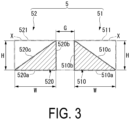
- the positive electrode-side busbar 51 includes a first main body portion 510 and a first cutout portion 511.
- the first main body portion 510 in the present embodiment has a columnar shape extending in one direction between the capacitor 3 and the power module 40.
- the first main body portion 510 includes a first bottom surface 510a abutting on the P-type terminal 431 and a first opposing surface 510b rising from the first bottom surface 510a.
- the first bottom surface 510a and the first opposing surface 510b are perpendicular to each other.
- perpendicular in the present embodiment refers to a substantially perpendicular state, and a slight manufacturing error and a design tolerance are allowed.
- the first bottom surface 510a is integrally connected to the P-type terminal 431 by, for example, welding.
- the first cutout portion 511 is disposed in the first main body portion 510 on a side opposite to the first bottom surface 510a and the first opposing surface 510b.
- the first cutout portion 511 is disposed so as to cut out, in a triangular prism shape in the direction in which the base material X extends, one corner disposed on a side opposite to the first bottom surface 510a forming a bottom surface of a base material X and the first opposing surface 510b forming a side surface of the base material X among four corners of the base material X forming a quadrangular prism shape forming the first main body portion 510.
- a first inclined surface 510c that connects an end edge of the first bottom surface 510a and an end edge of the first opposing surface 510b to each other is formed in the first main body portion 510 by the first cutout portion 511.
- the first main body portion 510 is formed in a triangular prism shape having a right-angled triangular cross section by the first bottom surface 510a, the first opposing surface 510b, and the first inclined surface 510c included in the first main body portion 510.
- the "cross section" in the present embodiment means a plane obtained by cutting the first main body portion 510 along a plane orthogonal to the direction in which the first main body portion 510 extends.
- the negative electrode-side busbar 52 includes a second main body portion 520 and a second cutout portion 521.
- the second main body portion 520 in the present embodiment has a columnar shape extending in the same direction as the direction in which the first main body portion 510 extends between the capacitor 3 and the power module 40.
- the second main body portion 520 includes a second bottom surface 520a abutting on the N-type terminal 432 and a second opposing surface 520b rising from the second bottom surface 520a.
- the second bottom surface 520a and the first opposing surface 510b are perpendicular to each other.
- the second bottom surface 520a is integrally connected to the P-type terminal 431 by, for example, welding.
- the second opposing surface 520b is disposed in parallel to and opposed to the first opposing surface 510b with the gap G therebetween.
- the second cutout portion 521 is disposed in the second main body portion 520 on a side opposite to the second bottom surface 520a and the second opposing surface 520b.
- the second cutout portion 521 is disposed so as to cut out, in a triangular prism shape in the direction in which the base material X extends, one corner disposed on a side opposite to the second bottom surface 520a forming a bottom surface of a base material X and the second opposing surface 520b forming a side surface of the base material X among four corners of the base material X forming a quadrangular prism shape forming the second main body portion 520.
- a second inclined surface 520c that connects an end edge of the second bottom surface 520a and an end edge of the second opposing surface 520b to each other is formed in the second main body portion 520 by the second cutout portion 521.
- the second main body portion 520 is formed in a triangular prism shape having a right-angled triangular cross section by the second bottom surface 520a, the second opposing surface 520b, and the second inclined surface 520c included in the second main body portion 520.
- a dimension of the first opposing surface 510b and the second opposing surface 520b in the direction perpendicular to the first bottom surface 510a and the second bottom surface 520a, respectively, is H
- a dimension of the first bottom surface 510a and the second bottom surface 520a in the direction in which the first opposing surface 510b and the second opposing surface 520b are opposed is W
- the following expression (i) is established.
- a current input from the capacitor 3 to the front surface pattern 421 through the positive electrode-side busbar 51 and the P-type terminal 431 each as the positive electrode is converted by the power semiconductor element 422 and then used for rotation of a motor or the like (load) provided outside the power conversion device 100 through the external output conductor 44.
- the current used for the rotation of the motor or the like flows into the front surface pattern 421 again through the external output conductor 44, is converted by the power semiconductor element 422, and then returns to the capacitor 3 through the N-type terminal 432 and the negative electrode-side busbar 52 each as the negative electrode.
- the positive electrode-side busbar 51 and the negative electrode-side busbar 52 are arranged side by side with the gap G therebetween, and a flow direction of the current flowing through the positive electrode-side busbar 51 and a flow direction of the current flowing through the negative electrode-side busbar 52 are opposite to each other.
- the above-described configuration can secure larger areas of the first opposing surface 510b of the first main body portion 510 and the second opposing surface 520b of the second main body portion 520 by the first cutout portion 511 disposed in the first main body portion 510 and the second cutout portion 521 disposed in the second main body portion 520 as compared with, for example, a connection conductor 5 having a flat plate shape (quadrangular prism).
- opposing areas of the first main body portion 510 and the second main body portion 520 can be increased.
- parasitic inductance generated in the connection conductor 5 can be reduced while suppressing an increase in size and weight of the connection conductor 5.
- the configuration of the first main body portion 510 and the second main body portion 520 formed in the triangular prism shape having the right-angled triangular cross section has been described.
- a configuration is not limited to this configuration.
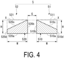
- the positive electrode-side busbar 51 and the negative electrode-side busbar 52 may have configurations as illustrated in FIG. 4 , for example.
- the positive electrode-side busbar 51 includes the first main body portion 510 and the first cutout portion 511.
- the first main body portion 510 includes the first bottom surface 510a abutting on the P-type terminal 431, the first opposing surface 510b rising from the first bottom surface 510a, and a first side surface 510d rising from the first bottom surface 510a and opposing a side opposite to the first opposing surface 510b in a state of being parallel to the first opposing surface 510b.
- the first cutout portion 511 is disposed in the first main body portion 510 on a side opposite to the first bottom surface 510a and the first opposing surface 510b.
- the first cutout portion 511 is disposed so as to cut out, in a triangular prism shape in the direction in which the base material X extends, one corner disposed on a side opposite to the first bottom surface 510a forming a bottom surface of a base material X and the first opposing surface 510b forming a side surface of the base material X among four corners of the base material X forming a quadrangular prism shape forming the first main body portion 510.
- a first inclined surface 510c that connects an end edge of the first opposing surface 510b and an end edge of the first side surface 510d to each other is formed in the first main body portion 510 by the first cutout portion 511.
- the first main body portion 510 in this configuration is formed in a quadrangular prism shape having a trapezoidal cross section by the first bottom surface 510a, the first opposing surface 510b, the first side surface 510d, and the first inclined surface 510c included in the first main body portion 510.
- the first side surface 510d corresponds to an upper base of the trapezoidal shape
- the first opposing surface 510b corresponds to a lower base of the trapezoidal shape
- the negative electrode-side busbar 52 includes a second main body portion 520 and a second cutout portion 521.
- the second main body portion 520 includes the second bottom surface 520a abutting on the N-type terminal 432, the second opposing surface 520b rising from the second bottom surface 520a, and a second side surface 520d rising from the second bottom surface 520a and opposing a side opposite to the second opposing surface 520b in a state of being parallel to the second opposing surface 520b.
- the second opposing surface 520b is disposed in parallel to and opposed to the first opposing surface 510b with the gap G therebetween.
- the second cutout portion 521 is disposed in the second main body portion 520 on a side opposite to the second bottom surface 520a and the second opposing surface 520b.
- the second cutout portion 521 is disposed so as to cut out, in a triangular prism shape in the direction in which the base material X extends, one corner disposed on a side opposite to the second bottom surface 520a forming a bottom surface of a base material X and the second opposing surface 520b forming a side surface of the base material X among four corners of the base material X forming a quadrangular prism shape forming the second main body portion 520.
- a second inclined surface 520c that connects an end edge of the second opposing surface 520b and an end edge of the second side surface 520d to each other is formed in the second main body portion 520 by the second cutout portion 521.
- the second main body portion 520 in this configuration is formed in a quadrangular prism shape having a trapezoidal cross section by the second bottom surface 520a, the second opposing surface 520b, the second side surface 520d, and the second inclined surface 520c included in the second main body portion 520.
- the second side surface 520d corresponds to an upper base of the trapezoidal shape
- the second opposing surface 520b corresponds to a lower base of the trapezoidal shape
- the positive electrode-side busbar 51 and the negative electrode-side busbar 52 may have configurations as illustrated in FIG. 5 , for example.
- the positive electrode-side busbar 51 includes the first main body portion 510 and the first cutout portion 511.
- the first main body portion 510 includes the first bottom surface 510a abutting on the P-type terminal 431, the first opposing surface 510b rising from the first bottom surface 510a, the first side surface 510d rising from the first bottom surface 510a and opposing a side opposite to the first opposing surface 510b in a state of being parallel to the first opposing surface 510b, and a first upper surface 510e that is connected to the first opposing surface 510b and faces a side opposite to the first bottom surface 510a in a state of being parallel to the first bottom surface 510a.
- the first cutout portion 511 is disposed in the first main body portion 510 on a side opposite to the first bottom surface 510a and the first opposing surface 510b.
- the first cutout portion 511 is disposed so as to cut out, in a triangular prism shape in the direction in which the base material X extends, one corner disposed on a side opposite to the first bottom surface 510a forming a bottom surface of a base material X and the first opposing surface 510b forming a side surface of the base material X among four corners of the base material X forming a quadrangular prism shape forming the first main body portion 510.
- a first inclined surface 510c that connects an end edge of the first upper surface 510e and an end edge of the first side surface 510d to each other is formed in the first main body portion 510 by the first cutout portion 511.
- the first main body portion 510 in this configuration is formed in a pentagonal prism shape having a pentagonal cross section by the first bottom surface 510a, the first opposing surface 510b, the first side surface 510d, the upper surface 510e, and the first inclined surface 510c included in the first main body portion 510.
- the negative electrode-side busbar 52 includes a second main body portion 520 and a second cutout portion 521.
- the second main body portion 520 includes the second bottom surface 520a abutting on the N-type terminal 432, the second opposing surface 520b rising from the second bottom surface 520a, the second side surface 520d rising from the second bottom surface 520a and opposing a side opposite to the second opposing surface 520b in a state of being parallel to the second opposing surface 520b, and a second upper surface 520e that is connected to the second opposing surface 520b and faces a side opposite to the second bottom surface 520a in a state of being parallel to the second bottom surface 520a.
- the second opposing surface 520b is disposed in parallel to and opposed to the first opposing surface 510b with the gap G therebetween.
- the second cutout portion 521 is disposed in the second main body portion 520 on a side opposite to the second bottom surface 520a and the second opposing surface 520b.
- the second cutout portion 521 is disposed so as to cut out, in a triangular prism shape in the direction in which the base material X extends, one corner disposed on a side opposite to the second bottom surface 520a forming a bottom surface of a base material X and the second opposing surface 520b forming a side surface of the base material X among four corners of the base material X forming a quadrangular prism shape forming the second main body portion 520.
- a second inclined surface 520c that connects an end edge of the second upper surface 520e and an end edge of the second side surface 520d to each other is formed in the second main body portion 520 by the second cutout portion 521.
- the second main body portion 520 in this configuration is formed in a pentagonal prism shape having a pentagonal cross section by the second bottom surface 520a, the second opposing surface 520b, the second side surface 520d, the second upper surface 520e, and the second inclined surface 520c included in the second main body portion 520.
- the positive electrode-side busbar 51 and the negative electrode-side busbar 52 may have configurations as illustrated in FIG. 6 , for example.
- the positive electrode-side busbar 51 includes the first main body portion 510 and the first cutout portion 511.
- the first main body portion 510 includes the first bottom surface 510a abutting on the P-type terminal 431, the first opposing surface 510b rising from the first bottom surface 510a, the first side surface 510d rising from the first bottom surface 510a and opposing a side opposite to the first opposing surface 510b in a state of being parallel to the first opposing surface 510b, and the first upper surface 510e that is connected to the first opposing surface 510b and faces a side opposite to the first bottom surface 510a in a state of being parallel to the first bottom surface 510a.
- the first cutout portion 511 is disposed in the first main body portion 510 on a side opposite to the first bottom surface 510a and the first opposing surface 510b.
- the first cutout portion 511 is disposed so as to cut out, in a quadrangular prism shape in the direction in which the base material X extends, one corner disposed on a side opposite to the first bottom surface 510a forming a bottom surface of a base material X and the first opposing surface 510b forming a side surface of the base material X among four corners of the base material X forming a quadrangular prism shape forming the first main body portion 510.
- a first cut surface 511a that connects an end edge of the first upper surface 510e and an end edge of the first side surface 510d to each other is formed in the first main body portion 510 by the first cutout portion 511.
- the first cut surface 511a includes a first opposite surface 510f that is connected to the first upper surface 510e and faces a side opposite to the first opposing surface 510b in a state of being parallel to the first opposing surface 510b, and a first front surface 510g that connects the first opposite surface 510f and the first side surface 510d to each other and faces a side opposite to the first bottom surface 510a in a state of being parallel to the first bottom surface 510a.
- the first main body portion 510 in this configuration is formed in a hexagonal columnar shape having an L-shaped cross section by the first bottom surface 510a, the first opposing surface 510b, the first side surface 510d, and the first cut surface 511a included in the first main body portion 510.
- the negative electrode-side busbar 52 includes a second main body portion 520 and a second cutout portion 521.
- the second main body portion 520 includes the second bottom surface 520a abutting on the N-type terminal 432, the second opposing surface 520b rising from the second bottom surface 520a, the second side surface 520d rising from the second bottom surface 520a and opposing a side opposite to the second opposing surface 520b in a state of being parallel to the second opposing surface 520b, and a second upper surface 520e that is connected to the second opposing surface 520b and faces a side opposite to the second bottom surface 520a in a state of being parallel to the second bottom surface 520a.
- the second opposing surface 520b is disposed in parallel to and opposed to the first opposing surface 510b with the gap G there between.
- the second cutout portion 521 is disposed in the second main body portion 520 on a side opposite to the second bottom surface 520a and the second opposing surface 520b.
- the second cutout portion 521 is disposed so as to cut out, in a quadrangular prism shape in the direction in which the base material X extends, one corner disposed on a side opposite to the second bottom surface 520a forming a bottom surface of a base material X and the second opposing surface 520b forming a side surface of the base material X among four corners of the base material X forming a quadrangular prism shape forming the second main body portion 520.
- a second cut surface 521a that connects an end edge of the second upper surface 520e and an end edge of the second side surface 520d to each other is formed in the second main body portion 520 by the second cutout portion 521.
- the second cut surface 521a includes a second opposite surface 520f that is connected to the second upper surface 520e and faces a side opposite to the second opposing surface 520b in a state of being parallel to the second opposing surface 520b, and a second front surface 520g that connects the second opposite surface 520f and the second side surface 520d to each other and faces a side opposite to the second bottom surface 520a in a state of being parallel to the second bottom surface 520a.
- the second main body portion 520 in this configuration is formed in a hexagonal columnar shape having an L-shaped cross section by the second bottom surface 520a, the second opposing surface 520b, the second side surface 520d, and the second cut surface 521a included in the second main body portion 520.
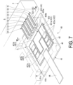
- connection conductor 5 may include a plurality of the pairs of the positive electrode-side busbar 51 and the negative electrode-side busbar 52.
- the plurality of pairs of the positive electrode-side busbar 51 and the negative electrode-side busbar 52 are arranged side by side at equal intervals in the direction in which the first opposing surface 510b and the second opposing surface 520b are opposed to each other.
- the pair of the positive electrode-side busbar 51 and the negative electrode-side busbar 52 are arranged side by side with a gap G therebetween, and the insulation distance is secured between the pair of the positive electrode-side busbar 51 and the negative electrode-side busbar 52.
- each positive electrode-side busbar 51 is connected to the first front surface pattern 421a through the P-type terminal 431 (indicated by a solid line), and each negative electrode-side busbar 52 is connected to the second front surface pattern 421b through the N-type terminal 432 (indicated by a solid line).
- connection conductor 5 is constituted by the plurality of pairs of the positive electrode-side busbar 51 and the negative electrode-side busbar 52.
- the current path is divided into a plurality of paths, and the total opposing areas of the first opposing surface 510b and the second opposing surface 520b in the positive electrode-side busbar 51 and the negative electrode-side busbar 52 can be increased.
- the parasitic inductance generated in the connection conductor 5 can be further reduced.
- FIGS. 7 and 8 illustrate a case where the first main body portion 510 of the positive electrode-side busbar 51 and the second main body portion 520 of the negative electrode-side busbar 52 each have the triangular prism shape, but a configuration is not limited to this configuration.
- the positive electrode-side busbar 51 and the negative electrode-side busbar 52 may have the configurations described in modifications 1 to 3.
- the first bottom surface 510a of the first main body portion 510 is integrally connected to the P-type terminal 431 and the second bottom surface 520a of the second main body portion 520 is connected to the N-type terminal 432 by welding.
- a configuration is not limited to this configuration.
- the first main body portion 510 and the P-type terminal 431, and the second main body portion 520 and the N-type terminal 432 may be connected to each other by a fastening member or the like including a bolt and a nut.
- the first cutout portion 511 may be disposed in a portion of the first main body portion 510.
- the second cutout 521 may also be disposed in a portion of the second main body portion 520.
- the configurations of the first main body portion 510 and the second main body portion 520 are not limited to the above, and for example, in the first main body portion 510 and the second main body portion 520, only a portion where the fastening member is disposed and connected to the main terminal portion 43 may be formed in a flat plate shape.
- first cutout portion 511 may be disposed in at least part of the first main body portion 510 on a side opposite to the first bottom surface 510a and the first opposing surface 510b
- second cutout portion 521 may be disposed in at least part of the second main body portion 520 on a side opposite to the second bottom surface 520a and the second opposing surface 520b.
- the configuration in which the first surface 420a and the second surface 420b of the base plate 41 are respectively parallel to the first surface 420a and the second surface 420b of the insulating plate 420 in the back-to-back relationship has been described.
- a configuration is not limited to this configuration and may have a slightly inclined configuration.
- the configuration of the power conversion device 100 in which the power conversion unit 4 is a six-in-one module including three power modules 40 has been described.
- a configuration is not limited thereto.
- the power conversion unit 4 may be a two-in-one module including one power module 40.
- the inverter has been described as an example of the power conversion device 100.
- the power conversion device 100 is not limited to the inverter.
- the power conversion device 100 may be a device that performs power conversion by the power semiconductor element 422, such as a converter or a combination of an inverter and a converter.
- an AC voltage may be input from an external input power supply (not illustrated) to the external output conductor 44, the power semiconductor element 422 on the circuit board 42 may convert the AC voltage into a DC voltage, and the DC voltage from the power semiconductor element 422 may be output to the outside of the power conversion device 100 through the main terminal portion 43 and the connection conductor 5.
- the power conversion device described in the embodiment is understood as follows, for example.
- the power conversion device 100 according to a second aspect is the power conversion device 100 according to the first aspect, wherein a dimension of the first opposing surface 510b in a direction perpendicular to the first bottom surface 510a is H, a dimension of the first bottom surface 510a in a direction in which the first opposing surface 510b and the second opposing surface 520b are opposed is W, and 0.2 ⁇ H/W ⁇ 1 may be satisfied.
- the power conversion device 100 according to a third aspect is the power conversion device 100 according to the first aspect or the second aspect, in which the connection conductor 5 may include a plurality of pairs of the positive electrode-side busbar 51 and the negative electrode-side busbar 52.
- the plurality of pairs of the positive electrode-side busbar 51 and the negative electrode-side busbar 52 may be arranged side by side at equal intervals in a direction in which the first opposing surface 510b and the second opposing surface 520b are opposed to each other.
- the current path is divided into a plurality of paths, and the total opposing areas of the first opposing surface 510b and the second opposing surface 520b in the positive electrode-side busbar 51 and the negative electrode-side busbar 52 can be increased.
- a power conversion device that can reduce parasitic inductance generated in a connection conductor while suppressing an increase in size and weight of the connection conductor can be provided.
Landscapes
- Engineering & Computer Science (AREA)
- Power Engineering (AREA)
- Microelectronics & Electronic Packaging (AREA)
- Manufacturing & Machinery (AREA)
- Inverter Devices (AREA)
Abstract
Description
- The present disclosure relates to a power conversion device.
- Priority is claimed by the present application on
JP 2022-75380, filed Apr. 28, 2022 - For example, Patent Document 1 discloses a power conversion device in which a positive electrode side conductor and a negative electrode side conductor each connected to a capacitor are stacked in a laminate structure sandwiching an insulating layer therebetween.
- The positive electrode side conductor and the negative electrode side conductor as connection conductors both have a flat plate shape and are opposed in a state of being parallel to each other with the insulating layer therebetween.
- Accordingly, when a current flows through the positive electrode side conductor and the negative electrode side conductor, magnetic fluxes generated in the positive electrode side conductor and the negative electrode side conductor cancel each other, and as a result, parasitic inductance is reduced.
- For example,
Patent Document 2 discloses a semiconductor device including a main terminal group as a connection conductor configured by continuously arranging three or more main terminals. - In the main terminal group, a main terminal as a collector terminal connected to a collector electrode of a semiconductor chip and a main terminal as an emitter terminal connected to an emitter electrode of the semiconductor chip are alternately arranged in a state of being adjacent to each other.
- That is, side surface facing portions of the main terminals are arranged in parallel.
- Accordingly, since the side surfaces of the plurality of collector terminals and the emitter terminals are opposed to each other, when a main current flows through the collector terminals and the emitter terminals, magnetic fluxes generated in the collector terminals and the emitter terminals cancel each other, and as a result, the parasitic inductance is reduced.
-
- Patent Document 1:
JP2002-119069 A - Patent Document 2:
WO 2020/021881 A - In recent years, in the field of a power conversion device including a power semiconductor element, there has been an increasing trend toward higher voltage, larger current, higher frequency, and faster switching in order to improve added value.
- Accordingly, it is desired to further reduce parasitic inductance generated in a connection conductor.
- In the laminate structure in the power conversion device described in Patent Document 1, there is a high risk of dielectric breakdown occurring in the insulating layer sandwiched between the positive electrode side conductor and the negative electrode side conductor.
- When the thickness of the insulating layer is increased for the purpose of avoiding the dielectric breakdown of the insulating layer, an interaction that cancels the magnetic fluxes between the positive electrode side conductor and the negative electrode side conductor each other may be reduced.
- In the semiconductor device described in
Patent Document 2, among the surfaces of the main terminals, the side surfaces each having a relatively small area are opposed to each other. - Therefore, for example, as compared with the arrangement of the positive electrode side conductor and the negative electrode side conductor described in Patent Document 1, the magnetic fluxes generated in the main terminals may not smoothly cancel each other.
- For example, in a case where the main terminal is formed or disposed to be thick so that the area of the opposing surface is increased, the main terminal may be increased in size and weight.
- The present disclosure has been made to solve the above problem, and an object of the present disclosure is to provide a power conversion device that can reduce parasitic inductance generated in a connection conductor while suppressing an increase in size and weight of the connection conductor.
- In order to solve the above problem, a power conversion device according to the present disclosure includes a capacitor to which DC power is supplied, a power module configured to convert a DC voltage from the capacitor into an AC voltage and output the AC voltage, and a connection conductor including a positive electrode-side busbar configured to connect the capacitor and a P-type terminal of the power module and a negative electrode-side busbar having a shape identical to a shape of the positive electrode-side busbar, symmetrically arranged side by side with the positive electrode-side busbar in pairs with a gap therebetween, and configured to connect the capacitor and an N-type terminal of the power module. The positive electrode-side busbar includes a first main body portion including a first bottom surface abutting on the P-type terminal and a first opposing surface rising from the first bottom surface and a first cutout portion disposed in at least part of the first main body portion on a side opposite to the first bottom surface and the first opposing surface. The negative electrode-side busbar includes a second main body portion including a second bottom surface abutting on the N-type terminal and a second opposing surface rising from the second bottom surface and disposed in parallel to and opposed to the first opposing surface with a gap therebetween and a second cutout portion disposed in part of the second main body portion on a side opposite to the second bottom surface and the second opposing surface.
- According to the present disclosure, a power conversion device that can reduce parasitic inductance generated in a connection conductor while suppressing an increase in size and weight of the connection conductor can be provided.
-
-
FIG. 1 is a perspective view illustrating a schematic configuration of a power conversion device according to an embodiment of the present disclosure. -
FIG. 2 is an enlarged perspective view of a main part of the power conversion device illustrated inFIG. 1 . -
FIG. 3 is a cross-sectional view taken along line III-III illustrated inFIG. 2 . -
FIG. 4 is a cross-sectional view of a connection conductor according to another embodiment of the present disclosure, corresponding to the portion illustrated inFIG. 3 . -
FIG. 5 is a cross-sectional view of a connection conductor according to another embodiment of the present disclosure, corresponding to the portion illustrated inFIG. 3 . -
FIG. 6 is a cross-sectional view of a connection conductor according to another embodiment of the present disclosure, corresponding to the portion illustrated inFIG. 3 . -
FIG. 7 is an enlarged perspective view illustrating a main part of the power conversion device according to another embodiment of the present disclosure. -
FIG. 8 is a cross-sectional view taken along line VIII-VIII illustrated inFIG. 7 . - Hereinafter, embodiments for implementing a power conversion device according to the present disclosure will be described with reference to the accompanying drawings.
- The power conversion device is a device that converts DC power into AC power, converts AC power into DC power, or converts DC power into DC power having a different potential.
- Examples of the power conversion device of the present embodiment include an inverter used in a system of a power plant or the like, an inverter used for driving an electric motor of an electric vehicle, or the like.
- In the present embodiment, an inverter for controlling an electric motor (motor) will be described as an example of the power conversion device.
- As illustrated in
FIG. 1 , apower conversion device 100 includes a casing 1, anexternal input conductor 2, acapacitor 3, apower conversion unit 4, acooling device 6, and aconnection conductor 5. - The casing 1 forms an outer shell of the
power conversion device 100. - The casing 1 in the present embodiment is made of a metal such as aluminum, a synthetic resin, or the like, and has a rectangular parallelepiped shape.
- The casing 1 includes two side surfaces arranged so as to be back-to-back with each other.
- Hereinafter, among these two side surfaces, a side surface opposing one side is referred to as an "input-
side side surface 1a", and a side surface opposing the other side is referred to as an "output-side side surface 1b". - The
external input conductor 2 for inputting DC power is led out from the input-side side surface 1a. - The
external input conductors 2 are a pair of electrical conductors (busbars) that supply DC power supplied from a DC power supply or the like provided outside thepower conversion device 100 to thecapacitor 3. - The
external input conductor 2 in the present embodiment is made of a metal including copper or the like. - One end of the
external input conductor 2 is connected to thecapacitor 3, and the other end of theexternal input conductor 2 extends in a direction intersecting the input-side side surface 1a of the casing 1. - The
capacitor 3 is a smoothing capacitor for storing electric charge input from theexternal input conductor 2 and suppressing voltage fluctuation associated with power conversion. - The DC voltage smoothed by suppressing ripples through the
capacitor 3 is supplied to thepower conversion unit 4. - The
power conversion unit 4 converts the voltage input from thecapacitor 3. - In order to output three-phase AC power, the
power conversion unit 4 in the present embodiment includes threepower modules 40 responsible for outputs for the U phase, the V phase, and the W phase, respectively. - The
power module 40 is a device that converts input power and outputs the converted power. - The
power module 40 in the present embodiment constitutes a part of thepower conversion unit 4. - As illustrated in
FIG. 2 , thepower module 40 includes abase plate 41, acircuit board 42, amain terminal portion 43, anexternal output conductor 44, and a reinforcingportion 45. - The
base plate 41 is a member having a flat plate shape. - The
base plate 41 includes amain surface 41a and aback surface 41b located on the back side of themain surface 41a. - That is, the
main surface 41a and theback surface 41b of thebase plate 41 are back-to-back in a state of being parallel to each other. - The
back surface 41b of thebase plate 41 is fixed to, for example, thecooling device 6 with a bonding material or the like (not illustrated) therebetween. - The
base plate 41 in the present embodiment is made of, for example, copper. - The
base plate 41 may be made of a metal other than copper. - The
circuit board 42 includes an insulatingplate 420, afront surface pattern 421, apower semiconductor element 422, and a back surface pattern (not illustrated for convenience of illustration). - The insulating
plate 420 has a flat plate shape. - The insulating
plate 420 includes afirst surface 420a and asecond surface 420b located on the back side of thefirst surface 420a. - That is, the
first surface 420a and thesecond surface 420b of the insulatingplate 420 are back-to-back in a state of being parallel to each other. - A back surface pattern, which is a pattern of copper foil or the like, is formed on the
second surface 420b of the insulatingplate 420. - The back surface pattern is fixed to the center of the
main surface 41a of thebase plate 41 with a bonding material or the like (not illustrated) therebetween. - The insulating
plate 420 is made of an insulating material such as ceramic. - In addition to ceramic, paper phenol, paper epoxy, glass composite, glass epoxy, glass polyimide, fluororesin, or the like can be used as the insulating material forming the insulating
plate 420. - The
front surface pattern 421 is a pattern of copper foil or the like formed on thefirst surface 420a of the insulatingplate 420 and extending in a planar shape. - The
front surface pattern 421 is formed by, for example, being fixed to thefirst surface 420a of the insulatingplate 420 by adhesion or the like and then being etched or the like. - A plurality of the
front surface patterns 421 are disposed on thefirst surface 420a of the insulatingplate 420. - The plurality of
front surface patterns 421 are arranged adjacent to each other with a gap therebetween in a direction in which the insulatingplate 420 extends. - In the present embodiment, a case where three
front surface patterns 421 are arranged on thefirst surface 420a will be described as an example. - Hereinafter, for convenience of description, these three
front surface patterns 421 are referred to as a firstfront surface pattern 421a, a secondfront surface pattern 421b, and a thirdfront surface pattern 421c. - The main terminal portion 43 (P-type terminal 431) as a positive electrode for inputting a direct current is connected to the first
front surface pattern 421a. - The main terminal portion 43 (N-type terminal 432) as a negative electrode for outputting a direct current is connected to the second
front surface pattern 421b. - That is, the first
front surface pattern 421a corresponds to an inlet portion of a loop between P and N formed in thefront surface pattern 421, and the secondfront surface pattern 421b corresponds to an outlet portion of the loop between P and N. - The
external output conductor 44 for outputting an alternating current converted by thepower semiconductor element 422 to a load such as a motor (not illustrated) provided outside thepower conversion device 100 is connected to the thirdfront surface pattern 421c. - The
power semiconductor element 422 is a circuit element that converts power by a switching operation of turning on and off a voltage or a current. - The
power semiconductor element 422 is, for example, a switching element such as an IGBT or a MOSFET. - In the present embodiment, as an example, six
power semiconductor elements 422 are connected to thefront surface pattern 421 on thecircuit board 42. - The six
power semiconductor elements 422 in the present embodiment include three firstpower semiconductor elements 422a and three secondpower semiconductor elements 422b. - The first
power semiconductor element 422a is connected to the firstfront surface pattern 421a. - The second
power semiconductor element 422b is connected to the thirdfront surface pattern 421c. - When the
power semiconductor element 422 is the IGBT, thepower semiconductor element 422 includes an input surface on which an input terminal corresponding to a collector is formed, an output surface on which an output terminal corresponding to an emitter is formed, and a gate corresponding to a control signal input terminal for controlling switching of thepower semiconductor element 422. - The input surface of the
power semiconductor element 422 is electrically connected to thefront surface pattern 421 with a bonding material or the like (not illustrated) therebetween. - For example, one end of a bonding wire (not illustrated) as a conducting wire is electrically connected to the output surface of the
power semiconductor element 422. - The input surface of the first
power semiconductor element 422a is connected to the firstfront surface pattern 421a. - The other end of the bonding wire connected to the output surface of the first
power semiconductor element 422a is connected to the thirdfront surface pattern 421c. - The input surface of the second
power semiconductor element 422b is connected to the thirdfront surface pattern 421c. - The other end of the bonding wire connected to the output surface of the second
power semiconductor element 422b is connected to the secondfront surface pattern 421b. - DC power is input to the input terminal of the first
power semiconductor element 422a through the firstfront surface pattern 421a, and the input DC power is converted into AC power by the firstpower semiconductor element 422a. - The converted AC power is output from an output terminal (not illustrated) in the first
power semiconductor element 422a to the thirdfront surface pattern 421c through a bonding wire. - AC power is input to the input terminal of the second
power semiconductor element 422b through the thirdfront surface pattern 421c, and the input AC power is converted into DC power by the secondpower semiconductor element 422b. - The converted DC power is output from an output terminal (not illustrated) in the second
power semiconductor element 422b to the secondfront surface pattern 421b through a bonding wire. - A control signal generated by a control unit (not illustrated) provided outside the
circuit board 42 is input to thepower semiconductor element 422. - The
power semiconductor element 422 performs switching in accordance with the control signal. - When the
power semiconductor element 422 is the MOSFET, thepower semiconductor element 422 includes an input surface corresponding to a drain, an output surface corresponding to a source, and a gate corresponding to a control signal input terminal. - For example, solder, a sintered material (powder of a metal or the like), or the like can be adopted as the above-described bonding material used for bonding the
base plate 41 and the back surface pattern formed on thesecond surface 420b of the insulatingplate 420 to each other, bonding thepower semiconductor element 422 and thefront surface pattern 421 to each other, and bonding theback surface 41b of thebase plate 41 and thecooling device 6 to each other. - The main
terminal portion 43 is an electric conductor (busbar) that exchanges DC power between thecapacitor 3 and thecircuit board 42. - The main
terminal portion 43 is made of a metal such as copper. - The main
terminal portion 43 includes the P-type terminal 431 as the positive electrode and the N-type terminal 432 as the negative electrode. - The P-
type terminal 431 and the N-type terminal 432 are arranged side by side with a gap therebetween. - In other words, the N-
type terminal 432 is arranged side by side with the P-type terminal 431 with a gap therebetween. - The P-
type terminal 431 and the N-type terminal 432 have the same size and shape. - The term "same" in the present embodiment refers to a substantially same state, and a slight manufacturing error and a design tolerance are allowed.
- The P-
type terminal 431 includes oneend portion 431b connected to the firstfront surface pattern 421a, and theother end portion 431a which extends integrally with the oneend portion 431b from the oneend portion 431b and into which a direct current from the positive electrode of thecapacitor 3 flows. - The
other end portion 431a of the P-type terminal 431 has a flat plate shape. - The N-
type terminal 432 includes oneend portion 432b connected to the secondfront surface pattern 421b and theother end portion 432a extending integrally with the oneend portion 432b from the oneend portion 432b and allowing a direct current to flow out toward the negative electrode of thecapacitor 3. - The
other end portion 432a of the N-type terminal 432 has a flat plate shape. - The
external output conductor 44 is an electrical conductor (busbar) for outputting the AC power converted by thepower semiconductor element 422 to the outside of thepower conversion device 100. - The
external output conductor 44 is made of a metal including copper or the like. - One end of the
external output conductor 44 is connected to the thirdfront surface pattern 421c on thecircuit board 42. - As illustrated in
FIG. 1 , the other end of theexternal output conductor 44 extends outward beyond the output-side side surface 1b of the casing 1. - A wiring (not illustrated) for current output connected to a load such as a motor is connected to the other end of the
external output conductor 44, for example. - As indicated by a two-dot chain line in
FIG. 2 , the reinforcingportion 45 is a member that is fixed to themain surface 41a of thebase plate 41 and mechanically reinforces the mainterminal portion 43 and theexternal output conductor 44. - The reinforcing
portion 45 is made of a synthetic resin material or the like. - The reinforcing
portion 45 covers the mainterminal portion 43 and theexternal output conductor 44 from the outside and surrounds thecircuit board 42 from the outside. - The reinforcing
portion 45 forms a case surrounding thecircuit board 42 from the periphery in a direction along themain surface 41a of thebase plate 41. - Therefore, the reinforcing
portion 45 defines a space in which thecircuit board 42 is accommodated together with thebase plate 41. - The reinforcing
portion 45 is fixed to thefirst surface 420a of thebase plate 41 with an adhesive or the like therebetween. - For example, an insulating material such as polyphenylene sulfide (PPS) can be adopted as the synthetic resin material for the reinforcing
portion 45 in the present embodiment. - An insulating material other than PPS may be used for the reinforcing
portion 45. - Hereinafter, in the present embodiment, the space defined by the reinforcing
portion 45 and thebase plate 41 is referred to as a potting space P. - A liquid potting material (not illustrated) is poured (potting) into the potting space P from the outside, and the
front surface pattern 421 on thecircuit board 42 and thepower semiconductor element 422 each exposed to the potting space P are sealed. - The potting material poured into the potting space P is cured over a predetermined time, and electrically insulates the
front surface pattern 421 on thecircuit board 42 and thepower semiconductor element 422 from a space outside thepower module 40. - As the potting material in the present embodiment, for example, silicone gel, an epoxy resin, or the like is adopted.
- A synthetic resin other than the silicone gel and the epoxy resin may be used as the potting material.
- As illustrated in
FIG. 1 , thecooling device 6 is a device that mainly cools thepower module 40 of thepower conversion unit 4. - The
cooling device 6 is provided so as to be stacked on the casing 1, and is fixed to and integrated with the casing 1. - A liquid refrigerant such as water is introduced into the
cooling device 6 from the outside. - The liquid refrigerant exchanges heat with the
power module 40 and is heated, thereby cooling thepower module 40. - Hereinafter, the configuration of the
connection conductor 5 that relays DC power between thecapacitor 3 and thepower module 40 will be described with reference toFIGS. 2 and3 . - The
connection conductor 5 is an electrical conductor (busbar) made of a metal including copper or the like. - In the present embodiment, three
connection conductors 5 are arranged at intervals so as to correspond to thepower modules 40. respectively. - Each
connection conductor 5 includes a positive electrode-side busbar 51 and a negative electrode-side busbar 52. - The positive electrode-
side busbar 51 is a current path that connects the positive electrode of thecapacitor 3 and thepower module 40. - The negative electrode-
side busbar 52 is a current path that connects the negative electrode of thecapacitor 3 and thepower module 40. - The positive electrode-
side busbar 51 and the negative electrode-side busbar 52 are arranged side by side at an interval. - One end of each of the positive electrode-
side busbar 51 and the negative electrode-side busbar 52 is connected to thecapacitor 3. - A detailed illustration of connection states between the positive electrode-
side busbar 51 and thecapacitor 3 and between the negative electrode-side busbar 52 and thecapacitor 3 are omitted. - The other end of the positive electrode-
side busbar 51 is connected to the P-type terminal 431 in thepower module 40. - The other end of the negative electrode-
side busbar 52 is connected to the N-type terminal 432 of thepower module 40. - The positive electrode-
side busbar 51 and the negative electrode-side busbar 52 have the same size and shape. - The positive electrode-
side busbar 51 and the negative electrode-side busbar 52 in the present embodiment are symmetrically arranged side by side to form a pair. - Hereinafter, an interval generated between the positive electrode-
side busbar 51 and the negative electrode-side busbar 52 by being arranged side by side is referred to as a "gap G". - In other words, the negative electrode-
side busbar 52 is arranged side by side with the positive electrode-side busbar 51 with the gap G therebetween. - The gap G in the present embodiment has the same dimension as a gap G formed between the P-
type terminal 431 and the N-type terminal 432. - An insulation distance (a spatial distance and a creepage distance) is secured in the gap G so that a current flowing through the positive electrode-
side busbar 51 does not flow to the negative electrode-side busbar 52 or a current flowing through the negative electrode-side busbar 52 does not flow to the positive electrode-side busbar 51. - The insulation distance in the present embodiment is desirably, for example, 1 mm or more and 10 mm or less.
- As illustrated in
FIG. 3 , the positive electrode-side busbar 51 includes a firstmain body portion 510 and afirst cutout portion 511. - The first
main body portion 510 in the present embodiment has a columnar shape extending in one direction between thecapacitor 3 and thepower module 40. - The first
main body portion 510 includes afirst bottom surface 510a abutting on the P-type terminal 431 and a first opposingsurface 510b rising from thefirst bottom surface 510a. - In the present embodiment, the
first bottom surface 510a and the first opposingsurface 510b are perpendicular to each other. - The term "perpendicular" in the present embodiment refers to a substantially perpendicular state, and a slight manufacturing error and a design tolerance are allowed.
- The
first bottom surface 510a is integrally connected to the P-type terminal 431 by, for example, welding. - The
first cutout portion 511 is disposed in the firstmain body portion 510 on a side opposite to thefirst bottom surface 510a and the first opposingsurface 510b. - Here, the
first cutout portion 511 is disposed so as to cut out, in a triangular prism shape in the direction in which the base material X extends, one corner disposed on a side opposite to thefirst bottom surface 510a forming a bottom surface of a base material X and the first opposingsurface 510b forming a side surface of the base material X among four corners of the base material X forming a quadrangular prism shape forming the firstmain body portion 510. - A first
inclined surface 510c that connects an end edge of thefirst bottom surface 510a and an end edge of the first opposingsurface 510b to each other is formed in the firstmain body portion 510 by thefirst cutout portion 511. - Therefore, in the present embodiment, the first
main body portion 510 is formed in a triangular prism shape having a right-angled triangular cross section by thefirst bottom surface 510a, the first opposingsurface 510b, and the firstinclined surface 510c included in the firstmain body portion 510. - The "cross section" in the present embodiment means a plane obtained by cutting the first
main body portion 510 along a plane orthogonal to the direction in which the firstmain body portion 510 extends. - The negative electrode-
side busbar 52 includes a secondmain body portion 520 and asecond cutout portion 521. - The second
main body portion 520 in the present embodiment has a columnar shape extending in the same direction as the direction in which the firstmain body portion 510 extends between thecapacitor 3 and thepower module 40. - The second
main body portion 520 includes asecond bottom surface 520a abutting on the N-type terminal 432 and a second opposingsurface 520b rising from thesecond bottom surface 520a. - In the present embodiment, the
second bottom surface 520a and the first opposingsurface 510b are perpendicular to each other. - The
second bottom surface 520a is integrally connected to the P-type terminal 431 by, for example, welding. - The second opposing
surface 520b is disposed in parallel to and opposed to the first opposingsurface 510b with the gap G therebetween. - The
second cutout portion 521 is disposed in the secondmain body portion 520 on a side opposite to thesecond bottom surface 520a and the second opposingsurface 520b. - Here, the
second cutout portion 521 is disposed so as to cut out, in a triangular prism shape in the direction in which the base material X extends, one corner disposed on a side opposite to thesecond bottom surface 520a forming a bottom surface of a base material X and the second opposingsurface 520b forming a side surface of the base material X among four corners of the base material X forming a quadrangular prism shape forming the secondmain body portion 520. - A second
inclined surface 520c that connects an end edge of thesecond bottom surface 520a and an end edge of the second opposingsurface 520b to each other is formed in the secondmain body portion 520 by thesecond cutout portion 521. - Therefore, in the present embodiment, the second
main body portion 520 is formed in a triangular prism shape having a right-angled triangular cross section by thesecond bottom surface 520a, the second opposingsurface 520b, and the secondinclined surface 520c included in the secondmain body portion 520. - Here, a dimension of the first opposing
surface 510b and the second opposingsurface 520b in the direction perpendicular to thefirst bottom surface 510a and thesecond bottom surface 520a, respectively, is H, a dimension of thefirst bottom surface 510a and thesecond bottom surface 520a in the direction in which the first opposingsurface 510b and the second opposingsurface 520b are opposed is W, and the following expression (i) is established.
- A current input from the
capacitor 3 to thefront surface pattern 421 through the positive electrode-side busbar 51 and the P-type terminal 431 each as the positive electrode is converted by thepower semiconductor element 422 and then used for rotation of a motor or the like (load) provided outside thepower conversion device 100 through theexternal output conductor 44. - The current used for the rotation of the motor or the like flows into the
front surface pattern 421 again through theexternal output conductor 44, is converted by thepower semiconductor element 422, and then returns to thecapacitor 3 through the N-type terminal 432 and the negative electrode-side busbar 52 each as the negative electrode. - At this time, the positive electrode-
side busbar 51 and the negative electrode-side busbar 52 are arranged side by side with the gap G therebetween, and a flow direction of the current flowing through the positive electrode-side busbar 51 and a flow direction of the current flowing through the negative electrode-side busbar 52 are opposite to each other. - This causes a magnetic flux generated in the positive electrode-
side busbar 51 and a magnetic flux generated in the negative electrode-side busbar 52 to be canceled each other. - Since the magnitude of the current flowing in the
front surface pattern 421 is rapidly changed by the switching of thepower semiconductor element 422 on thecircuit board 42, densities of the magnetic fluxes generated in the positive electrode-side busbar 51 and the negative electrode-side busbar 52 are rapidly changed according to the change. - At this time, in the positive electrode-
side busbar 51 and the negative electrode-side busbar 52, counter electromotive forces (eddy currents) that generate magnetic fluxes that cancel changes in the densities of the magnetic fluxes are also generated. - The above-described configuration can secure larger areas of the first opposing
surface 510b of the firstmain body portion 510 and the second opposingsurface 520b of the secondmain body portion 520 by thefirst cutout portion 511 disposed in the firstmain body portion 510 and thesecond cutout portion 521 disposed in the secondmain body portion 520 as compared with, for example, aconnection conductor 5 having a flat plate shape (quadrangular prism). - That is, opposing areas of the first
main body portion 510 and the secondmain body portion 520 can be increased. - This can increase amounts of magnetic fluxes that cancel each other between the positive electrode-
side busbar 51 and the negative electrode-side busbar 52. - It is possible to secure large areas of the first opposing
surface 510b of the firstmain body portion 510 and the second opposingsurface 520b of the secondmain body portion 520 without changing cross-sectional areas and weights of the firstmain body portion 510 and the secondmain body portion 520. - Thus parasitic inductance generated in the
connection conductor 5 can be reduced while suppressing an increase in size and weight of theconnection conductor 5. - Although the embodiments of the present disclosure have been described above in detail with reference to the drawings, specific configurations are not limited to the configurations of the embodiments, and additions, omissions, substitutions, and other modifications of the configurations can be made without departing from the gist of the present disclosure.
- In the above embodiment, the configuration of the first
main body portion 510 and the secondmain body portion 520 formed in the triangular prism shape having the right-angled triangular cross section has been described. However, a configuration is not limited to this configuration. - Hereinafter, shapes that the first
main body portion 510 and the secondmain body portion 520 can have will be described in a plurality of modifications (modifications 1 to 3). - In the configuration described below, the above equation (i) is satisfied.
- The positive electrode-
side busbar 51 and the negative electrode-side busbar 52 may have configurations as illustrated inFIG. 4 , for example. - In this case, the positive electrode-
side busbar 51 includes the firstmain body portion 510 and thefirst cutout portion 511. - The first
main body portion 510 includes thefirst bottom surface 510a abutting on the P-type terminal 431, the first opposingsurface 510b rising from thefirst bottom surface 510a, and afirst side surface 510d rising from thefirst bottom surface 510a and opposing a side opposite to the first opposingsurface 510b in a state of being parallel to the first opposingsurface 510b. - The
first cutout portion 511 is disposed in the firstmain body portion 510 on a side opposite to thefirst bottom surface 510a and the first opposingsurface 510b. - The
first cutout portion 511 is disposed so as to cut out, in a triangular prism shape in the direction in which the base material X extends, one corner disposed on a side opposite to thefirst bottom surface 510a forming a bottom surface of a base material X and the first opposingsurface 510b forming a side surface of the base material X among four corners of the base material X forming a quadrangular prism shape forming the firstmain body portion 510. - A first
inclined surface 510c that connects an end edge of the first opposingsurface 510b and an end edge of thefirst side surface 510d to each other is formed in the firstmain body portion 510 by thefirst cutout portion 511. - Therefore, the first
main body portion 510 in this configuration is formed in a quadrangular prism shape having a trapezoidal cross section by thefirst bottom surface 510a, the first opposingsurface 510b, thefirst side surface 510d, and the firstinclined surface 510c included in the firstmain body portion 510. - Therefore, when viewing the cross section of the first
main body portion 510, thefirst side surface 510d corresponds to an upper base of the trapezoidal shape, and the first opposingsurface 510b corresponds to a lower base of the trapezoidal shape. - The negative electrode-
side busbar 52 includes a secondmain body portion 520 and asecond cutout portion 521. - The second
main body portion 520 includes thesecond bottom surface 520a abutting on the N-type terminal 432, the second opposingsurface 520b rising from thesecond bottom surface 520a, and asecond side surface 520d rising from thesecond bottom surface 520a and opposing a side opposite to the second opposingsurface 520b in a state of being parallel to the second opposingsurface 520b. - The second opposing
surface 520b is disposed in parallel to and opposed to the first opposingsurface 510b with the gap G therebetween. - The
second cutout portion 521 is disposed in the secondmain body portion 520 on a side opposite to thesecond bottom surface 520a and the second opposingsurface 520b. - The
second cutout portion 521 is disposed so as to cut out, in a triangular prism shape in the direction in which the base material X extends, one corner disposed on a side opposite to thesecond bottom surface 520a forming a bottom surface of a base material X and the second opposingsurface 520b forming a side surface of the base material X among four corners of the base material X forming a quadrangular prism shape forming the secondmain body portion 520. - A second
inclined surface 520c that connects an end edge of the second opposingsurface 520b and an end edge of thesecond side surface 520d to each other is formed in the secondmain body portion 520 by thesecond cutout portion 521. - Therefore, the second
main body portion 520 in this configuration is formed in a quadrangular prism shape having a trapezoidal cross section by thesecond bottom surface 520a, the second opposingsurface 520b, thesecond side surface 520d, and the secondinclined surface 520c included in the secondmain body portion 520. - Therefore, when viewing the cross section of the second
main body portion 520, thesecond side surface 520d corresponds to an upper base of the trapezoidal shape, and the second opposingsurface 520b corresponds to a lower base of the trapezoidal shape. - The positive electrode-
side busbar 51 and the negative electrode-side busbar 52 may have configurations as illustrated inFIG. 5 , for example. - In this case, the positive electrode-
side busbar 51 includes the firstmain body portion 510 and thefirst cutout portion 511. - The first
main body portion 510 includes thefirst bottom surface 510a abutting on the P-type terminal 431, the first opposingsurface 510b rising from thefirst bottom surface 510a, thefirst side surface 510d rising from thefirst bottom surface 510a and opposing a side opposite to the first opposingsurface 510b in a state of being parallel to the first opposingsurface 510b, and a firstupper surface 510e that is connected to the first opposingsurface 510b and faces a side opposite to thefirst bottom surface 510a in a state of being parallel to thefirst bottom surface 510a. - The
first cutout portion 511 is disposed in the firstmain body portion 510 on a side opposite to thefirst bottom surface 510a and the first opposingsurface 510b. - The
first cutout portion 511 is disposed so as to cut out, in a triangular prism shape in the direction in which the base material X extends, one corner disposed on a side opposite to thefirst bottom surface 510a forming a bottom surface of a base material X and the first opposingsurface 510b forming a side surface of the base material X among four corners of the base material X forming a quadrangular prism shape forming the firstmain body portion 510. - A first
inclined surface 510c that connects an end edge of the firstupper surface 510e and an end edge of thefirst side surface 510d to each other is formed in the firstmain body portion 510 by thefirst cutout portion 511. - Therefore, the first
main body portion 510 in this configuration is formed in a pentagonal prism shape having a pentagonal cross section by thefirst bottom surface 510a, the first opposingsurface 510b, thefirst side surface 510d, theupper surface 510e, and the firstinclined surface 510c included in the firstmain body portion 510. - The negative electrode-
side busbar 52 includes a secondmain body portion 520 and asecond cutout portion 521. - The second
main body portion 520 includes thesecond bottom surface 520a abutting on the N-type terminal 432, the second opposingsurface 520b rising from thesecond bottom surface 520a, thesecond side surface 520d rising from thesecond bottom surface 520a and opposing a side opposite to the second opposingsurface 520b in a state of being parallel to the second opposingsurface 520b, and a secondupper surface 520e that is connected to the second opposingsurface 520b and faces a side opposite to thesecond bottom surface 520a in a state of being parallel to thesecond bottom surface 520a. - The second opposing
surface 520b is disposed in parallel to and opposed to the first opposingsurface 510b with the gap G therebetween. - The
second cutout portion 521 is disposed in the secondmain body portion 520 on a side opposite to thesecond bottom surface 520a and the second opposingsurface 520b. - The
second cutout portion 521 is disposed so as to cut out, in a triangular prism shape in the direction in which the base material X extends, one corner disposed on a side opposite to thesecond bottom surface 520a forming a bottom surface of a base material X and the second opposingsurface 520b forming a side surface of the base material X among four corners of the base material X forming a quadrangular prism shape forming the secondmain body portion 520. - A second
inclined surface 520c that connects an end edge of the secondupper surface 520e and an end edge of thesecond side surface 520d to each other is formed in the secondmain body portion 520 by thesecond cutout portion 521. - Therefore, the second
main body portion 520 in this configuration is formed in a pentagonal prism shape having a pentagonal cross section by thesecond bottom surface 520a, the second opposingsurface 520b, thesecond side surface 520d, the secondupper surface 520e, and the secondinclined surface 520c included in the secondmain body portion 520. - The positive electrode-
side busbar 51 and the negative electrode-side busbar 52 may have configurations as illustrated inFIG. 6 , for example. - In this case, the positive electrode-
side busbar 51 includes the firstmain body portion 510 and thefirst cutout portion 511. - The first
main body portion 510 includes thefirst bottom surface 510a abutting on the P-type terminal 431, the first opposingsurface 510b rising from thefirst bottom surface 510a, thefirst side surface 510d rising from thefirst bottom surface 510a and opposing a side opposite to the first opposingsurface 510b in a state of being parallel to the first opposingsurface 510b, and the firstupper surface 510e that is connected to the first opposingsurface 510b and faces a side opposite to thefirst bottom surface 510a in a state of being parallel to thefirst bottom surface 510a. - The
first cutout portion 511 is disposed in the firstmain body portion 510 on a side opposite to thefirst bottom surface 510a and the first opposingsurface 510b. - The
first cutout portion 511 is disposed so as to cut out, in a quadrangular prism shape in the direction in which the base material X extends, one corner disposed on a side opposite to thefirst bottom surface 510a forming a bottom surface of a base material X and the first opposingsurface 510b forming a side surface of the base material X among four corners of the base material X forming a quadrangular prism shape forming the firstmain body portion 510. - A
first cut surface 511a that connects an end edge of the firstupper surface 510e and an end edge of thefirst side surface 510d to each other is formed in the firstmain body portion 510 by thefirst cutout portion 511. - The
first cut surface 511a includes a firstopposite surface 510f that is connected to the firstupper surface 510e and faces a side opposite to the first opposingsurface 510b in a state of being parallel to the first opposingsurface 510b, and a firstfront surface 510g that connects the firstopposite surface 510f and thefirst side surface 510d to each other and faces a side opposite to thefirst bottom surface 510a in a state of being parallel to thefirst bottom surface 510a. - Therefore, the first
main body portion 510 in this configuration is formed in a hexagonal columnar shape having an L-shaped cross section by thefirst bottom surface 510a, the first opposingsurface 510b, thefirst side surface 510d, and thefirst cut surface 511a included in the firstmain body portion 510. - The negative electrode-
side busbar 52 includes a secondmain body portion 520 and asecond cutout portion 521. - The second
main body portion 520 includes thesecond bottom surface 520a abutting on the N-type terminal 432, the second opposingsurface 520b rising from thesecond bottom surface 520a, thesecond side surface 520d rising from thesecond bottom surface 520a and opposing a side opposite to the second opposingsurface 520b in a state of being parallel to the second opposingsurface 520b, and a secondupper surface 520e that is connected to the second opposingsurface 520b and faces a side opposite to thesecond bottom surface 520a in a state of being parallel to thesecond bottom surface 520a. - The second opposing
surface 520b is disposed in parallel to and opposed to the first opposingsurface 510b with the gap G there between. - The
second cutout portion 521 is disposed in the secondmain body portion 520 on a side opposite to thesecond bottom surface 520a and the second opposingsurface 520b. - The
second cutout portion 521 is disposed so as to cut out, in a quadrangular prism shape in the direction in which the base material X extends, one corner disposed on a side opposite to thesecond bottom surface 520a forming a bottom surface of a base material X and the second opposingsurface 520b forming a side surface of the base material X among four corners of the base material X forming a quadrangular prism shape forming the secondmain body portion 520. - A
second cut surface 521a that connects an end edge of the secondupper surface 520e and an end edge of thesecond side surface 520d to each other is formed in the secondmain body portion 520 by thesecond cutout portion 521. - The
second cut surface 521a includes a secondopposite surface 520f that is connected to the secondupper surface 520e and faces a side opposite to the second opposingsurface 520b in a state of being parallel to the second opposingsurface 520b, and a secondfront surface 520g that connects the secondopposite surface 520f and thesecond side surface 520d to each other and faces a side opposite to thesecond bottom surface 520a in a state of being parallel to thesecond bottom surface 520a. - Therefore, the second
main body portion 520 in this configuration is formed in a hexagonal columnar shape having an L-shaped cross section by thesecond bottom surface 520a, the second opposingsurface 520b, thesecond side surface 520d, and thesecond cut surface 521a included in the secondmain body portion 520. - A plurality of examples of the shapes that the first
main body portion 510 and the secondmain body portion 520 can have been described above. - Instead of the configuration of the
connection conductor 5 described above, as illustrated inFIG. 7 , theconnection conductor 5 may include a plurality of the pairs of the positive electrode-side busbar 51 and the negative electrode-side busbar 52. - In the present configuration, five pairs of the positive electrode-
side busbar 51 and the negative electrode-side busbar 52 are exemplified. - At this time, as illustrated in
FIG. 8 , the plurality of pairs of the positive electrode-side busbar 51 and the negative electrode-side busbar 52 are arranged side by side at equal intervals in the direction in which the first opposingsurface 510b and the second opposingsurface 520b are opposed to each other. - The pair of the positive electrode-
side busbar 51 and the negative electrode-side busbar 52 are arranged side by side with a gap G therebetween, and the insulation distance is secured between the pair of the positive electrode-side busbar 51 and the negative electrode-side busbar 52. - Although detailed illustration is omitted, as illustrated in
FIG. 7 , each positive electrode-side busbar 51 is connected to the firstfront surface pattern 421a through the P-type terminal 431 (indicated by a solid line), and each negative electrode-side busbar 52 is connected to the secondfront surface pattern 421b through the N-type terminal 432 (indicated by a solid line). - According to the above configuration, the
connection conductor 5 is constituted by the plurality of pairs of the positive electrode-side busbar 51 and the negative electrode-side busbar 52. - Accordingly, as compared with a case where the
connection conductor 5 is a pair of the positive electrode-side busbar 51 and the negative electrode-side busbar 52, the current path is divided into a plurality of paths, and the total opposing areas of the first opposingsurface 510b and the second opposingsurface 520b in the positive electrode-side busbar 51 and the negative electrode-side busbar 52 can be increased. - Thus, the parasitic inductance generated in the
connection conductor 5 can be further reduced. -
FIGS. 7 and8 illustrate a case where the firstmain body portion 510 of the positive electrode-side busbar 51 and the secondmain body portion 520 of the negative electrode-side busbar 52 each have the triangular prism shape, but a configuration is not limited to this configuration. - That is, the positive electrode-
side busbar 51 and the negative electrode-side busbar 52 may have the configurations described in modifications 1 to 3. - In the above embodiment, the
first bottom surface 510a of the firstmain body portion 510 is integrally connected to the P-type terminal 431 and thesecond bottom surface 520a of the secondmain body portion 520 is connected to the N-type terminal 432 by welding. However, a configuration is not limited to this configuration. - The first
main body portion 510 and the P-type terminal 431, and the secondmain body portion 520 and the N-type terminal 432 may be connected to each other by a fastening member or the like including a bolt and a nut. - The
first cutout portion 511 may be disposed in a portion of the firstmain body portion 510. - The
second cutout 521 may also be disposed in a portion of the secondmain body portion 520. - The configurations of the first
main body portion 510 and the secondmain body portion 520 are not limited to the above, and for example, in the firstmain body portion 510 and the secondmain body portion 520, only a portion where the fastening member is disposed and connected to the mainterminal portion 43 may be formed in a flat plate shape. - That is, the
first cutout portion 511 may be disposed in at least part of the firstmain body portion 510 on a side opposite to thefirst bottom surface 510a and the first opposingsurface 510b, and thesecond cutout portion 521 may be disposed in at least part of the secondmain body portion 520 on a side opposite to thesecond bottom surface 520a and the second opposingsurface 520b. - In the embodiment, the configuration in which the
first surface 420a and thesecond surface 420b of thebase plate 41 are respectively parallel to thefirst surface 420a and thesecond surface 420b of the insulatingplate 420 in the back-to-back relationship has been described. However, a configuration is not limited to this configuration and may have a slightly inclined configuration. - In the above embodiment, the configuration of the
power conversion device 100 in which thepower conversion unit 4 is a six-in-one module including threepower modules 40 has been described. However, a configuration is not limited thereto. - For example, in the
power conversion device 100, thepower conversion unit 4 may be a two-in-one module including onepower module 40. - In the above embodiment, the inverter has been described as an example of the
power conversion device 100. However, thepower conversion device 100 is not limited to the inverter. - The
power conversion device 100 may be a device that performs power conversion by thepower semiconductor element 422, such as a converter or a combination of an inverter and a converter. - When the
power conversion device 100 is the converter, an AC voltage may be input from an external input power supply (not illustrated) to theexternal output conductor 44, thepower semiconductor element 422 on thecircuit board 42 may convert the AC voltage into a DC voltage, and the DC voltage from thepower semiconductor element 422 may be output to the outside of thepower conversion device 100 through the mainterminal portion 43 and theconnection conductor 5. - The power conversion device described in the embodiment is understood as follows, for example.
- (1) A
power conversion device 100 according to a first aspect includes acapacitor 3 to which DC power is supplied, apower module 40 configured to convert a DC voltage from thecapacitor 3 into an AC voltage and output the AC voltage, and aconnection conductor 5 including a positive electrode-side busbar 51 configured to connect thecapacitor 3 and a P-type terminal 431 of thepower module 40, and a negative electrode-side busbar 52 having a shape identical to a shape of the positive electrode-side busbar 51, symmetrically arranged side by side with the positive electrode-side busbar 51 in pairs with a gap G therebetween, and configured to connect thecapacitor 3 and an N-type terminal 432 of thepower module 40. The positive electrode-side busbar 51 includes a firstmain body portion 510 including afirst bottom surface 510a abutting on the P-type terminal 431 and a first opposingsurface 510b rising from thefirst bottom surface 510a and afirst cutout portion 511 disposed in at least part of the firstmain body portion 510 on a side opposite to thefirst bottom surface 510a and the first opposingsurface 510b. The negative electrode-side busbar 52 includes a secondmain body portion 520 including asecond bottom surface 520a abutting on the N-type terminal 432 and a second opposingsurface 520b rising from thesecond bottom surface 520a and disposed in parallel to and opposed to the first opposingsurface 510b with the gap G therebetween and asecond cutout portion 521 disposed in at least part of the secondmain body portion 520 on a side opposite to thesecond bottom surface 520a and the second opposingsurface 520b. - This can increase opposing areas of the first
main body portion 510 and the secondmain body portion 520. - That is, it is possible to increase amounts of magnetic fluxes that cancel each other between the positive electrode-
side busbar 51 and the negative electrode-side busbar 52. - It is possible to secure large areas of the first opposing
surface 510b of the firstmain body portion 510 and the second opposingsurface 520b of the secondmain body portion 520 without changing cross-sectional areas and weights of the firstmain body portion 510 and the secondmain body portion 520. - (2) The
power conversion device 100 according to a second aspect is thepower conversion device 100 according to the first aspect, wherein a dimension of the first opposingsurface 510b in a direction perpendicular to thefirst bottom surface 510a is H, a dimension of thefirst bottom surface 510a in a direction in which the first opposingsurface 510b and the second opposingsurface 520b are opposed is W, and 0.2 ≤ H/W ≤ 1 may be satisfied. - This can achieve the above-described action with more specific setting values.
- (3) The
power conversion device 100 according to a third aspect is thepower conversion device 100 according to the first aspect or the second aspect, in which theconnection conductor 5 may include a plurality of pairs of the positive electrode-side busbar 51 and the negative electrode-side busbar 52. The plurality of pairs of the positive electrode-side busbar 51 and the negative electrode-side busbar 52 may be arranged side by side at equal intervals in a direction in which the first opposingsurface 510b and the second opposingsurface 520b are opposed to each other. - Accordingly, as compared with a case where the
connection conductor 5 is a pair of the positive electrode-side busbar 51 and the negative electrode-side busbar 52, the current path is divided into a plurality of paths, and the total opposing areas of the first opposingsurface 510b and the second opposingsurface 520b in the positive electrode-side busbar 51 and the negative electrode-side busbar 52 can be increased. - According to the present disclosure, a power conversion device that can reduce parasitic inductance generated in a connection conductor while suppressing an increase in size and weight of the connection conductor can be provided.
-
- 1 Casing
- 1a Input-side side surface
- 1b Output-side side surface
- 2 External Input Conductor
- 3 Capacitor
- 4 Power conversion unit
- 5. Connection conductor
- 6 Cooling device
- 40 Power module
- 41 Base plate
- 41a Main surface
- 41b Back surface
- 42 Circuit board
- 43 Main terminal portion
- 44 External output conductor
- 45 Reinforcing portion
- 51 Positive electrode-side busbar
- 52 Negative electrode-side busbar
- 100 Power conversion device
- 420 Insulating plate
- 420a First surface
- 420b Second surface
- 421 Front surface pattern
- 421a First front surface pattern
- 421b Second front surface pattern
- 421c Third front surface pattern
- 422 Power semiconductor element
- 422a First power semiconductor element
- 422b Second power semiconductor element
- 431 P-type terminal
- 431a, 432a Other end portion
- 431b, 432b One end portion
- 432 N-type terminal
- 510 First main body portion
- 510a First bottom surface
- 510b First opposing surface
- 510c First inclined surface
- 510d First side surface
- 510e First upper surface
- 510f First opposite surface
- 510g First front surface
- 511 First cutout portion
- 511a First cut surface
- 520 Second main body portion
- 520a Second bottom surface
- 520b Second opposing surface
- 520c Second inclined surface
- 520d Second side surface
- 520e Second upper surface
- 520f Second opposite surface
- 520d Second front surface
- 521 Second cutout portion
- 521a Second cut surface
- G Gap
- P Potting space
- X Base material
Claims (3)
- A power conversion device, comprising:a capacitor to which DC power is supplied;a power module configured to convert a DC voltage from the capacitor into an AC voltage and output the AC voltage; anda connection conductor including a positive electrode-side busbar configured to connect the capacitor and a P-type terminal of the power module and a negative electrode-side busbar having a shape identical to a shape of the positive electrode-side busbar, symmetrically arranged side by side with the positive electrode-side busbar in pairs with a gap therebetween, and configured to connect the capacitor and an N-type terminal of the power module, whereinthe positive electrode-side busbar includesa first main body portion including a first bottom surface abutting on the P-type terminal and a first opposing surface rising from the first bottom surface anda first cutout portion disposed in at least part of the first main body portion on a side opposite to the first bottom surface and the first opposing surface, andthe negative electrode-side busbar includesa second main body portion including a second bottom surface abutting on the N-type terminal and a second opposing surface rising from the second bottom surface and disposed in parallel to and opposed to the first opposing surface with a gap therebetween anda second cutout portion disposed in at least part of the second main body portion on a side opposite to the second bottom surface and the second opposing surface.
- The power conversion device according to claim 1, whereina dimension of the first opposing surface in a direction perpendicular to the first bottom surface is H,a dimension of the first bottom surface in a direction in which the first opposing surface and the second opposing surface are opposed to each other is W, and
 is satisfied.
 - The power conversion device according to claim 1 or 2, whereinthe connection conductor includes a plurality of pairs of the positive electrode-side busbar and the negative electrode-side busbar, andthe plurality of pairs of the positive electrode-side busbar and the negative electrode-side busbar are arranged side by side at equal intervals in a direction in which the first opposing surface and the second opposing surface are opposed to each other.
Applications Claiming Priority (2)
| Application Number | Priority Date | Filing Date | Title |
|---|---|---|---|
| JP2022075380A JP7788932B2 (en) | 2022-04-28 | 2022-04-28 | Power Conversion Device |
| PCT/JP2023/003986 WO2023210098A1 (en) | 2022-04-28 | 2023-02-07 | Power conversion device |
Publications (3)
| Publication Number | Publication Date |
|---|---|
| EP4498591A1 true EP4498591A1 (en) | 2025-01-29 |
| EP4498591A4 EP4498591A4 (en) | 2025-07-23 |
| EP4498591B1 EP4498591B1 (en) | 2026-04-29 |
Family
ID=88518336
Family Applications (1)
| Application Number | Title | Priority Date | Filing Date |
|---|---|---|---|
| EP23795846.7A Active EP4498591B1 (en) | 2022-04-28 | 2023-02-07 | Power conversion device |
Country Status (4)
| Country | Link |
|---|---|
| US (1) | US20250274052A1 (en) |
| EP (1) | EP4498591B1 (en) |
| JP (1) | JP7788932B2 (en) |
| WO (1) | WO2023210098A1 (en) |
Family Cites Families (8)
| Publication number | Priority date | Publication date | Assignee | Title |
|---|---|---|---|---|
| JP3532386B2 (en) * | 1997-08-04 | 2004-05-31 | 東芝エンジニアリング株式会社 | Capacitor connection method and power converter |
| JP4476465B2 (en) | 2000-10-04 | 2010-06-09 | 三菱電機株式会社 | Power converter |
| JP2004165309A (en) * | 2002-11-12 | 2004-06-10 | Mitsubishi Electric Corp | Capacitor unit and semiconductor power converter having this capacitor unit |
| JP5747857B2 (en) | 2012-04-06 | 2015-07-15 | 株式会社デンソー | Power converter |
| US9756755B2 (en) * | 2014-10-31 | 2017-09-05 | Denso Corporation | Electric power converter |
| WO2020021881A1 (en) | 2018-07-25 | 2020-01-30 | 株式会社デンソー | Power module and power conversion device |
| WO2021044490A1 (en) * | 2019-09-02 | 2021-03-11 | 株式会社デンソー | Electric power converter |
| JP2022075380A (en) | 2020-11-06 | 2022-05-18 | 株式会社Tosei | Vacuum packaging machine |
-
2022
- 2022-04-28 JP JP2022075380A patent/JP7788932B2/en active Active
-
2023
- 2023-02-07 WO PCT/JP2023/003986 patent/WO2023210098A1/en not_active Ceased
- 2023-02-07 EP EP23795846.7A patent/EP4498591B1/en active Active
- 2023-02-07 US US18/858,427 patent/US20250274052A1/en active Pending
Also Published As
| Publication number | Publication date |
|---|---|
| EP4498591B1 (en) | 2026-04-29 |
| JP7788932B2 (en) | 2025-12-19 |
| EP4498591A4 (en) | 2025-07-23 |
| US20250274052A1 (en) | 2025-08-28 |
| JP2023164068A (en) | 2023-11-10 |
| WO2023210098A1 (en) | 2023-11-02 |
Similar Documents
| Publication | Publication Date | Title |
|---|---|---|
| US8686601B2 (en) | Power conversion apparatus for vehicle use | |
| JP6591556B2 (en) | Power converter | |
| US10811958B2 (en) | Water-cooling power supply module | |
| EP4525293A1 (en) | Power module capacitor and power conversion device provided with same | |
| US20240413746A1 (en) | Power conversion device | |
| EP2808892B1 (en) | Inverter unit | |
| JP2019110228A (en) | Power conversion device | |
| US20250380369A1 (en) | Stacked power terminals in a power electronics module | |
| JP2015149805A (en) | Power conversion device | |
| CN112152471A (en) | Integrated power unit for power supply device | |
| US11056415B2 (en) | Semiconductor device | |
| JP6647350B2 (en) | Power converter | |
| EP4498591B1 (en) | Power conversion device | |
| CN113574787A (en) | Power conversion device and manufacturing method of power conversion device | |
| CN117318489A (en) | Power conversion device | |
| JP2021093484A (en) | Semiconductor module | |
| JP2019062739A (en) | Electric power conversion system | |
| JP2022130197A (en) | Power converter, motor module and vehicle | |
| JP7565884B2 (en) | Power Conversion Equipment | |
| US20250105070A1 (en) | Power module and power conversion device | |
| JP2022130754A (en) | Semiconductor device | |
| JP2024101332A (en) | Power Conversion Equipment | |
| WO2022202292A1 (en) | Power semiconductor device and power conversion device |
Legal Events
| Date | Code | Title | Description |
|---|---|---|---|
| STAA | Information on the status of an ep patent application or granted ep patent |
Free format text: STATUS: THE INTERNATIONAL PUBLICATION HAS BEEN MADE |
|
| PUAI | Public reference made under article 153(3) epc to a published international application that has entered the european phase |
Free format text: ORIGINAL CODE: 0009012 |
|
| STAA | Information on the status of an ep patent application or granted ep patent |
Free format text: STATUS: REQUEST FOR EXAMINATION WAS MADE |
|
| 17P | Request for examination filed |
Effective date: 20241021 |
|
| AK | Designated contracting states |
Kind code of ref document: A1 Designated state(s): AL AT BE BG CH CY CZ DE DK EE ES FI FR GB GR HR HU IE IS IT LI LT LU LV MC ME MK MT NL NO PL PT RO RS SE SI SK SM TR |
|
| REG | Reference to a national code |
Ref country code: DE Free format text: PREVIOUS MAIN CLASS: H02M0007480000 Ref country code: DE Ref legal event code: R079 Ref document number: 602023016377 Country of ref document: DE Free format text: PREVIOUS MAIN CLASS: H02M0007480000 Ipc: H02M0007000000 |
|
| A4 | Supplementary search report drawn up and despatched |
Effective date: 20250624 |
|
| RIC1 | Information provided on ipc code assigned before grant |
Ipc: H02M 7/00 20060101AFI20250617BHEP Ipc: H01G 4/228 20060101ALI20250617BHEP Ipc: H01L 25/07 20060101ALN20250617BHEP Ipc: H01G 4/40 20060101ALN20250617BHEP Ipc: H01L 23/498 20060101ALN20250617BHEP |
|
| DAV | Request for validation of the european patent (deleted) | ||
| DAX | Request for extension of the european patent (deleted) | ||
| GRAP | Despatch of communication of intention to grant a patent |
Free format text: ORIGINAL CODE: EPIDOSNIGR1 |
|
| STAA | Information on the status of an ep patent application or granted ep patent |
Free format text: STATUS: GRANT OF PATENT IS INTENDED |
|
| RIC1 | Information provided on ipc code assigned before grant |
Ipc: H02M 7/00 20060101AFI20251106BHEP Ipc: H01G 4/228 20060101ALI20251106BHEP Ipc: H01G 4/40 20060101ALI20251106BHEP Ipc: H01L 23/498 20060101ALI20251106BHEP Ipc: H01L 25/07 20060101ALN20251106BHEP |
|
| INTG | Intention to grant announced |
Effective date: 20251124 |
|
| RIC1 | Information provided on ipc code assigned before grant |
Ipc: H02M 7/00 20060101AFI20251117BHEP Ipc: H01G 4/228 20060101ALI20251117BHEP Ipc: H01G 4/40 20060101ALI20251117BHEP Ipc: H01L 23/498 20060101ALI20251117BHEP Ipc: H01L 25/07 20060101ALN20251117BHEP |
|
| GRAS | Grant fee paid |
Free format text: ORIGINAL CODE: EPIDOSNIGR3 |
|
| GRAA | (expected) grant |
Free format text: ORIGINAL CODE: 0009210 |
|
| STAA | Information on the status of an ep patent application or granted ep patent |
Free format text: STATUS: THE PATENT HAS BEEN GRANTED |
|
| AK | Designated contracting states |
Kind code of ref document: B1 Designated state(s): AL AT BE BG CH CY CZ DE DK EE ES FI FR GB GR HR HU IE IS IT LI LT LU LV MC ME MK MT NL NO PL PT RO RS SE SI SK SM TR |
|
| REG | Reference to a national code |
Ref country code: CH Ref legal event code: F10 Free format text: ST27 STATUS EVENT CODE: U-0-0-F10-F00 (AS PROVIDED BY THE NATIONAL OFFICE) Effective date: 20260429 Ref country code: GB Ref legal event code: FG4D |