EP4498406A1 - Nanomagnet for spin-based quantum-dot qubit - Google Patents
Nanomagnet for spin-based quantum-dot qubit Download PDFInfo
- Publication number
- EP4498406A1 EP4498406A1 EP24174351.7A EP24174351A EP4498406A1 EP 4498406 A1 EP4498406 A1 EP 4498406A1 EP 24174351 A EP24174351 A EP 24174351A EP 4498406 A1 EP4498406 A1 EP 4498406A1
- Authority
- EP
- European Patent Office
- Prior art keywords
- quantum
- nanomagnet
- dot
- spin
- computing device
- Prior art date
- Legal status (The legal status is an assumption and is not a legal conclusion. Google has not performed a legal analysis and makes no representation as to the accuracy of the status listed.)
- Pending
Links
Images


Classifications
-
- H—ELECTRICITY
- H10—SEMICONDUCTOR DEVICES; ELECTRIC SOLID-STATE DEVICES NOT OTHERWISE PROVIDED FOR
- H10D—INORGANIC ELECTRIC SEMICONDUCTOR DEVICES
- H10D30/00—Field-effect transistors [FET]
- H10D30/40—FETs having zero-dimensional [0D], one-dimensional [1D] or two-dimensional [2D] charge carrier gas channels
- H10D30/402—Single electron transistors; Coulomb blockade transistors
-
- H—ELECTRICITY
- H01—ELECTRIC ELEMENTS
- H01F—MAGNETS; INDUCTANCES; TRANSFORMERS; SELECTION OF MATERIALS FOR THEIR MAGNETIC PROPERTIES
- H01F10/00—Thin magnetic films, e.g. of one-domain structure
- H01F10/08—Thin magnetic films, e.g. of one-domain structure characterised by magnetic layers
- H01F10/10—Thin magnetic films, e.g. of one-domain structure characterised by magnetic layers characterised by the composition
- H01F10/12—Thin magnetic films, e.g. of one-domain structure characterised by magnetic layers characterised by the composition being metals or alloys
- H01F10/13—Amorphous metallic alloys, e.g. glassy metals
- H01F10/132—Amorphous metallic alloys, e.g. glassy metals containing cobalt
-
- G—PHYSICS
- G06—COMPUTING OR CALCULATING; COUNTING
- G06N—COMPUTING ARRANGEMENTS BASED ON SPECIFIC COMPUTATIONAL MODELS
- G06N10/00—Quantum computing, i.e. information processing based on quantum-mechanical phenomena
- G06N10/40—Physical realisations or architectures of quantum processors or components for manipulating qubits, e.g. qubit coupling or qubit control
-
- H—ELECTRICITY
- H10—SEMICONDUCTOR DEVICES; ELECTRIC SOLID-STATE DEVICES NOT OTHERWISE PROVIDED FOR
- H10D—INORGANIC ELECTRIC SEMICONDUCTOR DEVICES
- H10D30/00—Field-effect transistors [FET]
- H10D30/60—Insulated-gate field-effect transistors [IGFET]
- H10D30/611—Insulated-gate field-effect transistors [IGFET] having multiple independently-addressable gate electrodes influencing the same channel
-
- H—ELECTRICITY
- H10—SEMICONDUCTOR DEVICES; ELECTRIC SOLID-STATE DEVICES NOT OTHERWISE PROVIDED FOR
- H10D—INORGANIC ELECTRIC SEMICONDUCTOR DEVICES
- H10D48/00—Individual devices not covered by groups H10D1/00 - H10D44/00
- H10D48/383—Quantum effect devices, e.g. of devices using quantum reflection, diffraction or interference effects
-
- H—ELECTRICITY
- H10—SEMICONDUCTOR DEVICES; ELECTRIC SOLID-STATE DEVICES NOT OTHERWISE PROVIDED FOR
- H10D—INORGANIC ELECTRIC SEMICONDUCTOR DEVICES
- H10D48/00—Individual devices not covered by groups H10D1/00 - H10D44/00
- H10D48/383—Quantum effect devices, e.g. of devices using quantum reflection, diffraction or interference effects
- H10D48/3835—Semiconductor qubit devices comprising a plurality of quantum mechanically interacting semiconductor quantum dots, e.g. Loss-DiVincenzo spin qubits
-
- H—ELECTRICITY
- H10—SEMICONDUCTOR DEVICES; ELECTRIC SOLID-STATE DEVICES NOT OTHERWISE PROVIDED FOR
- H10D—INORGANIC ELECTRIC SEMICONDUCTOR DEVICES
- H10D48/00—Individual devices not covered by groups H10D1/00 - H10D44/00
- H10D48/385—Devices using spin-polarised carriers
-
- H—ELECTRICITY
- H10—SEMICONDUCTOR DEVICES; ELECTRIC SOLID-STATE DEVICES NOT OTHERWISE PROVIDED FOR
- H10W—GENERIC PACKAGES, INTERCONNECTIONS, CONNECTORS OR OTHER CONSTRUCTIONAL DETAILS OF DEVICES COVERED BY CLASS H10
- H10W42/00—Arrangements for protection of devices
-
- B—PERFORMING OPERATIONS; TRANSPORTING
- B82—NANOTECHNOLOGY
- B82Y—SPECIFIC USES OR APPLICATIONS OF NANOSTRUCTURES; MEASUREMENT OR ANALYSIS OF NANOSTRUCTURES; MANUFACTURE OR TREATMENT OF NANOSTRUCTURES
- B82Y10/00—Nanotechnology for information processing, storage or transmission, e.g. quantum computing or single electron logic
-
- H—ELECTRICITY
- H10—SEMICONDUCTOR DEVICES; ELECTRIC SOLID-STATE DEVICES NOT OTHERWISE PROVIDED FOR
- H10D—INORGANIC ELECTRIC SEMICONDUCTOR DEVICES
- H10D64/00—Electrodes of devices having potential barriers
- H10D64/20—Electrodes characterised by their shapes, relative sizes or dispositions
- H10D64/27—Electrodes not carrying the current to be rectified, amplified, oscillated or switched, e.g. gates
Definitions
- the present disclosure relates generally to the field of quantum computing, and more specifically to quantum computing devices that include spin-based quantum-dot qubits.
- quantum computing devices computations are performed on information encoded in quantum states known as qubits.
- qubits are physically instantiated in the spins of charge carriers.
- the charge carriers may be electrons or electron holes in semiconductor devices.
- the electrons or electron holes that are used as qubits in spin-based quantum computing devices are confined in quantum dots.
- quantum states of the qubits are modified by influencing the spins of the electrons or electron holes.
- a quantum computing device including a plurality of spin-based quantum-dot qubits that each include one or more quantum dots.
- the plurality of spin-based quantum-dot qubits also each include a nanomagnet including an amorphous ferromagnetic alloy.
- a nanomagnet is provided.
- the nanomagnet is configured to apply an external magnetic field to one or more quantum dots included in a spin-based quantum computing device.
- the nanomagnet includes an amorphous ferromagnetic alloy.
- a spin-based quantum-dot qubit includes a first silicon layer in which a first quantum dot and a second quantum dot are located.
- the spin-based quantum-dot qubit further includes a silicon-germanium (SiGe) alloy layer located above the first silicon layer in a thickness direction.
- the spin-based quantum-dot qubit further includes a second silicon layer located above the SiGe alloy layer in the thickness direction.
- the spin-based quantum-dot qubit further includes a plurality of plunger gates and a plurality of barrier gates located above the second silicon layer in the thickness direction.
- the spin-based quantum-dot qubit further includes a nanomagnet located above the plurality of plunger gates and the plurality of barrier gates in the thickness direction.
- the nanomagnet includes an amorphous ferromagnetic alloy.
- FIG. 1 shows an energy level plot 10 of the energy levels of a quantum dot as a function of magnetic field strength.
- an electron is confined within the quantum dot.
- the energy E of the electron confined within the quantum dot splits into two different energy levels. These energy levels correspond to the electron having a spin of 1/2 and a spin of -1/2, respectively.
- the spins of the electrons confined within quantum dots are controlled in order to perform quantum computations at a quantum computing device.
- FIG. 2A shows an example top view of a portion of a quantum computing device 20, according to one example.
- the quantum computing device 20, as shown in FIG. 2A includes a qubit grid 21 at which a plurality of qubits 22 are instantiated.
- the qubit grid 21 is coupled to a measurement device 23 that includes a plurality of measurement circuits 24 coupled to corresponding qubits 22.
- the measurement circuits 24 are configured to obtain classical bits as outputs of quantum computations performed at the qubit grid 21 by measuring the quantum states of the qubits 22.
- the quantum states of the qubits 22 are also modified during the execution of quantum algorithms.
- the measurement circuits 24 are configured to measure tunneling between the quantum dots and respective charge reservoirs.
- the measurement circuits 24 are configured to obtain charge states that correspond to the spin states of the electrons confined at the quantum dots.
- the plurality of qubits 22 are arranged in a rectangular grid, the plurality of qubits 22 may be arranged in some other pattern in other quantum computing device configurations. Additionally or alternatively, other configurations of the plurality of measurement circuits 24 may be used in other example quantum computing devices.
- FIG. 2B shows the qubit grid 21 of FIG. 2A in additional detail, according to one example.
- the plurality of qubits 22 are spin-based quantum-dot qubits.
- the spin-based quantum-dot qubits 22 each include one or more quantum dots.
- each of the plurality of spin-based quantum-dot qubits 22 is a double-quantum-dot qubit that includes a first quantum dot 25 and a second quantum dot 26.
- the spin-based quantum-dot qubits 22 may be single-quantum-dot qubits.
- a plurality of electrical leads 27 are electrically coupled to the first quantum dot 25 and the second quantum dot 26.
- the electrical leads 27 are configured to apply a voltage to the first quantum dot 25 and the second quantum dot 26.
- a plurality of gate electrodes 29 are provided at the electrical leads 27, as discussed in further detail below. The gate electrodes 29 are configured to be opened and closed to adjust the energy levels of the first quantum dot 25 and the second quantum dot 26.
- the spin-based quantum-dot qubits 22 further include respective nanomagnets 28.
- the nanomagnets 28 are provided above a surface of the qubit grid 21 in the example of FIG. 2B .
- each qubit 22 has a respective nanomagnet 28 located above it.
- a plurality of the qubits 22 have a shared nanomagnet. Via the nanomagnet 28, the first quantum dot 25 and the second quantum dot 26 are subjected to a magnetic field that produces the energy level splitting discussed above with reference to FIG. 1 .
- the nanomagnets 28 are formed via sputter deposition.
- the nanomagnets 28 may be subjected to an external magnetic field when sputter deposition is performed in order to align the magnetic moments of the atoms included in the nanomagnets 28, as discussed in further detail below.
- FIG. 3 shows a vertical cross-sectional view of a spin-based quantum-dot qubit 22 included in the quantum computing device 20, according to one example.
- the spin-based quantum-dot qubit 22 includes a stack of a plurality of layers. A thickness direction 30 of the stack is shown in FIG. 3 .
- the plurality of layers includes one or more silicon layers.
- the spin-based quantum-dot qubit 22 includes a substrate layer 31.
- the substrate layer may, for example, be formed from, and thus include, silicon.
- the spin-based quantum dot qubit 22 further includes a buffer layer 32 located above the substrate layer 31 in the thickness direction 30.
- the buffer layer may be a silicon-germanium (SiGe) alloy layer, which may, for example, include an SiGe alloy having a composition of Si 0.7 Ge 0.3 . In other examples, the buffer layer 32 may have some other composition.
- the buffer layer 32 provides electron confinement between layers of the spin-based quantum dot qubit 22.
- the spin-based quantum dot qubit 22 further includes a quantum well layer 33 located above the buffer layer 32 in the thickness direction 30.
- the first quantum dot 25 and the second quantum dot 26 are located in the quantum well layer 33.
- the quantum well layer 33 may be a silicon layer.
- the ratio of silicon to germanium is selected such that electron confinement in the quantum well layer 33 is balanced with material strain. Electron confinement increases with increasing levels of germanium. Material strain decreases with increasing levels of silicon, thereby reducing a dislocation density of the buffer layer 32.
- the example composition Si 0.7 Ge 0.3 discussed above provides both a high level of electron confinement and a low dislocation density.
- the spin-based quantum dot qubit 22 shown in FIG. 3 further includes a top barrier layer 34 located above the quantum well layer in the thickness direction 30. Similarly to the buffer layer 32, the top barrier layer 34 provides electron confinement between layers of the spin-based quantum dot qubit 22.
- the top barrier layer 34 may be an SiGe layer and may, for example, have the composition Si 0.7 Ge 0.3 .
- the spin-based quantum dot qubit 22 further includes a gate dielectric layer 35 located above the top barrier layer 34 in the thickness direction 30.
- the gate dielectric layer 35 is an insulator that insulates the electrical leads 27 and the gate electrodes 29 from the top barrier layer 34.
- the gate dielectric layer 35 may be a silicon dioxide (SiO 2 ) layer.
- the spin-based quantum dot qubit 22 further includes a plurality of electrode gates located above the gate dielectric layer 35 in the thickness direction 30.
- the plurality of gate electrodes 29 includes a plurality of plunger gates 29A and a plurality of barrier gates 29B.
- a source lead 27A and a drain lead 27B are located above the second silicon layer 33 in the thickness direction 30.
- the source lead 27A and the drain lead 27B are the electrical leads via which electrons are transferred between the quantum dots and an electron source area.
- the source lead 27A and the drain lead 27B are respectively configured to provide electrons to the quantum dots and receive electrons from the quantum dots.
- the electron source area is an implanted area of the qubit grid 21 in some examples.
- the spin-based quantum-dot qubit 22 further includes a nanomagnet 28 located above the plurality of plunger gates 29A and the plurality of barrier gates 29B in the thickness direction 30.
- the nanomagnet 28 is located in a layer of the quantum computing device 20 provided above the quantum dots 25 and 26 in the thickness direction 30, and is located on an opposite side of the substrate layer 31 relative to the quantum dots 25 and 26.
- the nanomagnet 28 includes an amorphous ferromagnetic alloy.
- the amorphous ferromagnetic alloy is a cobalt-iron-boron (CoFeB) alloy.
- the CoFeB alloy has a composition of Co 1-x Fe x B y , with 0 ⁇ x ⁇ 1 and 0.2 ⁇ y ⁇ 1.
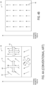
- FIG. 4A shows an example cross-sectional view of a portion of a conventional nanomagnet 40 formed from a crystalline ferromagnetic material.
- the conventional nanomagnet 40 may be a crystalline cobalt nanomagnet.
- the conventional nanomagnet 40 is shown when subjected to an external magnetic field B during manufacturing.
- the external magnetic field B is applied in order to align the magnetic moments 42 within the alloy included in the conventional nanomagnet 40.
- a plurality of crystal grains 41 are shown in FIG. 4A .
- the crystal grains 41 of the conventional nanomagnet 40 exhibit magnetocrystalline anisotropy. Since the crystal structure of cobalt is hexagonal, the magnetocrystalline anisotropy exhibited by the crystal grains 41 of the conventional nanomagnet 40 is uniaxial. Within each of the crystal grains 41, the crystalline cobalt has a respective magnetic easy axis 43.
- the magnetic moments 42 of the atoms included in each of the crystal grains 41 at least partially align with the external magnetic field B when the external magnetic field B is applied.
- the magnetic easy axis 43 of a crystal grain 41 of a crystalline cobalt nanomagnet typically has a coercive field strength of H c ⁇ 100 Oe.
- Each crystal grain 41 also has a magnetic hard axis 44 that is perpendicular to the magnetic easy axis 43 and typically has a coercive field strength of H c > 4000 Oe.
- the conventional nanomagnet 40 generates a nonuniform magnetic field.
- FIG. 4B shows an example cross-sectional view of a portion of the nanomagnet 28 of FIG. 2B .
- the nanomagnet 28 is shown when an external magnetic field B is applied during manufacturing.
- the magnetic moments 45 of the atoms included in the nanomagnet 28 align themselves to the direction of the external magnetic field B without being rotated toward the direction of a magnetic easy axis. Accordingly, the magnetic moments 45 of the atoms included in the nanomagnet 28 are aligned with the external magnetic field B to a greater extent than in the conventional nanomagnet 40 of FIG. 4A .
- the nanomagnet 28 of FIG. 4B therefore exerts a stronger magnetic field on the quantum dots 25 and 26 than the conventional nanomagnet 40 would exert.
- the magnetic field applied to the quantum dots typically has a strength between 0.3 T and 1 T.
- the maximum applied magnetic field reaches a strength between 5 T and 10 T.
- the nanomagnet 28 Since forming the nanomagnet 28 included in a spin-based quantum computing device 20 from an amorphous ferromagnetic alloy such as CoFeB results in an increase in magnetic field strength, splitting between energy levels of the quantum dots 25 and 26 due to the Zeeman effect is also increased.
- the nanomagnet 28 produces a magnetic field of equivalent strength to the magnetic field that would be produced by a conventional nanomagnet 40, except the nanomagnet 28 is smaller in size. This size reduction allows the overall size of the spin-based quantum-dot qubit 22 to be reduced.
- the magnetic field produced by the nanomagnet 28 is decoupled from the crystallographic axes of crystal grains 41, the nanomagnet 28 produces a more uniform magnetic field than the conventional nanomagnet 40 of FIG. 4A . By providing a stronger and more uniform magnetic field than a conventional nanomagnet 40, the nanomagnet 28 discussed above allows the spins of the quantum dots 25 and 26 to be controlled with greater reliability.
Landscapes
- Engineering & Computer Science (AREA)
- General Physics & Mathematics (AREA)
- Theoretical Computer Science (AREA)
- Physics & Mathematics (AREA)
- Power Engineering (AREA)
- Mathematical Analysis (AREA)
- General Engineering & Computer Science (AREA)
- Data Mining & Analysis (AREA)
- Condensed Matter Physics & Semiconductors (AREA)
- Mathematical Optimization (AREA)
- Pure & Applied Mathematics (AREA)
- Computing Systems (AREA)
- Evolutionary Computation (AREA)
- Mathematical Physics (AREA)
- Software Systems (AREA)
- Computational Mathematics (AREA)
- Artificial Intelligence (AREA)
- Thin Magnetic Films (AREA)
- Hall/Mr Elements (AREA)
Abstract
A quantum computing device is provided, including a plurality of spin-based quantum-dot qubits that each include one or more quantum dots. The plurality of spin-based quantum-dot qubits also each include a nanomagnet including an amorphous ferromagnetic alloy.
Description
- The present disclosure relates generally to the field of quantum computing, and more specifically to quantum computing devices that include spin-based quantum-dot qubits.
- In quantum computing devices, computations are performed on information encoded in quantum states known as qubits. In some quantum computing devices, known as spin-based quantum computing devices, qubits are physically instantiated in the spins of charge carriers. The charge carriers may be electrons or electron holes in semiconductor devices. The electrons or electron holes that are used as qubits in spin-based quantum computing devices are confined in quantum dots. When quantum computations are performed, the quantum states of the qubits are modified by influencing the spins of the electrons or electron holes.
- According to one aspect of the present disclosure, a quantum computing device is provided, including a plurality of spin-based quantum-dot qubits that each include one or more quantum dots. The plurality of spin-based quantum-dot qubits also each include a nanomagnet including an amorphous ferromagnetic alloy.
- According to another aspect of the present disclosure, a nanomagnet is provided. The nanomagnet is configured to apply an external magnetic field to one or more quantum dots included in a spin-based quantum computing device. The nanomagnet includes an amorphous ferromagnetic alloy.
- According to another aspect of the present disclosure, a spin-based quantum-dot qubit is provided. The spin-based quantum-dot qubit includes a first silicon layer in which a first quantum dot and a second quantum dot are located. The spin-based quantum-dot qubit further includes a silicon-germanium (SiGe) alloy layer located above the first silicon layer in a thickness direction. The spin-based quantum-dot qubit further includes a second silicon layer located above the SiGe alloy layer in the thickness direction. The spin-based quantum-dot qubit further includes a plurality of plunger gates and a plurality of barrier gates located above the second silicon layer in the thickness direction. The spin-based quantum-dot qubit further includes a nanomagnet located above the plurality of plunger gates and the plurality of barrier gates in the thickness direction. The nanomagnet includes an amorphous ferromagnetic alloy.
-
-
FIG. 1 shows an energy level plot of the energy levels of a quantum dot as a function of magnetic field strength, according to one example. -
FIG. 2A shows an example top view of a quantum computing device including a qubit grid and a measurement device, according to one example. -
FIG. 2B shows the qubit grid ofFIG. 2A in additional detail. -
FIG. 3 shows a vertical cross-sectional view of a spin-based quantum-dot qubit, according to the example ofFIG. 2A . -
FIG. 4A shows an example cross-sectional view of a portion of a conventional nanomagnet formed from a crystalline ferromagnetic material, according to the example ofFIG. 2A . -
FIG. 4B shows an example cross-sectional view of a portion of a nanomagnet including an amorphous ferromagnetic alloy, according to the example ofFIG. 2A . - Spin-based quantum computing devices utilize the Zeeman effect when measuring the spins of charge carriers. The Zeeman effect is an effect on the energy levels of a charged particle that occurs when the particle is subjected to a magnetic field.
FIG. 1 shows anenergy level plot 10 of the energy levels of a quantum dot as a function of magnetic field strength. In the example ofFIG. 1 , an electron is confined within the quantum dot. When the magnetic field is applied, the energy E of the electron confined within the quantum dot splits into two different energy levels. These energy levels correspond to the electron having a spin of 1/2 and a spin of -1/2, respectively. The spins of the electrons confined within quantum dots are controlled in order to perform quantum computations at a quantum computing device. -
FIG. 2A shows an example top view of a portion of aquantum computing device 20, according to one example. Thequantum computing device 20, as shown inFIG. 2A , includes aqubit grid 21 at which a plurality ofqubits 22 are instantiated. Thequbit grid 21 is coupled to ameasurement device 23 that includes a plurality ofmeasurement circuits 24 coupled tocorresponding qubits 22. Thus, themeasurement circuits 24 are configured to obtain classical bits as outputs of quantum computations performed at thequbit grid 21 by measuring the quantum states of thequbits 22. By performing measurements at thequbit grid 21, the quantum states of thequbits 22 are also modified during the execution of quantum algorithms. In some examples, themeasurement circuits 24 are configured to measure tunneling between the quantum dots and respective charge reservoirs. In other examples, themeasurement circuits 24 are configured to obtain charge states that correspond to the spin states of the electrons confined at the quantum dots. - Although, in the example of
FIG. 2A , the plurality ofqubits 22 are arranged in a rectangular grid, the plurality ofqubits 22 may be arranged in some other pattern in other quantum computing device configurations. Additionally or alternatively, other configurations of the plurality ofmeasurement circuits 24 may be used in other example quantum computing devices. -
FIG. 2B shows thequbit grid 21 ofFIG. 2A in additional detail, according to one example. In thequbit grid 21 depicted inFIG. 2B , the plurality ofqubits 22 are spin-based quantum-dot qubits. The spin-based quantum-dot qubits 22 each include one or more quantum dots. In the example ofFIG. 1 , each of the plurality of spin-based quantum-dot qubits 22 is a double-quantum-dot qubit that includes a firstquantum dot 25 and a secondquantum dot 26. In other examples, the spin-based quantum-dot qubits 22 may be single-quantum-dot qubits. - In the
example qubit grid 21 ofFIG. 2B , a plurality ofelectrical leads 27 are electrically coupled to thefirst quantum dot 25 and thesecond quantum dot 26. The electrical leads 27 are configured to apply a voltage to thefirst quantum dot 25 and thesecond quantum dot 26. In addition, a plurality ofgate electrodes 29 are provided at the electrical leads 27, as discussed in further detail below. Thegate electrodes 29 are configured to be opened and closed to adjust the energy levels of thefirst quantum dot 25 and thesecond quantum dot 26. - In the
example qubit grid 21 shown inFIG. 2B , the spin-based quantum-dot qubits 22 further includerespective nanomagnets 28. Thenanomagnets 28 are provided above a surface of thequbit grid 21 in the example ofFIG. 2B . In the example ofFIG. 2B , eachqubit 22 has arespective nanomagnet 28 located above it. In other examples, a plurality of thequbits 22 have a shared nanomagnet. Via thenanomagnet 28, thefirst quantum dot 25 and thesecond quantum dot 26 are subjected to a magnetic field that produces the energy level splitting discussed above with reference toFIG. 1 . - In some examples, during manufacturing of the
quantum computing device 20, thenanomagnets 28 are formed via sputter deposition. Thenanomagnets 28 may be subjected to an external magnetic field when sputter deposition is performed in order to align the magnetic moments of the atoms included in thenanomagnets 28, as discussed in further detail below. -
FIG. 3 shows a vertical cross-sectional view of a spin-based quantum-dot qubit 22 included in thequantum computing device 20, according to one example. In the example ofFIG. 3 , the spin-based quantum-dot qubit 22 includes a stack of a plurality of layers. Athickness direction 30 of the stack is shown inFIG. 3 . - The plurality of layers includes one or more silicon layers. According to the example of
FIG. 3 , the spin-based quantum-dot qubit 22 includes asubstrate layer 31. The substrate layer may, for example, be formed from, and thus include, silicon. - The spin-based
quantum dot qubit 22 further includes abuffer layer 32 located above thesubstrate layer 31 in thethickness direction 30. The buffer layer may be a silicon-germanium (SiGe) alloy layer, which may, for example, include an SiGe alloy having a composition of Si0.7Ge0.3. In other examples, thebuffer layer 32 may have some other composition. Thebuffer layer 32 provides electron confinement between layers of the spin-basedquantum dot qubit 22. - The spin-based
quantum dot qubit 22 further includes aquantum well layer 33 located above thebuffer layer 32 in thethickness direction 30. Thefirst quantum dot 25 and thesecond quantum dot 26 are located in thequantum well layer 33. For example, thequantum well layer 33 may be a silicon layer. - In examples in which the
buffer layer 32 is an SiGe alloy layer, the ratio of silicon to germanium is selected such that electron confinement in thequantum well layer 33 is balanced with material strain. Electron confinement increases with increasing levels of germanium. Material strain decreases with increasing levels of silicon, thereby reducing a dislocation density of thebuffer layer 32. The example composition Si0.7Ge0.3 discussed above provides both a high level of electron confinement and a low dislocation density. - The spin-based
quantum dot qubit 22 shown inFIG. 3 further includes atop barrier layer 34 located above the quantum well layer in thethickness direction 30. Similarly to thebuffer layer 32, thetop barrier layer 34 provides electron confinement between layers of the spin-basedquantum dot qubit 22. Thetop barrier layer 34 may be an SiGe layer and may, for example, have the composition Si0.7Ge0.3. - The spin-based
quantum dot qubit 22 further includes agate dielectric layer 35 located above thetop barrier layer 34 in thethickness direction 30. Thegate dielectric layer 35 is an insulator that insulates the electrical leads 27 and thegate electrodes 29 from thetop barrier layer 34. For example, thegate dielectric layer 35 may be a silicon dioxide (SiO2) layer. - The spin-based
quantum dot qubit 22 further includes a plurality of electrode gates located above thegate dielectric layer 35 in thethickness direction 30. The plurality ofgate electrodes 29 includes a plurality ofplunger gates 29A and a plurality ofbarrier gates 29B. In addition, a source lead 27A and adrain lead 27B are located above thesecond silicon layer 33 in thethickness direction 30. The source lead 27A and thedrain lead 27B are the electrical leads via which electrons are transferred between the quantum dots and an electron source area. The source lead 27A and thedrain lead 27B are respectively configured to provide electrons to the quantum dots and receive electrons from the quantum dots. The electron source area is an implanted area of thequbit grid 21 in some examples. - As discussed above with reference to
FIG. 2B , the spin-based quantum-dot qubit 22 further includes ananomagnet 28 located above the plurality ofplunger gates 29A and the plurality ofbarrier gates 29B in thethickness direction 30. Thus, thenanomagnet 28 is located in a layer of thequantum computing device 20 provided above thequantum dots thickness direction 30, and is located on an opposite side of thesubstrate layer 31 relative to thequantum dots - The
nanomagnet 28 includes an amorphous ferromagnetic alloy. As shown in the example ofFIG. 3 , the amorphous ferromagnetic alloy is a cobalt-iron-boron (CoFeB) alloy. In this example, the CoFeB alloy has a composition of Co1-xFexBy, with 0 < x < 1 and 0.2 < y < 1. - Using an alloy rather than an elemental material as the material of the
nanomagnet 28 allows a stronger magnetic field to be achieved.FIG. 4A shows an example cross-sectional view of a portion of aconventional nanomagnet 40 formed from a crystalline ferromagnetic material. For example, theconventional nanomagnet 40 may be a crystalline cobalt nanomagnet. Theconventional nanomagnet 40 is shown when subjected to an external magnetic field B during manufacturing. The external magnetic field B is applied in order to align themagnetic moments 42 within the alloy included in theconventional nanomagnet 40. - A plurality of
crystal grains 41 are shown inFIG. 4A . Thecrystal grains 41 of theconventional nanomagnet 40 exhibit magnetocrystalline anisotropy. Since the crystal structure of cobalt is hexagonal, the magnetocrystalline anisotropy exhibited by thecrystal grains 41 of theconventional nanomagnet 40 is uniaxial. Within each of thecrystal grains 41, the crystalline cobalt has a respective magneticeasy axis 43. Themagnetic moments 42 of the atoms included in each of thecrystal grains 41 at least partially align with the external magnetic field B when the external magnetic field B is applied. - The magnetic
easy axis 43 of acrystal grain 41 of a crystalline cobalt nanomagnet typically has a coercive field strength of Hc < 100 Oe. Eachcrystal grain 41 also has a magnetichard axis 44 that is perpendicular to the magneticeasy axis 43 and typically has a coercive field strength of Hc > 4000 Oe. In addition, due to the variability in the angles of themagnetic moments 42, theconventional nanomagnet 40 generates a nonuniform magnetic field. -
FIG. 4B shows an example cross-sectional view of a portion of thenanomagnet 28 ofFIG. 2B . Similarly to in the example ofFIG. 4A , thenanomagnet 28 is shown when an external magnetic field B is applied during manufacturing. As shown in the example ofFIG. 4B , since thenanomagnet 28 is formed from an amorphous ferromagnetic alloy, themagnetic moments 45 of the atoms included in thenanomagnet 28 align themselves to the direction of the external magnetic field B without being rotated toward the direction of a magnetic easy axis. Accordingly, themagnetic moments 45 of the atoms included in thenanomagnet 28 are aligned with the external magnetic field B to a greater extent than in theconventional nanomagnet 40 ofFIG. 4A . Thenanomagnet 28 ofFIG. 4B therefore exerts a stronger magnetic field on thequantum dots conventional nanomagnet 40 would exert. During qubit operations performed at thequantum computing device 20, the magnetic field applied to the quantum dots typically has a strength between 0.3 T and 1 T. In some experiments performed at thequantum computing device 20, the maximum applied magnetic field reaches a strength between 5 T and 10 T. - Since forming the
nanomagnet 28 included in a spin-basedquantum computing device 20 from an amorphous ferromagnetic alloy such as CoFeB results in an increase in magnetic field strength, splitting between energy levels of thequantum dots nanomagnet 28 produces a magnetic field of equivalent strength to the magnetic field that would be produced by aconventional nanomagnet 40, except thenanomagnet 28 is smaller in size. This size reduction allows the overall size of the spin-based quantum-dot qubit 22 to be reduced. In addition, since the magnetic field produced by thenanomagnet 28 is decoupled from the crystallographic axes ofcrystal grains 41, thenanomagnet 28 produces a more uniform magnetic field than theconventional nanomagnet 40 ofFIG. 4A . By providing a stronger and more uniform magnetic field than aconventional nanomagnet 40, thenanomagnet 28 discussed above allows the spins of thequantum dots - Further, the disclosure comprises configurations according to the following clauses.
-
Clause 1. A quantum computing device comprising: a plurality of spin-based quantum-dot qubits that each include: one or more quantum dots; and a nanomagnet including an amorphous ferromagnetic alloy. -
Clause 2. The quantum computing device ofclause 1, wherein the amorphous ferromagnetic alloy is a cobalt-iron-boron (CoFeB) alloy. - Clause 3. The quantum computing device of
clause 2, wherein the CoFeB alloy has a composition of Co1-xFexBy, with 0 < x < 1 and 0.2 < y < 1. - Clause 4. The quantum computing device of
clause 1, wherein: each of the plurality of spin-based quantum-dot qubits includes a stack of a plurality of layers, the stack having a thickness direction; and the nanomagnet is located in a layer of the plurality of layers that is provided above the one or more quantum dots in the thickness direction. - Clause 5. The quantum computing device of
clause 1, wherein each of the plurality of spin-based quantum-dot qubits is a double-quantum-dot qubit that includes a first quantum dot and a second quantum dot. - Clause 6. The quantum computing device of
clause 1, wherein each of the spin-based quantum-dot qubits further includes a plurality of barrier gates. - Clause 7. The quantum computing device of
clause 1, wherein each of the spin-based quantum-dot qubits further includes a plurality of plunger gates. - Clause 8. The quantum computing device of
clause 1, wherein each of the spin-based quantum-dot qubits further includes one or more silicon layers. - Clause 9. The quantum computing device of
clause 1, wherein each of the spin-based quantum-dot qubits further includes one or more silicon-germanium (SiGe) alloy layers. -
Clause 10. The quantum computing device ofclause 1, wherein the one or more quantum dots are formed from silicon. - Clause 11. The quantum computing device of
clause 1, wherein the nanomagnet is formed via sputtering. - Clause 12. A nanomagnet configured to apply an external magnetic field to one or more quantum dots included in a spin-based quantum computing device, wherein the nanomagnet includes an amorphous ferromagnetic alloy.
- Clause 13. The nanomagnet of clause 12, wherein the amorphous ferromagnetic alloy is a cobalt-iron-boron (CoFeB) alloy.
- Clause 14. The nanomagnet of clause 13, wherein the CoFeB alloy has a composition of Co1-xFexBy, with 0 < x < 1 and 0.2 < y < 1.
- Clause 15. The nanomagnet of clause 12, wherein the nanomagnet is located in a layer of the spin-based quantum computing device provided above the one or more quantum dots in a thickness direction.
- Clause 16. The nanomagnet of clause 15, wherein the nanomagnet is located on an opposite side of a substrate layer relative to the one or more quantum dots.
- Clause 17. The nanomagnet of clause 12, wherein the nanomagnet is formed via sputtering.
- Clause 18. A spin-based quantum-dot qubit that includes: a substrate layer; a buffer layer located above the substrate layer in a thickness direction; a quantum well layer in which a first quantum dot and a second quantum dot are located, wherein the quantum well layer is located above the buffer layer in the thickness direction; a top barrier layer located above the quantum well layer in the thickness direction; a gate dielectric layer located above the top barrier layer in the thickness direction; a plurality of plunger gates and a plurality of barrier gates located above the gate dielectric layer in the thickness direction; and a nanomagnet located above the plurality of plunger gates and the plurality of barrier gates in the thickness direction, wherein the nanomagnet includes an amorphous ferromagnetic alloy.
- Clause 19. The spin-based quantum-dot qubit of clause 18, wherein the amorphous ferromagnetic alloy is a cobalt-iron-boron (CoFeB) alloy.
-
Clause 20. The spin-based quantum-dot qubit of clause 19, wherein the CoFeB alloy has a composition of Co1-xFexBy, with 0 < x < 1 and 0.2 < y < 1.
Claims (15)
- A nanomagnet (28), configured to apply an external magnetic field to one or more quantum dots (25, 26) included in a spin-based quantum computing device (20), wherein the nanomagnet (28) includes an amorphous ferromagnetic alloy.
- The nanomagnet (28) of claim 1, wherein the amorphous ferromagnetic alloy is a cobalt-iron-boron (CoFeB) alloy.
- The nanomagnet (28) of claim 2, wherein the CoFeB alloy has a composition of Co1-xFexBy, with 0 < x < 1 and 0.2 < y < 1.
- The nanomagnet (28) of any one of claims 1-3, wherein the nanomagnet is formed via sputtering.
- A quantum computing device (20), comprising:
a plurality of spin-based quantum-dot qubits (22) that each includes:one or more quantum dots (25, 26); anda nanomagnet (28) according to any one of claims 1 to 4. - The quantum computing device (20) of claim 5, wherein:each of the plurality of spin-based quantum-dot qubits (22) includes a stack of a plurality of layers (31, 32, 33, 34, 35), the stack having a thickness direction (30); andthe nanomagnet (28) is located in a layer of the plurality of layers that is provided above the one or more quantum dots (25, 26) in the thickness direction (30).
- The quantum computing device (20) of any one of claims 5 or 6, wherein each of the plurality of spin-based quantum-dot qubits (22) is a double-quantum-dot qubit that includes a first quantum dot (25) and a second quantum dot (26).
- The quantum computing device (20) of any one of claims 5-7, wherein each of the spin-based quantum-dot qubits (22) further includes a plurality of barrier gates (29B).
- The quantum computing device (20) of any one of claims 5-8, wherein each of the spin-based quantum-dot qubits (22) further includes a plurality of plunger gates (29A).
- The quantum computing device (20) of any one of claims 5-9, wherein each of the spin-based quantum-dot qubits (22) further includes one or more silicon layers.
- The quantum computing device (20) of any one of claims 5-10, wherein each of the spin-based quantum-dot qubits (22) further includes one or more silicon-germanium (SiGe) alloy layers.
- The quantum computing device (20) of any one of claims 5-11, wherein the one or more quantum dots (25, 26) are formed from silicon.
- The quantum computing device (20) of claim 6, wherein the nanomagnet (28) is located on an opposite side of a substrate layer (31) relative to the one or more quantum dots (25, 26).
- The quantum computing device (20) of any one of claims 5-13, wherein the nanomagnet (28) applies a magnetic field to the quantum dots (25, 26) in the range of 0.3 T and 10 T.
- A spin-based quantum-dot qubit (22), comprising:a substrate layer (31);a buffer layer (32) located above the substrate layer (31) in a thickness direction (30);a quantum well layer (33) in which a first quantum dot (25) and a second quantum dot (26) are located, wherein the quantum well layer (33) is located above the buffer layer (32) in the thickness direction (30);a top barrier layer (34) located above the quantum well layer (33) in the thickness direction (30);a gate dielectric layer (35) located above the top barrier layer (34) in the thickness direction (30);a plurality of plunger gates (29A) and a plurality of barrier gates (29B) located above the gate dielectric layer (35) in the thickness direction (30); anda nanomagnet (28) located above the plurality of plunger gates (29A) and the plurality of barrier gates (29B) in the thickness direction (30), wherein the nanomagnet (28) is according to any one of claims 1 to 4.
Applications Claiming Priority (1)
| Application Number | Priority Date | Filing Date | Title |
|---|---|---|---|
| US18/359,327 US20250037917A1 (en) | 2023-07-26 | 2023-07-26 | Nanomagnet for spin-based quantum-dot qubit |
Publications (1)
| Publication Number | Publication Date |
|---|---|
| EP4498406A1 true EP4498406A1 (en) | 2025-01-29 |
Family
ID=91027212
Family Applications (1)
| Application Number | Title | Priority Date | Filing Date |
|---|---|---|---|
| EP24174351.7A Pending EP4498406A1 (en) | 2023-07-26 | 2024-05-06 | Nanomagnet for spin-based quantum-dot qubit |
Country Status (6)
| Country | Link |
|---|---|
| US (1) | US20250037917A1 (en) |
| EP (1) | EP4498406A1 (en) |
| JP (1) | JP2025018908A (en) |
| CN (1) | CN119378703A (en) |
| AU (1) | AU2024205124A1 (en) |
| TW (1) | TW202522519A (en) |
Citations (2)
| Publication number | Priority date | Publication date | Assignee | Title |
|---|---|---|---|---|
| US20190044048A1 (en) * | 2018-02-08 | 2019-02-07 | Intel Corporation | Sidewall metal spacers for forming metal gates in quantum devices |
| US20220222564A1 (en) * | 2019-04-15 | 2022-07-14 | National Institute Of Advanced Industrial Science And Technology | Quantum bit cell and quantum bit integrated circuit |
Family Cites Families (4)
| Publication number | Priority date | Publication date | Assignee | Title |
|---|---|---|---|---|
| US8470462B2 (en) * | 2010-11-30 | 2013-06-25 | Magic Technologies, Inc. | Structure and method for enhancing interfacial perpendicular anisotropy in CoFe(B)/MgO/CoFe(B) magnetic tunnel junctions |
| US9053719B2 (en) * | 2012-11-30 | 2015-06-09 | Western Digital (Fremont), Llc | Magnetoresistive sensor for a magnetic storage system read head, and fabrication method thereof |
| EP3967650A1 (en) * | 2020-09-15 | 2022-03-16 | Imec VZW | A qubit device and a method for operating a qubit device |
| FR3137197B1 (en) * | 2022-06-23 | 2024-09-06 | Commissariat Energie Atomique | Spin qubit electronic device |
-
2023
- 2023-07-26 US US18/359,327 patent/US20250037917A1/en active Pending
-
2024
- 2024-04-11 JP JP2024063905A patent/JP2025018908A/en active Pending
- 2024-05-06 EP EP24174351.7A patent/EP4498406A1/en active Pending
- 2024-05-07 TW TW113116855A patent/TW202522519A/en unknown
- 2024-07-25 CN CN202411004585.4A patent/CN119378703A/en active Pending
- 2024-07-26 AU AU2024205124A patent/AU2024205124A1/en active Pending
Patent Citations (2)
| Publication number | Priority date | Publication date | Assignee | Title |
|---|---|---|---|---|
| US20190044048A1 (en) * | 2018-02-08 | 2019-02-07 | Intel Corporation | Sidewall metal spacers for forming metal gates in quantum devices |
| US20220222564A1 (en) * | 2019-04-15 | 2022-07-14 | National Institute Of Advanced Industrial Science And Technology | Quantum bit cell and quantum bit integrated circuit |
Non-Patent Citations (2)
| Title |
|---|
| CHEN YUAN-TSUNG ET AL: "Magnetic and Electric Properties of Amorphous Co 40 Fe 40 B 20 Thin Films", JOURNAL OF NANOMATERIALS, vol. 2012, no. 1, 1 January 2012 (2012-01-01), US, XP093206500, ISSN: 1687-4110, Retrieved from the Internet <URL:http://downloads.hindawi.com/journals/jnm/2012/486284.xml> DOI: 10.1155/2012/486284 * |
| CIUREANU M ET AL: "Magnetic properties of electrodeposited CoFeB thin films and nanowire arrays", ELECTROCHIMICA ACTA, ELSEVIER, AMSTERDAM, NL, vol. 50, no. 22, 10 August 2005 (2005-08-10), pages 4487 - 4497, XP027693909, ISSN: 0013-4686, [retrieved on 20050810] * |
Also Published As
| Publication number | Publication date |
|---|---|
| TW202522519A (en) | 2025-06-01 |
| AU2024205124A1 (en) | 2025-02-13 |
| US20250037917A1 (en) | 2025-01-30 |
| JP2025018908A (en) | 2025-02-06 |
| CN119378703A (en) | 2025-01-28 |
Similar Documents
| Publication | Publication Date | Title |
|---|---|---|
| US7994555B2 (en) | Spin transistor using perpendicular magnetization | |
| US8609262B2 (en) | Structure and method to fabricate high performance MTJ devices for spin-transfer torque (STT)-RAM application | |
| KR101985695B1 (en) | Writable magnetic element | |
| US8138561B2 (en) | Structure and method to fabricate high performance MTJ devices for spin-transfer torque (STT)-RAM | |
| US7861401B2 (en) | Method of forming a high performance tunneling magnetoresistive (TMR) element | |
| US9006704B2 (en) | Magnetic element with improved out-of-plane anisotropy for spintronic applications | |
| US5841692A (en) | Magnetic tunnel junction device with antiferromagnetically coupled pinned layer | |
| US8779538B2 (en) | Magnetic tunneling junction seed, capping, and spacer layer materials | |
| US9385304B2 (en) | Magnetic memory and method of manufacturing the same | |
| Cai et al. | Selective operations of multi-pillar SOT-MRAM for high density and low power embedded memories | |
| US20120280336A1 (en) | Multilayers having reduced perpendicular demagnetizing field using moment dilution for spintronic applications | |
| US8217477B2 (en) | Magnetic memory cell and magnetic random access memory | |
| EP1793434A1 (en) | Magnetoresistacne element and production method therefor | |
| US7211447B2 (en) | Structure and method to fabricate high performance MTJ devices for MRAM applications | |
| DE602006000836T2 (en) | Line control arrangement | |
| Takahashi et al. | Ion-beam-etched profile control of MTJ cells for improving the switching characteristics of high-density MRAM | |
| US7208807B2 (en) | Structure and method to fabricate high performance MTJ devices for MRAM applications | |
| US20250037917A1 (en) | Nanomagnet for spin-based quantum-dot qubit | |
| US10374147B2 (en) | Perpendicular magnetic tunnel junction having improved reference layer stability | |
| WO2007148854A9 (en) | Spin transistor using ferromagnet | |
| US12230307B2 (en) | Performance of magnetic channel junctions | |
| Marukame et al. | Read/write operation of spin-based MOSFET using highly spin-polarized ferromagnet/MgO tunnel barrier for reconfigurable logic devices | |
| US20200058846A1 (en) | Magnetic tunnel junction device and magnetic resistance memory device | |
| US12557294B1 (en) | Magnetoresistive random access memory | |
| Karki | New materials for magnetic tunnel junction devices for neuromorphic and probabilistic computing |
Legal Events
| Date | Code | Title | Description |
|---|---|---|---|
| PUAI | Public reference made under article 153(3) epc to a published international application that has entered the european phase |
Free format text: ORIGINAL CODE: 0009012 |
|
| STAA | Information on the status of an ep patent application or granted ep patent |
Free format text: STATUS: THE APPLICATION HAS BEEN PUBLISHED |
|
| AK | Designated contracting states |
Kind code of ref document: A1 Designated state(s): AL AT BE BG CH CY CZ DE DK EE ES FI FR GB GR HR HU IE IS IT LI LT LU LV MC ME MK MT NL NO PL PT RO RS SE SI SK SM TR |
|
| STAA | Information on the status of an ep patent application or granted ep patent |
Free format text: STATUS: REQUEST FOR EXAMINATION WAS MADE |
|
| 17P | Request for examination filed |
Effective date: 20250728 |