EP4498354A2 - Pixel circuit for wide brightness range display - Google Patents
Pixel circuit for wide brightness range display Download PDFInfo
- Publication number
- EP4498354A2 EP4498354A2 EP24183297.1A EP24183297A EP4498354A2 EP 4498354 A2 EP4498354 A2 EP 4498354A2 EP 24183297 A EP24183297 A EP 24183297A EP 4498354 A2 EP4498354 A2 EP 4498354A2
- Authority
- EP
- European Patent Office
- Prior art keywords
- transistor
- emission control
- coupled
- terminal
- driving
- Prior art date
- Legal status (The legal status is an assumption and is not a legal conclusion. Google has not performed a legal analysis and makes no representation as to the accuracy of the status listed.)
- Pending
Links
Images






Classifications
-
- G—PHYSICS
- G09—EDUCATION; CRYPTOGRAPHY; DISPLAY; ADVERTISING; SEALS
- G09G—ARRANGEMENTS OR CIRCUITS FOR CONTROL OF INDICATING DEVICES USING STATIC MEANS TO PRESENT VARIABLE INFORMATION
- G09G3/00—Control arrangements or circuits, of interest only in connection with visual indicators other than cathode-ray tubes
- G09G3/20—Control arrangements or circuits, of interest only in connection with visual indicators other than cathode-ray tubes for presentation of an assembly of a number of characters, e.g. a page, by composing the assembly by combination of individual elements arranged in a matrix no fixed position being assigned to or needed to be assigned to the individual characters or partial characters
- G09G3/22—Control arrangements or circuits, of interest only in connection with visual indicators other than cathode-ray tubes for presentation of an assembly of a number of characters, e.g. a page, by composing the assembly by combination of individual elements arranged in a matrix no fixed position being assigned to or needed to be assigned to the individual characters or partial characters using controlled light sources
- G09G3/30—Control arrangements or circuits, of interest only in connection with visual indicators other than cathode-ray tubes for presentation of an assembly of a number of characters, e.g. a page, by composing the assembly by combination of individual elements arranged in a matrix no fixed position being assigned to or needed to be assigned to the individual characters or partial characters using controlled light sources using electroluminescent panels
- G09G3/32—Control arrangements or circuits, of interest only in connection with visual indicators other than cathode-ray tubes for presentation of an assembly of a number of characters, e.g. a page, by composing the assembly by combination of individual elements arranged in a matrix no fixed position being assigned to or needed to be assigned to the individual characters or partial characters using controlled light sources using electroluminescent panels semiconductive, e.g. using light-emitting diodes [LED]
-
- G—PHYSICS
- G09—EDUCATION; CRYPTOGRAPHY; DISPLAY; ADVERTISING; SEALS
- G09G—ARRANGEMENTS OR CIRCUITS FOR CONTROL OF INDICATING DEVICES USING STATIC MEANS TO PRESENT VARIABLE INFORMATION
- G09G3/00—Control arrangements or circuits, of interest only in connection with visual indicators other than cathode-ray tubes
- G09G3/20—Control arrangements or circuits, of interest only in connection with visual indicators other than cathode-ray tubes for presentation of an assembly of a number of characters, e.g. a page, by composing the assembly by combination of individual elements arranged in a matrix no fixed position being assigned to or needed to be assigned to the individual characters or partial characters
- G09G3/2092—Details of a display terminals using a flat panel, the details relating to the control arrangement of the display terminal and to the interfaces thereto
- G09G3/2096—Details of the interface to the display terminal specific for a flat panel
-
- G—PHYSICS
- G09—EDUCATION; CRYPTOGRAPHY; DISPLAY; ADVERTISING; SEALS
- G09G—ARRANGEMENTS OR CIRCUITS FOR CONTROL OF INDICATING DEVICES USING STATIC MEANS TO PRESENT VARIABLE INFORMATION
- G09G3/00—Control arrangements or circuits, of interest only in connection with visual indicators other than cathode-ray tubes
- G09G3/20—Control arrangements or circuits, of interest only in connection with visual indicators other than cathode-ray tubes for presentation of an assembly of a number of characters, e.g. a page, by composing the assembly by combination of individual elements arranged in a matrix no fixed position being assigned to or needed to be assigned to the individual characters or partial characters
- G09G3/22—Control arrangements or circuits, of interest only in connection with visual indicators other than cathode-ray tubes for presentation of an assembly of a number of characters, e.g. a page, by composing the assembly by combination of individual elements arranged in a matrix no fixed position being assigned to or needed to be assigned to the individual characters or partial characters using controlled light sources
- G09G3/30—Control arrangements or circuits, of interest only in connection with visual indicators other than cathode-ray tubes for presentation of an assembly of a number of characters, e.g. a page, by composing the assembly by combination of individual elements arranged in a matrix no fixed position being assigned to or needed to be assigned to the individual characters or partial characters using controlled light sources using electroluminescent panels
- G09G3/32—Control arrangements or circuits, of interest only in connection with visual indicators other than cathode-ray tubes for presentation of an assembly of a number of characters, e.g. a page, by composing the assembly by combination of individual elements arranged in a matrix no fixed position being assigned to or needed to be assigned to the individual characters or partial characters using controlled light sources using electroluminescent panels semiconductive, e.g. using light-emitting diodes [LED]
- G09G3/3208—Control arrangements or circuits, of interest only in connection with visual indicators other than cathode-ray tubes for presentation of an assembly of a number of characters, e.g. a page, by composing the assembly by combination of individual elements arranged in a matrix no fixed position being assigned to or needed to be assigned to the individual characters or partial characters using controlled light sources using electroluminescent panels semiconductive, e.g. using light-emitting diodes [LED] organic, e.g. using organic light-emitting diodes [OLED]
- G09G3/3225—Control arrangements or circuits, of interest only in connection with visual indicators other than cathode-ray tubes for presentation of an assembly of a number of characters, e.g. a page, by composing the assembly by combination of individual elements arranged in a matrix no fixed position being assigned to or needed to be assigned to the individual characters or partial characters using controlled light sources using electroluminescent panels semiconductive, e.g. using light-emitting diodes [LED] organic, e.g. using organic light-emitting diodes [OLED] using an active matrix
- G09G3/3233—Control arrangements or circuits, of interest only in connection with visual indicators other than cathode-ray tubes for presentation of an assembly of a number of characters, e.g. a page, by composing the assembly by combination of individual elements arranged in a matrix no fixed position being assigned to or needed to be assigned to the individual characters or partial characters using controlled light sources using electroluminescent panels semiconductive, e.g. using light-emitting diodes [LED] organic, e.g. using organic light-emitting diodes [OLED] using an active matrix with pixel circuitry controlling the current through the light-emitting element
-
- G—PHYSICS
- G09—EDUCATION; CRYPTOGRAPHY; DISPLAY; ADVERTISING; SEALS
- G09G—ARRANGEMENTS OR CIRCUITS FOR CONTROL OF INDICATING DEVICES USING STATIC MEANS TO PRESENT VARIABLE INFORMATION
- G09G3/00—Control arrangements or circuits, of interest only in connection with visual indicators other than cathode-ray tubes
- G09G3/20—Control arrangements or circuits, of interest only in connection with visual indicators other than cathode-ray tubes for presentation of an assembly of a number of characters, e.g. a page, by composing the assembly by combination of individual elements arranged in a matrix no fixed position being assigned to or needed to be assigned to the individual characters or partial characters
- G09G3/22—Control arrangements or circuits, of interest only in connection with visual indicators other than cathode-ray tubes for presentation of an assembly of a number of characters, e.g. a page, by composing the assembly by combination of individual elements arranged in a matrix no fixed position being assigned to or needed to be assigned to the individual characters or partial characters using controlled light sources
- G09G3/30—Control arrangements or circuits, of interest only in connection with visual indicators other than cathode-ray tubes for presentation of an assembly of a number of characters, e.g. a page, by composing the assembly by combination of individual elements arranged in a matrix no fixed position being assigned to or needed to be assigned to the individual characters or partial characters using controlled light sources using electroluminescent panels
- G09G3/32—Control arrangements or circuits, of interest only in connection with visual indicators other than cathode-ray tubes for presentation of an assembly of a number of characters, e.g. a page, by composing the assembly by combination of individual elements arranged in a matrix no fixed position being assigned to or needed to be assigned to the individual characters or partial characters using controlled light sources using electroluminescent panels semiconductive, e.g. using light-emitting diodes [LED]
- G09G3/3208—Control arrangements or circuits, of interest only in connection with visual indicators other than cathode-ray tubes for presentation of an assembly of a number of characters, e.g. a page, by composing the assembly by combination of individual elements arranged in a matrix no fixed position being assigned to or needed to be assigned to the individual characters or partial characters using controlled light sources using electroluminescent panels semiconductive, e.g. using light-emitting diodes [LED] organic, e.g. using organic light-emitting diodes [OLED]
- G09G3/3266—Details of drivers for scan electrodes
-
- G—PHYSICS
- G09—EDUCATION; CRYPTOGRAPHY; DISPLAY; ADVERTISING; SEALS
- G09G—ARRANGEMENTS OR CIRCUITS FOR CONTROL OF INDICATING DEVICES USING STATIC MEANS TO PRESENT VARIABLE INFORMATION
- G09G2300/00—Aspects of the constitution of display devices
- G09G2300/08—Active matrix structure, i.e. with use of active elements, inclusive of non-linear two terminal elements, in the pixels together with light emitting or modulating elements
- G09G2300/0809—Several active elements per pixel in active matrix panels
- G09G2300/0819—Several active elements per pixel in active matrix panels used for counteracting undesired variations, e.g. feedback or autozeroing
-
- G—PHYSICS
- G09—EDUCATION; CRYPTOGRAPHY; DISPLAY; ADVERTISING; SEALS
- G09G—ARRANGEMENTS OR CIRCUITS FOR CONTROL OF INDICATING DEVICES USING STATIC MEANS TO PRESENT VARIABLE INFORMATION
- G09G2300/00—Aspects of the constitution of display devices
- G09G2300/08—Active matrix structure, i.e. with use of active elements, inclusive of non-linear two terminal elements, in the pixels together with light emitting or modulating elements
- G09G2300/0809—Several active elements per pixel in active matrix panels
- G09G2300/0842—Several active elements per pixel in active matrix panels forming a memory circuit, e.g. a dynamic memory with one capacitor
-
- G—PHYSICS
- G09—EDUCATION; CRYPTOGRAPHY; DISPLAY; ADVERTISING; SEALS
- G09G—ARRANGEMENTS OR CIRCUITS FOR CONTROL OF INDICATING DEVICES USING STATIC MEANS TO PRESENT VARIABLE INFORMATION
- G09G2300/00—Aspects of the constitution of display devices
- G09G2300/08—Active matrix structure, i.e. with use of active elements, inclusive of non-linear two terminal elements, in the pixels together with light emitting or modulating elements
- G09G2300/0809—Several active elements per pixel in active matrix panels
- G09G2300/0842—Several active elements per pixel in active matrix panels forming a memory circuit, e.g. a dynamic memory with one capacitor
- G09G2300/0852—Several active elements per pixel in active matrix panels forming a memory circuit, e.g. a dynamic memory with one capacitor being a dynamic memory with more than one capacitor
-
- G—PHYSICS
- G09—EDUCATION; CRYPTOGRAPHY; DISPLAY; ADVERTISING; SEALS
- G09G—ARRANGEMENTS OR CIRCUITS FOR CONTROL OF INDICATING DEVICES USING STATIC MEANS TO PRESENT VARIABLE INFORMATION
- G09G2300/00—Aspects of the constitution of display devices
- G09G2300/08—Active matrix structure, i.e. with use of active elements, inclusive of non-linear two terminal elements, in the pixels together with light emitting or modulating elements
- G09G2300/0809—Several active elements per pixel in active matrix panels
- G09G2300/0842—Several active elements per pixel in active matrix panels forming a memory circuit, e.g. a dynamic memory with one capacitor
- G09G2300/0861—Several active elements per pixel in active matrix panels forming a memory circuit, e.g. a dynamic memory with one capacitor with additional control of the display period without amending the charge stored in a pixel memory, e.g. by means of additional select electrodes
-
- G—PHYSICS
- G09—EDUCATION; CRYPTOGRAPHY; DISPLAY; ADVERTISING; SEALS
- G09G—ARRANGEMENTS OR CIRCUITS FOR CONTROL OF INDICATING DEVICES USING STATIC MEANS TO PRESENT VARIABLE INFORMATION
- G09G2310/00—Command of the display device
- G09G2310/02—Addressing, scanning or driving the display screen or processing steps related thereto
- G09G2310/0262—The addressing of the pixel, in a display other than an active matrix LCD, involving the control of two or more scan electrodes or two or more data electrodes, e.g. pixel voltage dependent on signals of two data electrodes
-
- G—PHYSICS
- G09—EDUCATION; CRYPTOGRAPHY; DISPLAY; ADVERTISING; SEALS
- G09G—ARRANGEMENTS OR CIRCUITS FOR CONTROL OF INDICATING DEVICES USING STATIC MEANS TO PRESENT VARIABLE INFORMATION
- G09G2310/00—Command of the display device
- G09G2310/08—Details of timing specific for flat panels, other than clock recovery
-
- G—PHYSICS
- G09—EDUCATION; CRYPTOGRAPHY; DISPLAY; ADVERTISING; SEALS
- G09G—ARRANGEMENTS OR CIRCUITS FOR CONTROL OF INDICATING DEVICES USING STATIC MEANS TO PRESENT VARIABLE INFORMATION
- G09G2320/00—Control of display operating conditions
- G09G2320/02—Improving the quality of display appearance
- G09G2320/0233—Improving the luminance or brightness uniformity across the screen
-
- G—PHYSICS
- G09—EDUCATION; CRYPTOGRAPHY; DISPLAY; ADVERTISING; SEALS
- G09G—ARRANGEMENTS OR CIRCUITS FOR CONTROL OF INDICATING DEVICES USING STATIC MEANS TO PRESENT VARIABLE INFORMATION
- G09G2320/00—Control of display operating conditions
- G09G2320/04—Maintaining the quality of display appearance
- G09G2320/043—Preventing or counteracting the effects of ageing
- G09G2320/045—Compensation of drifts in the characteristics of light emitting or modulating elements
-
- G—PHYSICS
- G09—EDUCATION; CRYPTOGRAPHY; DISPLAY; ADVERTISING; SEALS
- G09G—ARRANGEMENTS OR CIRCUITS FOR CONTROL OF INDICATING DEVICES USING STATIC MEANS TO PRESENT VARIABLE INFORMATION
- G09G2320/00—Control of display operating conditions
- G09G2320/06—Adjustment of display parameters
- G09G2320/0626—Adjustment of display parameters for control of overall brightness
-
- G—PHYSICS
- G09—EDUCATION; CRYPTOGRAPHY; DISPLAY; ADVERTISING; SEALS
- G09G—ARRANGEMENTS OR CIRCUITS FOR CONTROL OF INDICATING DEVICES USING STATIC MEANS TO PRESENT VARIABLE INFORMATION
- G09G2360/00—Aspects of the architecture of display systems
- G09G2360/14—Detecting light within display terminals, e.g. using a single or a plurality of photosensors
- G09G2360/144—Detecting light within display terminals, e.g. using a single or a plurality of photosensors the light being ambient light
Definitions
- the disclosure relates to pixel circuits, and more particularly to pixel circuits and driving schemes for wide brightness range.
- a pixel circuit is a circuit that controls the brightness of a pixel on a display.
- each pixel has its own transistor.
- the transistor is used to control the flow of current to the pixel.
- the transistor is turned on and off by a digital signal. When the transistor is turned on, current can flow through the pixel causing the pixel to light up. When the transistor is turned off, current cannot flow through the pixel, and the pixel turns off.
- a pixel circuit driving scheme is a method of controlling the brightness of pixels in a light-emitting diode (LED) display.
- the most common pixel circuit driving scheme is the 2T1C (two transistors, one capacitor) scheme. This scheme uses two transistors and one capacitor to control the current flowing through the LED. The first transistor is used to select the pixel, and the second transistor is used to transfer the signal from the data line. The capacitor is used to store the charges that are used to turn on the LED.
- the above-mentioned pixel circuit and driving scheme cannot satisfy the need to cover wide range of display brightness, that is, high brightness for day time and low brightness for night time.
- brightness is controlled by the driving current of the LEDs, such that the driving circuit needs to produce a wide range of driving current.
- the luminance level of the display the may not be accurate.
- relative terms such as “lower” or “bottom”, and “higher” or “top” may be used in embodiments to describe the relative relation of an element to another element labeled in figures. It should be understood that if the labeled device is flipped upside down, the element in the "lower” side may be the element in the "higher” side.
- the electronic device may include a display panel, an antenna device, a sensing device, a tiled device, or a transparent display device but is not limited thereto.
- the electronic device may include a rollable, stretchable, bendable, or flexible electronic device.
- the display panel may include, for example, liquid crystal materials, light-emitting diodes (LED), quantum dot (QD) materials, fluorescence materials, phosphor materials, or other suitable materials, and the above materials may be arbitrarily arranged and combined.
- the light-emitting diodes may include, for example, organic light-emitting diode (OLED), mini LED, micro LED or quantum dot LED (QLED), but is not limited thereto.
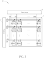
- FIG. 1 illustrates a schematic diagram of a display panel 10 of an embodiment.
- FIG. 2 illustrates a circuit diagram of the display panel 10.
- the display panel 10 includes a pixel circuit matrix 1, a vertical driver (V-driver) 2 and a data driver 3.
- the pixel circuit matrix 1 includes a plurality of pixels P11-PNM, which are located in regions where a plurality of scan lines S1-SN and a plurality of emission control lines E1-EN intersect a plurality of data lines D1-DM.
- the pixel circuit matrix 1 displays an image according to an applied data voltage.
- the vertical driver 2 may generate scan signals and emission control signals. In some embodiments, the vertical driver 2 may also generate compensation signals.
- the vertical driver 2 sequentially supplies scan signals to scan lines S1-SN in response to scan control signals (i.e., a start pulse and a clock signal).
- the vertical driver 2 also supplies emission control signals to emission control lines E1-EN in response to a start pulse and a clock signal output.
- the data driver 3 supplies data voltages corresponding to RGB (red, green, and blue) data to data lines D1-DM in response to data control signals.
- Each of the pixels P11-PNM includes R, G, and B pixel circuits.
- the R, G, and B pixel circuits have the same circuit construction and emit R, G, and B light with brightness corresponding to current supplied to pixel circuit.
- each of the pixels P11-PNM combines light emitted from the R, G, and B pixel circuits and displays a specific color according to the combination of pixel color and brightness.
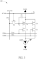
- FIG. 3 illustrates a diagram of a pixel circuit 100 of an embodiment.
- the pixel circuit 100 may be a pixel circuit Pnm (1 ⁇ m ⁇ M, 1 ⁇ n ⁇ N) in one of the pixels P11-PNM, with some variations.
- the pixel circuit 100 includes a switching transistor T2, a driving transistor T1a, a driving transistor T1b, an emission control transistor T3a, an emission control transistor T3b, a capacitor C1, and a light emitting diode LED1.
- the switching transistor T2, the driving transistors T1a and T1b, and the emission control transistors T3a and T3b each includes a first terminal, a second terminal and a control terminal.
- the control terminals of the driving transistor T1a and the driving transistor T1b are both coupled to the second terminal of the switching transistor T2.
- the second terminal of the driving transistor T1a can be coupled to the first terminal of the emission control transistor T3a.
- the second terminal of the driving transistor T1b can be coupled to the first terminal of the emission control transistor T3b.
- the light emitting diode LED1 can be coupled to the second terminal of the emission control transistors T3a and the second terminal of the emission control transistor T3b.
- the capacitor C1 can be coupled between the control terminal of the driving transistor T1a and the voltage source PVDD (i.e., DC voltage).
- the control terminal of the switching transistor T2 can be coupled to a scan line Sn.
- the first terminal of the switching transistor T2 can be coupled to a data line Dm.
- the control terminal of the emission control transistor T3a can be coupled to an emission control line EAn, and the control terminal of the emission control transistor T3b can be coupled to another emission control line EBn.
- the scan line Sn provides a scan signal SCANn to turn on the switching transistor T2 so that the data line Dm writes the data signal DATAm to the control terminals of the driving transistors T1a and T1b.
- the driving current is controlled by the driving transistors T1a and T1b according to the data signal DATAm input through the switching transistor T2.
- the capacitor C1 can store the charges for turning on the driving transistors T1a and T1b.
- the voltage PVDD is provided to the first terminal of the driving transistor T1a and the first terminal of the driving transistor T1b, and the voltage PVSS is provided to the light-emitting diode LED1.
- a voltage difference of the pixel circuit 100 can be established to enable driving current to flow from the terminal of the voltage PVDD to the terminal of the voltage PVSS, where the voltage PVDD is greater than the voltage PVSS.
- the emission control line EAn provides an emission control signal EMAn having a first duty cycle to the emission control transistor T3a.
- the emission control line EBn provides an emission control signal EMBn having a second duty cycle to the emission control transistor T3b.
- the first duty cycle may be different from the second duty cycle, and in some other embodiments, the first duty cycle may be the same as the second duty cycle.
- the light emission period of the light-emitting diode LED1 is controlled by emission control transistors T3a and T3b according to emission control signals EMAn and EMBn respectively. In some other embodiments, only one of the emission control signals EMAn and EMBn turns on the emission control switch with specific duty cycle.
- the switching transistor T2, the driving transistors T1a and T1b and the emission control transistors T3a and T3b can be p-type transistors.
- the driving transistor T1a and the driving transistor T1b have different channel width-to-length (W/L) ratios.
- the driving transistor T1a can be a low temperature poly-silicon (LTPS) thin-film transistor.
- the driving transistor T1b can be an oxide thin-film transistor.
- a driving unit includes the driving transistors T1a and T1b and the emission control transistors T3a and T3b coupled respectively in series.
- the emission control transistors T3a and T3b are commonly coupled to the light emitting diode LED1.
- the control terminals of emission control transistors T3a and T3b are controlled independently by the emission control signals EMAn and EMBn respectively to select suitable driving current according to either the high brightness mode or the low brightness mode.
- the scan signal SCANn, and emission control signals EMAn and EMBn can be provided by the vertical driver 2.
- the data signal DATAm can be provided by the data driver 3.
- the gate voltage Vg is set to the data voltage for a following display frame cycle such that the gate-source voltages (Vgs) of the driving transistor T1a and the driving transistor T1b are updated to generate the current for the following display frame cycle.
- the emission control transistor T3a is turned on by the emission control signal EMAn, then a large current would flow through the light emitting diode LED1 for the high brightness mode.
- the emission control transistor T3b is turned on by the emission control signal EMBn, then a small current would flow through the light emitting diode LED1 for the low brightness mode.
- more brightness modes can be created by adding more driving transistors and emission control transistors respectively constructed by the same principle to the pixel circuit.
- the disclosure is not limited thereto.
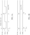
- FIG. 4A illustrates a timing diagram of the operation signals of the pixel circuit 100 of an embodiment according to the high brightness mode.
- the scan signal SCANn, the emission control signals EMAn and EMBn are at high levels.
- the initial states of the driving transistors T1a and T1b, the switching transistor T2, and the emission control transistors T3a and T3b are turned off.
- a display frame cycle starts at time t1.
- a low pulse occurs in the scan signal SCANn, allowing the data signal DATAm to pass through the switching transistor T2 to control the driving transistors T1a and T1b.
- a low pulse occurs in the emission control signal EMAn to turn on the emission control transistor T3a.
- the emission control signal EMBn is maintained at the high level to keep the emission control transistor T3b turned off.
- a large driving current can flow from the terminal of the voltage PVDD to the terminal of the voltage PVSS for a longer period to drive the light emitting diode LED1 for the high brightness mode display.
- another display frame cycle begins. The behavior of the operation signals is similar for the various display frame cycles and the description is not repeated herein for brevity.
- FIG. 4B illustrates a timing diagram of the operation signals of the pixel circuit 100 of an embodiment according to the low brightness mode.
- the scan signal SCANn, the emission control signals EMAn and EMBn are at high levels.
- the initial states of the driving transistors T1a and T1b, the switching transistor T2, and the emission control transistors T3a and T3b are turned off.
- a display frame cycle starts at time 11. Between time t1 and t2, a low pulse occurs in the scan signal SCANn, allowing the data signal DATAm to pass through the switching transistor T2 to control the driving transistors T1a and T1b.
- a low pulse occurs in the emission control signal EMBn to turn on the emission control transistor T3b.
- the emission control signal EMAn is maintained at the high level to keep the emission control transistor T3a turned off.
- a small driving current can flow from the terminal of the voltage PVDD to the terminal of the voltage PVSS for a shorter period to drive the light emitting diode LED1 for the low brightness mode display.
- another display frame cycle begins. The behavior of the operation signals is similar for the various display frame cycles and the description is not repeated herein for brevity.
- FIG. 5 illustrates a diagram of a pixel circuit 200 of another embodiment.
- the pixel circuit 200 may be a pixel circuit Pnm in one of the pixels P11-PNM, with some variations.
- the pixel circuit 200 includes a switching transistor T2, a driving transistor T1a, a driving transistor T1b, an emission control transistor T3a, an emission control transistor T3b, a capacitor C1, and a light emitting diode LED1.
- the switching transistor T2, the driving transistors T1a and T1b, the emission control transistor T3a and T3b each include a first terminal, a second terminal and a control terminal.
- the control terminals of the driving transistor T1a and the driving transistor T1b are both coupled to the second terminal of the switching transistor T2.
- the first terminal of the driving transistor T1a can be coupled to the second terminal of the emission control transistor T3a.
- the first terminal of the driving transistor T1b can be coupled to the second terminal of the emission control transistor T3b.
- the light emitting diode LED1 can be coupled to the first terminal of the emission control transistor T3a and the first terminal of the emission control transistor T3b.
- the capacitor C1 can be coupled between the control terminal of the driving transistor T1a and the voltage source PVSS.
- the control terminal of the switching transistor T2 can be coupled to a scan line Sn.
- the first terminal of the switching transistor T2 can be coupled to a data line Dm.
- the control terminal of the emission control transistor T3a can be coupled to an emission control line EAn, and the control terminal of the emission control transistor T3b can be coupled to another emission control line EBn.
- the scan line Sn provides a scan signal SCANn to the switching transistor T2 so that the data line Dm writes the data signal DATAm to the control terminals of the driving transistors T1a and T1b.
- the driving current is controlled by the driving transistors T1a and T1b according to the data signal DATAm input through the switching transistor T2.
- the voltage PVSS is provided to the first terminal of the driving transistor T1a and the first terminal of the driving transistor T1b, and the voltage PVDD is provided to the light-emitting diode LED1.
- a voltage difference of the pixel circuit 200 can be established to enable driving current to flow from the terminal of the voltage PVDD to the terminal of the voltage PVSS, where the voltage PVDD is greater than the voltage PVSS.
- the emission control line EAn provides an emission control signal EMAn having a first duty cycle to the emission control transistor T3a.
- the emission control line EBn provides an emission control signal EMBn having a second duty cycle to the emission control transistor T3b.
- the first duty cycle may be different from the second duty cycle, and in some other embodiments, the first duty cycle may be the same as the second duty cycle.
- the light emission period of the light-emitting diode LED1 is controlled by emission control transistors T3a and T3b according to emission control signals EMAn and EMBn respectively.
- the switching transistor T2, the driving transistors T1a and T1b and the emission control transistors T3a and T3b can be n-type transistors.
- the driving transistor T1a and the driving transistor T1b have different channel width-to-length (W/L) ratios.
- the driving transistor T1a can be a low temperature poly-silicon (LTPS) thin-film transistor.
- the driving transistor T1b can be an oxide thin-film transistor.
- a driving unit includes the driving transistors T1a and T1b and the emission control transistors T3a and T3b coupled respectively in series.
- the emission control transistors T3a and T3b are commonly coupled to the light emitting diode LED1.
- the control terminals of emission control transistors T3a and T3b are controlled independently by the emission control signals EMAn and EMBn respectively to select suitable driving current according to either the high brightness mode or the low brightness mode.
- the scan signal SCANn, and the emission control signals EMAn and EMBn can be provided by the vertical driver 2.
- the data signal DATAm can be provided by the data driver 3.
- the gate voltage Vg is set to the data voltage of a following display frame cycle such that the gate-source voltages (Vgs) of the driving transistor T1a and the driving transistor T1b are updated to generate the current for the following display frame cycle.
- the emission control transistor T3a is turned on by the emission control signal EMAn, then a large current would flow through the light emitting diode LED for the high brightness mode.
- the emission control transistor T3b is turned on by the emission control signal EMBn, then a small current would flow through the light emitting diode LED for the low brightness mode.
- the operation signals of the pixel circuit 200 are similar to those of the pixel circuit 100 thus the description is not be repeated herein for brevity.
- more brightness modes can be created by adding more driving transistors and emission control transistors respectively constructed by the same principle to the pixel circuit.
- the disclosure is not limited thereto.
- FIG. 6 illustrates a diagram of a pixel circuit 300 of another embodiment.
- the pixel circuit 300 may be a pixel circuit Pnm (1 ⁇ m ⁇ M, 1 ⁇ n ⁇ N) in one of the pixels P11-PNM, with some variations.
- the pixel circuit 300 includes a switching transistor T2, a driving transistor T1a, a driving transistor T1b, an emission control transistor T3a, an emission control transistor T3b, a capacitor C1, and a light emitting diode LED1.
- the switching transistor T2, the driving transistors T1a and T1b, the emission control transistor T3a and T3b each include a first terminal, a second terminal and a control terminal.
- the control terminals of the driving transistor T1a and the driving transistor T1b are both coupled to the second terminal of the switching transistor T2.
- the second terminal of the emission control transistor T3a can be coupled to the first terminal of the driving transistor T1a.
- the second terminal of the emission control transistor T3b can be coupled to the first terminal of the driving transistor T1b.
- the light emitting diode LED1 can be coupled to the second terminal of the driving transistor T1a and the second terminal of the driving transistor T1b.
- the capacitor C1 can be coupled between the control terminal of the driving transistor T1a and the voltage source PVDD (i.e., a DC voltage).
- the control terminal of the switching transistor T2 can be coupled to a scan line Sn.
- the first terminal of the switching transistor T2 can be coupled to a data line Dm.
- the control terminal of the emission control transistor T3a can be coupled to an emission control line EAn, and the control terminal of the emission control transistor T3b can be coupled to another emission control line EBn.
- the scan line Sn provides a scan signal SCANn to the switching transistor T2 to w so that the data line Dm writes the data signal DATAm to the control terminals of the driving transistors T1a and T1b.
- the driving current is controlled by the driving transistors T1a and T1b according to the data signal DATAm input through the switching transistor T2.
- the voltage PVDD is provided to the first terminal of the emission control transistor T3a and the first terminal of the emission control transistor T3b, and the voltage PVSS is provided to the light-emitting diode LED1.
- a voltage difference of the pixel circuit 300 can be established to enable driving current to flow from the terminal of the voltage PVDD to the terminal of the voltage PVSS, where the voltage PVDD is greater than the voltage PVSS.
- the emission control line EAn provides an emission control signal EMAn having a first duty cycle to the emission control transistor T3a.
- the emission control line EBn provides an emission control signal EMBn having a second duty cycle to the emission control transistor T3b.
- the first duty cycle may be different from the second duty cycle, and in some other embodiments, the first duty cycle may be the same as the second duty cycle.
- the light emission period of the light-emitting diode LED1 is controlled by emission control transistors T3a and T3b according to emission control signals EMAn and EMBn respectively.
- the switching transistor T2, the driving transistors T1a and T1b and the emission control transistors T3a and T3b can be p-type transistors.
- the driving transistor T1a and the driving transistor T1b have different channel width-to-length (W/L) ratios.
- the driving transistor T1a can be a low temperature poly-silicon (LTPS) thin-film transistor.
- the driving transistor T1b can be an oxide thin-film transistor.
- a driving unit includes the driving transistors T1a and T1b and the emission control transistors T3a and T3b coupled respectively in series.
- the driving transistors T1a and T1b are commonly coupled to the light emitting diode LED1.
- the control terminals of emission control transistors T3a and T3b are controlled independently by the emission control signals EMAn and EMBn respectively to select suitable driving current according to either the high brightness mode or the low brightness mode.
- the scan signal SCANn, and emission control signals EMAn and EMBn can be provided by the vertical driver 2.
- the data signal DATAm can be provided by the data driver 3.
- the operation signals of the pixel circuit 300 are similar to those of the pixel circuit 100, thus the description is not be repeated herein for brevity.
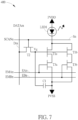
- FIG. 7 illustrates a diagram of a pixel circuit 400 of another embodiment.
- the pixel circuit 400 may be a pixel circuit Pnm (1 ⁇ m ⁇ M, 1 ⁇ n ⁇ N) in one of the pixels P11-PNM, with some variations.
- the pixel circuit 400 includes a switching transistor T2, a driving transistor T1a, a driving transistor T1b, an emission control transistor T3a, an emission control transistor T3b, a capacitor C1, and a light emitting diode LED1.
- the switching transistor T2, the driving transistors T1a and T1b, and the emission control transistor T3a and T3b each include a first terminal, a second terminal and a control terminal.
- the control terminals of the driving transistor T1a and the driving transistor T1b are both coupled to the second terminal of the switching transistor T2.
- the second terminal of the driving transistor T1a can be coupled to the first terminal of the emission control transistor T3a.
- the second terminal of the driving transistor T1b can be coupled to the first terminal of the emission control transistor T3b.
- the light emitting diode LED1 can be coupled to the first terminals of the driving transistors T1a and T1b.
- the capacitor C1 can be coupled between the control terminal of the driving transistor T1a and the voltage source PVSS.
- the control terminal of the switching transistor T2 can be coupled to a scan line Sn.
- the first terminal of the switching transistor T2 can be coupled to a data line Dm.
- the control terminal of the emission control transistor T3a can be coupled to an emission control line EAn, and the control terminal of the emission control transistor T3b can be coupled to another emission control line EBn.
- the scan line Sn provides a scan signal SCANn to the switching transistor T2 so that the data line Dm writes the data signal DATAm to the control terminals of the driving transistors T1a and T1b.
- the driving current is controlled by the driving transistors T1a and T1b according to the data signal DATAm input through the switching transistor T2.
- the voltage PVSS is provided to the second terminal of the emission control transistor T3a and the second terminal of the emission control transistor T3b, and the voltage PVDD is provided to the light-emitting diode LED1.
- a voltage difference of the pixel circuit 400 can be established to enable driving current to flow from the terminal of the voltage PVDD to the terminal of the voltage PVSS, where the voltage PVDD is greater than the voltage PVSS.
- the emission control line EAn provides an emission control signal EMAn having a first duty cycle to the emission control transistor T3a.
- the emission control line EBn provides an emission control signal EMBn having a second duty cycle to the emission control transistor T3b.
- the first duty cycle may be different from the second duty cycle, and in some other embodiments, the first duty cycle may be the same as the second duty cycle.
- the light emission period of the light-emitting diode LED1 is controlled by emission control transistors T3a and T3b according to the emission control signals EMAn and EMBn respectively.
- the switching transistor T2, the driving transistors T1a and T1b and the emission control transistors T3a and T3b can be n-type transistors.
- the driving transistor T1a and the driving transistor T1b have different channel width-to-length (W/L) ratios.
- the driving transistor T1a can be a low temperature poly-silicon (LTPS) thin-film transistor.
- the driving transistor T1b can be an oxide thin-film transistor.
- a driving unit includes the driving transistors T1a and T1b and the emission control transistors T3a and T3b coupled respectively in series.
- the driving transistors T1a and T1b are commonly coupled to the light emitting diode LED1.
- the control terminals of emission control transistors T3a and T3b are controlled independently by the emission control signals EMAn and EMBn respectively to select suitable driving current according to either the high brightness mode or the low brightness mode.
- the scan signal SCANn, and the emission control signals EMAn and EMBn can be provided by the vertical driver 2.
- the data signal DATAm can be provided by the data driver 3.
- the operation signals of the pixel circuit 400 are similar to those of the pixel circuit 100, thus the description is not be repeated herein for brevity.
- FIG. 8 illustrates a diagram of a pixel circuit 500 of another embodiment.
- the pixel circuit 500 may be a pixel circuit Pnm (1 ⁇ m ⁇ M, 1 ⁇ n ⁇ N) in one of the pixels P11-PNM, with some variations.
- the pixel circuit 500 includes a switching transistor T2, driving transistors T1a and T1b, emission control transistors T3a, T3b, T6a and T6b, reset transistors T4aand T4b, compensation transistors T5a and T5b, capacitors C1a and C1b, and a light emitting diode LED1.
- the switching transistor T2, the driving transistors T1a and T1b, the emission control transistor T3a, T3b, T6a and T6b, and the reset transistors T4a and T4b, compensation transistors T5a and T5b each include a first terminal, a second terminal and a control terminal.
- the control terminal of the driving transistor T1a can be coupled to the second terminal of the reset transistor T4a.
- the control terminal of the driving transistor T1b can be coupled to the second terminal of the reset transistor T4b.
- the second terminal of the driving transistor T1a can be coupled to the first terminal of the emission control transistor T3a.
- the second terminal of the driving transistor T1b can be coupled to the first terminal of the emission control transistor T3b.
- the light emitting diode LED1 can be coupled to the second terminal of the emission control transistor T3a and the second terminal of the emission control transistor T3b.
- the control terminals of the reset transistors T4a and T4b are both coupled to a reset line Rn.
- the control terminals of the compensation transistors T5a and T5b are both coupled to the scan line Sn.
- the capacitor C1a can be coupled between the control terminal of the driving transistor T1a and the voltage source PVDD.
- the capacitor C1b can be coupled between the control terminal of the driving transistor T1b and the voltage source PVDD.
- the second terminal of the compensation transistor T5a can be coupled to the control terminal of the driving transistor T1a, and the first terminal of the compensation transistor T5a can be coupled to the second terminal of the driving transistor T1a.
- the second terminal of the compensation transistor T5b can be coupled to the control terminal of the driving transistor T1b, and the first terminal of the compensation transistor T5b can be coupled to the second terminal of the driving transistor T1b.
- the control terminal of the switching transistor T2 can be coupled to a scan line Sn.
- the first terminal of the switching transistor T2 can be coupled to a data line Dm.
- the second terminal of the switching transistor T2 can be coupled to the first terminals of driving transistors T1a and T1b.
- the control terminals of the emission control transistor T3a and T6a can be coupled to an emission control line EAn, and the control terminals of the emission control transistor T3b and T6b can be coupled to another emission control line EBn.
- the second terminals of the emission control transistors T6a and T6b are coupled to the first terminals of the driving transistors T1a and T1b respectively.
- the scan line Sn provides a scan signal SCANn to the switching transistor T2 and compensation transistors T5a and T5b so that the data line Dm writes the data signal DATAm to the control terminals of the driving transistors T1a and T1b.
- the driving current is controlled by the driving transistors T1a and T1b according to the data signal DATAm input through the switching transistor T2.
- the capacitors C1a and C1b can store the charges for turning on the driving transistors T1a and T1b respectively.
- the voltage PVDD is provided to the first terminal of the driving transistor T6a and the first terminal of the driving transistor T6b, and the voltage PVSS is provided to the light-emitting diode LED 1.
- a voltage difference of the pixel circuit 500 can be established to enable driving current to flow from the terminal of the voltage PVDD to the terminal of the voltage PVSS, where the voltage PVDD is greater than the voltage PVSS.
- the reset line Rn provides a reset signal RSTn to the reset transistors T4a and T4b.
- a voltage VRST is provided to the first terminals of the reset transistors T4a and T4b. They function to set the driving transistors T1a and T1b to receive the data signal DATAm for a following display frame cycle.
- the emission control line EAn provides an emission control signal EMAn having a first duty cycle to the emission control transistors T3a and T6a.
- the emission control line EBn provides an emission control signal EMBn having a second duty cycle to the emission control transistors T3b and T6b.
- the first duty cycle may be different from the second duty cycle, and in some other embodiments, the first duty cycle may be the same as the second duty cycle.
- the light emission period of the light-emitting diode LED1 is controlled by emission control transistors T3a, T6a and T3b, T6b according to the emission control signals EMAn and EMBn respectively.
- the switching transistor T2, the driving transistors T1a and T1b, the emission control transistor T3a, T3b, T6a and T6b, the reset transistors T4aand T4b, compensation transistors T5a and T5b, can be p-type transistors.
- the driving transistor T1a and the driving transistor T1b have different channel width-to-length (W/L) ratios.
- the driving transistor T1a can be a low temperature poly-silicon (LTPS) thin-film transistor.
- the driving transistor T1b can be an oxide thin-film transistor.
- FIG. 9A illustrates a timing diagram of the operation signals of the pixel circuit 500 of an embodiment according to the high brightness mode.
- the reset signal RSTn the scan signal SCANn
- the emission control signals EMAn and EMBn are at high levels.
- the initial states of the switching transistor T2 the emission control transistors T3a, T3b, T6a and T6b, and the reset transistors T4aand T4b, compensation transistors T5a and T5b are turned off.
- a low pulse occurs in the reset signal RSTn to turn on the reset transistors T4a and T4b allowing the voltage VRST to reset the driving transistors T1a and T1b.
- This mechanism ensures that the driving transistors T1a and T1b can be turned on during the following display frame cycle.
- the display frame cycle starts at time t2.
- a low pulse occurs in the scan signal SCANn, allowing the data signal DATAm to pass through the switching transistor T2 to the respective first terminals of the driving transistors T1a and T1b.
- the data signal DATAm can be transferred through the respective compensation transistors T5a and T5b to the respective control terminals of the driving transistors T1a and T1b, thus the control voltage of the driving transistors T1a and T1b are determined.
- a low pulse occurs in the emission control signal EMAn to turn on the emission control transistors T3a and T6a.
- the emission control signal EMBn is maintained at the high level to keep the emission control transistors T3b and T6b turned off.
- a large driving current can flow from the terminal of the voltage PVDD to the terminal of the voltage PVSS to drive the light emitting diode LED1 for the high brightness mode display.
- another display frame cycle begins. The behavior of the operation signals is similar for the various display frame cycles and the description is not repeated herein for brevity.
- FIG. 9B illustrates a timing diagram of the operation signals of the pixel circuit 500 of an embodiment according to the low brightness mode.
- the reset signal RSTn, the scan signal SCANn, the emission control signals EMAn and EMBn are at high levels.
- the initial states of the switching transistor T2 the emission control transistors T3a, T3b, T6a and T6b, and the reset transistors T4a and T4b, compensation transistors T5a and T5b are turned off.
- a low pulse occurs in the reset signal RSTn to turn on the reset transistors T4a and T4b allowing the voltage VRST to reset the driving transistors T1a and T1b.
- This mechanism ensures that the driving transistors T1a and T1b can be turned on during the following display frame cycle.
- the display frame cycle starts at time t2. Between time t2 and t3, a low pulse occurs in the scan signal SCANn, allowing the data signal DATAm to pass through the switching transistor T2 to the respective first terminals of the driving transistors T1a and T1b. While the compensation transistors T5a and T5b are turned on, the data signal DATAm can be transferred through the respective compensation transistors T5a and T5b to the respective control terminals of the driving transistors T1a and T1b, thus the control voltage of the driving transistors T1a and T1b are determined.
- a low pulse occurs in the emission control signal EMBn to turn on the emission control transistors T3b and T6b.
- the emission control signal EMAn is maintained at the high level to keep the emission control transistors T3a and T6a turned off.
- a small driving current can flow from the terminal of the voltage PVDD to the terminal of the voltage PVSS to drive the light emitting diode LED1 for the low brightness mode display.
- another display frame cycle begins.
- the behavior of the operation signals is similar for the various display frame cycles and the description is not repeated herein for brevity.
- FIG. 10 illustrates a diagram of a pixel circuit 600 of another embodiment.
- the pixel circuit 600 may be a pixel circuit Pnm (1 ⁇ m ⁇ M, 1 ⁇ n ⁇ N) in one of the pixels P11-PNM, with some variations.
- the pixel circuit 600 includes a switching transistor T2, driving transistors T1a and T1b, emission control transistors T3a, T3b, T6a and T6b, reset transistor T4, compensation transistors T5a and T5b, capacitors C1, and a light emitting diode LED1.
- the switching transistor T2, the driving transistors T1a and T1b, the emission control transistor T3a, T3b, T6a and T6b, the reset transistors T4, and the compensation transistors T5a and T5b each include a first terminal, a second terminal and a control terminal.
- the control terminal of the driving transistor T1a can be coupled to the second terminal of the reset transistor T4.
- the control terminal of the driving transistor T1b can be coupled to the second terminal of the reset transistor T4.
- the first terminal of the emission control transistor T3a can be coupled to the second terminal of the driving transistor T1a.
- the first terminal of the emission control transistor T3b can be coupled to the second terminal of the driving transistor T1b.
- the light emitting diode LED1 can be coupled to the second terminal of the emission control transistors T3a and the second terminal of the emission control transistor T3b.
- the control terminal of the reset transistor T4 can be coupled to a reset line Rn.
- the control terminal of the compensation transistor T5a can be coupled to a compensation line CAn, and the control terminal of the compensation transistor T5b can be coupled to another compensation line CBn.
- the capacitor C1 can be coupled between the control terminal of the driving transistor T1a and the voltage source PVDD.
- the second terminal of the compensation transistor T5a can be coupled to the control terminal of the driving transistor T1a, and the first terminal of the compensation transistor T5a can be coupled to the second terminal of the driving transistor T1a.
- the second terminal of the compensation transistor T5b can be coupled to the control terminal of the driving transistor T1b, and the second terminal of the compensation transistor T5b can be coupled to the second terminal of the driving transistor T1b.
- the control terminal of the switching transistor T2 can be coupled to a scan line Sn.
- the first terminal of the switching transistor T2 can be coupled to a data line Dm.
- the second terminal of the switching transistor T2 can be coupled to the first terminals of driving transistors T1a and T1b.
- the control terminals of the emission control transistors T3a and T6a can be coupled to an emission control line EAn, and the control terminals of the emission control transistors T3b and T6b can be coupled to another emission control line EBn.
- the second terminals of the emission control transistors T6a and T6b are coupled to the first terminals of the driving transistors T1a and T1b respectively.
- the scan line Sn provides a scan signal SCANn to the switching transistor T2 and compensation transistors T5a and T5b so that the data line Dm writes the data signal DATAm to the control terminals of the driving transistors T1a and T1b.
- the driving current is controlled by the driving transistors T1a and T1b according to the data signal DATAm input through the switching transistor T2.
- the voltage PVDD is provided to the first terminal of the driving transistor T6a and the first terminal of the driving transistor T6b, and the voltage PVSS is provided to the light-emitting diode LED1.
- a voltage difference of the pixel circuit 600 can be established to enable driving current to flow from the terminal of the voltage PVDD to the terminal of the voltage PVSS, where the voltage PVDD is greater than the voltage PVSS.
- the reset line Rn provides a reset signal RSTn to the reset transistor T4.
- a voltage VRST is provided to the first terminal of the reset transistor T4.
- the reset transistor T4 functions to set the driving transistors T1a and T1b to receive the data signal DATAm for a following display frame cycle.
- the compensation lines CAn and CBn provide respectively the compensation signals CPAn and CPBn to independently control the compensation transistors T5a and T5b.
- the emission control line EAn provides an emission control signal EMAn having a first duty cycle to the emission control transistors T3a and T6a.
- the emission control line EBn provides an emission control signal EMBn having a second duty cycle to the emission control transistors T3b and T6b.
- the first duty cycle may be different from the second duty cycle, and in some other embodiments, the first duty cycle may be the same as the second duty cycle.
- the light emission period of the light-emitting diode LED1 is controlled by emission control transistors T3a, T6a and T3b, T6b according to the emission control signals EMAn and EMBn respectively.
- the scan signal SCANn, the compensation signals CPAn and CPBn, and the emission control signals EMAn and EMBn can be provided by the vertical driver 2.
- the data signal DATAm can be provided by the data driver 3.
- the switching transistor T2, the driving transistors T1a and T1b, the emission control transistor T3a, T3b, T6a and T6b, the reset transistor T4, compensation transistors T5a and T5b, can be p-type transistors.
- the driving transistor T1a and the driving transistor T1b have different channel width-to-length (W/L) ratios.
- the driving transistor T1a can be a low temperature poly-silicon (LTPS) thin-film transistor.
- the driving transistor T1b can be an oxide thin-film transistor.
- FIG. 11A illustrates a timing diagram of the operation signals of the pixel circuit 600 of an embodiment according to the high brightness mode.
- the reset signal RSTn the scan signal SCANn
- the emission control signals EMAn and EMBn the compensation signals CPAn and CPBn are at high levels.
- the initial states of the switching transistor T2 the emission control transistors T3a, T3b, T6a and T6b, and the reset transistor T4
- compensation transistors T5a and T5b are turned off.
- a low pulse occurs in the reset signal RSTn to turn on the reset transistors T4 allowing the voltage VRST to reset the driving transistors T1a and T1b.
- This mechanism ensures that the driving transistors T1a and T1b can be turned on during the following display frame cycle.
- the display frame cycle starts at time t2.
- a low pulse occurs in the scan signal SCANn, allowing the data signal DATAm to pass through the switching transistor T2 to the respective first terminals of the driving transistors T1a and T1b.
- a low pulse occurs in the compensation signal CPAn to turn on the compensation transistor T5a.
- the compensation transistor T5a While the compensation transistor T5a is turned on, the data signal DATAm can be transferred through the compensation transistor T5a to the control terminal of the driving transistors T1a, thus the control voltage of the driving transistor T1a is determined.
- the compensation signal CPBn is maintained at the high level.
- a low pulse occurs in the emission control signal EMAn to turn on the emission control transistors T3a and T6a.
- the emission control signal EMBn is maintained at the high level to keep the emission control transistors T3b and T6b turned off.
- a large driving current can flow from the terminal of the voltage PVDD to the terminal of the voltage PVSS to drive the light emitting diode LED1 for the high brightness mode display.
- another display frame cycle begins.
- the behavior of the operation signals is similar for the various display frame cycles and the description is not repeated herein for brevity.
- FIG. 11B illustrates a timing diagram of the operation signals of the pixel circuit 600 of an embodiment according to the low brightness mode.
- the reset signal RSTn, the scan signal SCANn, the emission control signals EMAn and EMBn, the compensation signals CPAn and CPBn are at high levels.
- the initial states of the switching transistor T2 the emission control transistors T3a, T3b, T6a and T6b, and the reset transistor T4, compensation transistors T5a and T5b are turned off.
- a low pulse occurs in the reset signal RSTn to turn on the reset transistor T4 allowing the voltage VRST to reset the driving transistors T1a and T1b.
- This mechanism ensures that the driving transistors T1a and T1b can be turned on during the following display frame cycle.
- the display frame cycle starts at time t2. Between time t2 and t3, a low pulse occurs in the scan signal SCANn, allowing the data signal DATAm to pass through the switching transistor T2 to the respective first terminals of the driving transistors T1a and T1b. At the same time, a low pulse occurs in the compensation signal CPBn to turn on the compensation transistor T5b. While the compensation transistor T5b is turned on, the data signal DATAm can be transferred through the compensation transistor T5b to the control terminal of the driving transistors T1b, thus the control voltage of the driving transistor T1b is determined. The compensation signal CPAn is maintained at the high level.
- a low pulse occurs in the emission control signal EMBn to turn on the emission control transistors T3b and T6b.
- the emission control signal EMAn is maintained at the high level to keep the emission control transistors T3a and T6a turned off.
- a small driving current can flow from the terminal of the voltage PVDD to the terminal of the voltage PVSS to drive the light emitting diode LED1 for the low brightness mode display.
- another display frame cycle begins.
- the behavior of the operation signals is similar for the various display frame cycles and the description is not repeated herein for brevity.
- FIG. 12 illustrates a diagram of a pixel circuit 700 of another embodiment.
- the pixel circuit 700 may be a pixel circuit Pnm (1 ⁇ m ⁇ M, 1 ⁇ n ⁇ N) in one of the pixels P11-PNM, with some variations.
- the pixel circuit 700 includes a switching transistor T2, driving transistors T1a and T1b, emission control transistors T3a and T3b, reset transistors T4a and T4b, compensation transistors T5a and T5b, reference control transistor T7, capacitors C1a, C1b, C2a and C2b, and a light emitting diode LED1.
- the switching transistor T2, the driving transistors T1a and T1b, the emission control transistor T3a and T3b, the reset transistors T4a and T4b, compensation transistors T5a and T5b, and the reference control transistor T7 each include a first terminal, a second terminal and a control terminal.
- the control terminal of the driving transistor T1a can be coupled to the second terminal of the reset transistor T4a.
- the control terminal of the driving transistor T1b can be coupled to the second terminal of the reset transistor T4b.
- the second terminal of the driving transistor T1a can be coupled to the first terminal of the emission control transistor T3a.
- the second terminal of the driving transistor T1b can be coupled to the first terminal of the emission control transistor T3b.
- the light emitting diode LED1 can be coupled to the second terminal of the emission control transistor T3a and the second terminal of the emission control transistor T3b.
- the control terminals of the reset transistors T4a and T4b are both coupled to a reset line Rn.
- the control terminals of the compensation transistors T5a and T5b are both coupled to the scan line Sn.
- the capacitor C1a can be coupled between the control terminal of the driving transistor T1a and the voltage source PVDD.
- the capacitor C1b can be coupled between the control terminal of the driving transistor T1b and the voltage source PVDD.
- the capacitor C2a can be coupled between the second terminal of the switching transistor T2 and the control terminal of the driving transistor T1a.
- the capacitor C2b can be coupled between the second terminal of the switching transistor T2 and the control terminal of the driving transistor T1b.
- the second terminal of the compensation transistor T5a can be coupled to the control terminal of the driving transistor T1a, and the first terminal of the compensation transistor T5a can be coupled to the second terminal of the driving transistor T1a.
- the second terminal of the compensation transistor T5b can be coupled to the control terminal of the driving transistor T1b, and the first terminal of the compensation transistor T5b can be coupled to the second terminal of the driving transistor T1b.
- the control terminal of the switching transistor T2 can be coupled to a scan line Sn.
- the first terminal of the switching transistor T2 can be coupled to a data line Dm.
- the control terminal of the emission control transistor T3a can be coupled to an emission control line EAn, and the control terminal of the emission control transistor T3b can be coupled to another emission control line EBn.
- the control terminal of the reference control transistor T7 can be coupled to the scan line Sn.
- the second terminal of the reference control transistor T7 can be coupled to the second terminal of the switching transistor T2.
- the scan line Sn provides a scan signal SCANn to the switching transistor T2, compensation transistors T5a and T5b and the reference control transistor T7 so that the data line Dm writes the data signal DATAm to the control terminals of the driving transistors T1a and T1b.
- the voltage VREF is provided to the first terminal the reference control transistor T7 to provide a coupling voltage for the capacitors C2a and C2b.
- the driving current is controlled by the driving transistors T1a and T1b according to the data signal DATAm with capacitive coupling of the capacitor C2a and C2b respectively.
- the capacitors C2a and C2b can be used to drive the driving transistors T1a and T1b respectively.
- the voltage PVDD is provided to the first terminal of the driving transistor T1a and the first terminal of the driving transistor T1b, and the voltage PVSS is provided to the light-emitting diode LED1.
- a voltage difference of the pixel circuit 700 can be established to enable driving current to flow from the terminal of the voltage PVDD to the terminal of the voltage PVSS, where the voltage PVDD is greater than the voltage PVSS.
- the reset line Rn provides a reset signal RSTn to the reset transistors T4a and T4b.
- a voltage VRST is provided to the first terminals of the reset transistors T4a and T4b. They function to set the driving transistors T1a and T1b to receive the data signal DATAm for a following display frame cycle.
- the emission control line EAn provides an emission control signal EMAn having a first duty cycle to the emission control transistor T3a.
- the emission control line EBn provides an emission control signal EMBn having a second duty cycle to the emission control transistor T3b.
- the first duty cycle may be different from the second duty cycle, and in some other embodiments, the first duty cycle may be the same as the second duty cycle.
- the light emission period of the light-emitting diode LED1 is controlled by emission control transistors T3a and T3b according to the emission control signals EMAn and EMBn respectively.
- the switching transistor T2, the driving transistors T1a and T1b, the emission control transistor T3a and T3b, and the reset transistors T4aand T4b, compensation transistors T5a and T5b, can be p-type transistors.
- the reference control transistor T7 can be an n-type transistor.
- the driving transistor T1a and the driving transistor T1b have different channel width-to-length (W/L) ratios.
- the driving transistor T1a can be a low temperature poly-silicon (LTPS) thin-film transistor.
- the driving transistor T1b can be an oxide thin-film transistor.
- FIG. 13A illustrates a timing diagram of the operation signals of the pixel circuit 700 of an embodiment according to the high brightness mode.
- the reset signal RSTn the scan signal SCANn
- the emission control signals EMAn and EMBn are at high levels.
- the initial states of the switching transistor T2 the emission control transistors T3a and T3b, and the reset transistors T4a and T4b, compensation transistors T5a and T5b, and the reference control transistor T7 are turned off.
- a low pulse occurs in the reset signal RSTn to turn on the reset transistors T4a and T4b allowing the voltage VRST to reset the driving transistors T1a and T1b.
- This mechanism ensures that the driving transistors T1a and T1b can be turned on during the following display frame cycle.
- the display frame cycle starts at time t2.
- a low pulse occurs in the scan signal SCANn to turn on the switching transistor T2, the reference transistor T7 and the compensation transistors T5a and T5b, allowing the data signal DATAm to pass through the switching transistor T2 and coupled to the respective capacitors C2a and C2b, thus controlling the driving transistors T1a and T1b.
- a low pulse occurs in the emission control signal EMAn to turn on the emission control transistors T3a.
- the emission control signal EMBn is maintained at the high level to keep the emission control transistor T3b turned off.
- a large driving current can flow from the terminal of the voltage PVDD to the terminal of the voltage PVSS to drive the light emitting diode LED1 for the high brightness mode display.
- another display frame cycle begins. The behavior of the operation signals is similar for the various display frame cycles and the description is not repeated herein for brevity.
- FIG. 13B illustrates a timing diagram of the operation signals of the pixel circuit 700 of an embodiment according to the low brightness mode.
- the reset signal RSTn, the scan signal SCANn, the emission control signals EMAn and EMBn are at high levels.
- the initial states of the switching transistor T2 the emission control transistors T3a and T3b, and the reset transistors T4a and T4b, compensation transistors T5a and T5b, and the reference control transistor T7 are turned off.
- a low pulse occurs in the reset signal RSTn to turn on the reset transistors T4a and T4b allowing the voltage VRST to reset the driving transistors T1a and T1b.
- This mechanism ensures that the driving transistors T1a and T1b can be turned on during the following display frame cycle.
- the display frame cycle starts at time t2.
- a low pulse occurs in the scan signal SCANn to turn on the switching transistor T2, the reference transistor T7 and the compensation transistor T5a and T5b, allowing the data signal DATAm to pass through the switching transistor T2 and coupled to the respective capacitors C2a and C2b, thus controlling the driving transistors T1a and T1b.
- a low pulse occurs in the emission control signal EMBn to turn on the emission control transistors T3b.
- the emission control signal EMAn is maintained at the high level to keep the emission control transistor T3a turned off.
- FIG. 14 illustrates a diagram of a pixel circuit 800 of another embodiment.
- the pixel circuit 800 may be a pixel circuit Pnm (1 ⁇ m ⁇ M, 1 ⁇ n ⁇ N) in one of the pixels P11-PNM, with some variations.
- the pixel circuit 800 includes a switching transistor T2, driving transistors T1a and T1b, emission control transistors T3a and T3b, reset transistor T4, compensation transistors T5a and T5b, a reference control transistor T7, capacitors C1, C2, and a light emitting diode LED1.
- the switching transistor T2, the driving transistors T1a and T1b, the emission control transistor T3a and T3b, the reset transistor T4, compensation transistors T5a and T5b, and the reference control transistor T7 each include a first terminal, a second terminal and a control terminal.
- the control terminals of the driving transistor T1a and T1b can be coupled to the second terminal of the reset transistor T4.
- the second terminal of the driving transistor T1a can be coupled to the first terminal of the emission control transistor T3a.
- the second terminal of the driving transistor T1b can be coupled to the first terminal of the emission control transistor T3b.
- the light emitting diode LED1 can be coupled to the second terminal of the emission control transistors T3a and the second terminal of the emission control transistor T3b.
- the control terminal of the reset transistor T4 can be coupled to a reset line Rn.
- the control terminal of the compensation transistor T5a can be coupled to a compensation line CAn, and the control terminal of the compensation transistor T5b can be coupled to another compensation line CBn.
- the capacitor C1 can be coupled between the control terminal of the driving transistor T1a and the voltage source PVDD.
- the capacitor C2 can be coupled between the second terminal of the switching transistor T2 and the control terminal of the driving transistor T1a.
- the second terminal of the compensation transistor T5a can be coupled to the control terminal of the driving transistor T1a, and the first terminal of the compensation transistor T5a can be coupled to the second terminal of the driving transistor T1a.
- the second terminal of the compensation transistor T5b can be coupled to the control terminal of the driving transistor T1b, and the first terminal of the compensation transistor T5b can be coupled to the second terminal of the driving transistor T1b.
- the control terminal of the switching transistor T2 can be coupled to a scan line Sn.
- the first terminal of the switching transistor T2 can be coupled to a data line Dm.
- the control terminal of the emission control transistor T3a can be coupled to an emission control line EAn, and the control terminal of the emission control transistor T3b can be coupled to another emission control line EBn.
- the control terminal of the reference control transistor T7 can be coupled to the scan line Sn.
- the second terminal of the reference control transistor T7 can be coupled to the second terminal of the switching transistor T2.
- the scan line Sn provides a scan signal SCANn to the switching transistor T2, and the reference control transistor T7 so that the data line Dm writes the data signal DATAm to the control terminals of the driving transistors T1a and T1b.
- the voltage VREF is provided to the first terminal the reference control transistor T7 to provide a coupling voltage for the capacitor C2.
- the driving current is controlled by the driving transistors T1a and T1b according to the data signal DATAm with capacitive coupling of the capacitor C2.
- the capacitor C2 can be used to drive the driving transistors T1a and T1b. With a higher level of the data signal DATAm, a higher driving current through the driving transistor T1a or T1b can be produced.
- the voltage PVDD is provided to the first terminal of the driving transistor T1a and the first terminal of the driving transistor T1b, and the voltage PVSS is provided to the light-emitting diode LED1.
- a voltage difference of the pixel circuit 800 can be established to enable driving current to flow from the terminal of the voltage PVDD to the terminal of the voltage PVSS, where the voltage PVDD is greater than the voltage PVSS.
- the reset line Rn provides a reset signal RSTn to the reset transistor T4.
- a voltage VRST is provided to the first terminal of the reset transistor T4.
- the reset transistor T4 functions to set the driving transistors T1a and T1b to receive the data signal DATAm for a following display frame cycle.
- the compensation lines CAn and CBn provide respectively the compensation signals CPAn and CPBn to independently control the compensation transistors T5a and T5b.
- the emission control line EAn provides an emission control signal EMAn having a first duty cycle to the emission control transistor T3a.
- the emission control line EBn provides an emission control signal EMBn having a second duty cycle to the emission control transistor T3b.
- the first duty cycle may be different from the second duty cycle, and in some other embodiments, the first duty cycle may be the same as the second duty cycle.
- the light emission period of the light-emitting diode LED1 is controlled by emission control transistors T3a and T3b according to the emission control signals EMAn and EMBn respectively.
- the switching transistor T2, the driving transistors T1a and T1b, the emission control transistors T3a and T3b, the reset transistor T4, compensation transistors T5a and T5b can be p-type transistors.
- the reference control transistor T7 can be an n-type transistor.
- the driving transistor T1a and the driving transistor T1b have different channel width-to-length (W/L) ratios.
- the driving transistor T1a can be a low temperature poly-silicon (LTPS) thin-film transistor.
- the driving transistor T1b can be an oxide thin-film transistor.
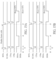
- FIG. 15A illustrates a timing diagram of the operation signals of the pixel circuit 800 of an embodiment according to the high brightness mode.
- the reset signal RSTn the scan signal SCANn
- the emission control signals EMAn and EMBn the emission control signals EMAn and EMBn
- the compensation signals CPAn and CPBn are at high levels.
- the initial states of the switching transistor T2, the emission control transistors T3a and T3b, and the reset transistor T4, compensation transistors T5a and T5b, and the reference control transistor T7 are turned off.
- a low pulse occurs in the reset signal RSTn to turn on the reset transistor T4 allowing the voltage VRST to reset the driving transistors T1a and T1b.
- This mechanism ensures that the driving transistors T1a and T1b can be turned on during the following display frame cycle.
- the display frame cycle starts at time t2.
- a low pulse occurs in the scan signal SCANn to turn on the switching transistor T2, and the reference transistor T7, allowing the data signal DATAm to pass through the switching transistor T2 and coupled to the capacitor C2, thus controlling the driving transistors T1a and T1b.
- a low pulse occurs in the compensation signal CPAn to turn on the compensation transistor T5a.
- the compensation signal CPBn is maintained at the high level.
- a low pulse occurs in the emission control signal EMAn to turn on the emission control transistor T3a.
- the emission control signal EMBn is maintained at the high level to keep the emission control transistor T3b turned off.
- a large driving current can flow from the terminal of the voltage PVDD to the terminal of the voltage PVSS to drive the light emitting diode LED1 for the high brightness mode display.
- another display frame cycle begins.
- the behavior of the operation signals is similar for the various display frame cycles and the description is not repeated herein for brevity.
- FIG. 15B illustrates a timing diagram of the operation signals of the pixel circuit 800 according to the low brightness mode of an embodiment.
- the reset signal RSTn the scan signal SCANn
- the emission control signals EMAn and EMBn the emission control signals EMAn and EMBn
- the compensation signals CPAn and CPBn are at high levels.
- the initial states of the driving transistors T1a and T1b, the switching transistor T2, the emission control transistors T3a and T3b, and the reset transistor T4, compensation transistors T5a and T5b, and the reference control transistor T7 are turned off.
- a low pulse occurs in the reset signal RSTn to turn on the reset transistor T4 allowing the voltage VRST to reset the driving transistors T1a and T1b.
- This mechanism ensures that the driving transistors T1a and T1b can be turned on during the following display frame cycle.
- the display frame cycle starts at time t2.
- a low pulse occurs in the scan signal SCANn to turn on the switching transistor T2, and the reference transistor T7, allowing the data signal DATAm to pass through the switching transistor T2 and coupled to the capacitor C2, thus controlling the driving transistors T1a and T1b.
- a low pulse occurs in the compensation signal CPBn to turn on the compensation transistor T5b.
- the compensation signal CPAn is maintained at the high level.
- a low pulse occurs in the emission control signal EMBn to turn on the emission control transistors T3b.
- the emission control signal EMAn is maintained at the high level to keep the emission control transistor T3a turned off.
- a small driving current can flow from the terminal of the voltage PVDD to the terminal of the voltage PVSS to drive the light emitting diode LED1 for the low brightness mode display.
- another display frame cycle begins.
- the behavior of the operation signals is similar for the various display frame cycles and the description is not repeated herein for brevity.
- control terminal of a transistor may be a gate; the first terminal of a transistor may be a source; the second terminal of a transistor may be a drain.
- the source and the drain may be reversed according to the implementation.
- FIG. 16 illustrates a brightness mode control system 20 of an embodiment.
- the brightness mode control system 20 may be coupled to the display panel 10 and includes an ambient light sensor 21, an illumination intensity comparator 22 coupled to the ambient light sensor 21, a display controller 23 coupled to the illumination intensity comparator 22.
- the display controller 23 has a timing controller 24, a display data processor 25 and a grayscale controller 26.
- the grayscale controller 26 has a high brightness mode LUT (look-up table) 27 and a low brightness mode LUT 28.
- the ambient light sensor 21 can detect an intensity of the ambient light.
- the illumination intensity comparator 22 can determine whether to enable the high brightness mode or the low brightness mode according to the intensity of the ambient light, and to generate a brightness mode signal SIG_BM.
- the timing controller 24 works with the display processor 25 to generate control signals for the vertical driver 2 (e.g., scan signals, emission control signals, reset signals and compensation signals) according to the brightness mode signal SIG_BM and the display signal SIG_D.
- the grayscale controller 26 can generate control signals (e.g., data signals and gamma voltages) for the data driver 3 according to the brightness mode signal SIG_BM and the display signal SIG_D.
- the illumination intensity comparator 22 determines to enable the high brightness mode, the high brightness mode LUT 27 would be used for generating the data driver control signals.
- the illumination intensity comparator 22 determines to enable the low brightness mode, the low brightness mode LUT 28 would be used for generating the data driver control signals.
- a wide range of brightness mode for display can be achieved and the accuracy of grayscale can be improved, particularly in the low brightness mode.
Landscapes
- Engineering & Computer Science (AREA)
- Physics & Mathematics (AREA)
- Computer Hardware Design (AREA)
- General Physics & Mathematics (AREA)
- Theoretical Computer Science (AREA)
- Control Of Indicators Other Than Cathode Ray Tubes (AREA)
- Control Of El Displays (AREA)
Abstract
Description
- The disclosure relates to pixel circuits, and more particularly to pixel circuits and driving schemes for wide brightness range.
- A pixel circuit is a circuit that controls the brightness of a pixel on a display. In an active matrix pixel circuit, each pixel has its own transistor. The transistor is used to control the flow of current to the pixel. The transistor is turned on and off by a digital signal. When the transistor is turned on, current can flow through the pixel causing the pixel to light up. When the transistor is turned off, current cannot flow through the pixel, and the pixel turns off.
- A pixel circuit driving scheme is a method of controlling the brightness of pixels in a light-emitting diode (LED) display. The most common pixel circuit driving scheme is the 2T1C (two transistors, one capacitor) scheme. This scheme uses two transistors and one capacitor to control the current flowing through the LED. The first transistor is used to select the pixel, and the second transistor is used to transfer the signal from the data line. The capacitor is used to store the charges that are used to turn on the LED.
- However, the above-mentioned pixel circuit and driving scheme cannot satisfy the need to cover wide range of display brightness, that is, high brightness for day time and low brightness for night time. For most active matrix LED displays, brightness is controlled by the driving current of the LEDs, such that the driving circuit needs to produce a wide range of driving current. At present, it is technically difficult to cover such wide range of driving current with only one driving transistor. Thus, the luminance level of the display the may not be accurate.
- The invention is set out in the appended set of independent claims.
-
-
FIG. 1 illustrates a schematic diagram of a display panel of an embodiment. -
FIG. 2 illustrates a circuit diagram of the display panel ofFIG. 1 . -
FIG. 3 illustrates a diagram of a pixel circuit of an embodiment. -
FIG. 4A illustrates a timing diagram of the operation signals of the pixel circuit ofFIG. 3 of an embodiment according to the high brightness mode. -
FIG. 4B illustrates a timing diagram of the operation signals of the pixel circuit ofFIG. 3 of an embodiment according to the low brightness mode. -
FIG. 5 illustrates a diagram of a pixel circuit of another embodiment. -
FIG. 6 illustrates a diagram of a pixel circuit of another embodiment. -
FIG. 7 illustrates a diagram of a pixel circuit of another embodiment. -
FIG. 8 illustrates a diagram of a pixel circuit of another embodiment. -
FIG. 9A illustrates a timing diagram of the operation signals of the pixel circuit ofFIG. 8 of an embodiment according to the high brightness mode. -
FIG. 9B illustrates a timing diagram of the operation signals of the pixel circuit ofFIG. 8 of an embodiment according to the low brightness mode. -
FIG. 10 illustrates a diagram of a pixel circuit of another embodiment. -
FIG. 11A illustrates a timing diagram of the operation signals of the pixel circuit ofFIG. 10 of an embodiment according to the high brightness mode. -
FIG. 11B illustrates a timing diagram of the operation signals of the pixel circuit ofFIG. 10 of an embodiment according to the low brightness mode. -
FIG. 12 illustrates a diagram of a pixel circuit of another embodiment. -
FIG. 13A illustrates a timing diagram of the operation signals of the pixel circuit ofFIG. 12 of an embodiment according to the high brightness mode. -
FIG. 13B illustrates a timing diagram of the operation signals of the pixel circuit ofFIG. 12 of an embodiment according to the low brightness mode. -
FIG. 14 illustrates a diagram of a pixel circuit of another embodiment. -
FIG. 15A illustrates a timing diagram of the operation signals of the pixel circuit ofFIG. 14 of an embodiment according to the high brightness mode. -
FIG. 15B illustrates a timing diagram of the operation signals of the pixel circuit ofFIG. 14 according to the low brightness mode of an embodiment. -
FIG. 16 illustrates a brightness mode control system of an embodiment. - The present disclosure may be understood by reference to the following detailed description, taken in conjunction with the drawings as described below, and for purposes of illustrative clarity and being easily understood by the readers, various drawings of this disclosure may be simplified, and the elements in various drawings may not be drawn to scale. In addition, the number and dimension of each element shown in drawings are just illustrative and are not intended to limit the scope of the present disclosure.
- Certain terms are used throughout the description and following claims to refer to particular elements. As one skilled in the art will understand, electronic equipment manufacturers may refer to an element by different names. This document does not intend to distinguish between elements that differ in name but not function. In the following description and in the claims, the terms "comprise", "include" and "have" are used in an open-ended fashion, and thus should be interpreted to mean "include, but not limited to...".
- The direction terms used in the following embodiment such as up, down, left, right, in front of or behind are just the directions referring to the attached figures. Thus, the direction terms used in the present disclosure are for illustration, and are not intended to limit the scope of the present disclosure. It should be noted that the elements which are specifically described or labeled may exist in various forms for those skilled in the art. Besides, when a layer is referred to as being "on" another layer or substrate, it may be directly on the other layer or substrate, or may be on the other layer or substrate, or intervening layers may be included between other layers or substrates.
- Besides, relative terms such as "lower" or "bottom", and "higher" or "top" may be used in embodiments to describe the relative relation of an element to another element labeled in figures. It should be understood that if the labeled device is flipped upside down, the element in the "lower" side may be the element in the "higher" side.
- The ordinal numbers such as "first", "second", etc. are used in the specification and claims to modify the elements in the claims. It does not mean that the required element has any previous ordinal number, and it does not represent the order of a required element and another required element or the order in the manufacturing method. The ordinal number is just used to distinguish the required element with a certain name and another required element with the same certain name.
- It should be noted that the technical features in different embodiments described in the following may be replaced, recombined, or mixed with one another to constitute another embodiment without departing from the spirit of the present disclosure.
- In the present disclosure, the electronic device may include a display panel, an antenna device, a sensing device, a tiled device, or a transparent display device but is not limited thereto. The electronic device may include a rollable, stretchable, bendable, or flexible electronic device.
- The display panel may include, for example, liquid crystal materials, light-emitting diodes (LED), quantum dot (QD) materials, fluorescence materials, phosphor materials, or other suitable materials, and the above materials may be arbitrarily arranged and combined. The light-emitting diodes may include, for example, organic light-emitting diode (OLED), mini LED, micro LED or quantum dot LED (QLED), but is not limited thereto.
-
FIG. 1 illustrates a schematic diagram of adisplay panel 10 of an embodiment.FIG. 2 illustrates a circuit diagram of thedisplay panel 10. As shown inFIG. 1 and2 , thedisplay panel 10 includes apixel circuit matrix 1, a vertical driver (V-driver) 2 and adata driver 3. Thepixel circuit matrix 1 includes a plurality of pixels P11-PNM, which are located in regions where a plurality of scan lines S1-SN and a plurality of emission control lines E1-EN intersect a plurality of data lines D1-DM. Thepixel circuit matrix 1 displays an image according to an applied data voltage. - The
vertical driver 2 may generate scan signals and emission control signals. In some embodiments, thevertical driver 2 may also generate compensation signals. Thevertical driver 2 sequentially supplies scan signals to scan lines S1-SN in response to scan control signals (i.e., a start pulse and a clock signal). Thevertical driver 2 also supplies emission control signals to emission control lines E1-EN in response to a start pulse and a clock signal output. Thedata driver 3 supplies data voltages corresponding to RGB (red, green, and blue) data to data lines D1-DM in response to data control signals. - Each of the pixels P11-PNM includes R, G, and B pixel circuits. In the
pixel circuit matrix 1, the R, G, and B pixel circuits have the same circuit construction and emit R, G, and B light with brightness corresponding to current supplied to pixel circuit. Thus, each of the pixels P11-PNM combines light emitted from the R, G, and B pixel circuits and displays a specific color according to the combination of pixel color and brightness. -
FIG. 3 illustrates a diagram of apixel circuit 100 of an embodiment. Thepixel circuit 100 may be a pixel circuit Pnm (1≤m≤M, 1≤n≤N) in one of the pixels P11-PNM, with some variations. Thepixel circuit 100 includes a switching transistor T2, a driving transistor T1a, a driving transistor T1b, an emission control transistor T3a, an emission control transistor T3b, a capacitor C1, and a light emitting diode LED1. The switching transistor T2, the driving transistors T1a and T1b, and the emission control transistors T3a and T3b each includes a first terminal, a second terminal and a control terminal. The control terminals of the driving transistor T1a and the driving transistor T1b are both coupled to the second terminal of the switching transistor T2. The second terminal of the driving transistor T1a can be coupled to the first terminal of the emission control transistor T3a. The second terminal of the driving transistor T1b can be coupled to the first terminal of the emission control transistor T3b. The light emitting diode LED1 can be coupled to the second terminal of the emission control transistors T3a and the second terminal of the emission control transistor T3b. The capacitor C1 can be coupled between the control terminal of the driving transistor T1a and the voltage source PVDD (i.e., DC voltage). The control terminal of the switching transistor T2 can be coupled to a scan line Sn. The first terminal of the switching transistor T2 can be coupled to a data line Dm. The control terminal of the emission control transistor T3a can be coupled to an emission control line EAn, and the control terminal of the emission control transistor T3b can be coupled to another emission control line EBn. - The scan line Sn provides a scan signal SCANn to turn on the switching transistor T2 so that the data line Dm writes the data signal DATAm to the control terminals of the driving transistors T1a and T1b. The driving current is controlled by the driving transistors T1a and T1b according to the data signal DATAm input through the switching transistor T2. The capacitor C1 can store the charges for turning on the driving transistors T1a and T1b. The voltage PVDD is provided to the first terminal of the driving transistor T1a and the first terminal of the driving transistor T1b, and the voltage PVSS is provided to the light-emitting diode LED1. Thus, a voltage difference of the
pixel circuit 100 can be established to enable driving current to flow from the terminal of the voltage PVDD to the terminal of the voltage PVSS, where the voltage PVDD is greater than the voltage PVSS. - The emission control line EAn provides an emission control signal EMAn having a first duty cycle to the emission control transistor T3a. The emission control line EBn provides an emission control signal EMBn having a second duty cycle to the emission control transistor T3b. In some embodiments, the first duty cycle may be different from the second duty cycle, and in some other embodiments, the first duty cycle may be the same as the second duty cycle. The light emission period of the light-emitting diode LED1 is controlled by emission control transistors T3a and T3b according to emission control signals EMAn and EMBn respectively. In some other embodiments, only one of the emission control signals EMAn and EMBn turns on the emission control switch with specific duty cycle.
- The switching transistor T2, the driving transistors T1a and T1b and the emission control transistors T3a and T3b can be p-type transistors. The driving transistor T1a and the driving transistor T1b have different channel width-to-length (W/L) ratios.
- In some embodiments, the driving transistor T1a can be a low temperature poly-silicon (LTPS) thin-film transistor. In some embodiments, the driving transistor T1b can be an oxide thin-film transistor. In some embodiments, the driving transistor T1a can have W/L ratio of approximately 20µm/5µm=4 for a comparatively large current flow. In some embodiments, the driving transistor T1b can have W/L ratio of approximately 5µm/25µm=0.2 for a comparatively small current flow.
- In the embodiments described above, two different types (dimensions or mobility characteristics) of the driving transistors T1a and T1b are selectively used for two display brightness modes respectively. A driving unit includes the driving transistors T1a and T1b and the emission control transistors T3a and T3b coupled respectively in series. The emission control transistors T3a and T3b are commonly coupled to the light emitting diode LED1. The control terminals of emission control transistors T3a and T3b are controlled independently by the emission control signals EMAn and EMBn respectively to select suitable driving current according to either the high brightness mode or the low brightness mode. It should be noted that the scan signal SCANn, and emission control signals EMAn and EMBn can be provided by the
vertical driver 2. The data signal DATAm can be provided by thedata driver 3. - When the switching transistor T2 turns on, the gate voltage Vg is set to the data voltage for a following display frame cycle such that the gate-source voltages (Vgs) of the driving transistor T1a and the driving transistor T1b are updated to generate the current for the following display frame cycle. At this time, if the emission control transistor T3a is turned on by the emission control signal EMAn, then a large current would flow through the light emitting diode LED1 for the high brightness mode. On the other hand, if the emission control transistor T3b is turned on by the emission control signal EMBn, then a small current would flow through the light emitting diode LED1 for the low brightness mode.
- In some embodiments, more brightness modes can be created by adding more driving transistors and emission control transistors respectively constructed by the same principle to the pixel circuit. The disclosure is not limited thereto.
- Please refer to both
FIGs 4A and 4B. FIG. 4A illustrates a timing diagram of the operation signals of thepixel circuit 100 of an embodiment according to the high brightness mode. Initially at time t0, the scan signal SCANn, the emission control signals EMAn and EMBn are at high levels. Thus, the initial states of the driving transistors T1a and T1b, the switching transistor T2, and the emission control transistors T3a and T3b are turned off. A display frame cycle starts at time t1. Between time t1 to t2, a low pulse occurs in the scan signal SCANn, allowing the data signal DATAm to pass through the switching transistor T2 to control the driving transistors T1a and T1b. Between time t2 to t3, a low pulse occurs in the emission control signal EMAn to turn on the emission control transistor T3a. The emission control signal EMBn is maintained at the high level to keep the emission control transistor T3b turned off. Thus, during this time period, a large driving current can flow from the terminal of the voltage PVDD to the terminal of the voltage PVSS for a longer period to drive the light emitting diode LED1 for the high brightness mode display. At time t4, another display frame cycle begins. The behavior of the operation signals is similar for the various display frame cycles and the description is not repeated herein for brevity. -
FIG. 4B illustrates a timing diagram of the operation signals of thepixel circuit 100 of an embodiment according to the low brightness mode. Initially at time t0, the scan signal SCANn, the emission control signals EMAn and EMBn are at high levels. Thus, the initial states of the driving transistors T1a and T1b, the switching transistor T2, and the emission control transistors T3a and T3b are turned off. A display frame cycle starts at time 11. Between time t1 and t2, a low pulse occurs in the scan signal SCANn, allowing the data signal DATAm to pass through the switching transistor T2 to control the driving transistors T1a and T1b. Between time t2 and t3, a low pulse occurs in the emission control signal EMBn to turn on the emission control transistor T3b. The emission control signal EMAn is maintained at the high level to keep the emission control transistor T3a turned off. Thus, during this time period, a small driving current can flow from the terminal of the voltage PVDD to the terminal of the voltage PVSS for a shorter period to drive the light emitting diode LED1 for the low brightness mode display. At time t4, another display frame cycle begins. The behavior of the operation signals is similar for the various display frame cycles and the description is not repeated herein for brevity. -
FIG. 5 illustrates a diagram of apixel circuit 200 of another embodiment. Thepixel circuit 200 may be a pixel circuit Pnm in one of the pixels P11-PNM, with some variations. Thepixel circuit 200 includes a switching transistor T2, a driving transistor T1a, a driving transistor T1b, an emission control transistor T3a, an emission control transistor T3b, a capacitor C1, and a light emitting diode LED1. The switching transistor T2, the driving transistors T1a and T1b, the emission control transistor T3a and T3b each include a first terminal, a second terminal and a control terminal. The control terminals of the driving transistor T1a and the driving transistor T1b are both coupled to the second terminal of the switching transistor T2. The first terminal of the driving transistor T1a can be coupled to the second terminal of the emission control transistor T3a. The first terminal of the driving transistor T1b can be coupled to the second terminal of the emission control transistor T3b. The light emitting diode LED1 can be coupled to the first terminal of the emission control transistor T3a and the first terminal of the emission control transistor T3b. The capacitor C1 can be coupled between the control terminal of the driving transistor T1a and the voltage source PVSS. The control terminal of the switching transistor T2 can be coupled to a scan line Sn. The first terminal of the switching transistor T2 can be coupled to a data line Dm. The control terminal of the emission control transistor T3a can be coupled to an emission control line EAn, and the control terminal of the emission control transistor T3b can be coupled to another emission control line EBn. - The scan line Sn provides a scan signal SCANn to the switching transistor T2 so that the data line Dm writes the data signal DATAm to the control terminals of the driving transistors T1a and T1b. The driving current is controlled by the driving transistors T1a and T1b according to the data signal DATAm input through the switching transistor T2. The voltage PVSS is provided to the first terminal of the driving transistor T1a and the first terminal of the driving transistor T1b, and the voltage PVDD is provided to the light-emitting diode LED1. Thus, a voltage difference of the
pixel circuit 200 can be established to enable driving current to flow from the terminal of the voltage PVDD to the terminal of the voltage PVSS, where the voltage PVDD is greater than the voltage PVSS. - The emission control line EAn provides an emission control signal EMAn having a first duty cycle to the emission control transistor T3a. The emission control line EBn provides an emission control signal EMBn having a second duty cycle to the emission control transistor T3b. In some embodiments, the first duty cycle may be different from the second duty cycle, and in some other embodiments, the first duty cycle may be the same as the second duty cycle. The light emission period of the light-emitting diode LED1 is controlled by emission control transistors T3a and T3b according to emission control signals EMAn and EMBn respectively.
- The switching transistor T2, the driving transistors T1a and T1b and the emission control transistors T3a and T3b can be n-type transistors. The driving transistor T1a and the driving transistor T1b have different channel width-to-length (W/L) ratios.
- In some embodiments, the driving transistor T1a can be a low temperature poly-silicon (LTPS) thin-film transistor. In some embodiments, the driving transistor T1b can be an oxide thin-film transistor. In some embodiments, the driving transistor T1a can have a W/L ratio of approximately 20µm/5µm=4 for a comparatively large current flow. In some embodiments, the driving transistor T1b can have W/L ratio of approximately 5µm/25µm=0.2 for a comparatively small current flow.
- In the embodiments described above, two different types (dimensions or mobility characteristics) of the driving transistors T1a and T1b are selectively used for two display brightness modes respectively. A driving unit includes the driving transistors T1a and T1b and the emission control transistors T3a and T3b coupled respectively in series. The emission control transistors T3a and T3b are commonly coupled to the light emitting diode LED1. The control terminals of emission control transistors T3a and T3b are controlled independently by the emission control signals EMAn and EMBn respectively to select suitable driving current according to either the high brightness mode or the low brightness mode. It should be noted that the scan signal SCANn, and the emission control signals EMAn and EMBn can be provided by the
vertical driver 2. The data signal DATAm can be provided by thedata driver 3. - When the switching transistor T2 turns on, the gate voltage Vg is set to the data voltage of a following display frame cycle such that the gate-source voltages (Vgs) of the driving transistor T1a and the driving transistor T1b are updated to generate the current for the following display frame cycle. At this time, if the emission control transistor T3a is turned on by the emission control signal EMAn, then a large current would flow through the light emitting diode LED for the high brightness mode. On the other hand, if the emission control transistor T3b is turned on by the emission control signal EMBn, then a small current would flow through the light emitting diode LED for the low brightness mode. The operation signals of the
pixel circuit 200 are similar to those of thepixel circuit 100 thus the description is not be repeated herein for brevity. - In some embodiments, more brightness modes can be created by adding more driving transistors and emission control transistors respectively constructed by the same principle to the pixel circuit. The disclosure is not limited thereto.
-
FIG. 6 illustrates a diagram of apixel circuit 300 of another embodiment. Thepixel circuit 300 may be a pixel circuit Pnm (1≤m≤M, 1≤n≤N) in one of the pixels P11-PNM, with some variations. Thepixel circuit 300 includes a switching transistor T2, a driving transistor T1a, a driving transistor T1b, an emission control transistor T3a, an emission control transistor T3b, a capacitor C1, and a light emitting diode LED1. The switching transistor T2, the driving transistors T1a and T1b, the emission control transistor T3a and T3b each include a first terminal, a second terminal and a control terminal. The control terminals of the driving transistor T1a and the driving transistor T1b are both coupled to the second terminal of the switching transistor T2. The second terminal of the emission control transistor T3a can be coupled to the first terminal of the driving transistor T1a. The second terminal of the emission control transistor T3b can be coupled to the first terminal of the driving transistor T1b. The light emitting diode LED1 can be coupled to the second terminal of the driving transistor T1a and the second terminal of the driving transistor T1b. The capacitor C1 can be coupled between the control terminal of the driving transistor T1a and the voltage source PVDD (i.e., a DC voltage). The control terminal of the switching transistor T2 can be coupled to a scan line Sn. The first terminal of the switching transistor T2 can be coupled to a data line Dm. The control terminal of the emission control transistor T3a can be coupled to an emission control line EAn, and the control terminal of the emission control transistor T3b can be coupled to another emission control line EBn. - The scan line Sn provides a scan signal SCANn to the switching transistor T2 to w so that the data line Dm writes the data signal DATAm to the control terminals of the driving transistors T1a and T1b. The driving current is controlled by the driving transistors T1a and T1b according to the data signal DATAm input through the switching transistor T2. The voltage PVDD is provided to the first terminal of the emission control transistor T3a and the first terminal of the emission control transistor T3b, and the voltage PVSS is provided to the light-emitting diode LED1. Thus, a voltage difference of the
pixel circuit 300 can be established to enable driving current to flow from the terminal of the voltage PVDD to the terminal of the voltage PVSS, where the voltage PVDD is greater than the voltage PVSS. - The emission control line EAn provides an emission control signal EMAn having a first duty cycle to the emission control transistor T3a. The emission control line EBn provides an emission control signal EMBn having a second duty cycle to the emission control transistor T3b. In some embodiments, the first duty cycle may be different from the second duty cycle, and in some other embodiments, the first duty cycle may be the same as the second duty cycle. The light emission period of the light-emitting diode LED1 is controlled by emission control transistors T3a and T3b according to emission control signals EMAn and EMBn respectively.
- The switching transistor T2, the driving transistors T1a and T1b and the emission control transistors T3a and T3b can be p-type transistors. The driving transistor T1a and the driving transistor T1b have different channel width-to-length (W/L) ratios.
- In some embodiments, the driving transistor T1a can be a low temperature poly-silicon (LTPS) thin-film transistor. In some embodiments, the driving transistor T1b can be an oxide thin-film transistor. In some embodiments, the driving transistor T1a can have W/L ratio of approximately 20µm/5µm=4 for a comparatively large current flow. In some embodiments, the driving transistor T1b can have W/L ratio of approximately 5µm/25µm=0.2 for a comparatively small current flow.
- In the embodiments described above, two different types (dimensions or mobility characteristics) of the driving transistors T1a and T1b are selectively used for two display brightness modes respectively. A driving unit includes the driving transistors T1a and T1b and the emission control transistors T3a and T3b coupled respectively in series. The driving transistors T1a and T1b are commonly coupled to the light emitting diode LED1. The control terminals of emission control transistors T3a and T3b are controlled independently by the emission control signals EMAn and EMBn respectively to select suitable driving current according to either the high brightness mode or the low brightness mode. It should be noted that the scan signal SCANn, and emission control signals EMAn and EMBn can be provided by the
vertical driver 2. The data signal DATAm can be provided by thedata driver 3. - The operation signals of the
pixel circuit 300 are similar to those of thepixel circuit 100, thus the description is not be repeated herein for brevity. -
FIG. 7 illustrates a diagram of apixel circuit 400 of another embodiment. Thepixel circuit 400 may be a pixel circuit Pnm (1≤m≤M, 1≤n≤N) in one of the pixels P11-PNM, with some variations. Thepixel circuit 400 includes a switching transistor T2, a driving transistor T1a, a driving transistor T1b, an emission control transistor T3a, an emission control transistor T3b, a capacitor C1, and a light emitting diode LED1. The switching transistor T2, the driving transistors T1a and T1b, and the emission control transistor T3a and T3b each include a first terminal, a second terminal and a control terminal. The control terminals of the driving transistor T1a and the driving transistor T1b are both coupled to the second terminal of the switching transistor T2. The second terminal of the driving transistor T1a can be coupled to the first terminal of the emission control transistor T3a. The second terminal of the driving transistor T1b can be coupled to the first terminal of the emission control transistor T3b. The light emitting diode LED1 can be coupled to the first terminals of the driving transistors T1a and T1b. The capacitor C1 can be coupled between the control terminal of the driving transistor T1a and the voltage source PVSS. The control terminal of the switching transistor T2 can be coupled to a scan line Sn. The first terminal of the switching transistor T2 can be coupled to a data line Dm. The control terminal of the emission control transistor T3a can be coupled to an emission control line EAn, and the control terminal of the emission control transistor T3b can be coupled to another emission control line EBn. - The scan line Sn provides a scan signal SCANn to the switching transistor T2 so that the data line Dm writes the data signal DATAm to the control terminals of the driving transistors T1a and T1b. The driving current is controlled by the driving transistors T1a and T1b according to the data signal DATAm input through the switching transistor T2. The voltage PVSS is provided to the second terminal of the emission control transistor T3a and the second terminal of the emission control transistor T3b, and the voltage PVDD is provided to the light-emitting diode LED1. Thus, a voltage difference of the
pixel circuit 400 can be established to enable driving current to flow from the terminal of the voltage PVDD to the terminal of the voltage PVSS, where the voltage PVDD is greater than the voltage PVSS. - The emission control line EAn provides an emission control signal EMAn having a first duty cycle to the emission control transistor T3a. The emission control line EBn provides an emission control signal EMBn having a second duty cycle to the emission control transistor T3b. In some embodiments, the first duty cycle may be different from the second duty cycle, and in some other embodiments, the first duty cycle may be the same as the second duty cycle. The light emission period of the light-emitting diode LED1 is controlled by emission control transistors T3a and T3b according to the emission control signals EMAn and EMBn respectively.
- The switching transistor T2, the driving transistors T1a and T1b and the emission control transistors T3a and T3b can be n-type transistors. The driving transistor T1a and the driving transistor T1b have different channel width-to-length (W/L) ratios.
- In some embodiments, the driving transistor T1a can be a low temperature poly-silicon (LTPS) thin-film transistor. In some embodiments, the driving transistor T1b can be an oxide thin-film transistor. In some embodiments, the driving transistor T1a can have W/L ratio of approximately 20µm/5µm=4 for a comparatively large current flow. In some embodiments, the driving transistor T1b can have W/L ratio of approximately 5µm/25µm=0.2 for a comparatively small current flow.
- In the embodiments described above, two different types (dimensions or mobility characteristics) of driving transistors T1a and T1b are selectively used for two display brightness modes respectively. A driving unit includes the driving transistors T1a and T1b and the emission control transistors T3a and T3b coupled respectively in series. The driving transistors T1a and T1b are commonly coupled to the light emitting diode LED1. The control terminals of emission control transistors T3a and T3b are controlled independently by the emission control signals EMAn and EMBn respectively to select suitable driving current according to either the high brightness mode or the low brightness mode. It should be noted that the scan signal SCANn, and the emission control signals EMAn and EMBn can be provided by the
vertical driver 2. The data signal DATAm can be provided by thedata driver 3. - The operation signals of the
pixel circuit 400 are similar to those of thepixel circuit 100, thus the description is not be repeated herein for brevity. -
FIG. 8 illustrates a diagram of apixel circuit 500 of another embodiment. Thepixel circuit 500 may be a pixel circuit Pnm (1≤m≤M, 1≤n≤N) in one of the pixels P11-PNM, with some variations. Thepixel circuit 500 includes a switching transistor T2, driving transistors T1a and T1b, emission control transistors T3a, T3b, T6a and T6b, reset transistors T4aand T4b, compensation transistors T5a and T5b, capacitors C1a and C1b, and a light emitting diode LED1. The switching transistor T2, the driving transistors T1a and T1b, the emission control transistor T3a, T3b, T6a and T6b, and the reset transistors T4a and T4b, compensation transistors T5a and T5b each include a first terminal, a second terminal and a control terminal. - The control terminal of the driving transistor T1a can be coupled to the second terminal of the reset transistor T4a. The control terminal of the driving transistor T1b can be coupled to the second terminal of the reset transistor T4b. The second terminal of the driving transistor T1a can be coupled to the first terminal of the emission control transistor T3a. The second terminal of the driving transistor T1b can be coupled to the first terminal of the emission control transistor T3b. The light emitting diode LED1 can be coupled to the second terminal of the emission control transistor T3a and the second terminal of the emission control transistor T3b. The control terminals of the reset transistors T4a and T4b are both coupled to a reset line Rn. The control terminals of the compensation transistors T5a and T5b are both coupled to the scan line Sn. The capacitor C1a can be coupled between the control terminal of the driving transistor T1a and the voltage source PVDD. The capacitor C1b can be coupled between the control terminal of the driving transistor T1b and the voltage source PVDD. The second terminal of the compensation transistor T5a can be coupled to the control terminal of the driving transistor T1a, and the first terminal of the compensation transistor T5a can be coupled to the second terminal of the driving transistor T1a. The second terminal of the compensation transistor T5b can be coupled to the control terminal of the driving transistor T1b, and the first terminal of the compensation transistor T5b can be coupled to the second terminal of the driving transistor T1b. The control terminal of the switching transistor T2 can be coupled to a scan line Sn. The first terminal of the switching transistor T2 can be coupled to a data line Dm. The second terminal of the switching transistor T2 can be coupled to the first terminals of driving transistors T1a and T1b. The control terminals of the emission control transistor T3a and T6a can be coupled to an emission control line EAn, and the control terminals of the emission control transistor T3b and T6b can be coupled to another emission control line EBn. The second terminals of the emission control transistors T6a and T6b are coupled to the first terminals of the driving transistors T1a and T1b respectively.
- The scan line Sn provides a scan signal SCANn to the switching transistor T2 and compensation transistors T5a and T5b so that the data line Dm writes the data signal DATAm to the control terminals of the driving transistors T1a and T1b. The driving current is controlled by the driving transistors T1a and T1b according to the data signal DATAm input through the switching transistor T2. The capacitors C1a and C1b can store the charges for turning on the driving transistors T1a and T1b respectively. The voltage PVDD is provided to the first terminal of the driving transistor T6a and the first terminal of the driving transistor T6b, and the voltage PVSS is provided to the light-emitting
diode LED 1. Thus, a voltage difference of thepixel circuit 500 can be established to enable driving current to flow from the terminal of the voltage PVDD to the terminal of the voltage PVSS, where the voltage PVDD is greater than the voltage PVSS. - The reset line Rn provides a reset signal RSTn to the reset transistors T4a and T4b. A voltage VRST is provided to the first terminals of the reset transistors T4a and T4b. They function to set the driving transistors T1a and T1b to receive the data signal DATAm for a following display frame cycle.
- The emission control line EAn provides an emission control signal EMAn having a first duty cycle to the emission control transistors T3a and T6a. The emission control line EBn provides an emission control signal EMBn having a second duty cycle to the emission control transistors T3b and T6b. In some embodiments, the first duty cycle may be different from the second duty cycle, and in some other embodiments, the first duty cycle may be the same as the second duty cycle. The light emission period of the light-emitting diode LED1 is controlled by emission control transistors T3a, T6a and T3b, T6b according to the emission control signals EMAn and EMBn respectively.
- The switching transistor T2, the driving transistors T1a and T1b, the emission control transistor T3a, T3b, T6a and T6b, the reset transistors T4aand T4b, compensation transistors T5a and T5b, can be p-type transistors. The driving transistor T1a and the driving transistor T1b have different channel width-to-length (W/L) ratios.
- In some embodiments, the driving transistor T1a can be a low temperature poly-silicon (LTPS) thin-film transistor. In some embodiments, the driving transistor T1b can be an oxide thin-film transistor. In some embodiments, the driving transistor T1a can have W/L ratio of approximately 20µm/5µm=4 for a comparatively large current flow. In some embodiments, the driving transistor T1b can have W/L ratio of approximately 5µm/25µm=0.2 for a comparatively small current flow.
- Please refer to both
FIGs 9A and 9B. FIG. 9A illustrates a timing diagram of the operation signals of thepixel circuit 500 of an embodiment according to the high brightness mode. Initially at time t0, the reset signal RSTn, the scan signal SCANn, the emission control signals EMAn and EMBn are at high levels. Thus, the initial states of the switching transistor T2, the emission control transistors T3a, T3b, T6a and T6b, and the reset transistors T4aand T4b, compensation transistors T5a and T5b are turned off. Between time t1 and t2, a low pulse occurs in the reset signal RSTn to turn on the reset transistors T4a and T4b allowing the voltage VRST to reset the driving transistors T1a and T1b. This mechanism ensures that the driving transistors T1a and T1b can be turned on during the following display frame cycle. The display frame cycle starts at time t2. Between time t2 and t3, a low pulse occurs in the scan signal SCANn, allowing the data signal DATAm to pass through the switching transistor T2 to the respective first terminals of the driving transistors T1a and T1b. While the compensation transistors T5a and T5b are turned on, the data signal DATAm can be transferred through the respective compensation transistors T5a and T5b to the respective control terminals of the driving transistors T1a and T1b, thus the control voltage of the driving transistors T1a and T1b are determined. Between time t3 and t4, a low pulse occurs in the emission control signal EMAn to turn on the emission control transistors T3a and T6a. The emission control signal EMBn is maintained at the high level to keep the emission control transistors T3b and T6b turned off. Thus, during this time period, a large driving current can flow from the terminal of the voltage PVDD to the terminal of the voltage PVSS to drive the light emitting diode LED1 for the high brightness mode display. At time t5, another display frame cycle begins. The behavior of the operation signals is similar for the various display frame cycles and the description is not repeated herein for brevity. -
FIG. 9B illustrates a timing diagram of the operation signals of thepixel circuit 500 of an embodiment according to the low brightness mode. Initially at time t0, the reset signal RSTn, the scan signal SCANn, the emission control signals EMAn and EMBn are at high levels. Thus, the initial states of the switching transistor T2, the emission control transistors T3a, T3b, T6a and T6b, and the reset transistors T4a and T4b, compensation transistors T5a and T5b are turned off. Between time t1 and t2, a low pulse occurs in the reset signal RSTn to turn on the reset transistors T4a and T4b allowing the voltage VRST to reset the driving transistors T1a and T1b. This mechanism ensures that the driving transistors T1a and T1b can be turned on during the following display frame cycle. The display frame cycle starts at time t2. Between time t2 and t3, a low pulse occurs in the scan signal SCANn, allowing the data signal DATAm to pass through the switching transistor T2 to the respective first terminals of the driving transistors T1a and T1b. While the compensation transistors T5a and T5b are turned on, the data signal DATAm can be transferred through the respective compensation transistors T5a and T5b to the respective control terminals of the driving transistors T1a and T1b, thus the control voltage of the driving transistors T1a and T1b are determined. Between time t3 and t4, a low pulse occurs in the emission control signal EMBn to turn on the emission control transistors T3b and T6b. The emission control signal EMAn is maintained at the high level to keep the emission control transistors T3a and T6a turned off. Thus, during this time period, a small driving current can flow from the terminal of the voltage PVDD to the terminal of the voltage PVSS to drive the light emitting diode LED1 for the low brightness mode display. At time t5, another display frame cycle begins. The behavior of the operation signals is similar for the various display frame cycles and the description is not repeated herein for brevity. -
FIG. 10 illustrates a diagram of apixel circuit 600 of another embodiment. Thepixel circuit 600 may be a pixel circuit Pnm (1≤m≤M, 1≤n≤N) in one of the pixels P11-PNM, with some variations. Thepixel circuit 600 includes a switching transistor T2, driving transistors T1a and T1b, emission control transistors T3a, T3b, T6a and T6b, reset transistor T4, compensation transistors T5a and T5b, capacitors C1, and a light emitting diode LED1. The switching transistor T2, the driving transistors T1a and T1b, the emission control transistor T3a, T3b, T6a and T6b, the reset transistors T4, and the compensation transistors T5a and T5b each include a first terminal, a second terminal and a control terminal. - The control terminal of the driving transistor T1a can be coupled to the second terminal of the reset transistor T4. The control terminal of the driving transistor T1b can be coupled to the second terminal of the reset transistor T4. The first terminal of the emission control transistor T3a can be coupled to the second terminal of the driving transistor T1a. The first terminal of the emission control transistor T3b can be coupled to the second terminal of the driving transistor T1b. The light emitting diode LED1 can be coupled to the second terminal of the emission control transistors T3a and the second terminal of the emission control transistor T3b. The control terminal of the reset transistor T4 can be coupled to a reset line Rn. The control terminal of the compensation transistor T5a can be coupled to a compensation line CAn, and the control terminal of the compensation transistor T5b can be coupled to another compensation line CBn.
- The capacitor C1 can be coupled between the control terminal of the driving transistor T1a and the voltage source PVDD. The second terminal of the compensation transistor T5a can be coupled to the control terminal of the driving transistor T1a, and the first terminal of the compensation transistor T5a can be coupled to the second terminal of the driving transistor T1a. The second terminal of the compensation transistor T5b can be coupled to the control terminal of the driving transistor T1b, and the second terminal of the compensation transistor T5b can be coupled to the second terminal of the driving transistor T1b. The control terminal of the switching transistor T2 can be coupled to a scan line Sn. The first terminal of the switching transistor T2 can be coupled to a data line Dm. The second terminal of the switching transistor T2 can be coupled to the first terminals of driving transistors T1a and T1b. The control terminals of the emission control transistors T3a and T6a can be coupled to an emission control line EAn, and the control terminals of the emission control transistors T3b and T6b can be coupled to another emission control line EBn. The second terminals of the emission control transistors T6a and T6b are coupled to the first terminals of the driving transistors T1a and T1b respectively.
- The scan line Sn provides a scan signal SCANn to the switching transistor T2 and compensation transistors T5a and T5b so that the data line Dm writes the data signal DATAm to the control terminals of the driving transistors T1a and T1b. The driving current is controlled by the driving transistors T1a and T1b according to the data signal DATAm input through the switching transistor T2. The voltage PVDD is provided to the first terminal of the driving transistor T6a and the first terminal of the driving transistor T6b, and the voltage PVSS is provided to the light-emitting diode LED1. Thus, a voltage difference of the
pixel circuit 600 can be established to enable driving current to flow from the terminal of the voltage PVDD to the terminal of the voltage PVSS, where the voltage PVDD is greater than the voltage PVSS. - The reset line Rn provides a reset signal RSTn to the reset transistor T4. A voltage VRST is provided to the first terminal of the reset transistor T4. The reset transistor T4 functions to set the driving transistors T1a and T1b to receive the data signal DATAm for a following display frame cycle. The compensation lines CAn and CBn provide respectively the compensation signals CPAn and CPBn to independently control the compensation transistors T5a and T5b.
- The emission control line EAn provides an emission control signal EMAn having a first duty cycle to the emission control transistors T3a and T6a. The emission control line EBn provides an emission control signal EMBn having a second duty cycle to the emission control transistors T3b and T6b. In some embodiments, the first duty cycle may be different from the second duty cycle, and in some other embodiments, the first duty cycle may be the same as the second duty cycle. The light emission period of the light-emitting diode LED1 is controlled by emission control transistors T3a, T6a and T3b, T6b according to the emission control signals EMAn and EMBn respectively. It should be noted that the scan signal SCANn, the compensation signals CPAn and CPBn, and the emission control signals EMAn and EMBn can be provided by the
vertical driver 2. The data signal DATAm can be provided by thedata driver 3. - The switching transistor T2, the driving transistors T1a and T1b, the emission control transistor T3a, T3b, T6a and T6b, the reset transistor T4, compensation transistors T5a and T5b, can be p-type transistors. The driving transistor T1a and the driving transistor T1b have different channel width-to-length (W/L) ratios.
- In some embodiments, the driving transistor T1a can be a low temperature poly-silicon (LTPS) thin-film transistor. In some embodiments, the driving transistor T1b can be an oxide thin-film transistor. In some embodiments, the driving transistor T1a can have W/L ratio of approximately 20µm/5µm=4 for a comparatively large current flow. In some embodiments, the driving transistor T1b can have W/L ratio of approximately 5µm/25µm=0.2 for a comparatively small current flow.
- Please refer to both
FIGs 11A and 11B. FIG. 11A illustrates a timing diagram of the operation signals of thepixel circuit 600 of an embodiment according to the high brightness mode. Initially at time t0, the reset signal RSTn, the scan signal SCANn, the emission control signals EMAn and EMBn, the compensation signals CPAn and CPBn are at high levels. Thus, the initial states of the switching transistor T2, the emission control transistors T3a, T3b, T6a and T6b, and the reset transistor T4, compensation transistors T5a and T5b are turned off. Between time t1 and t2, a low pulse occurs in the reset signal RSTn to turn on the reset transistors T4 allowing the voltage VRST to reset the driving transistors T1a and T1b. This mechanism ensures that the driving transistors T1a and T1b can be turned on during the following display frame cycle. The display frame cycle starts at time t2. Between time t2 and t3, a low pulse occurs in the scan signal SCANn, allowing the data signal DATAm to pass through the switching transistor T2 to the respective first terminals of the driving transistors T1a and T1b. At the same time, a low pulse occurs in the compensation signal CPAn to turn on the compensation transistor T5a. While the compensation transistor T5a is turned on, the data signal DATAm can be transferred through the compensation transistor T5a to the control terminal of the driving transistors T1a, thus the control voltage of the driving transistor T1a is determined. The compensation signal CPBn is maintained at the high level. Between time t3 and t4, a low pulse occurs in the emission control signal EMAn to turn on the emission control transistors T3a and T6a. The emission control signal EMBn is maintained at the high level to keep the emission control transistors T3b and T6b turned off. Thus, during this time period, a large driving current can flow from the terminal of the voltage PVDD to the terminal of the voltage PVSS to drive the light emitting diode LED1 for the high brightness mode display. At time t5, another display frame cycle begins. The behavior of the operation signals is similar for the various display frame cycles and the description is not repeated herein for brevity. -
FIG. 11B illustrates a timing diagram of the operation signals of thepixel circuit 600 of an embodiment according to the low brightness mode. Initially at time t0, the reset signal RSTn, the scan signal SCANn, the emission control signals EMAn and EMBn, the compensation signals CPAn and CPBn are at high levels. Thus, the initial states of the switching transistor T2, the emission control transistors T3a, T3b, T6a and T6b, and the reset transistor T4, compensation transistors T5a and T5b are turned off. Between time t1 and t2, a low pulse occurs in the reset signal RSTn to turn on the reset transistor T4 allowing the voltage VRST to reset the driving transistors T1a and T1b. This mechanism ensures that the driving transistors T1a and T1b can be turned on during the following display frame cycle. The display frame cycle starts at time t2. Between time t2 and t3, a low pulse occurs in the scan signal SCANn, allowing the data signal DATAm to pass through the switching transistor T2 to the respective first terminals of the driving transistors T1a and T1b. At the same time, a low pulse occurs in the compensation signal CPBn to turn on the compensation transistor T5b. While the compensation transistor T5b is turned on, the data signal DATAm can be transferred through the compensation transistor T5b to the control terminal of the driving transistors T1b, thus the control voltage of the driving transistor T1b is determined. The compensation signal CPAn is maintained at the high level. Between time t3 and t4, a low pulse occurs in the emission control signal EMBn to turn on the emission control transistors T3b and T6b. The emission control signal EMAn is maintained at the high level to keep the emission control transistors T3a and T6a turned off. Thus, during this time period, a small driving current can flow from the terminal of the voltage PVDD to the terminal of the voltage PVSS to drive the light emitting diode LED1 for the low brightness mode display. At time t5, another display frame cycle begins. The behavior of the operation signals is similar for the various display frame cycles and the description is not repeated herein for brevity. -
FIG. 12 illustrates a diagram of apixel circuit 700 of another embodiment. Thepixel circuit 700 may be a pixel circuit Pnm (1≤m≤M, 1≤n≤N) in one of the pixels P11-PNM, with some variations. Thepixel circuit 700 includes a switching transistor T2, driving transistors T1a and T1b, emission control transistors T3a and T3b, reset transistors T4a and T4b, compensation transistors T5a and T5b, reference control transistor T7, capacitors C1a, C1b, C2a and C2b, and a light emitting diode LED1. The switching transistor T2, the driving transistors T1a and T1b, the emission control transistor T3a and T3b, the reset transistors T4a and T4b, compensation transistors T5a and T5b, and the reference control transistor T7 each include a first terminal, a second terminal and a control terminal. - The control terminal of the driving transistor T1a can be coupled to the second terminal of the reset transistor T4a. The control terminal of the driving transistor T1b can be coupled to the second terminal of the reset transistor T4b. The second terminal of the driving transistor T1a can be coupled to the first terminal of the emission control transistor T3a. The second terminal of the driving transistor T1b can be coupled to the first terminal of the emission control transistor T3b. The light emitting diode LED1 can be coupled to the second terminal of the emission control transistor T3a and the second terminal of the emission control transistor T3b. The control terminals of the reset transistors T4a and T4b are both coupled to a reset line Rn. The control terminals of the compensation transistors T5a and T5b are both coupled to the scan line Sn. The capacitor C1a can be coupled between the control terminal of the driving transistor T1a and the voltage source PVDD. The capacitor C1b can be coupled between the control terminal of the driving transistor T1b and the voltage source PVDD. The capacitor C2a can be coupled between the second terminal of the switching transistor T2 and the control terminal of the driving transistor T1a. The capacitor C2b can be coupled between the second terminal of the switching transistor T2 and the control terminal of the driving transistor T1b. The second terminal of the compensation transistor T5a can be coupled to the control terminal of the driving transistor T1a, and the first terminal of the compensation transistor T5a can be coupled to the second terminal of the driving transistor T1a. The second terminal of the compensation transistor T5b can be coupled to the control terminal of the driving transistor T1b, and the first terminal of the compensation transistor T5b can be coupled to the second terminal of the driving transistor T1b. The control terminal of the switching transistor T2 can be coupled to a scan line Sn. The first terminal of the switching transistor T2 can be coupled to a data line Dm. The control terminal of the emission control transistor T3a can be coupled to an emission control line EAn, and the control terminal of the emission control transistor T3b can be coupled to another emission control line EBn. The control terminal of the reference control transistor T7 can be coupled to the scan line Sn. The second terminal of the reference control transistor T7 can be coupled to the second terminal of the switching transistor T2.
- The scan line Sn provides a scan signal SCANn to the switching transistor T2, compensation transistors T5a and T5b and the reference control transistor T7 so that the data line Dm writes the data signal DATAm to the control terminals of the driving transistors T1a and T1b. The voltage VREF is provided to the first terminal the reference control transistor T7 to provide a coupling voltage for the capacitors C2a and C2b. The driving current is controlled by the driving transistors T1a and T1b according to the data signal DATAm with capacitive coupling of the capacitor C2a and C2b respectively. The capacitors C2a and C2b can be used to drive the driving transistors T1a and T1b respectively. With a higher level of the data signal DATAm, a higher driving current through the driving transistor T1a or T1b can be produced. The voltage PVDD is provided to the first terminal of the driving transistor T1a and the first terminal of the driving transistor T1b, and the voltage PVSS is provided to the light-emitting diode LED1. Thus, a voltage difference of the
pixel circuit 700 can be established to enable driving current to flow from the terminal of the voltage PVDD to the terminal of the voltage PVSS, where the voltage PVDD is greater than the voltage PVSS. - The reset line Rn provides a reset signal RSTn to the reset transistors T4a and T4b. A voltage VRST is provided to the first terminals of the reset transistors T4a and T4b. They function to set the driving transistors T1a and T1b to receive the data signal DATAm for a following display frame cycle.
- The emission control line EAn provides an emission control signal EMAn having a first duty cycle to the emission control transistor T3a. The emission control line EBn provides an emission control signal EMBn having a second duty cycle to the emission control transistor T3b. In some embodiments, the first duty cycle may be different from the second duty cycle, and in some other embodiments, the first duty cycle may be the same as the second duty cycle. The light emission period of the light-emitting diode LED1 is controlled by emission control transistors T3a and T3b according to the emission control signals EMAn and EMBn respectively.
- The switching transistor T2, the driving transistors T1a and T1b, the emission control transistor T3a and T3b, and the reset transistors T4aand T4b, compensation transistors T5a and T5b, can be p-type transistors. The reference control transistor T7 can be an n-type transistor. The driving transistor T1a and the driving transistor T1b have different channel width-to-length (W/L) ratios.
- In some embodiments, the driving transistor T1a can be a low temperature poly-silicon (LTPS) thin-film transistor. In some embodiments, the driving transistor T1b can be an oxide thin-film transistor. In some embodiments, the driving transistor T1a can have W/L ratio of approximately 20µm/5µm=4 for a comparatively large current flow. In some embodiments, the driving transistor T1b can have W/L ratio of approximately 5µm/25µm=0.2 for a comparatively small current flow.
- Please refer to both
FIGs 13A and 13B. FIG. 13A illustrates a timing diagram of the operation signals of thepixel circuit 700 of an embodiment according to the high brightness mode. Initially at time t0, the reset signal RSTn, the scan signal SCANn, the emission control signals EMAn and EMBn are at high levels. Thus, the initial states of the switching transistor T2, the emission control transistors T3a and T3b, and the reset transistors T4a and T4b, compensation transistors T5a and T5b, and the reference control transistor T7 are turned off. Between time t1 and t2, a low pulse occurs in the reset signal RSTn to turn on the reset transistors T4a and T4b allowing the voltage VRST to reset the driving transistors T1a and T1b. This mechanism ensures that the driving transistors T1a and T1b can be turned on during the following display frame cycle. The display frame cycle starts at time t2. Between time t2 and t3, a low pulse occurs in the scan signal SCANn to turn on the switching transistor T2, the reference transistor T7 and the compensation transistors T5a and T5b, allowing the data signal DATAm to pass through the switching transistor T2 and coupled to the respective capacitors C2a and C2b, thus controlling the driving transistors T1a and T1b. Between time t3 and t4, a low pulse occurs in the emission control signal EMAn to turn on the emission control transistors T3a. The emission control signal EMBn is maintained at the high level to keep the emission control transistor T3b turned off. Thus, during this time period, a large driving current can flow from the terminal of the voltage PVDD to the terminal of the voltage PVSS to drive the light emitting diode LED1 for the high brightness mode display. At time t5, another display frame cycle begins. The behavior of the operation signals is similar for the various display frame cycles and the description is not repeated herein for brevity. -
FIG. 13B illustrates a timing diagram of the operation signals of thepixel circuit 700 of an embodiment according to the low brightness mode. Initially at time t0, the reset signal RSTn, the scan signal SCANn, the emission control signals EMAn and EMBn are at high levels. Thus, the initial states of the switching transistor T2, the emission control transistors T3a and T3b, and the reset transistors T4a and T4b, compensation transistors T5a and T5b, and the reference control transistor T7 are turned off. Between time t1 and t2, a low pulse occurs in the reset signal RSTn to turn on the reset transistors T4a and T4b allowing the voltage VRST to reset the driving transistors T1a and T1b. This mechanism ensures that the driving transistors T1a and T1b can be turned on during the following display frame cycle. The display frame cycle starts at time t2. Between time t2 and t3, a low pulse occurs in the scan signal SCANn to turn on the switching transistor T2, the reference transistor T7 and the compensation transistor T5a and T5b, allowing the data signal DATAm to pass through the switching transistor T2 and coupled to the respective capacitors C2a and C2b, thus controlling the driving transistors T1a and T1b. Between time t3 and t4, a low pulse occurs in the emission control signal EMBn to turn on the emission control transistors T3b. The emission control signal EMAn is maintained at the high level to keep the emission control transistor T3a turned off. Thus, during this time period, a small driving current can flow from the terminal of the voltage PVDD to the terminal of the voltage PVSS to drive the light emitting diode LED1 for the low brightness mode display. At time t5, another display frame cycle begins. The behavior of the operation signals is similar for the various display frame cycles and the description is not repeated herein for brevity. -
FIG. 14 illustrates a diagram of apixel circuit 800 of another embodiment. Thepixel circuit 800 may be a pixel circuit Pnm (1≤m≤M, 1≤n≤N) in one of the pixels P11-PNM, with some variations. Thepixel circuit 800 includes a switching transistor T2, driving transistors T1a and T1b, emission control transistors T3a and T3b, reset transistor T4, compensation transistors T5a and T5b, a reference control transistor T7, capacitors C1, C2, and a light emitting diode LED1. The switching transistor T2, the driving transistors T1a and T1b, the emission control transistor T3a and T3b, the reset transistor T4, compensation transistors T5a and T5b, and the reference control transistor T7 each include a first terminal, a second terminal and a control terminal. - The control terminals of the driving transistor T1a and T1b can be coupled to the second terminal of the reset transistor T4. The second terminal of the driving transistor T1a can be coupled to the first terminal of the emission control transistor T3a. The second terminal of the driving transistor T1b can be coupled to the first terminal of the emission control transistor T3b. The light emitting diode LED1 can be coupled to the second terminal of the emission control transistors T3a and the second terminal of the emission control transistor T3b. The control terminal of the reset transistor T4 can be coupled to a reset line Rn. The control terminal of the compensation transistor T5a can be coupled to a compensation line CAn, and the control terminal of the compensation transistor T5b can be coupled to another compensation line CBn. The capacitor C1 can be coupled between the control terminal of the driving transistor T1a and the voltage source PVDD. The capacitor C2 can be coupled between the second terminal of the switching transistor T2 and the control terminal of the driving transistor T1a. The second terminal of the compensation transistor T5a can be coupled to the control terminal of the driving transistor T1a, and the first terminal of the compensation transistor T5a can be coupled to the second terminal of the driving transistor T1a. The second terminal of the compensation transistor T5b can be coupled to the control terminal of the driving transistor T1b, and the first terminal of the compensation transistor T5b can be coupled to the second terminal of the driving transistor T1b. The control terminal of the switching transistor T2 can be coupled to a scan line Sn. The first terminal of the switching transistor T2 can be coupled to a data line Dm. The control terminal of the emission control transistor T3a can be coupled to an emission control line EAn, and the control terminal of the emission control transistor T3b can be coupled to another emission control line EBn. The control terminal of the reference control transistor T7 can be coupled to the scan line Sn. The second terminal of the reference control transistor T7 can be coupled to the second terminal of the switching transistor T2.
- The scan line Sn provides a scan signal SCANn to the switching transistor T2, and the reference control transistor T7 so that the data line Dm writes the data signal DATAm to the control terminals of the driving transistors T1a and T1b. The voltage VREF is provided to the first terminal the reference control transistor T7 to provide a coupling voltage for the capacitor C2. The driving current is controlled by the driving transistors T1a and T1b according to the data signal DATAm with capacitive coupling of the capacitor C2. The capacitor C2 can be used to drive the driving transistors T1a and T1b. With a higher level of the data signal DATAm, a higher driving current through the driving transistor T1a or T1b can be produced. The voltage PVDD is provided to the first terminal of the driving transistor T1a and the first terminal of the driving transistor T1b, and the voltage PVSS is provided to the light-emitting diode LED1. Thus, a voltage difference of the
pixel circuit 800 can be established to enable driving current to flow from the terminal of the voltage PVDD to the terminal of the voltage PVSS, where the voltage PVDD is greater than the voltage PVSS. - The reset line Rn provides a reset signal RSTn to the reset transistor T4. A voltage VRST is provided to the first terminal of the reset transistor T4. The reset transistor T4 functions to set the driving transistors T1a and T1b to receive the data signal DATAm for a following display frame cycle. The compensation lines CAn and CBn provide respectively the compensation signals CPAn and CPBn to independently control the compensation transistors T5a and T5b.
- The emission control line EAn provides an emission control signal EMAn having a first duty cycle to the emission control transistor T3a. The emission control line EBn provides an emission control signal EMBn having a second duty cycle to the emission control transistor T3b. In some embodiments, the first duty cycle may be different from the second duty cycle, and in some other embodiments, the first duty cycle may be the same as the second duty cycle. The light emission period of the light-emitting diode LED1 is controlled by emission control transistors T3a and T3b according to the emission control signals EMAn and EMBn respectively.
- The switching transistor T2, the driving transistors T1a and T1b, the emission control transistors T3a and T3b, the reset transistor T4, compensation transistors T5a and T5b can be p-type transistors. The reference control transistor T7 can be an n-type transistor. The driving transistor T1a and the driving transistor T1b have different channel width-to-length (W/L) ratios.
- In some embodiments, the driving transistor T1a can be a low temperature poly-silicon (LTPS) thin-film transistor. In some embodiments, the driving transistor T1b can be an oxide thin-film transistor. In some embodiments, the driving transistor T1a can have W/L ratio of approximately 20µm/5µm=4 for a comparatively large current flow. In some embodiments, the driving transistor T1b can have W/L ratio of approximately 5µm/25µm=0.2 for a comparatively small current flow.
- Please refer to both
FIGs. 15A and 15B. FIG. 15A illustrates a timing diagram of the operation signals of thepixel circuit 800 of an embodiment according to the high brightness mode. Initially at time t0, the reset signal RSTn, the scan signal SCANn, the emission control signals EMAn and EMBn, and the compensation signals CPAn and CPBn are at high levels. Thus, the initial states of the switching transistor T2, the emission control transistors T3a and T3b, and the reset transistor T4, compensation transistors T5a and T5b, and the reference control transistor T7 are turned off. Between time t1 and t2, a low pulse occurs in the reset signal RSTn to turn on the reset transistor T4 allowing the voltage VRST to reset the driving transistors T1a and T1b. This mechanism ensures that the driving transistors T1a and T1b can be turned on during the following display frame cycle. The display frame cycle starts at time t2. Between time t2 and t3, a low pulse occurs in the scan signal SCANn to turn on the switching transistor T2, and the reference transistor T7, allowing the data signal DATAm to pass through the switching transistor T2 and coupled to the capacitor C2, thus controlling the driving transistors T1a and T1b. At the same time, a low pulse occurs in the compensation signal CPAn to turn on the compensation transistor T5a. The compensation signal CPBn is maintained at the high level. Between time t3 and t4, a low pulse occurs in the emission control signal EMAn to turn on the emission control transistor T3a. The emission control signal EMBn is maintained at the high level to keep the emission control transistor T3b turned off. Thus, during this time period, a large driving current can flow from the terminal of the voltage PVDD to the terminal of the voltage PVSS to drive the light emitting diode LED1 for the high brightness mode display. At time t5, another display frame cycle begins. The behavior of the operation signals is similar for the various display frame cycles and the description is not repeated herein for brevity. -
FIG. 15B illustrates a timing diagram of the operation signals of thepixel circuit 800 according to the low brightness mode of an embodiment. Initially at time t0, the reset signal RSTn, the scan signal SCANn, the emission control signals EMAn and EMBn, and the compensation signals CPAn and CPBn are at high levels. Thus, the initial states of the driving transistors T1a and T1b, the switching transistor T2, the emission control transistors T3a and T3b, and the reset transistor T4, compensation transistors T5a and T5b, and the reference control transistor T7 are turned off. Between time t1 and t2, a low pulse occurs in the reset signal RSTn to turn on the reset transistor T4 allowing the voltage VRST to reset the driving transistors T1a and T1b. This mechanism ensures that the driving transistors T1a and T1b can be turned on during the following display frame cycle. The display frame cycle starts at time t2. Between time t2 and t3, a low pulse occurs in the scan signal SCANn to turn on the switching transistor T2, and the reference transistor T7, allowing the data signal DATAm to pass through the switching transistor T2 and coupled to the capacitor C2, thus controlling the driving transistors T1a and T1b. At the same time, a low pulse occurs in the compensation signal CPBn to turn on the compensation transistor T5b. The compensation signal CPAn is maintained at the high level. Between time t3 and t4, a low pulse occurs in the emission control signal EMBn to turn on the emission control transistors T3b. The emission control signal EMAn is maintained at the high level to keep the emission control transistor T3a turned off. Thus, during this time period, a small driving current can flow from the terminal of the voltage PVDD to the terminal of the voltage PVSS to drive the light emitting diode LED1 for the low brightness mode display. At time t5, another display frame cycle begins. The behavior of the operation signals is similar for the various display frame cycles and the description is not repeated herein for brevity. - In the above-mentioned embodiments, the control terminal of a transistor may be a gate; the first terminal of a transistor may be a source; the second terminal of a transistor may be a drain. The source and the drain may be reversed according to the implementation.
-
FIG. 16 illustrates a brightnessmode control system 20 of an embodiment. The brightnessmode control system 20 may be coupled to thedisplay panel 10 and includes an ambientlight sensor 21, anillumination intensity comparator 22 coupled to the ambientlight sensor 21, adisplay controller 23 coupled to theillumination intensity comparator 22. Thedisplay controller 23 has atiming controller 24, adisplay data processor 25 and agrayscale controller 26. Thegrayscale controller 26 has a high brightness mode LUT (look-up table) 27 and a lowbrightness mode LUT 28. - The ambient
light sensor 21 can detect an intensity of the ambient light. Theillumination intensity comparator 22 can determine whether to enable the high brightness mode or the low brightness mode according to the intensity of the ambient light, and to generate a brightness mode signal SIG_BM. Thetiming controller 24 works with thedisplay processor 25 to generate control signals for the vertical driver 2 (e.g., scan signals, emission control signals, reset signals and compensation signals) according to the brightness mode signal SIG_BM and the display signal SIG_D. Thegrayscale controller 26 can generate control signals (e.g., data signals and gamma voltages) for thedata driver 3 according to the brightness mode signal SIG_BM and the display signal SIG_D. Furthermore, if theillumination intensity comparator 22 determines to enable the high brightness mode, the highbrightness mode LUT 27 would be used for generating the data driver control signals. On the other hand, if theillumination intensity comparator 22 determines to enable the low brightness mode, the lowbrightness mode LUT 28 would be used for generating the data driver control signals. - In the various embodiments disclosed above, a wide range of brightness mode for display can be achieved and the accuracy of grayscale can be improved, particularly in the low brightness mode.
Claims (15)
- A pixel circuit (100, 200, 400, 500, 600, 700, 800), characterized by comprising:a switching transistor (T2);a first driving transistor (T1a) coupled to the switching transistor (T2);a second driving transistor (T1b) coupled to the switching transistor (T2);a first emission transistor (T3a) coupled to the first driving transistor (T1a);a second emission control transistor (T3b) coupled to the second driving transistor (T1b); anda light emitting diode (LED1) coupled to the first emission control transistor (T3a) and the second emission control transistor (T3b).
- The pixel circuit (100, 200, 400, 500, 600, 700, 800) of claim 1 further comprising:a capacitor (C1) coupled to a control terminal of the first driving transistor (T1a);a first emission control line (EAn) coupled to the first emission control transistor (T3a);a second emission control line (EBn) coupled to the second emission control transistor (T3b); andwherein the first emission control line (EAn) provides a first signal (EMAn) having a first duty cycle to the first emission control transistor (T3a), the second emission control line (EBn) provides a second signal (EMBn) having a second duty cycle to the second emission control transistor (T3b).
- The pixel circuit (100, 200, 400, 500, 600, 700, 800) of claim 1 or 2, wherein the first driving transistor (T1a) and the second driving transistor (T1b) comprise different semiconductor materials.
- The pixel circuit (100, 200, 400, 500, 600, 700, 800) of any of the claims 1-3, wherein the first driving transistor (T1a) is a low temperature poly-silicon (LTPS) thin-film transistor.
- The pixel circuit (100, 200, 400, 500, 600, 700, 800) of any of the claims 1-4, wherein the second driving transistor (T1b) is oxide thin-film transistor.
- The pixel circuit (100, 200, 400, 500, 600, 700, 800) of any of the claims 1-5, wherein the first driving transistor (T1a) and the second driving transistor (T1b) have different channel width-to-length ratios.
- The pixel circuit (200, 400) of any of the claims 1-6, wherein the first driving transistor (T1a), the second driving transistor (T1b), the first emission control transistor (T3a), and the second emission control transistor (T3b) are n-type transistors.
- The pixel circuit (100, 500, 600, 700, 800) of any of the claims 1-6, wherein the first driving transistor (T1a), the second driving transistor (T1b), the first emission control transistor (T3a), and the second emission control transistor (T3b) are p-type transistors.
- The pixel circuit (500) of claim 1 further comprising:a first reset transistor (T4a) coupled to a control terminal of the first driving transistor (T1a);a second reset transistor (T4b) coupled to a control terminal of the second driving transistor (T 1b);a first compensation (T5a) transistor coupled to a second terminal of the first driving transistor (T1a);a second compensation transistor (T5b) coupled to a second terminal of the second driving transistor (T1b);a third emission control transistor (T6a) coupled to a first terminal of the first driving transistor (T1a);a fourth emission control transistor (T6b) coupled to a first terminal of the second driving transistor (T1b);a first capacitor (C1a) coupled to a control terminal of the first driving transistor (T1a);a second capacitor (C1b) coupled to a control terminal of the second driving transistor (T 1b);a first emission control line (EAn) coupled to the first emission control transistor (T3a) and the third emission control transistor (T6a);a second emission control line (EBn) coupled to the second emission control transistor (T3a) and the fourth emission control transistor (T6b);a reset line (Rn) coupled to a control terminal of the first reset transistor (T4a) and a control terminal of the second reset transistor (T4b); anda scan line (Sn) coupled to a control terminal of the switching transistor (T2), a control terminal of the first compensation transistor (T5a) and a control terminal of the second compensation transistor (T5b);wherein the first emission control line (EAn) provides a first signal (EMAn) having a first duty cycle to the first emission control transistor (T3a) and the third emission control transistor (T6a), the second emission control line (EBn) provides a second signal (EMBn) having a second duty cycle to the second emission control transistor (T3b) and the fourth emission control transistor (T6b); andthe reset line (Rn) provides a reset signal (RSTn) to the first reset transistor (T4a) and the second reset transistor (T4b).
- The pixel circuit (500) of claim 9, wherein the first reset transistor (T4a), the second reset transistor (T4b), the first compensation transistor (T5a), the second compensation transistor (T5b), the third emission control transistor (T6a) and the fourth emission control transistor (T6b) are p-type transistors.
- The pixel circuit (600) of claim 1 further comprising:a first reset transistor (T4a) coupled to a control terminal of the first driving transistor (T1a);a first compensation transistor (T5a) coupled to a second terminal of the first driving transistor (T1a);a second compensation transistor (T5b) coupled to a second terminal of the second driving transistor (T1b);a third emission control transistor (T6a) coupled to a first terminal of the first driving transistor (T1a);a fourth emission control transistor (T6b) coupled to a first terminal of the second driving transistor (T1b);a first capacitor (C1a) coupled to a control terminal of the first driving transistor (T1a) and a control terminal of the second driving transistor (T1b);a reset line (Rn) coupled to a control terminal of the first reset transistor (T4a);a scan line (Sn) coupled to a control terminal of the switching transistor (T2);a first emission control line (EAn) coupled to a control terminal of the first emission control transistor (T3a) and to a control terminal of the third emission control transistor (T6a);a second emission control line (EBn) coupled to a control terminal of the second emission control transistor (T3b) and to a control terminal of the fourth emission control transistor (T6b);a first compensation line (CAn) coupled to a control terminal of first compensation transistor (T5a); anda second compensation line (CBn) coupled to a control terminal of second compensation transistor (T5b);wherein:the first emission control line (EAn) provides a first signal (EMAn) having a first duty cycle to the first emission control transistor (T3a) and the third emission control transistor (T6a), the second emission control line (EBn) provides a second signal (EMBn) having a second duty cycle to the second emission control transistor (T3b) and the fourth emission control transistor (T6b);the reset line (Rn) provides a reset signal to the first reset transistor (T4a); andthe first compensation line (CAn) provides a first compensation signal (CPAn) to the first compensation transistor (T5a) and the second compensation line (CBn) provides a second compensation signal (CPBn) the second compensation transistor (T5b).
- The pixel circuit (700) of claim 1 further comprising:a first reset transistor (T4a) coupled to a control terminal of the first driving transistor (T1a);a second reset transistor (T4b) coupled to a control terminal of the second driving transistor (T 1b);a first compensation transistor (T5a) coupled to a second terminal of the first driving transistor (T1a);a second compensation transistor (T5b) coupled to a second terminal of the second driving transistor (T1b);a reference control transistor (T7) coupled to a second terminal of the switching transistor (T2);a first capacitor (C1a) coupled to a control terminal of the first driving transistor (T1a);a second capacitor (C1b) coupled to a control terminal of the second driving transistor (T 1b);a third capacitor (C2a) coupled between a second terminal of the reference control transistor (T7) and a control terminal of the first driving transistor (T1a);a fourth capacitor (C2b) coupled between a second terminal of the reference control transistor (T7) and a control terminal of the second driving transistor (T1b);a reset line (Rn) coupled to a control terminal of the first reset transistor (T4a) and a control terminal of the second reset transistor (T4b);a scan line (Sn) coupled to a control terminal of the switching transistor (T2), a control terminal of the first compensation transistor (T5a) and a control terminal of the second compensation transistor (T5b);a first emission control line (EAn) coupled to a control terminal of the first emission control transistor (T3a); anda second emission control line (EBn) coupled to a control terminal of the second emission control transistor (T3b);wherein:the first emission control line (EAn) provides a first signal (EMAn) having a first duty cycle to the first emission control transistor (T3a), the second emission control line (EBn) provides a second signal (EMBn) having a second duty cycle to the second emission control transistor (T3b); andthe reset line (Rn) provides a reset signal to the first reset transistor (T4a) and the second reset transistor (T4b).
- The pixel circuit (800) of claim 1 further comprising:a first reset transistor (T4a) coupled to a control terminal of the first driving transistor (T1a);a first compensation transistor (T5a) coupled to a second terminal of the first driving transistor (T1a);a second compensation transistor (T5b) coupled to a second terminal of the second driving transistor (T1b);a reference control transistor (T7) coupled to a second terminal of the switching transistor (T2);a first capacitor (C1a) coupled to a control terminal of the first driving transistor (T1a);a third capacitor (C2a) coupled between a second terminal of the reference control transistor (T7) and a control terminal of the first driving transistor (T1a);a reset line (Rn) coupled to a control terminal of the first reset transistor (T4a);a scan line (Sn) coupled to a control terminal of the switching transistor (T2);a first emission control line (EAn) coupled to a control terminal of the first emission control transistor (T3a);a second emission control line (EBn) coupled to a control terminal of the second emission control transistor (T3b);a first compensation line (CAn) coupled to a control terminal of first compensation transistor (T5a); anda second compensation line (CBn) coupled to a control terminal of second compensation transistor (T5b);wherein:the first emission control line (EAn) provides a first signal (EMAn) having a first duty cycle to the first emission control transistor (T3a) and the third emission control transistor (T6a), the second emission control line (EBn) provides a second signal (EMBn) having a second duty cycle to the second emission control transistor (T3b) and the fourth emission control transistor (T6b);the reset line (Rn) provides a reset signal to the first reset transistor (T4a); andthe first compensation line (CAn) provides a first compensation signal (CPAn) to the first compensation transistor (T5a), and the second compensation line (CBn) provides a second compensation signal (CPBn) to the second compensation transistor (T5b).
- A pixel circuit (300), characterized by comprising:a switching transistor (T2);a first driving transistor (T1a) coupled to the switching transistor (T2);a second driving transistor (T1b) coupled to the switching transistor (T2);a first emission control transistor (T3a) coupled to the first driving transistor (T1a);a second emission control transistor (T3b) coupled to the second driving transistor (T1b);a capacitor (C1) coupled to a control terminal of the first driving transistor (T1a); anda light emitting diode (LED1) coupled to the first driving transistor (T1a) and the second driving transistor (T1b).
- The pixel circuit (300) of claim 14 further comprising:a first emission control line (EAn) coupled to the first emission control transistor (T3a); anda second emission control line (EBn) coupled to the second emission control transistor (T3b);wherein the first emission control line (EAn) provides a first signal (EMAn) having a first duty cycle to the first emission control transistor (T3a), the second emission control line (EBn) provides a second signal (EMBn) having a second duty cycle to the second emission control transistor (T3b).
Applications Claiming Priority (1)
| Application Number | Priority Date | Filing Date | Title |
|---|---|---|---|
| US18/221,378 US12148355B1 (en) | 2023-07-12 | 2023-07-12 | Pixel circuit for wide brightness range display |
Publications (2)
| Publication Number | Publication Date |
|---|---|
| EP4498354A2 true EP4498354A2 (en) | 2025-01-29 |
| EP4498354A3 EP4498354A3 (en) | 2025-04-09 |
Family
ID=91621261
Family Applications (1)
| Application Number | Title | Priority Date | Filing Date |
|---|---|---|---|
| EP24183297.1A Pending EP4498354A3 (en) | 2023-07-12 | 2024-06-20 | Pixel circuit for wide brightness range display |
Country Status (4)
| Country | Link |
|---|---|
| US (1) | US12148355B1 (en) |
| EP (1) | EP4498354A3 (en) |
| CN (1) | CN119314424A (en) |
| TW (1) | TW202503708A (en) |
Families Citing this family (2)
| Publication number | Priority date | Publication date | Assignee | Title |
|---|---|---|---|---|
| US12597389B2 (en) * | 2024-04-23 | 2026-04-07 | Hefei Boe Joint Technology Co., Ltd. | Pixel circuit, method for driving pixel circuit, display substrate, and display device |
| CN118692367B (en) * | 2024-06-28 | 2026-04-07 | 天马新型显示技术研究院(厦门)有限公司 | Display panel driving method and display device |
Family Cites Families (7)
| Publication number | Priority date | Publication date | Assignee | Title |
|---|---|---|---|---|
| JP2009128503A (en) * | 2007-11-21 | 2009-06-11 | Canon Inc | Thin film transistor circuit, driving method thereof, and light emitting display device |
| US8878756B2 (en) * | 2008-02-08 | 2014-11-04 | Sharp Kabushiki Kaisha | Pixel circuit including a first switching element section showing a saturation characteristic and a second switching element section showing a linear characteristic and display device including the pixel circuit |
| CN107038997A (en) * | 2017-05-26 | 2017-08-11 | 京东方科技集团股份有限公司 | Image element circuit, image element driving method and display device |
| CN107342048A (en) * | 2017-08-17 | 2017-11-10 | 京东方科技集团股份有限公司 | Image element circuit and its driving method, display device |
| US11122660B2 (en) * | 2019-01-08 | 2021-09-14 | Innolux Corporation | Electronic device and light emitting unit driving circuit thereof |
| US20200219435A1 (en) * | 2019-01-09 | 2020-07-09 | Mikro Mesa Technology Co., Ltd. | Light-emitting diode driving circuit, driving method, and display using the same |
| CN110930943A (en) * | 2019-12-02 | 2020-03-27 | 深圳市华星光电半导体显示技术有限公司 | Pixel driving circuit and display panel |
-
2023
- 2023-07-12 US US18/221,378 patent/US12148355B1/en active Active
- 2023-09-14 TW TW112135073A patent/TW202503708A/en unknown
-
2024
- 2024-06-18 CN CN202410781334.0A patent/CN119314424A/en active Pending
- 2024-06-20 EP EP24183297.1A patent/EP4498354A3/en active Pending
Also Published As
| Publication number | Publication date |
|---|---|
| TW202503708A (en) | 2025-01-16 |
| US12148355B1 (en) | 2024-11-19 |
| EP4498354A3 (en) | 2025-04-09 |
| CN119314424A (en) | 2025-01-14 |
Similar Documents
| Publication | Publication Date | Title |
|---|---|---|
| US11869413B2 (en) | Pixel circuit, array substrate comprising the same and display panel | |
| KR100885966B1 (en) | OLED display and driving method thereof | |
| TWI840981B (en) | Display device | |
| US8988328B2 (en) | Display device configured to supply a driving current in accordance with a signal voltage selected based on a temperature dependency of the driving current and driving method thereof | |
| KR100952827B1 (en) | Pixel and organic light emitting display device using the same | |
| US7646366B2 (en) | Driving current of organic light emitting display and method of driving the same | |
| US11538409B2 (en) | Display panel and display device using the same | |
| US9135855B2 (en) | Display device, electronic device, driving circuit, and driving method thereof | |
| TW201503084A (en) | Pixel of organic light emitting display device | |
| KR100610711B1 (en) | Display device | |
| US11996050B2 (en) | Display device | |
| US12148355B1 (en) | Pixel circuit for wide brightness range display | |
| US8497820B2 (en) | Display device and driving method thereof | |
| US12387675B2 (en) | Display device | |
| US11996046B2 (en) | Display panel and operation method thereof | |
| KR101182237B1 (en) | Light emitting display | |
| US20260087988A1 (en) | Display device | |
| CN108735145A (en) | Pixel circuit, image element driving method and display device | |
| KR20060114476A (en) | Driving method of organic electroluminescent display | |
| KR100599788B1 (en) | Light emitting display panel and light emitting display device | |
| US11996045B2 (en) | Pixel | |
| CN109493789B (en) | Pixel circuit | |
| US20250265971A1 (en) | Display panel driving circuit and display device including the same | |
| JP7362742B2 (en) | display device | |
| KR101157265B1 (en) | Organic electro luminescence lighting emitting display device |
Legal Events
| Date | Code | Title | Description |
|---|---|---|---|
| PUAI | Public reference made under article 153(3) epc to a published international application that has entered the european phase |
Free format text: ORIGINAL CODE: 0009012 |
|
| STAA | Information on the status of an ep patent application or granted ep patent |
Free format text: STATUS: THE APPLICATION HAS BEEN PUBLISHED |
|
| AK | Designated contracting states |
Kind code of ref document: A2 Designated state(s): AL AT BE BG CH CY CZ DE DK EE ES FI FR GB GR HR HU IE IS IT LI LT LU LV MC ME MK MT NL NO PL PT RO RS SE SI SK SM TR |
|
| PUAL | Search report despatched |
Free format text: ORIGINAL CODE: 0009013 |
|
| AK | Designated contracting states |
Kind code of ref document: A3 Designated state(s): AL AT BE BG CH CY CZ DE DK EE ES FI FR GB GR HR HU IE IS IT LI LT LU LV MC ME MK MT NL NO PL PT RO RS SE SI SK SM TR |
|
| RIC1 | Information provided on ipc code assigned before grant |
Ipc: G09G 3/32 20160101AFI20250228BHEP |
|
| STAA | Information on the status of an ep patent application or granted ep patent |
Free format text: STATUS: REQUEST FOR EXAMINATION WAS MADE |
|
| 17P | Request for examination filed |
Effective date: 20251006 |