EP4498070A1 - Surface-enhanced raman spectroscopy substrate, and method and system for detecting biomarker by using surface-enhanced raman spectroscopy and cyclic voltammetry - Google Patents
Surface-enhanced raman spectroscopy substrate, and method and system for detecting biomarker by using surface-enhanced raman spectroscopy and cyclic voltammetry Download PDFInfo
- Publication number
- EP4498070A1 EP4498070A1 EP24154372.7A EP24154372A EP4498070A1 EP 4498070 A1 EP4498070 A1 EP 4498070A1 EP 24154372 A EP24154372 A EP 24154372A EP 4498070 A1 EP4498070 A1 EP 4498070A1
- Authority
- EP
- European Patent Office
- Prior art keywords
- nanolattice
- raman spectroscopy
- enhanced raman
- aptamer
- bound
- Prior art date
- Legal status (The legal status is an assumption and is not a legal conclusion. Google has not performed a legal analysis and makes no representation as to the accuracy of the status listed.)
- Pending
Links
- 239000000758 substrate Substances 0.000 title claims abstract description 75
- 238000004416 surface enhanced Raman spectroscopy Methods 0.000 title claims abstract description 60
- 239000000090 biomarker Substances 0.000 title claims description 78
- 238000000034 method Methods 0.000 title claims description 37
- 238000002484 cyclic voltammetry Methods 0.000 title claims description 23
- BASFCYQUMIYNBI-UHFFFAOYSA-N platinum Chemical compound [Pt] BASFCYQUMIYNBI-UHFFFAOYSA-N 0.000 claims abstract description 35
- 239000010931 gold Substances 0.000 claims abstract description 23
- 229910052737 gold Inorganic materials 0.000 claims abstract description 7
- 229910052709 silver Inorganic materials 0.000 claims abstract description 7
- 229910052697 platinum Inorganic materials 0.000 claims abstract description 6
- BQCADISMDOOEFD-UHFFFAOYSA-N Silver Chemical compound [Ag] BQCADISMDOOEFD-UHFFFAOYSA-N 0.000 claims abstract description 4
- PCHJSUWPFVWCPO-UHFFFAOYSA-N gold Chemical compound [Au] PCHJSUWPFVWCPO-UHFFFAOYSA-N 0.000 claims abstract description 4
- 239000004332 silver Substances 0.000 claims abstract description 4
- 239000002070 nanowire Substances 0.000 claims description 79
- 108091023037 Aptamer Proteins 0.000 claims description 54
- 239000011295 pitch Substances 0.000 claims description 27
- 238000001069 Raman spectroscopy Methods 0.000 claims description 25
- 239000000463 material Substances 0.000 claims description 25
- 238000005259 measurement Methods 0.000 claims description 20
- FDZZZRQASAIRJF-UHFFFAOYSA-M malachite green Chemical group [Cl-].C1=CC(N(C)C)=CC=C1C(C=1C=CC=CC=1)=C1C=CC(=[N+](C)C)C=C1 FDZZZRQASAIRJF-UHFFFAOYSA-M 0.000 claims description 14
- 229940107698 malachite green Drugs 0.000 claims description 14
- VYXSBFYARXAAKO-WTKGSRSZSA-N chembl402140 Chemical group Cl.C1=2C=C(C)C(NCC)=CC=2OC2=C\C(=N/CC)C(C)=CC2=C1C1=CC=CC=C1C(=O)OCC VYXSBFYARXAAKO-WTKGSRSZSA-N 0.000 claims description 12
- RBTBFTRPCNLSDE-UHFFFAOYSA-N 3,7-bis(dimethylamino)phenothiazin-5-ium Chemical group C1=CC(N(C)C)=CC2=[S+]C3=CC(N(C)C)=CC=C3N=C21 RBTBFTRPCNLSDE-UHFFFAOYSA-N 0.000 claims description 10
- 229960000907 methylthioninium chloride Drugs 0.000 claims description 10
- 238000004458 analytical method Methods 0.000 claims description 8
- 230000027455 binding Effects 0.000 claims description 5
- 239000013077 target material Substances 0.000 abstract description 17
- 238000001514 detection method Methods 0.000 description 21
- 230000000694 effects Effects 0.000 description 20
- 239000002313 adhesive film Substances 0.000 description 17
- VYPSYNLAJGMNEJ-UHFFFAOYSA-N Silicium dioxide Chemical compound O=[Si]=O VYPSYNLAJGMNEJ-UHFFFAOYSA-N 0.000 description 16
- IAZDPXIOMUYVGZ-UHFFFAOYSA-N Dimethylsulphoxide Chemical compound CS(C)=O IAZDPXIOMUYVGZ-UHFFFAOYSA-N 0.000 description 14
- 239000010410 layer Substances 0.000 description 14
- KFZMGEQAYNKOFK-UHFFFAOYSA-N Isopropanol Chemical compound CC(C)O KFZMGEQAYNKOFK-UHFFFAOYSA-N 0.000 description 12
- 102000012406 Carcinoembryonic Antigen Human genes 0.000 description 11
- 108010022366 Carcinoembryonic Antigen Proteins 0.000 description 11
- 102000012288 Phosphopyruvate Hydratase Human genes 0.000 description 10
- 108010022181 Phosphopyruvate Hydratase Proteins 0.000 description 10
- 238000012546 transfer Methods 0.000 description 9
- 229910052681 coesite Inorganic materials 0.000 description 8
- 229910052906 cristobalite Inorganic materials 0.000 description 8
- 238000010438 heat treatment Methods 0.000 description 8
- 239000000377 silicon dioxide Substances 0.000 description 8
- 229910052682 stishovite Inorganic materials 0.000 description 8
- 229910052905 tridymite Inorganic materials 0.000 description 8
- 108010036226 antigen CYFRA21.1 Proteins 0.000 description 7
- 238000003745 diagnosis Methods 0.000 description 7
- 238000004519 manufacturing process Methods 0.000 description 7
- XLYOFNOQVPJJNP-UHFFFAOYSA-N water Chemical compound O XLYOFNOQVPJJNP-UHFFFAOYSA-N 0.000 description 7
- HZAXFHJVJLSVMW-UHFFFAOYSA-N 2-Aminoethan-1-ol Chemical compound NCCO HZAXFHJVJLSVMW-UHFFFAOYSA-N 0.000 description 6
- 238000000151 deposition Methods 0.000 description 6
- 230000008021 deposition Effects 0.000 description 6
- 229920003229 poly(methyl methacrylate) Polymers 0.000 description 5
- 239000004926 polymethyl methacrylate Substances 0.000 description 5
- 238000011002 quantification Methods 0.000 description 5
- 102000013529 alpha-Fetoproteins Human genes 0.000 description 4
- 108010026331 alpha-Fetoproteins Proteins 0.000 description 4
- 229920000642 polymer Polymers 0.000 description 4
- 238000002360 preparation method Methods 0.000 description 4
- 238000003825 pressing Methods 0.000 description 4
- 102000004169 proteins and genes Human genes 0.000 description 4
- 108090000623 proteins and genes Proteins 0.000 description 4
- QKNYBSVHEMOAJP-UHFFFAOYSA-N 2-amino-2-(hydroxymethyl)propane-1,3-diol;hydron;chloride Chemical compound Cl.OCC(N)(CO)CO QKNYBSVHEMOAJP-UHFFFAOYSA-N 0.000 description 3
- 108091008102 DNA aptamers Proteins 0.000 description 3
- 102000007066 Prostate-Specific Antigen Human genes 0.000 description 3
- 108010072866 Prostate-Specific Antigen Proteins 0.000 description 3
- YXFVVABEGXRONW-UHFFFAOYSA-N Toluene Chemical compound CC1=CC=CC=C1 YXFVVABEGXRONW-UHFFFAOYSA-N 0.000 description 3
- 239000000853 adhesive Substances 0.000 description 3
- 230000001070 adhesive effect Effects 0.000 description 3
- 238000006243 chemical reaction Methods 0.000 description 3
- 239000008367 deionised water Substances 0.000 description 3
- 229910021641 deionized water Inorganic materials 0.000 description 3
- 230000003100 immobilizing effect Effects 0.000 description 3
- 125000005647 linker group Chemical group 0.000 description 3
- 238000012986 modification Methods 0.000 description 3
- 230000004048 modification Effects 0.000 description 3
- 230000002829 reductive effect Effects 0.000 description 3
- 239000002356 single layer Substances 0.000 description 3
- 239000012279 sodium borohydride Substances 0.000 description 3
- 229910000033 sodium borohydride Inorganic materials 0.000 description 3
- 239000002904 solvent Substances 0.000 description 3
- CSCPPACGZOOCGX-UHFFFAOYSA-N Acetone Chemical compound CC(C)=O CSCPPACGZOOCGX-UHFFFAOYSA-N 0.000 description 2
- 102100022712 Alpha-1-antitrypsin Human genes 0.000 description 2
- 206010058467 Lung neoplasm malignant Diseases 0.000 description 2
- 206010028980 Neoplasm Diseases 0.000 description 2
- 206010060862 Prostate cancer Diseases 0.000 description 2
- 208000000236 Prostatic Neoplasms Diseases 0.000 description 2
- JUJWROOIHBZHMG-UHFFFAOYSA-N Pyridine Chemical compound C1=CC=NC=C1 JUJWROOIHBZHMG-UHFFFAOYSA-N 0.000 description 2
- 239000013060 biological fluid Substances 0.000 description 2
- 239000008280 blood Substances 0.000 description 2
- 210000004369 blood Anatomy 0.000 description 2
- 201000011510 cancer Diseases 0.000 description 2
- 239000011248 coating agent Substances 0.000 description 2
- 238000000576 coating method Methods 0.000 description 2
- 230000002542 deteriorative effect Effects 0.000 description 2
- 238000011161 development Methods 0.000 description 2
- 201000010099 disease Diseases 0.000 description 2
- 208000037265 diseases, disorders, signs and symptoms Diseases 0.000 description 2
- 230000000670 limiting effect Effects 0.000 description 2
- 201000005202 lung cancer Diseases 0.000 description 2
- 208000020816 lung neoplasm Diseases 0.000 description 2
- 230000036961 partial effect Effects 0.000 description 2
- 239000008213 purified water Substances 0.000 description 2
- 102000029752 retinol binding Human genes 0.000 description 2
- 108091000053 retinol binding Proteins 0.000 description 2
- 239000002094 self assembled monolayer Substances 0.000 description 2
- 239000013545 self-assembled monolayer Substances 0.000 description 2
- 230000035945 sensitivity Effects 0.000 description 2
- 241000894006 Bacteria Species 0.000 description 1
- 102000007269 CA-125 Antigen Human genes 0.000 description 1
- 102000010792 Chromogranin A Human genes 0.000 description 1
- 108010038447 Chromogranin A Proteins 0.000 description 1
- 241001465754 Metazoa Species 0.000 description 1
- 239000004793 Polystyrene Substances 0.000 description 1
- 206010036790 Productive cough Diseases 0.000 description 1
- 241000700605 Viruses Species 0.000 description 1
- 108010050122 alpha 1-Antitrypsin Proteins 0.000 description 1
- 229940024142 alpha 1-antitrypsin Drugs 0.000 description 1
- 210000004381 amniotic fluid Anatomy 0.000 description 1
- 210000004027 cell Anatomy 0.000 description 1
- 210000001175 cerebrospinal fluid Anatomy 0.000 description 1
- 229910052804 chromium Inorganic materials 0.000 description 1
- 229910052802 copper Inorganic materials 0.000 description 1
- 230000003247 decreasing effect Effects 0.000 description 1
- SWXVUIWOUIDPGS-UHFFFAOYSA-N diacetone alcohol Natural products CC(=O)CC(C)(C)O SWXVUIWOUIDPGS-UHFFFAOYSA-N 0.000 description 1
- 239000004205 dimethyl polysiloxane Substances 0.000 description 1
- 235000013870 dimethyl polysiloxane Nutrition 0.000 description 1
- 239000003651 drinking water Substances 0.000 description 1
- 235000020188 drinking water Nutrition 0.000 description 1
- 239000000975 dye Substances 0.000 description 1
- 238000000609 electron-beam lithography Methods 0.000 description 1
- 238000005516 engineering process Methods 0.000 description 1
- 230000007613 environmental effect Effects 0.000 description 1
- 238000002474 experimental method Methods 0.000 description 1
- MHMNJMPURVTYEJ-UHFFFAOYSA-N fluorescein-5-isothiocyanate Chemical compound O1C(=O)C2=CC(N=C=S)=CC=C2C21C1=CC=C(O)C=C1OC1=CC(O)=CC=C21 MHMNJMPURVTYEJ-UHFFFAOYSA-N 0.000 description 1
- 125000004836 hexamethylene group Chemical group [H]C([H])([*:2])C([H])([H])C([H])([H])C([H])([H])C([H])([H])C([H])([H])[*:1] 0.000 description 1
- 230000002209 hydrophobic effect Effects 0.000 description 1
- 230000003834 intracellular effect Effects 0.000 description 1
- 230000008018 melting Effects 0.000 description 1
- 238000002844 melting Methods 0.000 description 1
- 238000010197 meta-analysis Methods 0.000 description 1
- 239000002207 metabolite Substances 0.000 description 1
- 229910052751 metal Inorganic materials 0.000 description 1
- 239000002184 metal Substances 0.000 description 1
- 239000000203 mixture Substances 0.000 description 1
- 210000003097 mucus Anatomy 0.000 description 1
- 229910052759 nickel Inorganic materials 0.000 description 1
- 230000009871 nonspecific binding Effects 0.000 description 1
- CXQXSVUQTKDNFP-UHFFFAOYSA-N octamethyltrisiloxane Chemical compound C[Si](C)(C)O[Si](C)(C)O[Si](C)(C)C CXQXSVUQTKDNFP-UHFFFAOYSA-N 0.000 description 1
- 239000003960 organic solvent Substances 0.000 description 1
- 238000000206 photolithography Methods 0.000 description 1
- 210000002381 plasma Anatomy 0.000 description 1
- 238000004987 plasma desorption mass spectroscopy Methods 0.000 description 1
- 229920000435 poly(dimethylsiloxane) Polymers 0.000 description 1
- 239000002861 polymer material Substances 0.000 description 1
- 229920002223 polystyrene Polymers 0.000 description 1
- 238000007639 printing Methods 0.000 description 1
- 238000004393 prognosis Methods 0.000 description 1
- UMJSCPRVCHMLSP-UHFFFAOYSA-N pyridine Natural products COC1=CC=CN=C1 UMJSCPRVCHMLSP-UHFFFAOYSA-N 0.000 description 1
- 210000003296 saliva Anatomy 0.000 description 1
- 210000000582 semen Anatomy 0.000 description 1
- 210000002966 serum Anatomy 0.000 description 1
- 235000012239 silicon dioxide Nutrition 0.000 description 1
- 239000010944 silver (metal) Substances 0.000 description 1
- 238000004528 spin coating Methods 0.000 description 1
- 238000005507 spraying Methods 0.000 description 1
- 238000004544 sputter deposition Methods 0.000 description 1
- 210000003802 sputum Anatomy 0.000 description 1
- 208000024794 sputum Diseases 0.000 description 1
- 108010088201 squamous cell carcinoma-related antigen Proteins 0.000 description 1
- 239000000126 substance Substances 0.000 description 1
- 238000012360 testing method Methods 0.000 description 1
- 238000002207 thermal evaporation Methods 0.000 description 1
- 210000001519 tissue Anatomy 0.000 description 1
- 239000000107 tumor biomarker Substances 0.000 description 1
- 210000002700 urine Anatomy 0.000 description 1
Images





Classifications
-
- G—PHYSICS
- G01—MEASURING; TESTING
- G01N—INVESTIGATING OR ANALYSING MATERIALS BY DETERMINING THEIR CHEMICAL OR PHYSICAL PROPERTIES
- G01N21/00—Investigating or analysing materials by the use of optical means, i.e. using sub-millimetre waves, infrared, visible or ultraviolet light
- G01N21/62—Systems in which the material investigated is excited whereby it emits light or causes a change in wavelength of the incident light
- G01N21/63—Systems in which the material investigated is excited whereby it emits light or causes a change in wavelength of the incident light optically excited
- G01N21/65—Raman scattering
- G01N21/658—Raman scattering enhancement Raman, e.g. surface plasmons
-
- G—PHYSICS
- G01—MEASURING; TESTING
- G01J—MEASUREMENT OF INTENSITY, VELOCITY, SPECTRAL CONTENT, POLARISATION, PHASE OR PULSE CHARACTERISTICS OF INFRARED, VISIBLE OR ULTRAVIOLET LIGHT; COLORIMETRY; RADIATION PYROMETRY
- G01J3/00—Spectrometry; Spectrophotometry; Monochromators; Measuring colours
- G01J3/28—Investigating the spectrum
- G01J3/44—Raman spectrometry; Scattering spectrometry ; Fluorescence spectrometry
-
- G—PHYSICS
- G01—MEASURING; TESTING
- G01N—INVESTIGATING OR ANALYSING MATERIALS BY DETERMINING THEIR CHEMICAL OR PHYSICAL PROPERTIES
- G01N27/00—Investigating or analysing materials by the use of electric, electrochemical, or magnetic means
- G01N27/26—Investigating or analysing materials by the use of electric, electrochemical, or magnetic means by investigating electrochemical variables; by using electrolysis or electrophoresis
- G01N27/28—Electrolytic cell components
- G01N27/30—Electrodes, e.g. test electrodes; Half-cells
- G01N27/327—Biochemical electrodes, e.g. electrical or mechanical details for in vitro measurements
- G01N27/3275—Sensing specific biomolecules, e.g. nucleic acid strands, based on an electrode surface reaction
- G01N27/3276—Sensing specific biomolecules, e.g. nucleic acid strands, based on an electrode surface reaction being a hybridisation with immobilised receptors
-
- G—PHYSICS
- G01—MEASURING; TESTING
- G01N—INVESTIGATING OR ANALYSING MATERIALS BY DETERMINING THEIR CHEMICAL OR PHYSICAL PROPERTIES
- G01N27/00—Investigating or analysing materials by the use of electric, electrochemical, or magnetic means
- G01N27/26—Investigating or analysing materials by the use of electric, electrochemical, or magnetic means by investigating electrochemical variables; by using electrolysis or electrophoresis
- G01N27/28—Electrolytic cell components
- G01N27/30—Electrodes, e.g. test electrodes; Half-cells
- G01N27/327—Biochemical electrodes, e.g. electrical or mechanical details for in vitro measurements
- G01N27/3275—Sensing specific biomolecules, e.g. nucleic acid strands, based on an electrode surface reaction
- G01N27/3277—Sensing specific biomolecules, e.g. nucleic acid strands, based on an electrode surface reaction being a redox reaction, e.g. detection by cyclic voltammetry
-
- G—PHYSICS
- G01—MEASURING; TESTING
- G01N—INVESTIGATING OR ANALYSING MATERIALS BY DETERMINING THEIR CHEMICAL OR PHYSICAL PROPERTIES
- G01N27/00—Investigating or analysing materials by the use of electric, electrochemical, or magnetic means
- G01N27/26—Investigating or analysing materials by the use of electric, electrochemical, or magnetic means by investigating electrochemical variables; by using electrolysis or electrophoresis
- G01N27/28—Electrolytic cell components
- G01N27/30—Electrodes, e.g. test electrodes; Half-cells
- G01N27/327—Biochemical electrodes, e.g. electrical or mechanical details for in vitro measurements
- G01N27/3275—Sensing specific biomolecules, e.g. nucleic acid strands, based on an electrode surface reaction
- G01N27/3278—Sensing specific biomolecules, e.g. nucleic acid strands, based on an electrode surface reaction involving nanosized elements, e.g. nanogaps or nanoparticles
-
- G—PHYSICS
- G01—MEASURING; TESTING
- G01N—INVESTIGATING OR ANALYSING MATERIALS BY DETERMINING THEIR CHEMICAL OR PHYSICAL PROPERTIES
- G01N27/00—Investigating or analysing materials by the use of electric, electrochemical, or magnetic means
- G01N27/26—Investigating or analysing materials by the use of electric, electrochemical, or magnetic means by investigating electrochemical variables; by using electrolysis or electrophoresis
- G01N27/416—Systems
- G01N27/48—Systems using polarography, i.e. measuring changes in current under a slowly-varying voltage
-
- G—PHYSICS
- G01—MEASURING; TESTING
- G01N—INVESTIGATING OR ANALYSING MATERIALS BY DETERMINING THEIR CHEMICAL OR PHYSICAL PROPERTIES
- G01N33/00—Investigating or analysing materials by specific methods not covered by groups G01N1/00 - G01N31/00
- G01N33/48—Biological material, e.g. blood, urine; Haemocytometers
- G01N33/50—Chemical analysis of biological material, e.g. blood, urine; Testing involving biospecific ligand binding methods; Immunological testing
- G01N33/53—Immunoassay; Biospecific binding assay; Materials therefor
- G01N33/543—Immunoassay; Biospecific binding assay; Materials therefor with an insoluble carrier for immobilising immunochemicals
- G01N33/54366—Apparatus specially adapted for solid-phase testing
- G01N33/54373—Apparatus specially adapted for solid-phase testing involving physiochemical end-point determination, e.g. wave-guides, FETS, gratings
-
- G—PHYSICS
- G01—MEASURING; TESTING
- G01N—INVESTIGATING OR ANALYSING MATERIALS BY DETERMINING THEIR CHEMICAL OR PHYSICAL PROPERTIES
- G01N33/00—Investigating or analysing materials by specific methods not covered by groups G01N1/00 - G01N31/00
- G01N33/48—Biological material, e.g. blood, urine; Haemocytometers
- G01N33/50—Chemical analysis of biological material, e.g. blood, urine; Testing involving biospecific ligand binding methods; Immunological testing
- G01N33/53—Immunoassay; Biospecific binding assay; Materials therefor
- G01N33/543—Immunoassay; Biospecific binding assay; Materials therefor with an insoluble carrier for immobilising immunochemicals
- G01N33/551—Immunoassay; Biospecific binding assay; Materials therefor with an insoluble carrier for immobilising immunochemicals the carrier being inorganic
- G01N33/553—Metal or metal coated
-
- B—PERFORMING OPERATIONS; TRANSPORTING
- B82—NANOTECHNOLOGY
- B82Y—SPECIFIC USES OR APPLICATIONS OF NANOSTRUCTURES; MEASUREMENT OR ANALYSIS OF NANOSTRUCTURES; MANUFACTURE OR TREATMENT OF NANOSTRUCTURES
- B82Y15/00—Nanotechnology for interacting, sensing or actuating, e.g. quantum dots as markers in protein assays or molecular motors
-
- B—PERFORMING OPERATIONS; TRANSPORTING
- B82—NANOTECHNOLOGY
- B82Y—SPECIFIC USES OR APPLICATIONS OF NANOSTRUCTURES; MEASUREMENT OR ANALYSIS OF NANOSTRUCTURES; MANUFACTURE OR TREATMENT OF NANOSTRUCTURES
- B82Y20/00—Nanooptics, e.g. quantum optics or photonic crystals
-
- B—PERFORMING OPERATIONS; TRANSPORTING
- B82—NANOTECHNOLOGY
- B82Y—SPECIFIC USES OR APPLICATIONS OF NANOSTRUCTURES; MEASUREMENT OR ANALYSIS OF NANOSTRUCTURES; MANUFACTURE OR TREATMENT OF NANOSTRUCTURES
- B82Y40/00—Manufacture or treatment of nanostructures
Definitions
- Embodiments of the present disclosure relate to a detection system using surface-enhanced Raman spectroscopy. More particularly, embodiments of the present disclosure relate to a surface-enhanced Raman spectroscopy substrate, and a method and a system for detecting a biomarker by using surface-enhanced Raman spectroscopy and cyclic voltammetry.
- Biomarkers are biological indicators capable of detecting a variation in a body caused by occurrence of a disease or the like with molecular information including DNA, RNA, metabolites, proteins, and the like.
- the biomarkers may be used for diagnosis and prognosis observation of a disease, a customized medical technology, and development of an intelligent healthcare system for establishing a patient-friendly treatment environment.
- biomarkers that are being clinically used for cancer diagnosis include prostate-specific antigen (PSA), carcinoembryonic antigen (CEA), and alpha-fetoprotein (AFP).
- PSA prostate-specific antigen
- CEA carcinoembryonic antigen
- AFP alpha-fetoprotein
- diagnosis using a single biomarker may have low accuracy.
- a sensitivity for prostate cancer remains at about 70%
- a specificity for prostate cancer remains at 58%.
- one biomarker is frequently involved in a plurality of cancer types. Therefore, recently, a multi-biomarker panel-based diagnosis that simultaneously uses a plurality of biomarkers has been studied.
- One object of the present disclosure is to provide a surface-enhanced Raman spectroscopy substrate that is usable for multiple detection.
- Another object of the present disclosure is to provide a detection method capable of improving accuracy of detection and quantification of a plurality of target materials.
- Still another object of the present disclosure is to provide a detection system capable of improving accuracy of detection and quantification of a plurality of target materials.
- a surface-enhanced Raman spectroscopy substrate includes a multi-stage nanolattice structure including a first nanolattice including silver (Ag), a second nanolattice including gold (Au), and a third nanolattice including platinum (Pt).
- At least one of the first nanolattice, the second nanolattice, and the third nanolattice includes a first nanowire array including a plurality of nanowires extending in a first direction and a second nanowire array including a plurality of nanowires extending in a second direction intersecting the first direction.
- the the first nanowire array and the second nanowire array are welded in a contact region.
- the second nanolattice is disposed on the first nanolattice, and the third nanolattice is disposed on the second nanolattice.
- the second nanolattice has a pitch greater than a pitch of the first nanolattice
- the third nanolattice has a pitch greater than the pitch of the second nanolattice
- each of the first to third nanolattices includes a plurality of nanowires.
- the nanowire of the first nanolattice and the nanowire of the second nanolattice are exposed through an opening of the third nanolattice.
- the first to third nanolattices have mutually different pitches.
- the first to third nanolattices have antibodies immobilized on surfaces of the first to third nanolattices, respectively.
- the antibodies immobilized on the first to third nanolattices are different from each other.
- the third nanolattice is heated at 500 °C to 850 °C.
- a method for detecting a biomarker includes allowing a sample including a biomarker to make contact with a surface-enhanced Raman spectroscopy substrate including a multi-stage nanolattice structure, identifying a biomarker bound to the surface-enhanced Raman spectroscopy substrate through Raman spectroscopy analysis, and quantifying the biomarker through cyclic voltammetry measurement of the multi-stage nanolattice structure.
- the method further includes binding an aptamer, which is bound to a Raman label, to the biomarker bound to the surface-enhanced Raman spectroscopy substrate before performing the Raman spectroscopy analysis.
- the multi-stage nanolattice structure includes at least three nanolattices including mutually different materials.
- the aptamer includes a first aptamer bound to rhodamine 6G (R6G), a second aptamer bound to methylene blue (MB), and a third aptamer bound to malachite green (MG).
- a concentration of the third aptamer is greater than each of a concentration of the first aptamer and a concentration of the second aptamer.
- the malachite green is bound to both a head and a tail of the third aptamer.
- the rhodamine 6G and the methylene blue are bound to one of a head or a tail of the first aptamer and the second aptamer.
- the multi-stage nanolattice structure includes a plurality of nanolattices including mutually different materials.
- the quantifying of the biomarker includes performing the cyclic voltammetry measurement of the multi-stage nanolattice structure, and calculating an amount of the biomarker based on a variation of a reduction voltage peak corresponding to the material of each of the nanolattices from a result obtained through the cyclic voltammetry measurement.
- a system for detecting a biomarker includes a surface-enhanced Raman spectroscopy substrate including a multi-stage nanolattice structure bindable with a plurality of biomarkers in a sample; a light source configured to emit a light to the surface-enhanced Raman spectroscopy substrate bound to the biomarker; an identifying part configured to identify the biomarker by analyzing Raman spectroscopy of the light reflected from the surface-enhanced Raman spectroscopy substrate; and a quantifying part configured to quantify the biomarker through cyclic voltammetry measurement of the surface-enhanced Raman spectroscopy substrate on which the biomarker is collected.
- a target material may be rapidly detected by using surface-enhanced Raman spectroscopy.
- a plurality of target materials may be simultaneously detected by using a multi-stage nanolattice structure that may be selectively bound to mutually different materials.
- nanolattices may have mutually different pitches within a multi-stage nanolattice structure, so that a surface enhancement effect of a lower nanolattice may be prevented from deteriorating.
- a surface enhancement effect may be increased through heating of Pt, which is known to have a low surface enhancement effect.
- identification and quantification of a target material may be performed through a combination of surface-enhanced Raman spectroscopy and cyclic voltammetry.
- multiple detection of biomarkers that are difficult to be identified and distinguished, such as proteins, may be performed by using an aptamer bound to a label.
- accuracy of multiple detection may be improved through a combination of labels suitable for the multiple detection, and the accuracy of the multiple detection may be improved by varying the number of labels bound to the aptamer.
- first, second, third etc. may be used herein to describe various elements, components, regions, layers and/or sections, these elements, components, regions, layers and/or sections should not be limited by these terms. These terms are only used to distinguish one element, component, region, layer or section from another region, layer or section. Thus, a first element, component, region, layer or section discussed below could be termed a second element, component, region, layer or section without departing from the teachings of the invention.
- a surface-enhanced Raman spectroscopy substrate may be manufactured by using thermally assisted nanotransfer printing (T-nTP).
- FIG. 1 is a cross-sectional view schematically showing a process of forming a nanowire array in a method for manufacturing a surface-enhanced Raman spectroscopy substrate according to one embodiment of the present disclosure.
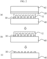
- FIG. 2 is a cross-sectional view schematically showing a process of transferring the nanowire array in the method for manufacturing the surface-enhanced Raman spectroscopy substrate according to one embodiment of the present disclosure.
- FIG. 3 is a plan view showing a single layer of a nanolattice in the method for manufacturing the surface-enhanced Raman spectroscopy substrate according to one embodiment of the present disclosure.
- a master mold 10 having a surface on which a pattern is formed may be coated with a polymer to form a duplication mold 12.
- a concavo-convex surface (the surface on which the pattern is formed) of the master mold 10 may be coated with a polymer composition including the polymer and a solvent by using spin coating, deep coating, or spray coating, and the solvent may be removed (dried), so that the duplication mold 12 may be formed.
- the concavo-convex surface of the master mold 10 may have a shape in which protrusions and recesses are repeatedly formed in a horizontal direction.
- a horizontal length of the protrusion and a horizontal length of the recess may be equal to or different from each other, and may be variously adjusted according to a shape and a pitch of the pattern to be transferred.
- the duplication mold 12 may include, but is not limited to, polymethyl methacrylate (PMMA), polystyrene, poly-4-viyl pyridine, or a combination thereof, and may be formed of various polymer materials.
- the duplication mold 12 may have a single-layer structure or a multilayer structure including mutually different materials.
- SAM self-assembled monolayer
- a PDMS brush polymer having low surface energy or a hydrophobic material such as hexamethylene disilazane (HMDS) may be performed on the surface of the master mold 10, on which the pattern is formed, in advance, so that the duplication mold 12 may be easily separated from the master mold 10 in the following step.
- HMDS hexamethylene disilazane
- the duplication mold 12 may be separated from the master mold 10.
- an adhesive film 20 may be attached to a top surface of the duplication mold 12 (a surface that is opposite to a surface of the duplication mold on which a pattern is transferred), and an external force may be applied, so that the duplication mold 12 and the master mold 10 may be physically separated from each other.
- An adhesive surface of the adhesive film 20 may be coated with an adhesive.
- the duplication mold 12 may have a concavo-convex pattern corresponding to an inverse shape of the pattern of the surface of the master mold 10.
- a functional material may be deposited on a partial region of the duplication mold 12 to form a nanowire array 30.
- the duplication mold is tilted such that the surface of the duplication mold 12 on which the deposition is performed and a deposition direction may have a predetermined angle
- the functional material may be deposited only on the partial region including and surrounding a protruding portion (edge) of the pattern of the surface of the duplication mold 12. Accordingly, a pattern of the functional material may be obtained without a photolithography process.
- the nanowire array 30 may be formed through the inclined deposition.
- the functional material may include a metal such as Au, Ag, Cu, Ni, Pt, Cr, Co, or Pd, but embodiments of the present disclosure are not limited thereto, and various materials may be used as the functional material as necessary.
- the nanowire array 30 may be transferred to a transfer substrate.
- the nanowire array 30 may be brought into contact with a surface of the transfer substrate 40, and the adhesive film 20 may be pressed and heated by using a pressing member 42. Accordingly, bonding strength between the adhesive film 20 and the duplication mold 12 may be weakened by the heat, so that the adhesive film 20 may be easily removed from the duplication mold 12.
- a heating temperature may be greater than or equal to 100 °C, for example, 100 °C to 300 °C, but the embodiments of the present disclosure are not limited thereto.
- the duplication mold 12 remaining on the nanowire array 30 may be removed by using a solvent.
- a solvent such as toluene, acetone, or isopropyl alcohol may be provided to the duplication mold 12 to remove the duplication mold 12.
- the nanowire array 30 may be transferred onto the transfer substrate 40.
- a line width of the nanowire array 30 may be 10 nm to 100 nm
- a pitch of the nanowire array 30 may be 20 nm to 500 nm, but the line width and the pitch are not limited thereto.
- the above process may be repeatedly performed to form a nanolattice.
- a first nanowire array 32 including a plurality of nanowires extending in a first direction D1 may be formed on the transfer substrate.
- the process shown in FIG. 1 may be repeatedly performed to form the nanowire array on the duplication mold, heat-assisted transfer may be performed in a method shown in FIG. 2 on the transfer substrate 40 onto which the first nanowire array 32 is transferred such that the first nanowire array 32 and an additional nanowire array may intersect each other, so that a nanolattice including a second nanowire array 34 may be formed.
- the second nanowire array 34 may include a plurality of nanowires extending in a second direction D2 perpendicular to the first direction D1.
- An opening of the nanolattice may be defined between adjacent nanowires of the first nanowire array 32 and between adjacent nanowires of the second nanowire array 34.
- a contact region JT intersection region of the first nanowire array 32 and the second nanowire array 34 may be welded. Accordingly, stability of the nanolattice may be improved, and the nanolattice may be prevented from being deformed or damaged in subsequent processes.
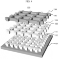
- FIG. 4 is an exploded perspective view showing a surface-enhanced Raman spectroscopy substrate according to one embodiment of the present disclosure.
- FIG. 5 is a schematic view showing immobilizing of an antibody on the surface-enhanced Raman spectroscopy substrate according to one embodiment of the present disclosure.
- a surface-enhanced Raman spectroscopy substrate 100 may include a multi-stage nanolattice structure.
- the multi-stage nanolattice structure may include a first nanolattice 110, a second nanolattice 120 disposed on the first nanolattice 110, and a third nanolattice 130 disposed on the second nanolattice 120.
- the multi-stage nanolattice structure may be disposed on a base substrate 101.
- the base substrate 101 may be conductive, or may include an electrode (conductive terminal) electrically connected to the multi-stage nanolattice structure.
- the nanolattices of the multi-stage nanolattice structure may include mutually different materials.
- the first nanolattice 110 may include Ag
- the second nanolattice 120 may include Au
- the third nanolattice 130 may include Pt.
- the third nanolattice 130 including Pt may be heated.
- the heated Pt may have increased crystallinity, which may improve a surface enhancement effect.
- the surface enhancement effect of Pt which is lower than a surface enhancement effect of each of Ag and Au, may be improved so as to be used as a material for the surface-enhanced Raman spectroscopy substrate.
- a heating temperature for Pt may be 500 °C to 850 °C, and preferably 650 °C to 800 °C.
- the heating temperature is excessively high, the crystallinity may be reduced by melting so that the surface enhancement effect may not be increased.
- the nanolattices may have mutually different pitches.
- the first nanolattice 110 may have a first pitch (hereinafter, the pitch may refer to a pitch between adjacent nanowires)
- the second nanolattice 120 may have a second pitch that is greater than the first pitch
- the third nanolattice 130 may have a third pitch that is greater than the second pitch.
- a size (an area when viewed in plan view) of an opening (a unit opening) of the second nanolattice 120 may be greater than a size of an opening of the first nanolattice 110
- a size of an opening of the third nanolattice 130 may be greater than the size of the opening of the second nanolattice 120.
- the nanowire of the second nanolattice 120 and the nanowire of the first nanolattice 110 may be exposed through the opening of the third nanolattice 130.
- the opening of the third nanolattice 130 may overlap the nanowire of the second nanolattice 120 and the nanowire of the first nanolattice 110.
- the lower nanolattice since the size of the opening the upper nanolattice is greater than the size of the opening of the lower nanolattice in the multi-stage nanolattice structure, the lower nanolattice may be easily exposed to a target material coming from a top of the multi-stage nanolattice structure. In addition, a deviation between areas of the nanolattices exposed to the sample may be reduced to improve reliability of detection.
- a nanolattice formed of a material having a relatively large surface enhancement effect may be disposed in a lower portion (a region in which the surface enhancement effect is reduced by an upper layer), and a nanolattice formed of a material having a relatively small surface enhancement effect may be disposed in an upper portion, so that a decrease in the reliability of the detection caused by the difference between the surface enhancement effects may be prevented.
- Each of the nanolattices of the multi-stage nanolattice structure may be formed through the method described with reference to FIGS. 1 to 3 .
- the transfer substrate of the nanolattice is removed through an etchant or the like, and the nanolattice is brought into contact with another nanolattice, the nanolattices may be bound to each other by a van der Waals' force or the like without a separate adhesive, so that the multi-stage nanolattice structure may be formed.
- the surface-enhanced Raman spectroscopy substrate may be used to detect a biomarker, and more particularly, the surface-enhanced Raman spectroscopy substrate may be effectively used for multiple detection of biomarkers.
- the nanolattices may be designed to be selectively bound to mutually different biomarkers, respectively.
- the first nanolattice 110 may include a first antibody 114
- the second nanolattice 120 may include a second antibody 124
- the third nanolattice 130 may include a third antibody 134.
- the antibodies may be bound to mutually different target materials (biomarkers) through antigen-antibody binding, respectively.
- the target materials may be bound to aptamers connected to mutually different Raman labels according to types of the target materials, respectively.
- a linker such as dithiobis-N-succinimidyl propionate (DTSP) may be used.
- DTSP dithiobis-N-succinimidyl propionate
- the DTSP may be provided to the nanolattice 110 to form a linker 112 on a surface of the nanolattice, and the antibody 114 may be bound to the linker.
- Immobilizing of an antibody on each of the nanolattices may be performed after each of the nanolattices is formed, and subsequently, the nanolattices may be bound to each other to form the multi-stage nanolattice structure.
- the heating of the Pt nanolattice may be performed after the nanolattice including Pt is formed, and subsequently, the antibody may be immobilized on the Pt nanolattice.
- the nanolattices are formed of mutually different materials according to the embodiments of the present disclosure
- reduction voltage peaks having mutually different values may be observed by the nanolattices.
- Characteristics (a current value, an area, etc.) of the reduction voltage peak may vary according to an amount of target materials bound to each of the nanolattices. Accordingly, after the substrate reacts with the sample, each of the bound target materials or the target materials included in the sample may be quantified based on a variation in a reduction voltage peak (before/after the reaction) obtained through the cyclic voltammetry measurement.
- a method for detecting a biomarker may include: allowing a sample including a biomarker to make contact with a surface-enhanced Raman spectroscopy substrate including a multi-stage nanolattice structure; identifying a biomarker bound to the surface-enhanced Raman spectroscopy substrate through Raman spectroscopy analysis; and quantifying the biomarker through cyclic voltammetry measurement of the multi-stage nanolattice structure.
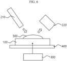
- FIG. 6 is a schematic view schematically showing a system for detecting a biomarker according to one embodiment of the present disclosure.
- a system for detecting a biomarker may include: a surface-enhanced Raman spectroscopy substrate 100 bindable with a biomarker in a sample 500; a light source 210 configured to emit a light to the surface-enhanced Raman spectroscopy substrate bound to the biomarker; an identifying part 220 configured to identify the biomarker by analyzing Raman spectroscopy of the light reflected from the surface-enhanced Raman spectroscopy substrate; and a quantifying part 300 configured to quantify the biomarker through cyclic voltammetry measurement of the surface-enhanced Raman spectroscopy substrate on which the biomarker is collected.
- the system may further include a stage 400 configured to support the surface-enhanced Raman spectroscopy substrate 100.
- the surface-enhanced Raman spectroscopy substrate may be identical to the surface-enhanced Raman spectroscopy substrate described above.
- FIG. 7 is a schematic view for describing a method for detecting a biomarker according to one embodiment of the present disclosure.
- a sample may be brought into contact with a nanolattice 110 of a multi-stage nanolattice structure having an antibody bound to a surface of the multi-stage nanolattice structure, so that a biomarker Target in the sample may be bound to the antibody.
- an appropriate amount of sample may be dropped onto the surface-enhanced Raman spectroscopy substrate, and contact may be maintained for a sufficient time for the biomarker in the sample to be bound to the antibody.
- the substrate may be moved or rotated so that the antibody and the biomarker may be easily bound to each other.
- the biomarker may be derived from a biological organism.
- the sample may include a biological fluid.
- the biological fluid may include urine, blood, plasma, serum, saliva, semen, excrement, sputum, a cerebrospinal fluid, a tear, mucus, an amniotic fluid, and the like.
- the sample may include a biological tissue of a humans, an animal, a plant, a bacterium, a mycete, and a virus, a cell thereof, or an intracellular material thereof.
- the sample may include an environmental sample such as drinking water or food.
- an aptamer bound to a Raman label may be bound to the biomarker.
- the biomarker is a protein, detection of a peak distinguished through Raman spectroscopy analysis may not be easily performed.
- mutually different Raman labels may be bound according to a type of the biomarker, and a peak corresponding to the Raman label may be determined, so that reliability of multiple detection may be improved.
- aptamers When a plurality of biomarkers are to be detected, mutually different aptamers that may be selectively bound to the biomarkers, respectively, may be used, and the aptamers may be bound to mutually different Raman labels, respectively.
- the following Table 1 shows biomarkers used in diagnosis of lung cancer.
- diagnosis accuracy is high (with a sensitivity of 75% and a specificity of 82%) when the diagnosis is performed through a combination of carcinoembryonic antigen (CEA), CYFRA 21-1, and neuron-specific enolase (NSE).
- CEA carcinoembryonic antigen
- CYFRA 21-1 CYFRA 21-1
- NSE neuron-specific enolase
- CEA Carcinoembryonic Antigen
- RBP Retinol-binding protein
- A1AT squamous cell carcinoma antigen CA-125 ⁇ -Fetoprotein (AFP)
- AFP ⁇ CYFRA 21-1 chromogranin A
- NSE neuron-specific enolase
- a structure of an aptamer corresponding to (bindable to) the biomarker has been known as follows.
- CEA aptamer DNA aptamer 5'-ATACCAGCTTATTCAATT-3' Ref: J. Mater. Chem. B, 2017, 5, 1594-1600
- CYFRA 21-1 aptamer DNA aptamer : 5'-CGCCCCTGACACCATTCCTCCCTTC-3' Ref: https://doi.org/10.1016/j.chemosphere.2022.134636
- NSE Neuron-specific enolase
- DNA aptamer 5'-TCACACACGGACCTCTCCTACATTAATTGCGCATTTCGTT-3' Ref: https://pubs.rsc.org/en/content/articlepdf/2079/re/c9ra00785g : RSC Adv., 2019, 9, 15513
- a first aptamer that may be selectively bound to the CEA, a second aptamer that may be selectively bound to the CYFRA 21-1, and a third aptamer that may be selectively bound to the NSE may be provided to the substrate so as to be bound to the corresponding biomarkers.
- the first to third aptamers may be bound to mutually different labels.
- the labels may be bound to a head and/or a tail of the aptamers.
- the labels are for distinguishing the biomarkers from each other, it may be preferable that Raman peaks by the labels are easily distinguished from each other, and it may be preferable that Raman cross-sections are similar to each other in order to identify each of the Raman peaks.
- a combination of a plurality of labels (dyes) to be bound to the first to third aptamers may include rhodamine 6G (R6G), methylene blue (MB), and malachite green (MG).
- R6G rhodamine 6G
- MB methylene blue
- MG malachite green
- the label-aptamer combination does not have to be specified, while the same label has to be bound to the same aptamers.
- the first aptamer may be bound to the R6G
- the second aptamer may be bound to the MB
- the third aptamer may be bound to the MG.
- a first nanolattice including Ag may be bound to a CYFRA 21-1-specific antibody, in which the aptamer bound to the MB may be used to label the CYFRA 21-1, a second nanolattice including Au may be bound to an NSE-specific antibody, in which the aptamer bound to the R6G may be used to label the NSE, and a third nanolattice including Pt may be bound to a CEA-specific antibody, in which the aptamer bound to the MG may be used to label the CEA.
- the following method may be considered so that the intensity of the Raman peak of each of the labels is located within a predetermined range.
- concentrations of the aptamers may be different from each other.
- concentrations of the aptamers may be greater than a concentration of each of the first aptamer and the second aptamer.
- the numbers of the labels bound to the aptamers may be different from each other.
- the Raman peak of the MG is weak
- the MG may be bound to both the head and the tail of the third aptamer
- the label may be bound to one of the head or the tail of the first aptamer and the second aptamer.
- the quantifying part 300 may perform the cyclic voltammetry measurement of the surface-enhanced Raman spectroscopy substrate bound to the biomarker to quantify the biomarker based on the cyclic voltammetry measurement.
- the surface-enhanced Raman spectroscopy substrate may include a plurality of nanolattices including mutually different materials. Therefore, when the cyclic voltammetry measurement of the surface-enhanced Raman spectroscopy substrate is performed, reduction voltage peaks having mutually different values may be observed by the nanolattices. Characteristics (a current value, an area, etc.) of the reduction voltage peak may vary according to an amount of biomarkers bound to each of the nanolattices. Accordingly, after the substrate reacts with the sample to bind the substrate to the biomarker, the amount of the biomarkers may be calculated based on a variation in a reduction voltage peak (before/after the reaction) obtained through the cyclic voltammetry measurement. Accordingly, the biomarkers bound to the substrate or the biomarkers included in the sample may be distinguished and quantified. In addition, various known calibrations may be used for the quantification based on the cyclic voltammetry measurement.
- a target material may be rapidly detected by using surface-enhanced Raman spectroscopy.
- a plurality of target materials may be simultaneously detected by using a multi-stage nanolattice structure that may be selectively bound to mutually different materials.
- nanolattices may have mutually different pitches within a multi-stage nanolattice structure, so that a surface enhancement effect of a lower nanolattice may be prevented from deteriorating.
- a surface enhancement effect may be increased through heating of Pt, which is known to have a low surface enhancement effect.
- identification and quantification of a target material may be performed through a combination of surface-enhanced Raman spectroscopy and cyclic voltammetry.
- multiple detection of biomarkers that are difficult to be identified and distinguished, such as proteins, may be performed by using an aptamer bound to a label.
- accuracy of multiple detection may be improved through a combination of labels suitable for the multiple detection, and the accuracy of the multiple detection may be improved by varying the number of labels bound to the aptamer.
- the duplication mold While the duplication mold is tilted, deposition was performed to form a first Ag nanowire array.
- the first Ag nanowire array was placed on a SiO 2 wafer substrate, heated (150 °C), and pressed, and the adhesive film was removed. After the adhesive film is removed, isopropyl alcohol was applied to remove the duplication mold, and the first Ag nanowire array was transferred to the SiO 2 wafer substrate.
- a second Ag nanowire array was formed in the same way as the first Ag nanowire array, and brought into contact with the first Ag nanowire array to intersect the first Ag nanowire array when viewed in a plan view.
- heating-pressing was performed, an adhesive film was removed, and a duplication mold was removed, so that a first nanolattice including the first Ag nanowire array and the second Ag nanowire array, which are welded to each other in a contact region, was prepared.
- DMSO dimethyl sulfoxide
- the first nanolattice was immersed in a PBS solution (1 to 2 g/ml) including a CYFRA21-1-specific antibody (monoclonal antibody) for 4 hours, immersed in a PBS solution including 10% ethanolamine for 4 hours, and washed with 0.1M Tris-HCl (pH 8.0).
- the duplication mold While the duplication mold is tilted, deposition was performed to form a first Au nanowire array.
- the first Au nanowire array was placed on a SiO 2 wafer substrate, heated (150 °C), and pressed, and the adhesive film was removed. After the adhesive film is removed, isopropyl alcohol was applied to remove the duplication mold, and the first Au nanowire array was transferred to the SiO 2 wafer substrate.
- a second Au nanowire array was formed in the same way as the first Au nanowire array, and brought into contact with the first Au nanowire array to intersect the first Au nanowire array when viewed in a plan view.
- heating-pressing was performed, an adhesive film was removed, and a duplication mold was removed, so that a second nanolattice including the first Au nanowire array and the second Au nanowire array, which are welded to each other in a contact region, was prepared.
- a DMSO solution NaBH 4 75 mM in which DTSP (3 mg/mL) is dissolved was incubated for 30 minutes, the second nanolattice was immersed in the solution for 30 minutes, and the second nanolattice was washed with DMSO and deionized water.
- the second nanolattice was immersed in a PBS solution (1 to 2 g/ml) including an NSE-specific antibody for 4 hours, immersed in a PBS solution including 10% ethanolamine for 4 hours, and washed with 0.1M Tris-HCl (pH 8.0).
- a concavo-convex surface of a master mold having a pitch of 200 nm (where a protrusion width is 50 nm, and a recess width is 150 nm) was coated with PMMA, and dried to form a duplication mold. After an adhesive film is attached to a top surface of the duplication mold, the duplication mold was separated from the master mold.
- the duplication mold While the duplication mold is tilted, deposition was performed to form a first Pt nanowire array.
- the first Pt nanowire array was placed on a SiO 2 wafer substrate, heated (150 °C), and pressed, and the adhesive film was removed. After the adhesive film is removed, isopropyl alcohol was applied to remove the duplication mold, and the first Pt nanowire array was transferred to the SiO 2 wafer substrate.
- a second Pt nanowire array was formed in the same way as the first Pt nanowire array, and brought into contact with the first Pt nanowire array to intersect the first Pt nanowire array when viewed in a plan view.
- heating-pressing was performed, an adhesive film was removed, and a duplication mold was removed, so that a third nanolattice including the first Pt nanowire array and the second Pt nanowire array, which are welded to each other in a contact region, was prepared.
- the third nanolattice was heated by performing heating in an Ar atmosphere for 1 minute or more.
- a DMSO solution NaBH 4 75 mM in which DTSP (3 mg/mL) is dissolved was incubated for 30 minutes, the third nanolattice was immersed in the solution for 30 minutes, and the third nanolattice was washed with DMSO and deionized water.
- the third nanolattice was immersed in a PBS solution (1 to 2 g/ml) including a CEA-specific antibody for 4 hours, immersed in a PBS solution including 10% ethanolamine for 4 hours, and washed with 0.1M Tris-HCl (pH 8.0).
- the separated second nanolattice was floated on purified water, and water transfer was performed on the first nanolattice.
- the separated third nanolattice was floated on purified water, and water transfer was performed on the second nanolattice disposed on the first nanolattice.
- FIG. 8 is a graph showing Raman spectroscopy obtained after dropping R6G (10 -6 M) on a third nanolattice according to Example 1.
- a surface enhancement effect is increased at a heating temperature of 500 °C or more, and it was found that the surface enhancement effect is increased most significantly at 700 °C, while the surface enhancement effect is decreased at 900 °C.
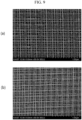
- FIG. 9 shows a scanning electron microscope (SEM) photograph (a) after a second nanolattice is transferred onto a first nanolattice, and an SEM photograph (b) after the third nanolattice is transferred onto the second nanolattice according to Example 1.
- SEM scanning electron microscope
- a lower nanolattice may be exposed by varying the pitch of each of the nanolattices.
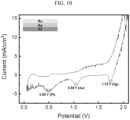
- FIG. 10 is a graph showing a result of cyclic voltammetry measurement of a multi-stage nanolattice structure according to Example 1.
- Embodiments of the present disclosure may be used for detecting various materials, which can be detecded through surface-enhanced Raman spectroscopy analysis, including a biomarker.
Landscapes
- Health & Medical Sciences (AREA)
- Life Sciences & Earth Sciences (AREA)
- Chemical & Material Sciences (AREA)
- Physics & Mathematics (AREA)
- Immunology (AREA)
- Molecular Biology (AREA)
- General Physics & Mathematics (AREA)
- Biochemistry (AREA)
- Analytical Chemistry (AREA)
- General Health & Medical Sciences (AREA)
- Pathology (AREA)
- Spectroscopy & Molecular Physics (AREA)
- Engineering & Computer Science (AREA)
- Chemical Kinetics & Catalysis (AREA)
- Electrochemistry (AREA)
- Biomedical Technology (AREA)
- Urology & Nephrology (AREA)
- Hematology (AREA)
- Nuclear Medicine, Radiotherapy & Molecular Imaging (AREA)
- Nanotechnology (AREA)
- Biotechnology (AREA)
- Cell Biology (AREA)
- Microbiology (AREA)
- Food Science & Technology (AREA)
- Medicinal Chemistry (AREA)
- Inorganic Chemistry (AREA)
- Investigating, Analyzing Materials By Fluorescence Or Luminescence (AREA)
Abstract
A surface-enhanced Raman spectroscopy substrate includes a multi-stage nanolattice structure including a first nanolattice including silver (Ag), a second nanolattice including gold (Au), and a third nanolattice including platinum (Pt). The surface-enhanced Raman spectroscopy substrate may be used for detecting different target materials.
Description
- This application claims priority under 35 USC § 119 to
Korean Patent Application No. 10-2023-0098228 filed on July 27, 2023 - Embodiments of the present disclosure relate to a detection system using surface-enhanced Raman spectroscopy. More particularly, embodiments of the present disclosure relate to a surface-enhanced Raman spectroscopy substrate, and a method and a system for detecting a biomarker by using surface-enhanced Raman spectroscopy and cyclic voltammetry.
- Biomarkers are biological indicators capable of detecting a variation in a body caused by occurrence of a disease or the like with molecular information including DNA, RNA, metabolites, proteins, and the like. The biomarkers may be used for diagnosis and prognosis observation of a disease, a customized medical technology, and development of an intelligent healthcare system for establishing a patient-friendly treatment environment. For example, biomarkers that are being clinically used for cancer diagnosis include prostate-specific antigen (PSA), carcinoembryonic antigen (CEA), and alpha-fetoprotein (AFP).
- However, diagnosis using a single biomarker may have low accuracy. For example, according to meta-analysis, in a case of the PSA, a sensitivity for prostate cancer remains at about 70%, and a specificity for prostate cancer remains at 58%. In addition, one biomarker is frequently involved in a plurality of cancer types. Therefore, recently, a multi-biomarker panel-based diagnosis that simultaneously uses a plurality of biomarkers has been studied.
- Multiplexing biosensors currently under development have a horizontal array-type sensor structure, and measure and quantify a plurality of biomarkers, respectively, which increases required clinical samples, measurement time, and cost. It is difficult to accurately quantify each of components due to false positive problems and mutual interference effects caused by non-specific binding of antibodies, aptamers, and the like used in a selective binding process of biomarkers.
-
- 1)
Korean Unexamined Patent Publication No. 2021-0137215 - 2)
Korean Unexamined Patent Publication No. 2014-0140179 - 3)
Korean Patent Registration No. 1589039 - One object of the present disclosure is to provide a surface-enhanced Raman spectroscopy substrate that is usable for multiple detection.
- Another object of the present disclosure is to provide a detection method capable of improving accuracy of detection and quantification of a plurality of target materials.
- Still another object of the present disclosure is to provide a detection system capable of improving accuracy of detection and quantification of a plurality of target materials.
- According to an embodiment of the present disclosure, a surface-enhanced Raman spectroscopy substrate includes a multi-stage nanolattice structure including a first nanolattice including silver (Ag), a second nanolattice including gold (Au), and a third nanolattice including platinum (Pt).
- In an embodiment, at least one of the first nanolattice, the second nanolattice, and the third nanolattice includes a first nanowire array including a plurality of nanowires extending in a first direction and a second nanowire array including a plurality of nanowires extending in a second direction intersecting the first direction. The the first nanowire array and the second nanowire array are welded in a contact region.
- In an embodiment, the second nanolattice is disposed on the first nanolattice, and the third nanolattice is disposed on the second nanolattice.
- In an embodiment, the second nanolattice has a pitch greater than a pitch of the first nanolattice, and the third nanolattice has a pitch greater than the pitch of the second nanolattice.
- In an embodiment, each of the first to third nanolattices includes a plurality of nanowires. The nanowire of the first nanolattice and the nanowire of the second nanolattice are exposed through an opening of the third nanolattice.
- In an embodiment, the first to third nanolattices have mutually different pitches.
- In an embodiment, the first to third nanolattices have antibodies immobilized on surfaces of the first to third nanolattices, respectively.
- In an embodiment, the antibodies immobilized on the first to third nanolattices are different from each other.
- In an embodiment, the third nanolattice is heated at 500 °C to 850 °C.
- According to an embodiment of the present disclosure, a method for detecting a biomarker includes allowing a sample including a biomarker to make contact with a surface-enhanced Raman spectroscopy substrate including a multi-stage nanolattice structure, identifying a biomarker bound to the surface-enhanced Raman spectroscopy substrate through Raman spectroscopy analysis, and quantifying the biomarker through cyclic voltammetry measurement of the multi-stage nanolattice structure.
- In an embodiment, the method further includes binding an aptamer, which is bound to a Raman label, to the biomarker bound to the surface-enhanced Raman spectroscopy substrate before performing the Raman spectroscopy analysis.
- In an embodiment, the multi-stage nanolattice structure includes at least three nanolattices including mutually different materials. The aptamer includes a first aptamer bound to rhodamine 6G (R6G), a second aptamer bound to methylene blue (MB), and a third aptamer bound to malachite green (MG).
- In an embodiment, a concentration of the third aptamer is greater than each of a concentration of the first aptamer and a concentration of the second aptamer.
- In an embodiment, the malachite green is bound to both a head and a tail of the third aptamer. The rhodamine 6G and the methylene blue are bound to one of a head or a tail of the first aptamer and the second aptamer.
- In an embodiment, the multi-stage nanolattice structure includes a plurality of nanolattices including mutually different materials. The quantifying of the biomarker includes performing the cyclic voltammetry measurement of the multi-stage nanolattice structure, and calculating an amount of the biomarker based on a variation of a reduction voltage peak corresponding to the material of each of the nanolattices from a result obtained through the cyclic voltammetry measurement.
- According to an embodiment of the present disclosure, a system for detecting a biomarker includes a surface-enhanced Raman spectroscopy substrate including a multi-stage nanolattice structure bindable with a plurality of biomarkers in a sample; a light source configured to emit a light to the surface-enhanced Raman spectroscopy substrate bound to the biomarker; an identifying part configured to identify the biomarker by analyzing Raman spectroscopy of the light reflected from the surface-enhanced Raman spectroscopy substrate; and a quantifying part configured to quantify the biomarker through cyclic voltammetry measurement of the surface-enhanced Raman spectroscopy substrate on which the biomarker is collected.
- According to the embodiments, a target material may be rapidly detected by using surface-enhanced Raman spectroscopy.
- In addition, a plurality of target materials may be simultaneously detected by using a multi-stage nanolattice structure that may be selectively bound to mutually different materials.
- In addition, nanolattices may have mutually different pitches within a multi-stage nanolattice structure, so that a surface enhancement effect of a lower nanolattice may be prevented from deteriorating.
- In addition, a surface enhancement effect may be increased through heating of Pt, which is known to have a low surface enhancement effect.
- In addition, identification and quantification of a target material may be performed through a combination of surface-enhanced Raman spectroscopy and cyclic voltammetry.
- In addition, multiple detection of biomarkers that are difficult to be identified and distinguished, such as proteins, may be performed by using an aptamer bound to a label.
- In addition, accuracy of multiple detection may be improved through a combination of labels suitable for the multiple detection, and the accuracy of the multiple detection may be improved by varying the number of labels bound to the aptamer.
-
-
FIG. 1 is a cross-sectional view schematically showing a process of forming a nanowire array in a method for manufacturing a surface-enhanced Raman spectroscopy substrate according to one embodiment of the present disclosure. -
FIG. 2 is a cross-sectional view schematically showing a process of transferring the nanowire array in the method for manufacturing the surface-enhanced Raman spectroscopy substrate according to one embodiment of the present disclosure. -
FIG. 3 is a plan view showing a single layer of a nanolattice in the method for manufacturing the surface-enhanced Raman spectroscopy substrate according to one embodiment of the present disclosure. -
FIG. 4 is an exploded perspective view showing a surface-enhanced Raman spectroscopy substrate according to one embodiment of the present disclosure. -
FIG. 5 is a schematic view showing immobilizing of an antibody on the surface-enhanced Raman spectroscopy substrate according to one embodiment of the present disclosure. -
FIG. 6 is a schematic view schematically showing a system for detecting a biomarker according to one embodiment of the present disclosure. -
FIG. 7 is a schematic view for describing a method for detecting a biomarker according to one embodiment of the present disclosure. -
FIG. 8 is a graph showing Raman spectroscopy obtained after dropping R6G (10-6 M) on a third nanolattice according to Example 1. -
FIG. 9 shows a scanning electron microscope (SEM) photograph (a) after a second nanolattice is transferred onto a first nanolattice, and an SEM photograph (b) after the third nanolattice is transferred onto the second nanolattice according to Example 1. -
FIG. 10 is a graph showing a result of cyclic voltammetry measurement of a multi-stage nanolattice structure according to Example 1. - Various embodiments will be described more fully hereinafter with reference to the accompanying drawings, in which some embodiments are shown. The invention may, however, be embodied in many different forms and should not be construed as limited to the embodiments set forth herein. Rather, these embodiments are provided so that this description will be thorough and complete, and will fully convey the scope of the invention to those skilled in the art. In the drawings, the sizes and relative sizes of layers and regions may be exaggerated for clarity.
- It will be understood that when an element or layer is referred to as being "on," "connected to" or "coupled to" another element or layer, it can be directly on, connected or coupled to the other element or layer or intervening elements or layers may be present. In contrast, when an element is referred to as being "directly on," "directly connected to" or "directly coupled to" another element or layer, there are no intervening elements or layers present. Like numerals refer to like elements throughout. As used herein, the term "and/or" includes any and all combinations of one or more of the associated listed items.
- It will be understood that, although the terms first, second, third etc. may be used herein to describe various elements, components, regions, layers and/or sections, these elements, components, regions, layers and/or sections should not be limited by these terms. These terms are only used to distinguish one element, component, region, layer or section from another region, layer or section. Thus, a first element, component, region, layer or section discussed below could be termed a second element, component, region, layer or section without departing from the teachings of the invention.
- The terminology used herein is for the purpose of describing particular embodiments only and is not intended to be limiting of the invention. As used herein, the singular forms "a," "an" and "the" are intended to include a plurality of forms as well, unless the context clearly indicates otherwise. It will be further understood that the terms "comprises" and/or "comprising," when used in this specification, specify the presence of stated features, integers, steps, operations, elements, and/or components, but do not preclude the presence or addition of one or more other features, integers, steps, operations, elements, components, and/or groups thereof.
- Unless otherwise defined, all terms (including technical and scientific terms) used herein have the same meaning as commonly understood by one of ordinary skill in the art to which this invention belongs. It will be further understood that terms, such as those defined in commonly used dictionaries, should be interpreted as having a meaning that is consistent with their meaning in the context of the relevant art and will not be interpreted in an idealized or overly formal sense unless expressly so defined herein.
- According to one embodiment of the present disclosure, a surface-enhanced Raman spectroscopy substrate may be manufactured by using thermally assisted nanotransfer printing (T-nTP).
-
FIG. 1 is a cross-sectional view schematically showing a process of forming a nanowire array in a method for manufacturing a surface-enhanced Raman spectroscopy substrate according to one embodiment of the present disclosure.FIG. 2 is a cross-sectional view schematically showing a process of transferring the nanowire array in the method for manufacturing the surface-enhanced Raman spectroscopy substrate according to one embodiment of the present disclosure.FIG. 3 is a plan view showing a single layer of a nanolattice in the method for manufacturing the surface-enhanced Raman spectroscopy substrate according to one embodiment of the present disclosure. - Referring to (a) of
FIG. 1 , amaster mold 10 having a surface on which a pattern is formed may be coated with a polymer to form aduplication mold 12. For example, a concavo-convex surface (the surface on which the pattern is formed) of themaster mold 10 may be coated with a polymer composition including the polymer and a solvent by using spin coating, deep coating, or spray coating, and the solvent may be removed (dried), so that theduplication mold 12 may be formed. When viewed in a cross-sectional view, the concavo-convex surface of themaster mold 10 may have a shape in which protrusions and recesses are repeatedly formed in a horizontal direction. In addition, a horizontal length of the protrusion and a horizontal length of the recess may be equal to or different from each other, and may be variously adjusted according to a shape and a pitch of the pattern to be transferred. - For example, the
duplication mold 12 may include, but is not limited to, polymethyl methacrylate (PMMA), polystyrene, poly-4-viyl pyridine, or a combination thereof, and may be formed of various polymer materials. In addition, theduplication mold 12 may have a single-layer structure or a multilayer structure including mutually different materials. - In addition, self-assembled monolayer (SAM) coating using a PDMS brush polymer having low surface energy or a hydrophobic material such as hexamethylene disilazane (HMDS) may be performed on the surface of the
master mold 10, on which the pattern is formed, in advance, so that theduplication mold 12 may be easily separated from themaster mold 10 in the following step. - Referring to (b) of
FIG. 1 , theduplication mold 12 may be separated from themaster mold 10. According to one embodiment, anadhesive film 20 may be attached to a top surface of the duplication mold 12 (a surface that is opposite to a surface of the duplication mold on which a pattern is transferred), and an external force may be applied, so that theduplication mold 12 and themaster mold 10 may be physically separated from each other. An adhesive surface of theadhesive film 20 may be coated with an adhesive. - Since the
duplication mold 12 is formed to fill a concavo-convex portion of the pattern of the surface of themaster mold 10, theduplication mold 12 may have a concavo-convex pattern corresponding to an inverse shape of the pattern of the surface of themaster mold 10. - Referring to (c) and (d) of
FIG. 1 , a functional material may be deposited on a partial region of theduplication mold 12 to form ananowire array 30. According to one embodiment, while the duplication mold is tilted such that the surface of theduplication mold 12 on which the deposition is performed and a deposition direction may have a predetermined angle, when E-beam lithography, thermal evaporation, sputtering, or the like is performed, the functional material may be deposited only on the partial region including and surrounding a protruding portion (edge) of the pattern of the surface of theduplication mold 12. Accordingly, a pattern of the functional material may be obtained without a photolithography process. For example, when the pattern of the surface of theduplication mold 12 has a wire array shape (when the protrusion or the recess has a shape extending in one direction), thenanowire array 30 may be formed through the inclined deposition. - The functional material may include a metal such as Au, Ag, Cu, Ni, Pt, Cr, Co, or Pd, but embodiments of the present disclosure are not limited thereto, and various materials may be used as the functional material as necessary.
- Next, the
nanowire array 30 may be transferred to a transfer substrate. - Referring to (a) and (b) of
FIG. 2 , thenanowire array 30 may be brought into contact with a surface of thetransfer substrate 40, and theadhesive film 20 may be pressed and heated by using a pressingmember 42. Accordingly, bonding strength between theadhesive film 20 and theduplication mold 12 may be weakened by the heat, so that theadhesive film 20 may be easily removed from theduplication mold 12. A heating temperature may be greater than or equal to 100 °C, for example, 100 °C to 300 °C, but the embodiments of the present disclosure are not limited thereto. - The
duplication mold 12 remaining on thenanowire array 30 may be removed by using a solvent. For example, in order to remove theduplication mold 12, an organic solvent such as toluene, acetone, or isopropyl alcohol may be provided to theduplication mold 12 to remove theduplication mold 12. - As a result, as shown in (c) of
FIG. 2 , thenanowire array 30 may be transferred onto thetransfer substrate 40. For example, a line width of thenanowire array 30 may be 10 nm to 100 nm, and a pitch of thenanowire array 30 may be 20 nm to 500 nm, but the line width and the pitch are not limited thereto. - According to one embodiment, the above process may be repeatedly performed to form a nanolattice. For example, referring to
FIG. 3 , afirst nanowire array 32 including a plurality of nanowires extending in a first direction D1 may be formed on the transfer substrate. The process shown inFIG. 1 may be repeatedly performed to form the nanowire array on the duplication mold, heat-assisted transfer may be performed in a method shown inFIG. 2 on thetransfer substrate 40 onto which thefirst nanowire array 32 is transferred such that thefirst nanowire array 32 and an additional nanowire array may intersect each other, so that a nanolattice including asecond nanowire array 34 may be formed. For example, thesecond nanowire array 34 may include a plurality of nanowires extending in a second direction D2 perpendicular to the first direction D1. - An opening of the nanolattice may be defined between adjacent nanowires of the
first nanowire array 32 and between adjacent nanowires of thesecond nanowire array 34. - Since the heat is provided in a process of binding the
first nanowire array 32 to thesecond nanowire array 34, a contact region JT (intersection region) of thefirst nanowire array 32 and thesecond nanowire array 34 may be welded. Accordingly, stability of the nanolattice may be improved, and the nanolattice may be prevented from being deformed or damaged in subsequent processes. -
FIG. 4 is an exploded perspective view showing a surface-enhanced Raman spectroscopy substrate according to one embodiment of the present disclosure.FIG. 5 is a schematic view showing immobilizing of an antibody on the surface-enhanced Raman spectroscopy substrate according to one embodiment of the present disclosure. - Referring to
FIG. 4 , a surface-enhancedRaman spectroscopy substrate 100 may include a multi-stage nanolattice structure. - For example, the multi-stage nanolattice structure may include a
first nanolattice 110, asecond nanolattice 120 disposed on thefirst nanolattice 110, and athird nanolattice 130 disposed on thesecond nanolattice 120. The multi-stage nanolattice structure may be disposed on abase substrate 101. Thebase substrate 101 may be conductive, or may include an electrode (conductive terminal) electrically connected to the multi-stage nanolattice structure. - According to one embodiment, the nanolattices of the multi-stage nanolattice structure may include mutually different materials. For example, the
first nanolattice 110 may include Ag, thesecond nanolattice 120 may include Au, and thethird nanolattice 130 may include Pt. - According to one embodiment, the
third nanolattice 130 including Pt may be heated. The heated Pt may have increased crystallinity, which may improve a surface enhancement effect. Accordingly, the surface enhancement effect of Pt, which is lower than a surface enhancement effect of each of Ag and Au, may be improved so as to be used as a material for the surface-enhanced Raman spectroscopy substrate. - For example, a heating temperature for Pt may be 500 °C to 850 °C, and preferably 650 °C to 800 °C. When the heating temperature is excessively high, the crystallinity may be reduced by melting so that the surface enhancement effect may not be increased.
- In addition, the nanolattices may have mutually different pitches. According to one embodiment, the
first nanolattice 110 may have a first pitch (hereinafter, the pitch may refer to a pitch between adjacent nanowires), thesecond nanolattice 120 may have a second pitch that is greater than the first pitch, and thethird nanolattice 130 may have a third pitch that is greater than the second pitch. In addition, a size (an area when viewed in plan view) of an opening (a unit opening) of thesecond nanolattice 120 may be greater than a size of an opening of thefirst nanolattice 110, and a size of an opening of thethird nanolattice 130 may be greater than the size of the opening of thesecond nanolattice 120. According to one embodiment, the nanowire of thesecond nanolattice 120 and the nanowire of thefirst nanolattice 110 may be exposed through the opening of thethird nanolattice 130. In other words, when viewed in a plan view the opening of thethird nanolattice 130 may overlap the nanowire of thesecond nanolattice 120 and the nanowire of thefirst nanolattice 110. - According to one embodiment, since the size of the opening the upper nanolattice is greater than the size of the opening of the lower nanolattice in the multi-stage nanolattice structure, the lower nanolattice may be easily exposed to a target material coming from a top of the multi-stage nanolattice structure. In addition, a deviation between areas of the nanolattices exposed to the sample may be reduced to improve reliability of detection.
- In addition, in consideration of a difference between surface enhancement effects of the materials of the nanolattices (Ag > Au > Pt), a nanolattice formed of a material having a relatively large surface enhancement effect may be disposed in a lower portion (a region in which the surface enhancement effect is reduced by an upper layer), and a nanolattice formed of a material having a relatively small surface enhancement effect may be disposed in an upper portion, so that a decrease in the reliability of the detection caused by the difference between the surface enhancement effects may be prevented.
- Each of the nanolattices of the multi-stage nanolattice structure may be formed through the method described with reference to
FIGS. 1 to 3 . When the transfer substrate of the nanolattice is removed through an etchant or the like, and the nanolattice is brought into contact with another nanolattice, the nanolattices may be bound to each other by a van der Waals' force or the like without a separate adhesive, so that the multi-stage nanolattice structure may be formed. - The surface-enhanced Raman spectroscopy substrate may be used to detect a biomarker, and more particularly, the surface-enhanced Raman spectroscopy substrate may be effectively used for multiple detection of biomarkers. For the multiple detection, the nanolattices may be designed to be selectively bound to mutually different biomarkers, respectively.
- According to one embodiment, the
first nanolattice 110 may include afirst antibody 114, thesecond nanolattice 120 may include asecond antibody 124, and thethird nanolattice 130 may include athird antibody 134. The antibodies may be bound to mutually different target materials (biomarkers) through antigen-antibody binding, respectively. In addition, after the antibody collects the target material, the target materials may be bound to aptamers connected to mutually different Raman labels according to types of the target materials, respectively. - According to one embodiment, in order to bind the antibody to the nanolattice, a linker such as dithiobis-N-succinimidyl propionate (DTSP) may be used.
- For example, as shown in
FIG. 5 , the DTSP may be provided to thenanolattice 110 to form alinker 112 on a surface of the nanolattice, and theantibody 114 may be bound to the linker. - Immobilizing of an antibody on each of the nanolattices may be performed after each of the nanolattices is formed, and subsequently, the nanolattices may be bound to each other to form the multi-stage nanolattice structure. In addition, the heating of the Pt nanolattice may be performed after the nanolattice including Pt is formed, and subsequently, the antibody may be immobilized on the Pt nanolattice.
- In addition, since the nanolattices are formed of mutually different materials according to the embodiments of the present disclosure, when cyclic voltammetry measurement is performed, reduction voltage peaks having mutually different values may be observed by the nanolattices. Characteristics (a current value, an area, etc.) of the reduction voltage peak may vary according to an amount of target materials bound to each of the nanolattices. Accordingly, after the substrate reacts with the sample, each of the bound target materials or the target materials included in the sample may be quantified based on a variation in a reduction voltage peak (before/after the reaction) obtained through the cyclic voltammetry measurement.
- According to one embodiment of the present disclosure, a method for detecting a biomarker may include: allowing a sample including a biomarker to make contact with a surface-enhanced Raman spectroscopy substrate including a multi-stage nanolattice structure; identifying a biomarker bound to the surface-enhanced Raman spectroscopy substrate through Raman spectroscopy analysis; and quantifying the biomarker through cyclic voltammetry measurement of the multi-stage nanolattice structure.
-
FIG. 6 is a schematic view schematically showing a system for detecting a biomarker according to one embodiment of the present disclosure. - Referring to
FIG. 6 , according to one embodiment of the present disclosure, a system for detecting a biomarker may include: a surface-enhancedRaman spectroscopy substrate 100 bindable with a biomarker in asample 500; alight source 210 configured to emit a light to the surface-enhanced Raman spectroscopy substrate bound to the biomarker; an identifyingpart 220 configured to identify the biomarker by analyzing Raman spectroscopy of the light reflected from the surface-enhanced Raman spectroscopy substrate; and a quantifyingpart 300 configured to quantify the biomarker through cyclic voltammetry measurement of the surface-enhanced Raman spectroscopy substrate on which the biomarker is collected. In addition, the system may further include astage 400 configured to support the surface-enhancedRaman spectroscopy substrate 100. - The surface-enhanced Raman spectroscopy substrate may be identical to the surface-enhanced Raman spectroscopy substrate described above.
-
FIG. 7 is a schematic view for describing a method for detecting a biomarker according to one embodiment of the present disclosure. - Referring to
FIG. 7 , a sample may be brought into contact with ananolattice 110 of a multi-stage nanolattice structure having an antibody bound to a surface of the multi-stage nanolattice structure, so that a biomarker Target in the sample may be bound to the antibody. - For example, an appropriate amount of sample may be dropped onto the surface-enhanced Raman spectroscopy substrate, and contact may be maintained for a sufficient time for the biomarker in the sample to be bound to the antibody. In addition, the substrate may be moved or rotated so that the antibody and the biomarker may be easily bound to each other.
- The biomarker may be derived from a biological organism. For example, the sample may include a biological fluid. The biological fluid may include urine, blood, plasma, serum, saliva, semen, excrement, sputum, a cerebrospinal fluid, a tear, mucus, an amniotic fluid, and the like. In addition, the sample may include a biological tissue of a humans, an animal, a plant, a bacterium, a mycete, and a virus, a cell thereof, or an intracellular material thereof. In addition, the sample may include an environmental sample such as drinking water or food.
- According to one embodiment, after the antibody and the biomarker are bound to each other, an aptamer bound to a Raman label may be bound to the biomarker. When the biomarker is a protein, detection of a peak distinguished through Raman spectroscopy analysis may not be easily performed. According to one embodiment of the present disclosure, mutually different Raman labels may be bound according to a type of the biomarker, and a peak corresponding to the Raman label may be determined, so that reliability of multiple detection may be improved.
- When a plurality of biomarkers are to be detected, mutually different aptamers that may be selectively bound to the biomarkers, respectively, may be used, and the aptamers may be bound to mutually different Raman labels, respectively.
- For example, the following Table 1 shows biomarkers used in diagnosis of lung cancer. Among the following biomarkers, there is a study showing that diagnosis accuracy is high (with a sensitivity of 75% and a specificity of 82%) when the diagnosis is performed through a combination of carcinoembryonic antigen (CEA), CYFRA 21-1, and neuron-specific enolase (NSE).
Table 1 Cancer Biomarker Lung cancer ✔ Carcinoembryonic Antigen (CEA) Retinol-binding protein (RBP) α1-antitrypsin (A1AT) squamous cell carcinoma antigen CA-125 α-Fetoprotein (AFP) ✔ CYFRA 21-1 chromogranin A ✔ neuron-specific enolase (NSE) - A structure of an aptamer corresponding to (bindable to) the biomarker has been known as follows.
CEA aptamer DNA aptamer : 5'-ATACCAGCTTATTCAATT-3' Ref: J. Mater. Chem. B, 2017, 5, 1594-1600 CYFRA 21-1 aptamer DNA aptamer : 5'-CGCCCCTGACACCATTCCTCCCTTC-3' Ref: https://doi.org/10.1016/j.chemosphere.2022.134636 Neuron-specific enolase (NSE) DNA aptamer : 5'-TCACACACGGACCTCTCCTACATTAATTGCGCATTTCGTT-3' Ref: https://pubs.rsc.org/en/content/articlepdf/2079/re/c9ra00785g : RSC Adv., 2019, 9, 15513 - For example, when the above three biomarkers are to be simultaneously detected from a sample (blood of a test subject, etc.), a first aptamer that may be selectively bound to the CEA, a second aptamer that may be selectively bound to the CYFRA 21-1, and a third aptamer that may be selectively bound to the NSE may be provided to the substrate so as to be bound to the corresponding biomarkers.
- The first to third aptamers may be bound to mutually different labels. For example, the labels may be bound to a head and/or a tail of the aptamers.
- Since the labels are for distinguishing the biomarkers from each other, it may be preferable that Raman peaks by the labels are easily distinguished from each other, and it may be preferable that Raman cross-sections are similar to each other in order to identify each of the Raman peaks.
- According to one embodiment, a combination of a plurality of labels (dyes) to be bound to the first to third aptamers, respectively, may include rhodamine 6G (R6G), methylene blue (MB), and malachite green (MG). The label-aptamer combination does not have to be specified, while the same label has to be bound to the same aptamers. For example, the first aptamer may be bound to the R6G, the second aptamer may be bound to the MB, and the third aptamer may be bound to the MG.
- According to one embodiment, a first nanolattice including Ag may be bound to a CYFRA 21-1-specific antibody, in which the aptamer bound to the MB may be used to label the CYFRA 21-1, a second nanolattice including Au may be bound to an NSE-specific antibody, in which the aptamer bound to the R6G may be used to label the NSE, and a third nanolattice including Pt may be bound to a CEA-specific antibody, in which the aptamer bound to the MG may be used to label the CEA.
- In order to increase accuracy of the Raman spectroscopy analysis, it may be preferable that a difference between intensities of the Raman peaks of the labels is not large. Therefore, the following method may be considered so that the intensity of the Raman peak of each of the labels is located within a predetermined range.
- According to one embodiment, when the aptamers are provided to the substrate, concentrations of the aptamers may be different from each other. For example, when a Raman peak of the MG is weak, a concentration of the third aptamer bound to the MG may be greater than a concentration of each of the first aptamer and the second aptamer.
- According to another embodiment, the numbers of the labels bound to the aptamers may be different from each other. For example, when the Raman peak of the MG is weak, the MG may be bound to both the head and the tail of the third aptamer, and the label may be bound to one of the head or the tail of the first aptamer and the second aptamer.
- The quantifying
part 300 may perform the cyclic voltammetry measurement of the surface-enhanced Raman spectroscopy substrate bound to the biomarker to quantify the biomarker based on the cyclic voltammetry measurement. - According to the embodiments of the present disclosure, the surface-enhanced Raman spectroscopy substrate may include a plurality of nanolattices including mutually different materials. Therefore, when the cyclic voltammetry measurement of the surface-enhanced Raman spectroscopy substrate is performed, reduction voltage peaks having mutually different values may be observed by the nanolattices. Characteristics (a current value, an area, etc.) of the reduction voltage peak may vary according to an amount of biomarkers bound to each of the nanolattices. Accordingly, after the substrate reacts with the sample to bind the substrate to the biomarker, the amount of the biomarkers may be calculated based on a variation in a reduction voltage peak (before/after the reaction) obtained through the cyclic voltammetry measurement. Accordingly, the biomarkers bound to the substrate or the biomarkers included in the sample may be distinguished and quantified. In addition, various known calibrations may be used for the quantification based on the cyclic voltammetry measurement.
- According to the embodiments of the present disclosure, a target material may be rapidly detected by using surface-enhanced Raman spectroscopy.
- In addition, a plurality of target materials may be simultaneously detected by using a multi-stage nanolattice structure that may be selectively bound to mutually different materials.
- In addition, nanolattices may have mutually different pitches within a multi-stage nanolattice structure, so that a surface enhancement effect of a lower nanolattice may be prevented from deteriorating.
- In addition, a surface enhancement effect may be increased through heating of Pt, which is known to have a low surface enhancement effect.
- In addition, identification and quantification of a target material may be performed through a combination of surface-enhanced Raman spectroscopy and cyclic voltammetry.
- In addition, multiple detection of biomarkers that are difficult to be identified and distinguished, such as proteins, may be performed by using an aptamer bound to a label.
- In addition, accuracy of multiple detection may be improved through a combination of labels suitable for the multiple detection, and the accuracy of the multiple detection may be improved by varying the number of labels bound to the aptamer.
- Hereinafter, effects of the present disclosure will be reviewed through specific examples and experiments.
- A concavo-convex surface of a master mold having a pitch of 80 nm (where a protrusion width is 40 nm, and a recess width is 40 nm) was coated with PMMA, and dried to form a duplication mold. After an adhesive film is attached to a top surface of the duplication mold, the duplication mold was separated from the master mold.
- While the duplication mold is tilted, deposition was performed to form a first Ag nanowire array. The first Ag nanowire array was placed on a SiO2 wafer substrate, heated (150 °C), and pressed, and the adhesive film was removed. After the adhesive film is removed, isopropyl alcohol was applied to remove the duplication mold, and the first Ag nanowire array was transferred to the SiO2 wafer substrate.
- A second Ag nanowire array was formed in the same way as the first Ag nanowire array, and brought into contact with the first Ag nanowire array to intersect the first Ag nanowire array when viewed in a plan view. Next, in the same way as above, heating-pressing was performed, an adhesive film was removed, and a duplication mold was removed, so that a first nanolattice including the first Ag nanowire array and the second Ag nanowire array, which are welded to each other in a contact region, was prepared.
- In order to immobilize an antibody on the first nanolattice, a dimethyl sulfoxide (DMSO) solution (NaBH4 75 mM) in which DTSP (3 mg/mL) is dissolved was incubated for 30 minutes, the first nanolattice was immersed in the solution for 30 minutes, and the first nanolattice was washed with DMSO and deionized water.
- Next, the first nanolattice was immersed in a PBS solution (1 to 2 g/ml) including a CYFRA21-1-specific antibody (monoclonal antibody) for 4 hours, immersed in a PBS solution including 10% ethanolamine for 4 hours, and washed with 0.1M Tris-HCl (pH 8.0).
- A concavo-convex surface of a master mold having a pitch of 100 nm (where a protrusion width is 50 nm, and a recess width is 50 nm) was coated with PMMA, and dried to form a duplication mold. After an adhesive film is attached to a top surface of the duplication mold, the duplication mold was separated from the master mold.
- While the duplication mold is tilted, deposition was performed to form a first Au nanowire array. The first Au nanowire array was placed on a SiO2 wafer substrate, heated (150 °C), and pressed, and the adhesive film was removed. After the adhesive film is removed, isopropyl alcohol was applied to remove the duplication mold, and the first Au nanowire array was transferred to the SiO2 wafer substrate.
- A second Au nanowire array was formed in the same way as the first Au nanowire array, and brought into contact with the first Au nanowire array to intersect the first Au nanowire array when viewed in a plan view. Next, in the same way as above, heating-pressing was performed, an adhesive film was removed, and a duplication mold was removed, so that a second nanolattice including the first Au nanowire array and the second Au nanowire array, which are welded to each other in a contact region, was prepared.
- In order to immobilize an antibody on the second nanolattice, a DMSO solution (NaBH4 75 mM) in which DTSP (3 mg/mL) is dissolved was incubated for 30 minutes, the second nanolattice was immersed in the solution for 30 minutes, and the second nanolattice was washed with DMSO and deionized water.
- Next, the second nanolattice was immersed in a PBS solution (1 to 2 g/ml) including an NSE-specific antibody for 4 hours, immersed in a PBS solution including 10% ethanolamine for 4 hours, and washed with 0.1M Tris-HCl (pH 8.0).
- A concavo-convex surface of a master mold having a pitch of 200 nm (where a protrusion width is 50 nm, and a recess width is 150 nm) was coated with PMMA, and dried to form a duplication mold. After an adhesive film is attached to a top surface of the duplication mold, the duplication mold was separated from the master mold.
- While the duplication mold is tilted, deposition was performed to form a first Pt nanowire array. The first Pt nanowire array was placed on a SiO2 wafer substrate, heated (150 °C), and pressed, and the adhesive film was removed. After the adhesive film is removed, isopropyl alcohol was applied to remove the duplication mold, and the first Pt nanowire array was transferred to the SiO2 wafer substrate.
- A second Pt nanowire array was formed in the same way as the first Pt nanowire array, and brought into contact with the first Pt nanowire array to intersect the first Pt nanowire array when viewed in a plan view. Next, in the same way as above, heating-pressing was performed, an adhesive film was removed, and a duplication mold was removed, so that a third nanolattice including the first Pt nanowire array and the second Pt nanowire array, which are welded to each other in a contact region, was prepared.
- Next, the third nanolattice was heated by performing heating in an Ar atmosphere for 1 minute or more.
- Next, in order to immobilize an antibody on the third nanolattice, a DMSO solution (NaBH4 75 mM) in which DTSP (3 mg/mL) is dissolved was incubated for 30 minutes, the third nanolattice was immersed in the solution for 30 minutes, and the third nanolattice was washed with DMSO and deionized water.
- Next, the third nanolattice was immersed in a PBS solution (1 to 2 g/ml) including a CEA-specific antibody for 4 hours, immersed in a PBS solution including 10% ethanolamine for 4 hours, and washed with 0.1M Tris-HCl (pH 8.0).
- After antibody immobilization reactions of the first to third nanolattices, anti-IgG in which FITC, which is a fluorescent substance, is labeled was provided, and fluorescence was checked to confirm that the antibody was immobilized on each of the nanolattices.
- After the SiO2 wafer substrate is removed from the second nanolattice by using an etchant (BOE), the separated second nanolattice was floated on purified water, and water transfer was performed on the first nanolattice.
- After the SiO2 wafer substrate is removed from the third nanolattice by using an etchant (BOE), the separated third nanolattice was floated on purified water, and water transfer was performed on the second nanolattice disposed on the first nanolattice.
-
FIG. 8 is a graph showing Raman spectroscopy obtained after dropping R6G (10-6 M) on a third nanolattice according to Example 1. - Referring to
FIG. 8 , it was found that a surface enhancement effect is increased at a heating temperature of 500 °C or more, and it was found that the surface enhancement effect is increased most significantly at 700 °C, while the surface enhancement effect is decreased at 900 °C. -
FIG. 9 shows a scanning electron microscope (SEM) photograph (a) after a second nanolattice is transferred onto a first nanolattice, and an SEM photograph (b) after the third nanolattice is transferred onto the second nanolattice according to Example 1. - Referring to
FIG. 9 , it was found that a lower nanolattice may be exposed by varying the pitch of each of the nanolattices. -
FIG. 10 is a graph showing a result of cyclic voltammetry measurement of a multi-stage nanolattice structure according to Example 1. - Referring to
FIG. 10 , it was found that reduction voltage peaks corresponding to the nanolattices (Ag, Au, and Pt) are distinguished and observed. Therefore, it may be understood that a plurality of biomarkers that are subjected to multiple detection may be quantified by performing cyclic voltammetry measurement of the multi-stage nanolattice structure. - Embodiments of the present disclosure may be used for detecting various materials, which can be detecded through surface-enhanced Raman spectroscopy analysis, including a biomarker.
- The foregoing is illustrative of embodiments and is not to be construed as limiting thereof. Although a few embodiments have been described, those skilled in the art will readily appreciate that many modifications are possible in the embodiments without materially departing from the novel teachings and advantages of the present inventive concept. Accordingly, all such modifications are intended to be included within the scope of the present inventive concept as defined in the claims. Therefore, it is to be understood that the foregoing is illustrative of various embodiments and is not to be construed as limited to the specific embodiments disclosed, and that modifications to the disclosed embodiments, as well as other embodiments, are intended to be included within the scope of the appended claims.
Claims (15)
- A surface-enhanced Raman spectroscopy substrate comprising:
a multi-stage nanolattice structure including a first nanolattice including silver (Ag), a second nanolattice including gold (Au), and a third nanolattice including platinum (Pt). - The surface-enhanced Raman spectroscopy substrate of claim 1, wherein at least one of the first nanolattice, the second nanolattice, and the third nanolattice includes:a first nanowire array including a plurality of nanowires extending in a first direction; anda second nanowire array including a plurality of nanowires extending in a second direction intersecting the first direction, andthe first nanowire array and the second nanowire array are welded in a contact region.
- The surface-enhanced Raman spectroscopy substrate of claim 1, wherein the second nanolattice is disposed on the first nanolattice, and
the third nanolattice is disposed on the second nanolattice. - The surface-enhanced Raman spectroscopy substrate of claim 3, wherein the second nanolattice has a pitch greater than a pitch of the first nanolattice, and
the third nanolattice has a pitch greater than the pitch of the second nanolattice. - The surface-enhanced Raman spectroscopy substrate of claim 3, wherein each of the first to third nanolattices includes a plurality of nanowires, and
the nanowire of the first nanolattice and the nanowire of the second nanolattice are exposed through an opening of the third nanolattice. - The surface-enhanced Raman spectroscopy substrate of claim 1, wherein the first to third nanolattices have mutually different pitches.
- The surface-enhanced Raman spectroscopy substrate of claim 1, wherein the third nanolattice is heated at 500 °C to 850 °C.
- A method for detecting a biomarker, the method comprising:allowing a sample including a biomarker to make contact with a surface-enhanced Raman spectroscopy substrate including a multi-stage nanolattice structure;identifying a biomarker bound to the surface-enhanced Raman spectroscopy substrate through Raman spectroscopy analysis; andquantifying the biomarker through cyclic voltammetry measurement of the multi-stage nanolattice structure.
- The method of claim 8, wherein the multi-stage nanolattice structure includes a first nanolattice including silver (Ag), a second nanolattice including gold (Au), and a third nanolattice including platinum (Pt).
- The method of claim 9, wherein the first to third nanolattices have mutually different antibodies immobilized on surfaces of the first to third nanolattices, respectively.
- The method of claim 8, further comprising binding an aptamer, which is bound to a Raman label, to the biomarker bound to the surface-enhanced Raman spectroscopy substrate before performing the Raman spectroscopy analysis.
- The method of claim 11, wherein the multi-stage nanolattice structure includes at least three nanolattices including mutually different materials, and
the aptamer includes a first aptamer bound to rhodamine 6G (R6G), a second aptamer bound to methylene blue (MB), and a third aptamer bound to malachite green (MG). - The method of claim 12, wherein a concentration of the third aptamer is greater than each of a concentration of the first aptamer and a concentration of the second aptamer.
- The method of claim 12, wherein the malachite green is bound to both a head and a tail of the third aptamer, and
the rhodamine 6G and the methylene blue are bound to one of a head or a tail of the first aptamer and the second aptamer. - The method of claim 8, wherein the multi-stage nanolattice structure includes a plurality of nanolattices including mutually different materials, and
the quantifying of the biomarker includes:performing the cyclic voltammetry measurement of the multi-stage nanolattice structure; andcalculating an amount of the biomarker based on a variation of a reduction voltage peak corresponding to the material of each of the nanolattices from a result obtained through the cyclic voltammetry measurement.
Applications Claiming Priority (1)
| Application Number | Priority Date | Filing Date | Title |
|---|---|---|---|
| KR1020230098228A KR20250018260A (en) | 2023-07-27 | 2023-07-27 | Substrate for surface-enhanced raman spectroscopy, method of detecting bio-marker using surface-enhanced raman spectroscopy and cyclic voltammetry and system of detecting bio-marker using the same |
Publications (1)
| Publication Number | Publication Date |
|---|---|
| EP4498070A1 true EP4498070A1 (en) | 2025-01-29 |
Family
ID=89767691
Family Applications (1)
| Application Number | Title | Priority Date | Filing Date |
|---|---|---|---|
| EP24154372.7A Pending EP4498070A1 (en) | 2023-07-27 | 2024-01-29 | Surface-enhanced raman spectroscopy substrate, and method and system for detecting biomarker by using surface-enhanced raman spectroscopy and cyclic voltammetry |
Country Status (4)
| Country | Link |
|---|---|
| US (1) | US20250035555A1 (en) |
| EP (1) | EP4498070A1 (en) |
| KR (1) | KR20250018260A (en) |
| WO (1) | WO2025023377A1 (en) |
Citations (5)
| Publication number | Priority date | Publication date | Assignee | Title |
|---|---|---|---|---|
| KR20140140179A (en) | 2013-05-28 | 2014-12-09 | 한국기계연구원 | A substrate for surface enhanced raman scatteringe and fabricating method of the same |
| KR101589039B1 (en) | 2013-05-30 | 2016-01-27 | 한국과학기술원 | A substrate for Surface Enhanced Raman Scattering(SERS) comprising metal nano structures and transparent electrode, Method for preparing thereof and Raman spectroscopy using the same |
| KR20210137215A (en) | 2019-05-20 | 2021-11-17 | ㈜피코파운드리 | 3D SERS substrate functionalized with carboxylic acid |
| KR20230072291A (en) * | 2021-11-17 | 2023-05-24 | 한국과학기술원 | Method and Apparatus for Electrochemically Extracting Metabolites Using Nanotransfer Printing-based SERS Device |
| WO2023090890A1 (en) * | 2021-11-17 | 2023-05-25 | 한국과학기술원 | Dielectrophoresis-based dynamic sers nanoelement for classification and analysis of metabolites |
Family Cites Families (4)
| Publication number | Priority date | Publication date | Assignee | Title |
|---|---|---|---|---|
| US7713849B2 (en) * | 2004-08-20 | 2010-05-11 | Illuminex Corporation | Metallic nanowire arrays and methods for making and using same |
| US20060046311A1 (en) * | 2004-08-26 | 2006-03-02 | Intel Corporation | Biomolecule analysis using Raman surface scanning |
| JP5589656B2 (en) * | 2009-12-11 | 2014-09-17 | セイコーエプソン株式会社 | Sensor chip, sensor cartridge and analyzer |
| KR102318428B1 (en) * | 2020-03-13 | 2021-10-28 | 광운대학교 산학협력단 | Method for fabricating Ag-Pt alloy nanoparticles |
-
2023
- 2023-07-27 KR KR1020230098228A patent/KR20250018260A/en active Pending
- 2023-11-03 WO PCT/KR2023/017600 patent/WO2025023377A1/en active Pending
-
2024
- 2024-01-29 US US18/425,117 patent/US20250035555A1/en active Pending
- 2024-01-29 EP EP24154372.7A patent/EP4498070A1/en active Pending
Patent Citations (5)
| Publication number | Priority date | Publication date | Assignee | Title |
|---|---|---|---|---|
| KR20140140179A (en) | 2013-05-28 | 2014-12-09 | 한국기계연구원 | A substrate for surface enhanced raman scatteringe and fabricating method of the same |
| KR101589039B1 (en) | 2013-05-30 | 2016-01-27 | 한국과학기술원 | A substrate for Surface Enhanced Raman Scattering(SERS) comprising metal nano structures and transparent electrode, Method for preparing thereof and Raman spectroscopy using the same |
| KR20210137215A (en) | 2019-05-20 | 2021-11-17 | ㈜피코파운드리 | 3D SERS substrate functionalized with carboxylic acid |
| KR20230072291A (en) * | 2021-11-17 | 2023-05-24 | 한국과학기술원 | Method and Apparatus for Electrochemically Extracting Metabolites Using Nanotransfer Printing-based SERS Device |
| WO2023090890A1 (en) * | 2021-11-17 | 2023-05-25 | 한국과학기술원 | Dielectrophoresis-based dynamic sers nanoelement for classification and analysis of metabolites |
Non-Patent Citations (4)
| Title |
|---|
| J. MATER. CHEM., vol. 9, no. 5, 2017, pages 1594 - 1600 |
| JAE WON JEONG ET AL: "3D Cross-Point Plasmonic Nanoarchitectures Containing Dense and Regular Hot Spots for Surface-Enhanced Raman Spectroscopy Analysis", ADVANCED MATERIALS, VCH PUBLISHERS, DE, vol. 28, no. 39, 11 August 2016 (2016-08-11), pages 8695 - 8704, XP071816787, ISSN: 0935-9648, DOI: 10.1002/ADMA.201602603 * |
| RSC ADV., vol. 9, 2019, pages 15513 |
| YE JI KIM ET AL: "Fabrication and Applications of 3D Nanoarchitectures for Advanced Electrocatalysts and Sensors", ADVANCED MATERIALS, VCH PUBLISHERS, DE, vol. 32, no. 35, 21 April 2020 (2020-04-21), pages n/a, XP071876154, ISSN: 0935-9648, DOI: 10.1002/ADMA.201907500 * |
Also Published As
| Publication number | Publication date |
|---|---|
| WO2025023377A1 (en) | 2025-01-30 |
| US20250035555A1 (en) | 2025-01-30 |
| KR20250018260A (en) | 2025-02-05 |
Similar Documents
| Publication | Publication Date | Title |
|---|---|---|
| Eftekhari et al. | Bioassay of saliva proteins: the best alternative for conventional methods in non-invasive diagnosis of cancer | |
| Luan et al. | Add-on plasmonic patch as a universal fluorescence enhancer | |
| US8288162B2 (en) | Nano-particle biochip substrates | |
| Poghossian et al. | Label‐free sensing of biomolecules with field‐effect devices for clinical applications | |
| Fathil et al. | Diagnostics on acute myocardial infarction: Cardiac troponin biomarkers | |
| US20020146745A1 (en) | Methods and reagents for multiplexed analyte capture, surface array self-assembly, and analysis of complex biological samples | |
| US11911999B2 (en) | Plasmonic patch as a universal fluorescence enhancer | |
| JP7174065B2 (en) | Multiwell electrode-based biosensor | |
| US20220099667A1 (en) | Conjugate for immunodetection based on lateral flow assay, and immunodetection method using same | |
| Arya et al. | Electrochemical immunosensor for tumor necrosis factor-alpha detection in undiluted serum | |
| Zhong et al. | Mass barcode signal amplification for multiplex allergy diagnosis by MALDI-MS | |
| Liu et al. | A single-molecule homogeneous immunoassay by counting spatially “Overlapping” two-color quantum dots with wide-field fluorescence microscopy | |
| Lambert et al. | Ultrasensitive detection of bacterial protein toxins on patterned microarray via surface plasmon resonance imaging with signal amplification by conjugate nanoparticle clusters | |
| AU2011241208B2 (en) | Microarrays | |
| Zhang et al. | Quantification of cortisol for the medical diagnosis of multiple pregnancy-related diseases | |
| Gopinath et al. | Nanoelectronics in biosensing applications | |
| JP2001510564A (en) | Microsystem for biological analysis and method for manufacturing the same | |
| US9341621B2 (en) | Ultrasensitive detection of biomolecules using immunoseparation and diffractometry | |
| KR102737733B1 (en) | Dielectrophoresis-based Dynamic SERS Device for Separation and Analysis of Metabolites | |
| Vural et al. | A disposable and ultrasensitive immunosensor for the detection of HE4 in human serum samples | |
| Xu et al. | Recent development on nanomaterial‐based biosensors for identifying thyroid tumor biomarkers | |
| US20250035555A1 (en) | Surface-enhanced raman spectroscopy substrate, and method and system for detecting biomarker by using surface-enhanced raman spectroscopy and cyclic voltammetry | |
| Liu et al. | Plasmonic nanograting enhanced fluorescence for protein microarray analysis of carcinoembryonic antigen (CEA) | |
| US8199325B2 (en) | Apparatus for detecting biomaterials and method for detecting biomaterials by using the apparatus | |
| Kwon et al. | A cost-effective and sensitive photothermal biosensor for the diagnosis of diabetes based on quantifying the sialic acid content on erythrocytes |
Legal Events
| Date | Code | Title | Description |
|---|---|---|---|
| PUAI | Public reference made under article 153(3) epc to a published international application that has entered the european phase |
Free format text: ORIGINAL CODE: 0009012 |
|
| STAA | Information on the status of an ep patent application or granted ep patent |
Free format text: STATUS: REQUEST FOR EXAMINATION WAS MADE |
|
| 17P | Request for examination filed |
Effective date: 20240129 |
|
| AK | Designated contracting states |
Kind code of ref document: A1 Designated state(s): AL AT BE BG CH CY CZ DE DK EE ES FI FR GB GR HR HU IE IS IT LI LT LU LV MC ME MK MT NL NO PL PT RO RS SE SI SK SM TR |