EP4496438A1 - Plated via-in-via vertical connection - Google Patents
Plated via-in-via vertical connection Download PDFInfo
- Publication number
- EP4496438A1 EP4496438A1 EP24183474.6A EP24183474A EP4496438A1 EP 4496438 A1 EP4496438 A1 EP 4496438A1 EP 24183474 A EP24183474 A EP 24183474A EP 4496438 A1 EP4496438 A1 EP 4496438A1
- Authority
- EP
- European Patent Office
- Prior art keywords
- hole
- conductive layer
- pcb
- filler
- layer
- Prior art date
- Legal status (The legal status is an assumption and is not a legal conclusion. Google has not performed a legal analysis and makes no representation as to the accuracy of the status listed.)
- Pending
Links
Images



Classifications
-
- H—ELECTRICITY
- H05—ELECTRIC TECHNIQUES NOT OTHERWISE PROVIDED FOR
- H05K—PRINTED CIRCUITS; CASINGS OR CONSTRUCTIONAL DETAILS OF ELECTRIC APPARATUS; MANUFACTURE OF ASSEMBLAGES OF ELECTRICAL COMPONENTS
- H05K1/00—Printed circuits
- H05K1/02—Details
- H05K1/11—Printed elements for providing electric connections to or between printed circuits
- H05K1/115—Via connections; Lands around holes or via connections
-
- H—ELECTRICITY
- H05—ELECTRIC TECHNIQUES NOT OTHERWISE PROVIDED FOR
- H05K—PRINTED CIRCUITS; CASINGS OR CONSTRUCTIONAL DETAILS OF ELECTRIC APPARATUS; MANUFACTURE OF ASSEMBLAGES OF ELECTRICAL COMPONENTS
- H05K3/00—Apparatus or processes for manufacturing printed circuits
- H05K3/40—Forming printed elements for providing electric connections to or between printed circuits
- H05K3/42—Plated through-holes or plated via connections
-
- H—ELECTRICITY
- H05—ELECTRIC TECHNIQUES NOT OTHERWISE PROVIDED FOR
- H05K—PRINTED CIRCUITS; CASINGS OR CONSTRUCTIONAL DETAILS OF ELECTRIC APPARATUS; MANUFACTURE OF ASSEMBLAGES OF ELECTRICAL COMPONENTS
- H05K3/00—Apparatus or processes for manufacturing printed circuits
- H05K3/40—Forming printed elements for providing electric connections to or between printed circuits
- H05K3/42—Plated through-holes or plated via connections
- H05K3/429—Plated through-holes specially for multilayer circuits, e.g. having connections to inner circuit layers
-
- H—ELECTRICITY
- H05—ELECTRIC TECHNIQUES NOT OTHERWISE PROVIDED FOR
- H05K—PRINTED CIRCUITS; CASINGS OR CONSTRUCTIONAL DETAILS OF ELECTRIC APPARATUS; MANUFACTURE OF ASSEMBLAGES OF ELECTRICAL COMPONENTS
- H05K1/00—Printed circuits
- H05K1/02—Details
- H05K1/11—Printed elements for providing electric connections to or between printed circuits
- H05K1/111—Pads for surface mounting, e.g. lay-out
- H05K1/112—Pads for surface mounting, e.g. lay-out directly combined with via connections
- H05K1/113—Via provided in pad; Pad over filled via
-
- H—ELECTRICITY
- H05—ELECTRIC TECHNIQUES NOT OTHERWISE PROVIDED FOR
- H05K—PRINTED CIRCUITS; CASINGS OR CONSTRUCTIONAL DETAILS OF ELECTRIC APPARATUS; MANUFACTURE OF ASSEMBLAGES OF ELECTRICAL COMPONENTS
- H05K3/00—Apparatus or processes for manufacturing printed circuits
- H05K3/0011—Working of insulating substrates or insulating layers
- H05K3/0017—Etching of the substrate by chemical or physical means
-
- H—ELECTRICITY
- H05—ELECTRIC TECHNIQUES NOT OTHERWISE PROVIDED FOR
- H05K—PRINTED CIRCUITS; CASINGS OR CONSTRUCTIONAL DETAILS OF ELECTRIC APPARATUS; MANUFACTURE OF ASSEMBLAGES OF ELECTRICAL COMPONENTS
- H05K3/00—Apparatus or processes for manufacturing printed circuits
- H05K3/0011—Working of insulating substrates or insulating layers
- H05K3/0044—Mechanical working of the substrate, e.g. drilling or punching
- H05K3/0047—Drilling of holes
-
- H—ELECTRICITY
- H05—ELECTRIC TECHNIQUES NOT OTHERWISE PROVIDED FOR
- H05K—PRINTED CIRCUITS; CASINGS OR CONSTRUCTIONAL DETAILS OF ELECTRIC APPARATUS; MANUFACTURE OF ASSEMBLAGES OF ELECTRICAL COMPONENTS
- H05K3/00—Apparatus or processes for manufacturing printed circuits
- H05K3/30—Assembling printed circuits with electric components, e.g. with resistors
- H05K3/32—Assembling printed circuits with electric components, e.g. with resistors electrically connecting electric components or wires to printed circuits
- H05K3/34—Assembling printed circuits with electric components, e.g. with resistors electrically connecting electric components or wires to printed circuits by soldering
- H05K3/346—Solder materials or compositions specially adapted therefor
-
- H—ELECTRICITY
- H05—ELECTRIC TECHNIQUES NOT OTHERWISE PROVIDED FOR
- H05K—PRINTED CIRCUITS; CASINGS OR CONSTRUCTIONAL DETAILS OF ELECTRIC APPARATUS; MANUFACTURE OF ASSEMBLAGES OF ELECTRICAL COMPONENTS
- H05K1/00—Printed circuits
- H05K1/02—Details
- H05K1/0213—Electrical arrangements not otherwise provided for
- H05K1/0216—Reduction of cross-talk, noise or electromagnetic interference
- H05K1/0218—Reduction of cross-talk, noise or electromagnetic interference by printed shielding conductors, ground planes or power plane
- H05K1/0219—Printed shielding conductors for shielding around or between signal conductors, e.g. coplanar or coaxial printed shielding conductors
- H05K1/0222—Printed shielding conductors for shielding around or between signal conductors, e.g. coplanar or coaxial printed shielding conductors for shielding around a single via or around a group of vias, e.g. coaxial vias or vias surrounded by a grounded via fence
-
- H—ELECTRICITY
- H05—ELECTRIC TECHNIQUES NOT OTHERWISE PROVIDED FOR
- H05K—PRINTED CIRCUITS; CASINGS OR CONSTRUCTIONAL DETAILS OF ELECTRIC APPARATUS; MANUFACTURE OF ASSEMBLAGES OF ELECTRICAL COMPONENTS
- H05K2201/00—Indexing scheme relating to printed circuits covered by H05K1/00
- H05K2201/02—Fillers; Particles; Fibers; Reinforcement materials
- H05K2201/0203—Fillers and particles
- H05K2201/0206—Materials
-
- H—ELECTRICITY
- H05—ELECTRIC TECHNIQUES NOT OTHERWISE PROVIDED FOR
- H05K—PRINTED CIRCUITS; CASINGS OR CONSTRUCTIONAL DETAILS OF ELECTRIC APPARATUS; MANUFACTURE OF ASSEMBLAGES OF ELECTRICAL COMPONENTS
- H05K2201/00—Indexing scheme relating to printed circuits covered by H05K1/00
- H05K2201/09—Shape and layout
- H05K2201/09209—Shape and layout details of conductors
- H05K2201/09372—Pads and lands
-
- H—ELECTRICITY
- H05—ELECTRIC TECHNIQUES NOT OTHERWISE PROVIDED FOR
- H05K—PRINTED CIRCUITS; CASINGS OR CONSTRUCTIONAL DETAILS OF ELECTRIC APPARATUS; MANUFACTURE OF ASSEMBLAGES OF ELECTRICAL COMPONENTS
- H05K2201/00—Indexing scheme relating to printed circuits covered by H05K1/00
- H05K2201/09—Shape and layout
- H05K2201/09209—Shape and layout details of conductors
- H05K2201/09372—Pads and lands
- H05K2201/09481—Via in pad; Pad over filled via
-
- H—ELECTRICITY
- H05—ELECTRIC TECHNIQUES NOT OTHERWISE PROVIDED FOR
- H05K—PRINTED CIRCUITS; CASINGS OR CONSTRUCTIONAL DETAILS OF ELECTRIC APPARATUS; MANUFACTURE OF ASSEMBLAGES OF ELECTRICAL COMPONENTS
- H05K2201/00—Indexing scheme relating to printed circuits covered by H05K1/00
- H05K2201/09—Shape and layout
- H05K2201/09209—Shape and layout details of conductors
- H05K2201/095—Conductive through-holes or vias
- H05K2201/096—Vertically aligned vias, holes or stacked vias
-
- H—ELECTRICITY
- H05—ELECTRIC TECHNIQUES NOT OTHERWISE PROVIDED FOR
- H05K—PRINTED CIRCUITS; CASINGS OR CONSTRUCTIONAL DETAILS OF ELECTRIC APPARATUS; MANUFACTURE OF ASSEMBLAGES OF ELECTRICAL COMPONENTS
- H05K2201/00—Indexing scheme relating to printed circuits covered by H05K1/00
- H05K2201/09—Shape and layout
- H05K2201/09818—Shape or layout details not covered by a single group of H05K2201/09009 - H05K2201/09809
- H05K2201/09845—Stepped hole, via, edge, bump or conductor
-
- H—ELECTRICITY
- H05—ELECTRIC TECHNIQUES NOT OTHERWISE PROVIDED FOR
- H05K—PRINTED CIRCUITS; CASINGS OR CONSTRUCTIONAL DETAILS OF ELECTRIC APPARATUS; MANUFACTURE OF ASSEMBLAGES OF ELECTRICAL COMPONENTS
- H05K2203/00—Indexing scheme relating to apparatus or processes for manufacturing printed circuits covered by H05K3/00
- H05K2203/02—Details related to mechanical or acoustic processing, e.g. drilling, punching, cutting, using ultrasound
- H05K2203/0207—Partly drilling through substrate until a controlled depth, e.g. with end-point detection
Definitions
- This application relates to vertical interconnect structures with improved impedance control and signal isolation for the purpose of higher speed signal transmission in printed circuit boards (PCB).
- PCB printed circuit boards
- Various embodiments relate to a method of manufacturing a via-in-via vertical interconnect in a printed circuit board (PCB), including: drilling a first hole through the PCB and through an internal conductive layer of the PCB; drilling a second hole into a top side of the PCB around the first hole, wherein a diameter of the second hole is greater than a diameter of the first hole and a bottom of the second hole is above the internal conductive layer; plating the first hole and the second hole with a conductive material to form an outer layer; drilling a third hole through the PCB along the second hole, wherein a diameter of the third hole is less than the diameter of the second hole and is greater than the diameter of the first hole, a bottom of the third hole is above the internal conductive layer, and a portion of the plating is removed between the first hole and the second hole; filling the first, second, and third holes with a first non-conductive filler material; drilling a fourth hole through the first non-conductive filler material; plating the fourth hole with a conductive material to
- a fifth hole is drilled through the bottom of the PCB along the fourth hole to remove a portion of the second non-conductive filler and inner layer wherein the top of the fifth hole is below the internal conductive layer.
- forming the via-in-via pad includes plating a conductive layer over the second non-conductive filler and etching the conductive layer over the second non-conductive filler to form top layer openings and the via-in-via pad.
- the first hole is also drilled through a top conductive layer and a bottom conductive layer of the PCB.
- a via-in-via vertical interconnect in a printed circuit board including: drilling a first hole through the PCB and through a top layer and a bottom layer of the PCB; plating the first hole with a conductive material to form an outer layer; filling the first hole with an outer filler; drilling a second hole through the outer filler; plating the second hole with a conductive material to form an inner layer; filling the second hole with an inner filler; and forming a via-in-via pad on top of the inner filler connected to the inner layer.
- PCB printed circuit board
- a printed circuit board including: an internal conductive layer; and a first via-in-via extending from a top surface of the PCB to the internal conductive layer, comprising: a first outer conductive layer; a first inner conductive layer inside the first outer conductive layer connected to the internal conductive layer; a first outer filler between the first outer conductive layer and the first inner conductive layer; a first inner filler inside the first inner conductive layer; and a first via-in-via pad over the first inner filler and connected to the first inner conductive layer.
- PCB printed circuit board
- a second via-in-via extending from a surface of the PCB to the internal conductive layer, including: a second outer conductive layer; a second inner conductive layer inside the second outer conductive layer connected to the internal conductive layer; a second outer filler between the second outer conductive layer and the second inner conductive layer; a second inner filler inside the second inner conductive layer; and a second via-in-via pad over the second inner filler and connected to the second inner conductive layer, wherein the second via-in-via pad is electrically connected to the first via-in-via pad.
- the second via-in-via extends from a bottom surface of the PCB.
- PCB Printed circuit board
- the via-in-via vertical interconnect provides continuous ground shielding around the signal via as it passes through the board.
- This via-in-via vertical interconnect may be produced using conventional fabrication processes and a process flow that still allows the printed wiring board to fulfill its other functions.
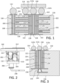
- FIG. 1 illustrates an embodiment of a via-in-via vertical interconnect.
- a conventional via vertical interconnect 104 is also illustrated for comparison.
- the conventional via vertical interconnect 104 is formed by drilling a hole through a PCB 102. Next a copper layer is plated in the hole to form a conductive vertical cylinder (or via) 106 and a via pad 110. Then the plated hole may be filled with via filling polymer 108. Then a solder ball 112 may be soldered to the via pad 110 to facilitate a connection to another device.
- These conventional via vertical interconnects 104 pass through internal layers connecting only to those required to complete the circuit.
- the PCB 102 include a variety of ground layers 116. Some of these ground layers 116 are near the via 106 and these ground layers 116 cause variations in the impedance of the conventional via vertical interconnect 104 as the signal travels through said via. As described above, as the speed of the signals increase to 112 Gbps or even 224 Gbps, these variations in the impedance of the conventional via vertical interconnect 104 start to cause problems with the integrity of the high speed signals.
- a via-in-via vertical interconnect 120 is also illustrated in FIG. 1 .
- the via-in-via vertical interconnect 120 includes an inner plated cylinder inside an outer plated ground cylinder.
- the outer ground cylinder shields the inner cylinder from the effects of the ground layers 116 while also providing a consistent reference surface.
- the via-in-via vertical interconnect 120 is formed by first drilling a hole in the PCB 102. Then the hole is plated with a copper to form an outer conductive cylinder 122 and a via-in-via ground pad 132. Next, the plated hole is filled with polymer filler 124. It is noted that the filler material may be any non-conductive filler material. Next a second hole is drilled through the polymer filler 124.
- this second hole will generally be along and generally centered in the first hole.
- the second hole is plated with a copper to form an inner conductive cylinder.
- the plated second hole is filled with polymer filler 128.
- an additional copper layer may be plated at the ends of the via-in-via vertical interconnect 120 to form the via-in-via pad 130 that is connected to the inner layer 126.
- An integrated circuit (IC) 114 may be attached to the via-in-via vertical interconnect 120 using solder balls 112.
- One solder ball 112a may be connected to the via-in-via pad 130 and two solder balls 112b are connected to the via-in-via ground pad 132. This means that the IC 114 will see a constant impedance along the inner connection of the via-in-via vertical interconnect 120 formed by the inner cylinder 126 because the inner cylinder 126 is shielded by the outer ground cylinder 122.
- FIG. 2 illustrates a coaxial cable 208 connected to the PCB 102.
- High speed signals may be connected to the PCB 102 by a coaxial cable 208 via a coaxial connector 206.
- the coaxial connector 206 may be connected to a connector board 204.
- a PCB connector 202 may then connect the connector board 204 to the PCB 102 using solder balls 112.
- the high speed signals from the coaxial cable 208 may then pass through the PCB 102 using the via-in-via vertical interconnect 120 (not shown in FIG. 2 ).
- FIG. 1 illustrates the use of the via-in-via vertical interconnect 120 to pass a signal from one side of the PCB 102 to the other.
- FIG. 3 illustrates how a signal from the top of the PCB 102 may be connected to an internal layer of the PCB 102 using a via-in-via vertical connection.
- the via-in-via vertical interconnect 220 includes an outer cylinder 222, outer filler 224, inner cylinder 226, inner filler 228, and via-in-via pad 230 like the via-in-via vertical interconnect 120.
- the lower via-in-via pad 230 ends at a via-in-via pad 230 internal to the PCB 102 at a first layer.
- This via-in-via pad 230 may then be connected to a second layer 234 using a microvia 232.
- the signal on the second layer 234 may then be transmitted to some other part of the PCB 102.
- the via-in-via vertical interconnect 220 may just be connected to the first layer.
- FIG. 4 illustrates the use of two via-in-via vertical interconnects 220 to provide a connection between two locations on the upper surface of the PCB 102.
- Each of the via-in-via vertical interconnects 220 are connected to an internal layer 238 so that a high speed signal may pass from one via-in-via vertical interconnect 220 to the other.
- the via-in-via vertical interconnects 220 may be connected directly to the internal layer 238 or may be connected using a microvia as illustrated in FIG. 3 .
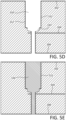
- FIGs. 5A-5K illustrate the various steps carried out to manufacture an alternate variant of via-in-via vertical interconnect 220.
- a first hole 508 is drilled through the PCB 102 with a top layer 502, internal layer 504, and bottom layer 506.
- the first hole 508 passes through internal layer 504.
- FIG. 5B illustrates the drilling of a second hole 510 into the PCB that extends to just above the internal layer 504.
- the bottom of the second hole is above the internal layer 504.
- the second hole 510 will generally be along and centered around the first hole 508.
- the diameter of the second hole 510 is larger than the diameter of the first hole 508.
- the second hole 510 and first hole 508 are plated using copper or some other conductive material as illustrated in FIG.
- a third hole 514 is drilled in the PCB 102 as illustrated in FIG. 5D .
- the third hole 514 will generally be along and centered in the second hole 510.
- the third hole 514 has a diameter larger than the diameter of first hole 508 and smaller than the diameter of the second hole 510.
- This third hole 514 is shallow and only removes a portion of the plating 512 between the first hole 508 and the second hole 510 to effectively remove the connection between the conductive plating of the second hole 510 and the first hole 508.
- the bottom of the third hole is above the internal layer 504.
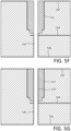
- the first hole 508, second hole 510, and third hole 514 are filled with polymer filler 516 as illustrated in FIG. 5E .
- the third hole 514 is generally along and centered in the first hole 508.
- a fourth hole 518 is drilled through the polymer filler 516 and the PCB 102 as illustrated inf FIG. 5F .
- the fourth hole 518 is generally along and centered in the second hole 510.
- the drilling of the fourth hole 518 removes the plating from the first hole 508.
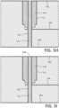
- the fourth hole 518 is plated with a copper or other conductive layer to form the inner layer 520 as illustrated in FIG. 5G .
- the plated fourth hole 518 is then filled with polymer filler 522 as illustrated in FIG. 5H .
- a copper or other connective layer is plated over the inner filler 522 to form a top pad layer 524 as illustrated in FIG. 5I .
- top pad layer 524 and top layer 502 are etched to form top layer openings 526 and top via-in-via pad 528 as illustrated in FIG. 5J .
- a fifth hole 530 is drilled from the bottom for the PCB 102 as illustrated inf FIG. 5K .
- the fifth hole 530 removes a portion of the remaining plated fourth hole 518 so that the inner layer 520 is not connected to the bottom layer 506.
- the fifth hole 530 is generally along and centered around the fourth hole 518. This manufacturing process results in a via-in-via vertical interconnect that connects a top via-in-via pad 528 to an internal layer 504 in the PCB 102.
- a signal presented at the surface of pad 520 is free to travel down the plated via 522 without loss of reference to the ground shield provided by the plating 512 of the outer hole 510 until it reaches the desired internal layer connection point 504. Without the protection afforded by the outer ground shield plating 512, the signal would experience fluctuations in impedance as it passed through surrounding ground layers and/or would experience signal corruption due to cross talk as it passed through surrounding signal layers.
- copper is used as the conductive material.
- Other types of conductive material may be used as well.
- "at least one of: a, b, or c” is intended to cover a, b, c, a-b, a-c, b-c, and a-b-c, as well as any combination with multiples of the same element (e.g., a-a, a-a-a, a-a-b, a-a-c, a-b-b, a-c-c, b-b, b-b-b, b-b-c, c-c, and c-c-c or any other ordering of a, b, and c).
Landscapes
- Engineering & Computer Science (AREA)
- Microelectronics & Electronic Packaging (AREA)
- Manufacturing & Machinery (AREA)
- Printing Elements For Providing Electric Connections Between Printed Circuits (AREA)
Abstract
A method of manufacturing a via-in-via vertical interconnect in a printed circuit board (PCB), including: drilling a first hole through the PCB and through internal conductive layer 504; drilling a second hole into a top side of the PCB; plating the first hole and the second hole with a conductive material to form an outer layer 512; drilling a third hole through the PCB wherein a portion of the plating is removed between the first hole and the second hole; filling the first, second, and third holes with an outer filler 516; drilling a fourth hole through the outer filler; plating the fourth hole with a conductive material to form an inner layer 520; filling the fourth hole with an inner filler 522; forming a via-in-via pad 528 on top of the inner filler connected to the inner layer 520; and drilling a fifth hole 530 through the bottom of the PCB along the fourth hole to remove a portion of the inner filler and inner layer wherein the top of the fifth hole is below the internal layer 504.
Description
- This application relates to vertical interconnect structures with improved impedance control and signal isolation for the purpose of higher speed signal transmission in printed circuit boards (PCB).
- Current plated through hole vertical interconnect structures used for Printed Circuit Board signal transmission introduce excessive impedance variation and opportunity for cross-talk which limit their ability to support next generation high speed signal transmission. This application relates to vertical interconnect structures with improved impedance control and signal isolation to overcome these issues.
- A summary of various exemplary embodiments is presented below.
- Various embodiments relate to a method of manufacturing a via-in-via vertical interconnect in a printed circuit board (PCB), including: drilling a first hole through the PCB and through an internal conductive layer of the PCB; drilling a second hole into a top side of the PCB around the first hole, wherein a diameter of the second hole is greater than a diameter of the first hole and a bottom of the second hole is above the internal conductive layer; plating the first hole and the second hole with a conductive material to form an outer layer; drilling a third hole through the PCB along the second hole, wherein a diameter of the third hole is less than the diameter of the second hole and is greater than the diameter of the first hole, a bottom of the third hole is above the internal conductive layer, and a portion of the plating is removed between the first hole and the second hole; filling the first, second, and third holes with a first non-conductive filler material; drilling a fourth hole through the first non-conductive filler material; plating the fourth hole with a conductive material to form an inner layer; filling the fourth hole with a second non-conductive filler material; forming a via-in-via pad on top of the second non-conductive filler connected to the inner layer.
- Various embodiments are described, wherein a fifth hole is drilled through the bottom of the PCB along the fourth hole to remove a portion of the second non-conductive filler and inner layer wherein the top of the fifth hole is below the internal conductive layer.
- Various embodiments are described, wherein forming the via-in-via pad includes plating a conductive layer over the second non-conductive filler and etching the conductive layer over the second non-conductive filler to form top layer openings and the via-in-via pad.
- Various embodiments are described, wherein the first hole is also drilled through a top conductive layer and a bottom conductive layer of the PCB.
- Further various embodiments relate to a method of manufacturing a via-in-via vertical interconnect in a printed circuit board (PCB), including: drilling a first hole through the PCB and through a top layer and a bottom layer of the PCB; plating the first hole with a conductive material to form an outer layer; filling the first hole with an outer filler; drilling a second hole through the outer filler; plating the second hole with a conductive material to form an inner layer; filling the second hole with an inner filler; and forming a via-in-via pad on top of the inner filler connected to the inner layer.
- Further various embodiments relate to a printed circuit board (PCB), including: an internal conductive layer; and a first via-in-via extending from a top surface of the PCB to the internal conductive layer, comprising: a first outer conductive layer; a first inner conductive layer inside the first outer conductive layer connected to the internal conductive layer; a first outer filler between the first outer conductive layer and the first inner conductive layer; a first inner filler inside the first inner conductive layer; and a first via-in-via pad over the first inner filler and connected to the first inner conductive layer.
- Various embodiments are described, further including: a second via-in-via extending from a surface of the PCB to the internal conductive layer, including: a second outer conductive layer; a second inner conductive layer inside the second outer conductive layer connected to the internal conductive layer; a second outer filler between the second outer conductive layer and the second inner conductive layer; a second inner filler inside the second inner conductive layer; and a second via-in-via pad over the second inner filler and connected to the second inner conductive layer, wherein the second via-in-via pad is electrically connected to the first via-in-via pad.
- Various embodiments are described, wherein the second via-in-via extends from the top surface of the PCB.
- Various embodiments are described, wherein the second via-in-via extends from a bottom surface of the PCB.
- The foregoing has outlined rather broadly the features and technical advantages of examples according to the disclosure in order that the detailed description that follows may be better understood. Additional features and advantages will be described hereinafter. The conception and specific examples disclosed may be readily utilized as a basis for modifying or designing other structures for carrying out the same purposes of the present disclosure. Such equivalent constructions do not depart from the scope of the appended claims. Characteristics of the concepts disclosed herein, both their organization and method of operation, together with associated advantages will be better understood from the following description when considered in connection with the accompanying figures. Each of the figures is provided for the purposes of illustration and description, and not as a definition of the limits of the claims.
- So that the above-recited features of the present disclosure can be understood in detail, a more particular description, briefly summarized above, may be had by reference to aspects, some of which are illustrated in the appended drawings. It is to be noted, however, that the appended drawings illustrate only certain typical aspects of this disclosure and are therefore not to be considered limiting of its scope, for the description may admit to other equally effective aspects. The same reference numbers in different drawings may identify the same or similar elements.
-
FIG. 1 illustrates an embodiment of a via-in-via vertical interconnect. -
FIG. 2 illustrates a coaxial cable connected to the PCB. -
FIG. 3 illustrates how a signal from the top of the PCB may be connected to an internal layer of the PCB using a via-in-via vertical connection. -
FIG. 4 illustrates the use of two via-in-via vertical interconnects to provide a connection between two locations on the upper surface of the PCB. -
FIGs. 5A-5K illustrate the various steps carried out to manufacture a via-in-via vertical interconnect - Various aspects of the disclosure are described more fully hereinafter with reference to the accompanying drawings. This disclosure may, however, be embodied in many different forms and should not be construed as limited to any specific structure or function presented throughout this disclosure. Rather, these aspects are provided so that this disclosure will be thorough and complete and will fully convey the scope of the disclosure to those skilled in the art. Based on the teachings herein one skilled in the art should appreciate that the scope of the disclosure is intended to cover any aspect of the disclosure disclosed herein, whether implemented independently of or combined with any other aspect of the disclosure. For example, an apparatus may be implemented or a method may be practiced using any number of the aspects set forth herein. In addition, the scope of the disclosure is intended to cover such an apparatus or method which is practiced using other structure, functionality, or structure and functionality in addition to or other than the various aspects of the disclosure set forth herein. It should be understood that any aspect of the disclosure disclosed herein may be embodied by one or more elements of a claim.
- Several aspects of via in via connections will now be presented with reference to various apparatuses and techniques. These apparatuses and techniques will be described in the following detailed description and illustrated in the accompanying drawings by various blocks, modules, components, circuits, steps, processes, algorithms, and/or the like (collectively referred to as "elements").
- Printed circuit board (PCB) technology has evolved considerably over the years to keep pace with ever increasing signal speeds. Controlled impedance, new ultra-low loss dielectrics, smoother copper foils, backdrilling of plated through holes are a few key examples of changes that have allowed boards to function properly at these higher speeds. However at its core, the PCB remains an imperfect vehicle for the transmission of high speed signals because of the way that it is made. Lamination of multiple conductive layers allows for effective isolation of signal and adequate reference to ground in the vertical axis, but in the horizontal axis, these signals must navigate around multiple structures (e.g., other signals, other vertical interconnects, and reference plane openings) each one leading to a discontinuity in the impedance of the vertical connection. At lower speeds these discontinuities were manageable, however at 112 Gbps speeds these discontinuities can be crippling, and the ability to tune the designs by adjusting for the effect of each discontinuity is becoming impossible given the density of signals and the fact that each signal must follow its own unique path. To some extent these shortcomings have been anticipated with the expectation that fiber optics would provide a path forward, however due to technical challenges, it is clear that an effective replacement to electrical signal routing at the device and PCB level is still a way off.
- Despite having evolved considerably since their introduction, the basic structure and usage of PCBs has remained fundamentally the same; photo lithography defined circuit conductors on sheets of copper foil, for the in-plane transmission of signals, with these layers being laminated together separated by dielectric separators and subsequently drilled and plated for the vertical transmission of signals. This still largely represents the state of the art. As with most electronics, miniaturization of features and tighter tolerance processes have allowed successive improvement in density and impedance control. These fundamental aspects of PCB construction limit the extent to which discontinuities in the signal's impedance may be eliminated. Some conceptual designs do anticipate routing high speed signals from chip to chip or from chip to connector without needing to go through the printed wiring board, by virtue of fiber optic links or coaxial connections at the chip substrate level, however many technical challenges remain to be resolved before this becomes a viable solution.
- Designs operating at the current maximum signal speed of 112 Gbps are showing that conventional PCB technology is truly approaching its limit. Embodiments of a via-in-via vertical interconnect are disclosed that would enable transmission of signals at 112 Gbps and even 224 Gbps without these limitations.
- To resolve the problem of numerous and excessive discontinuities encountered by high speed signals as they pass through the printed wiring board, it is necessary to extend the ground shielding to the vertical interconnect so that the signal has a stable and near continuous reference as it passes through the board. Additionally, it is important that this be accomplished using traditional multilayer printed wiring board processes so that the remainder of the printed wiring board can continue to support all of its other functions (low speed routing, power distribution, mechanical support, and the like). The via-in-via vertical interconnect provides continuous ground shielding around the signal via as it passes through the board. This via-in-via vertical interconnect may be produced using conventional fabrication processes and a process flow that still allows the printed wiring board to fulfill its other functions.
-
FIG. 1 illustrates an embodiment of a via-in-via vertical interconnect. A conventional viavertical interconnect 104 is also illustrated for comparison. - The conventional via
vertical interconnect 104 is formed by drilling a hole through aPCB 102. Next a copper layer is plated in the hole to form a conductive vertical cylinder (or via) 106 and avia pad 110. Then the plated hole may be filled with viafilling polymer 108. Then asolder ball 112 may be soldered to thevia pad 110 to facilitate a connection to another device. These conventional viavertical interconnects 104 pass through internal layers connecting only to those required to complete the circuit. - As shown in
FIG. 1 , thePCB 102 include a variety of ground layers 116. Some of these ground layers 116 are near the via 106 and these ground layers 116 cause variations in the impedance of the conventional viavertical interconnect 104 as the signal travels through said via. As described above, as the speed of the signals increase to 112 Gbps or even 224 Gbps, these variations in the impedance of the conventional viavertical interconnect 104 start to cause problems with the integrity of the high speed signals. - A via-in-via
vertical interconnect 120 is also illustrated inFIG. 1 . The via-in-viavertical interconnect 120 includes an inner plated cylinder inside an outer plated ground cylinder. The outer ground cylinder shields the inner cylinder from the effects of the ground layers 116 while also providing a consistent reference surface. Broadly, the via-in-viavertical interconnect 120 is formed by first drilling a hole in thePCB 102. Then the hole is plated with a copper to form an outerconductive cylinder 122 and a via-in-via ground pad 132. Next, the plated hole is filled withpolymer filler 124. It is noted that the filler material may be any non-conductive filler material. Next a second hole is drilled through thepolymer filler 124. Typically this second hole will generally be along and generally centered in the first hole. The second hole is plated with a copper to form an inner conductive cylinder. Then the plated second hole is filled withpolymer filler 128. Then an additional copper layer may be plated at the ends of the via-in-viavertical interconnect 120 to form the via-in-viapad 130 that is connected to theinner layer 126. - An integrated circuit (IC) 114 may be attached to the via-in-via
vertical interconnect 120 usingsolder balls 112. Onesolder ball 112a may be connected to the via-in-viapad 130 and twosolder balls 112b are connected to the via-in-via ground pad 132. This means that theIC 114 will see a constant impedance along the inner connection of the via-in-viavertical interconnect 120 formed by theinner cylinder 126 because theinner cylinder 126 is shielded by theouter ground cylinder 122. -
FIG. 2 illustrates acoaxial cable 208 connected to thePCB 102. High speed signals may be connected to thePCB 102 by acoaxial cable 208 via acoaxial connector 206. Thecoaxial connector 206 may be connected to aconnector board 204. APCB connector 202 may then connect theconnector board 204 to thePCB 102 usingsolder balls 112. The high speed signals from thecoaxial cable 208 may then pass through thePCB 102 using the via-in-via vertical interconnect 120 (not shown inFIG. 2 ). -
FIG. 1 illustrates the use of the via-in-viavertical interconnect 120 to pass a signal from one side of thePCB 102 to the other.FIG. 3 illustrates how a signal from the top of thePCB 102 may be connected to an internal layer of thePCB 102 using a via-in-via vertical connection. In this example, the via-in-viavertical interconnect 220 includes anouter cylinder 222,outer filler 224,inner cylinder 226,inner filler 228, and via-in-viapad 230 like the via-in-viavertical interconnect 120. Here the lower via-in-viapad 230 ends at a via-in-viapad 230 internal to thePCB 102 at a first layer. This via-in-viapad 230 may then be connected to asecond layer 234 using amicrovia 232. The signal on thesecond layer 234 may then be transmitted to some other part of thePCB 102. In other embodiments, the via-in-viavertical interconnect 220 may just be connected to the first layer. -
FIG. 4 illustrates the use of two via-in-viavertical interconnects 220 to provide a connection between two locations on the upper surface of thePCB 102. Each of the via-in-viavertical interconnects 220 are connected to aninternal layer 238 so that a high speed signal may pass from one via-in-viavertical interconnect 220 to the other. The via-in-viavertical interconnects 220 may be connected directly to theinternal layer 238 or may be connected using a microvia as illustrated inFIG. 3 . - .
FIGs. 5A-5K illustrate the various steps carried out to manufacture an alternate variant of via-in-viavertical interconnect 220. InFIG. 5A afirst hole 508 is drilled through thePCB 102 with atop layer 502,internal layer 504, andbottom layer 506. Thefirst hole 508 passes throughinternal layer 504. Next,FIG. 5B illustrates the drilling of asecond hole 510 into the PCB that extends to just above theinternal layer 504. The bottom of the second hole is above theinternal layer 504. Thesecond hole 510 will generally be along and centered around thefirst hole 508. The diameter of thesecond hole 510 is larger than the diameter of thefirst hole 508. Next, thesecond hole 510 andfirst hole 508 are plated using copper or some other conductive material as illustrated inFIG. 5C . Then athird hole 514 is drilled in thePCB 102 as illustrated inFIG. 5D . Thethird hole 514 will generally be along and centered in thesecond hole 510. Thethird hole 514 has a diameter larger than the diameter offirst hole 508 and smaller than the diameter of thesecond hole 510. Thisthird hole 514 is shallow and only removes a portion of theplating 512 between thefirst hole 508 and thesecond hole 510 to effectively remove the connection between the conductive plating of thesecond hole 510 and thefirst hole 508. The bottom of the third hole is above theinternal layer 504. Next, thefirst hole 508,second hole 510, andthird hole 514 are filled withpolymer filler 516 as illustrated inFIG. 5E . Thethird hole 514 is generally along and centered in thefirst hole 508. Then afourth hole 518 is drilled through thepolymer filler 516 and thePCB 102 as illustrated infFIG. 5F . Thefourth hole 518 is generally along and centered in thesecond hole 510. The drilling of thefourth hole 518 removes the plating from thefirst hole 508. Then thefourth hole 518 is plated with a copper or other conductive layer to form theinner layer 520 as illustrated inFIG. 5G . The platedfourth hole 518 is then filled withpolymer filler 522 as illustrated inFIG. 5H . Next, a copper or other connective layer is plated over theinner filler 522 to form atop pad layer 524 as illustrated inFIG. 5I . Then thetop pad layer 524 andtop layer 502 are etched to formtop layer openings 526 and top via-in-viapad 528 as illustrated inFIG. 5J . Then a fifth hole 530 is drilled from the bottom for thePCB 102 as illustrated infFIG. 5K . The fifth hole 530 removes a portion of the remaining platedfourth hole 518 so that theinner layer 520 is not connected to thebottom layer 506. The fifth hole 530 is generally along and centered around thefourth hole 518. This manufacturing process results in a via-in-via vertical interconnect that connects a top via-in-viapad 528 to aninternal layer 504 in thePCB 102. A signal presented at the surface ofpad 520 is free to travel down the plated via 522 without loss of reference to the ground shield provided by the plating 512 of theouter hole 510 until it reaches the desired internallayer connection point 504. Without the protection afforded by the outer ground shield plating 512, the signal would experience fluctuations in impedance as it passed through surrounding ground layers and/or would experience signal corruption due to cross talk as it passed through surrounding signal layers. - In the above description, copper is used as the conductive material. Other types of conductive material may be used as well.
- The foregoing disclosure provides illustration and description but is not intended to be exhaustive or to limit the aspects to the precise form disclosed. Modifications and variations may be made in light of the above disclosure or may be acquired from practice of the aspects.
- Unless stated otherwise, terms such as "first" and "second" are used to arbitrarily distinguish between the elements such terms describe. Thus, these terms are not necessarily intended to indicate temporal or other prioritization of such elements.
- While each of the embodiments are described above in terms of their structural arrangements, it should be appreciated that the aspects also cover the associated methods of using the embodiments described above.
- Even though particular combinations of features are recited in the claims and/or disclosed in the specification, these combinations are not intended to limit the disclosure of various aspects. In fact, many of these features may be combined in ways not specifically recited in the claims and/or disclosed in the specification. Although each dependent claim listed below may directly depend on only one claim, the disclosure of various aspects includes each dependent claim in combination with every other claim in the claim set. A phrase referring to "at least one of" a list of items refers to any combination of those items, including single members. As an example, "at least one of: a, b, or c" is intended to cover a, b, c, a-b, a-c, b-c, and a-b-c, as well as any combination with multiples of the same element (e.g., a-a, a-a-a, a-a-b, a-a-c, a-b-b, a-c-c, b-b, b-b-b, b-b-c, c-c, and c-c-c or any other ordering of a, b, and c).
- No element, act, or instruction used herein should be construed as critical or essential unless explicitly described as such. Also, as used herein, the articles "a" and "an" are intended to include one or more items and may be used interchangeably with "one or more." Furthermore, as used herein, the terms "set" and "group" are intended to include one or more items (e.g., related items, unrelated items, a combination of related and unrelated items, and/or the like), and may be used interchangeably with "one or more." Where only one item is intended, the phrase "only one" or similar language is used. Also, as used herein, the terms "has," "have," "having," and/or the like are intended to be open-ended terms. Further, the phrase "based on" is intended to mean "based, at least in part, on" unless explicitly stated otherwise.
Claims (8)
- A method of manufacturing a via-in-via vertical interconnect in a printed circuit board (PCB), comprising:drilling a first hole through the PCB and through an internal conductive layer of the PCB;drilling a second hole into a top side of the PCB around the first hole, wherein a diameter of the second hole is greater than a diameter of the first hole and a bottom of the second hole is above the internal conductive layer;plating the first hole and the second hole with a conductive material to form an outer layer;drilling a third hole through the PCB along the second hole, wherein a diameter of the third hole is less than the diameter of the second hole and is greater than the diameter of the first hole, a bottom of the third hole is above the internal conductive layer, and a portion of the plating is removed between the first hole and the second hole;filling the first, second, and third holes with a first non-conductive filler material;drilling a fourth hole through the first non-conductive filler material;plating the fourth hole with a conductive material to form an inner layer;filling the fourth hole with a second non-conductive filler material; andforming a via-in-via pad on top of the second non-conductive filler connected to the inner layer.
- The method of claim 1, wherein a fifth hole is drilled through the bottom of the PCB along the fourth hole to remove a portion of the second non-conductive filler and inner layer wherein the top of the fifth hole is below the internal conductive layer.
- The method of claim 1, wherein forming the via-in-via pad includesplating a conductive layer over the second non-conductive filler, andetching the conductive layer over the second non-conductive filler to form top layer openings and the via-in-via pad.
- The method of claim 1, wherein the first hole is also drilled through a top conductive layer and a bottom conductive layer of the PCB.
- A printed circuit board (PCB), comprising:an internal conductive layer; anda first via-in-via extending from a top surface of the PCB to the internal conductive layer, comprising:a first outer conductive layer;a first inner conductive layer inside the first outer conductive layer connected to the internal conductive layer;a first outer filler between the first outer conductive layer and the first inner conductive layer;a first inner filler inside the first inner conductive layer; anda first via-in-via pad over the first inner filler and connected to the first inner conductive layer.
- The PCB of claim 5, further comprising:
a second via-in-via extending from a surface of the PCB to the internal conductive layer, comprising:a second outer conductive layer;a second inner conductive layer inside the second outer conductive layer connected to the internal conductive layer;a second outer filler between the second outer conductive layer and the second inner conductive layer;a second inner filler inside the second inner conductive layer; anda second via-in-via pad over the second inner filler and connected to the second inner conductive layer, wherein the second via-in-via pad is electrically connected to the first via-in-via pad. - The PCB of claim 6, wherein the second via-in-via extends from the top surface of the PCB.
- The PCB of claim 6, wherein the second via-in-via extends from a bottom surface of the PCB.
Applications Claiming Priority (1)
| Application Number | Priority Date | Filing Date | Title |
|---|---|---|---|
| US18/354,907 US20250031318A1 (en) | 2023-07-19 | 2023-07-19 | Plated via-in-via vertical connection |
Publications (1)
| Publication Number | Publication Date |
|---|---|
| EP4496438A1 true EP4496438A1 (en) | 2025-01-22 |
Family
ID=91620796
Family Applications (1)
| Application Number | Title | Priority Date | Filing Date |
|---|---|---|---|
| EP24183474.6A Pending EP4496438A1 (en) | 2023-07-19 | 2024-06-20 | Plated via-in-via vertical connection |
Country Status (3)
| Country | Link |
|---|---|
| US (1) | US20250031318A1 (en) |
| EP (1) | EP4496438A1 (en) |
| KR (1) | KR20250015967A (en) |
Families Citing this family (1)
| Publication number | Priority date | Publication date | Assignee | Title |
|---|---|---|---|---|
| US20250365856A1 (en) * | 2024-05-21 | 2025-11-27 | R&D Circuits, Inc. (dba R&D Altanova) | Versatile high frequency monolithic multi-layered circuit board with embedded coaxial vias useful for testing of high frequency integrated circuit devices |
Citations (5)
| Publication number | Priority date | Publication date | Assignee | Title |
|---|---|---|---|---|
| US20080185180A1 (en) * | 2005-12-02 | 2008-08-07 | Cisco Technology, Inc. | Method for fabricating a printed circuit board having a coaxial via |
| US20150208514A1 (en) * | 2014-01-22 | 2015-07-23 | Sanmina Corporation | Methods of forming high aspect ratio plated through holes and high precision stub removal in a printed circuit board |
| US20150351240A1 (en) * | 2014-05-28 | 2015-12-03 | Fujitsu Limited | Print substrate, electronic device, and method of manufacturing print substrate |
| US20200178391A1 (en) * | 2017-09-14 | 2020-06-04 | Murata Manufacturing Co., Ltd. | Resin multilayer substrate and electronic device |
| US20230063808A1 (en) * | 2021-09-02 | 2023-03-02 | Apple Inc. | Coaxial via shielded interposer |
Family Cites Families (3)
| Publication number | Priority date | Publication date | Assignee | Title |
|---|---|---|---|---|
| US8227706B2 (en) * | 2008-12-31 | 2012-07-24 | Intel Corporation | Coaxial plated through holes (PTH) for robust electrical performance |
| US8354601B2 (en) * | 2010-02-25 | 2013-01-15 | Russell James V | Method and structure for coaxial via routing in printed circuit boards for improved signal integrity |
| JP5874309B2 (en) * | 2011-10-21 | 2016-03-02 | 富士通株式会社 | Wiring board and manufacturing method thereof |
-
2023
- 2023-07-19 US US18/354,907 patent/US20250031318A1/en active Pending
-
2024
- 2024-06-20 EP EP24183474.6A patent/EP4496438A1/en active Pending
- 2024-07-18 KR KR1020240095179A patent/KR20250015967A/en active Pending
Patent Citations (5)
| Publication number | Priority date | Publication date | Assignee | Title |
|---|---|---|---|---|
| US20080185180A1 (en) * | 2005-12-02 | 2008-08-07 | Cisco Technology, Inc. | Method for fabricating a printed circuit board having a coaxial via |
| US20150208514A1 (en) * | 2014-01-22 | 2015-07-23 | Sanmina Corporation | Methods of forming high aspect ratio plated through holes and high precision stub removal in a printed circuit board |
| US20150351240A1 (en) * | 2014-05-28 | 2015-12-03 | Fujitsu Limited | Print substrate, electronic device, and method of manufacturing print substrate |
| US20200178391A1 (en) * | 2017-09-14 | 2020-06-04 | Murata Manufacturing Co., Ltd. | Resin multilayer substrate and electronic device |
| US20230063808A1 (en) * | 2021-09-02 | 2023-03-02 | Apple Inc. | Coaxial via shielded interposer |
Also Published As
| Publication number | Publication date |
|---|---|
| US20250031318A1 (en) | 2025-01-23 |
| KR20250015967A (en) | 2025-02-03 |
Similar Documents
| Publication | Publication Date | Title |
|---|---|---|
| US9210809B2 (en) | Reduced PTH pad for enabling core routing and substrate layer count reduction | |
| US7402758B2 (en) | Telescoping blind via in three-layer core | |
| US10194524B1 (en) | Anti-pad for signal and power vias in printed circuit board | |
| US9202783B1 (en) | Selective antipad backdrilling for printed circuit boards | |
| TWI528871B (en) | Method and structure for coaxial via routing in printed circuit boards for improved signal integrity | |
| US6388208B1 (en) | Multi-connection via with electrically isolated segments | |
| US10292257B2 (en) | Cross-talk reduction for high speed signaling at ball grid array region and connector region | |
| US20150351219A1 (en) | Printed circuit board and method of manufacturing the same | |
| US20040149490A1 (en) | Coaxial via hole and process of fabricating the same | |
| US20100326716A1 (en) | Core via for chip package and interconnect | |
| WO2006089701A1 (en) | Air void via tuning | |
| KR20040084780A (en) | Method and apparatus for intra-layer transitions and connector launch in multilayer circuit boards | |
| US9351396B2 (en) | Printed wiring board | |
| US20250279341A1 (en) | Multilayer Cores, Variable Width Vias, and Offset Vias | |
| US7378601B2 (en) | Signal transmission structure and circuit substrate thereof | |
| KR20080014137A (en) | Design of low inductance capacitor layer connections | |
| US20060081396A1 (en) | Circuit substrate and method of manufacturing plated through slot thereon | |
| US20250031318A1 (en) | Plated via-in-via vertical connection | |
| US7088200B2 (en) | Method and structure to control common mode impedance in fan-out regions | |
| CN104472024A (en) | Apparatus and method for printed circuit boards with embedded cables | |
| TW201503775A (en) | Circuit board and manufacturing method thereof | |
| US20110011634A1 (en) | Circuit package with integrated direct-current (dc) blocking capacitor | |
| US7196906B1 (en) | Circuit board having segments with different signal speed characteristics | |
| US10917968B1 (en) | Package to printed circuit board transition | |
| JP2016081999A (en) | Circuit board and electronic device |
Legal Events
| Date | Code | Title | Description |
|---|---|---|---|
| PUAI | Public reference made under article 153(3) epc to a published international application that has entered the european phase |
Free format text: ORIGINAL CODE: 0009012 |
|
| STAA | Information on the status of an ep patent application or granted ep patent |
Free format text: STATUS: THE APPLICATION HAS BEEN PUBLISHED |
|
| AK | Designated contracting states |
Kind code of ref document: A1 Designated state(s): AL AT BE BG CH CY CZ DE DK EE ES FI FR GB GR HR HU IE IS IT LI LT LU LV MC ME MK MT NL NO PL PT RO RS SE SI SK SM TR |
|
| STAA | Information on the status of an ep patent application or granted ep patent |
Free format text: STATUS: REQUEST FOR EXAMINATION WAS MADE |
|
| 17P | Request for examination filed |
Effective date: 20250716 |