EP4496221A1 - Solid state power controller, power management system and power converter - Google Patents
Solid state power controller, power management system and power converter Download PDFInfo
- Publication number
- EP4496221A1 EP4496221A1 EP24181101.7A EP24181101A EP4496221A1 EP 4496221 A1 EP4496221 A1 EP 4496221A1 EP 24181101 A EP24181101 A EP 24181101A EP 4496221 A1 EP4496221 A1 EP 4496221A1
- Authority
- EP
- European Patent Office
- Prior art keywords
- controller
- pulsed
- voltage
- solid state
- signal
- Prior art date
- Legal status (The legal status is an assumption and is not a legal conclusion. Google has not performed a legal analysis and makes no representation as to the accuracy of the status listed.)
- Pending
Links
Images

Classifications
-
- H—ELECTRICITY
- H03—ELECTRONIC CIRCUITRY
- H03K—PULSE TECHNIQUE
- H03K17/00—Electronic switching or gating, i.e. not by contact-making and –breaking
- H03K17/08—Modifications for protecting switching circuit against overcurrent or overvoltage
- H03K17/082—Modifications for protecting switching circuit against overcurrent or overvoltage by feedback from the output to the control circuit
- H03K17/0822—Modifications for protecting switching circuit against overcurrent or overvoltage by feedback from the output to the control circuit in field-effect transistor switches
-
- H—ELECTRICITY
- H03—ELECTRONIC CIRCUITRY
- H03K—PULSE TECHNIQUE
- H03K17/00—Electronic switching or gating, i.e. not by contact-making and –breaking
- H03K17/08—Modifications for protecting switching circuit against overcurrent or overvoltage
- H03K17/082—Modifications for protecting switching circuit against overcurrent or overvoltage by feedback from the output to the control circuit
- H03K17/0828—Modifications for protecting switching circuit against overcurrent or overvoltage by feedback from the output to the control circuit in composite switches
-
- H—ELECTRICITY
- H02—GENERATION; CONVERSION OR DISTRIBUTION OF ELECTRIC POWER
- H02H—EMERGENCY PROTECTIVE CIRCUIT ARRANGEMENTS
- H02H9/00—Emergency protective circuit arrangements for limiting excess current or voltage without disconnection
- H02H9/001—Emergency protective circuit arrangements for limiting excess current or voltage without disconnection limiting speed of change of electric quantities, e.g. soft switching on or off
-
- H—ELECTRICITY
- H02—GENERATION; CONVERSION OR DISTRIBUTION OF ELECTRIC POWER
- H02H—EMERGENCY PROTECTIVE CIRCUIT ARRANGEMENTS
- H02H9/00—Emergency protective circuit arrangements for limiting excess current or voltage without disconnection
- H02H9/02—Emergency protective circuit arrangements for limiting excess current or voltage without disconnection responsive to excess current
- H02H9/025—Current limitation using field effect transistors
-
- H—ELECTRICITY
- H02—GENERATION; CONVERSION OR DISTRIBUTION OF ELECTRIC POWER
- H02M—APPARATUS FOR CONVERSION BETWEEN AC AND AC, BETWEEN AC AND DC, OR BETWEEN DC AND DC, AND FOR USE WITH MAINS OR SIMILAR POWER SUPPLY SYSTEMS; CONVERSION OF DC OR AC INPUT POWER INTO SURGE OUTPUT POWER; CONTROL OR REGULATION THEREOF
- H02M1/00—Details of apparatus for conversion
- H02M1/0045—Converters combining the concepts of switch-mode regulation and linear regulation, e.g. linear pre-regulator to switching converter, linear and switching converter in parallel, same converter or same transistor operating either in linear or switching mode
-
- H—ELECTRICITY
- H02—GENERATION; CONVERSION OR DISTRIBUTION OF ELECTRIC POWER
- H02M—APPARATUS FOR CONVERSION BETWEEN AC AND AC, BETWEEN AC AND DC, OR BETWEEN DC AND DC, AND FOR USE WITH MAINS OR SIMILAR POWER SUPPLY SYSTEMS; CONVERSION OF DC OR AC INPUT POWER INTO SURGE OUTPUT POWER; CONTROL OR REGULATION THEREOF
- H02M1/00—Details of apparatus for conversion
- H02M1/08—Circuits specially adapted for the generation of control voltages for semiconductor devices incorporated in static converters
-
- H—ELECTRICITY
- H02—GENERATION; CONVERSION OR DISTRIBUTION OF ELECTRIC POWER
- H02M—APPARATUS FOR CONVERSION BETWEEN AC AND AC, BETWEEN AC AND DC, OR BETWEEN DC AND DC, AND FOR USE WITH MAINS OR SIMILAR POWER SUPPLY SYSTEMS; CONVERSION OF DC OR AC INPUT POWER INTO SURGE OUTPUT POWER; CONTROL OR REGULATION THEREOF
- H02M1/00—Details of apparatus for conversion
- H02M1/36—Means for starting or stopping converters
-
- H—ELECTRICITY
- H03—ELECTRONIC CIRCUITRY
- H03K—PULSE TECHNIQUE
- H03K17/00—Electronic switching or gating, i.e. not by contact-making and –breaking
- H03K17/06—Modifications for ensuring a fully conducting state
-
- H—ELECTRICITY
- H03—ELECTRONIC CIRCUITRY
- H03K—PULSE TECHNIQUE
- H03K17/00—Electronic switching or gating, i.e. not by contact-making and –breaking
- H03K17/12—Modifications for increasing the maximum permissible switched current
- H03K17/122—Modifications for increasing the maximum permissible switched current in field-effect transistor switches
-
- H—ELECTRICITY
- H02—GENERATION; CONVERSION OR DISTRIBUTION OF ELECTRIC POWER
- H02M—APPARATUS FOR CONVERSION BETWEEN AC AND AC, BETWEEN AC AND DC, OR BETWEEN DC AND DC, AND FOR USE WITH MAINS OR SIMILAR POWER SUPPLY SYSTEMS; CONVERSION OF DC OR AC INPUT POWER INTO SURGE OUTPUT POWER; CONTROL OR REGULATION THEREOF
- H02M1/00—Details of apparatus for conversion
- H02M1/32—Means for protecting converters other than automatic disconnection
- H02M1/34—Snubber circuits
- H02M1/348—Passive dissipative snubbers
-
- H—ELECTRICITY
- H03—ELECTRONIC CIRCUITRY
- H03K—PULSE TECHNIQUE
- H03K2217/00—Indexing scheme related to electronic switching or gating, i.e. not by contact-making or -breaking covered by H03K17/00
- H03K2217/0027—Measuring means of, e.g. currents through or voltages across the switch
-
- H—ELECTRICITY
- H03—ELECTRONIC CIRCUITRY
- H03K—PULSE TECHNIQUE
- H03K2217/00—Indexing scheme related to electronic switching or gating, i.e. not by contact-making or -breaking covered by H03K17/00
- H03K2217/0081—Power supply means, e.g. to the switch driver
Definitions
- the present disclosure relates a solid-state power controller and a power management system as well as a power converter comprising such solid state power controller.
- apparatus and methods for switching on capacitive loads while minimizing peak inrush current are disclosed.
- capacitive loads such as load capacitor are common in a MEA or AEA distribution system.
- the connection of capacitive loads leads to inrush currents flowing through the SSPC during turn on. More particularly, during the connection of capacitive loads to a DC bus there is a high overcurrent because of zero initial energy in the capacitive loads which may cause damage to the system.
- the traditional method used with electro-mechanical switches is to have a separate pre-charge resistor during the initial period and a contactor. Different control strategies are required for the connection process by SSPCs.
- the SSPC has the DC bus and a capacitive load connected in parallel with a bleeding resistor.
- the main SSPC is comprised of a buck converter with voltage/current/temperature sensors, and a digital signal processor.
- the SSPC offers three distinct operations states ON, OFF, and a PWM current limiting.
- the ON state and OFF state disallow any current flow, whereas the PWM state allows the SSPC to gradually charge the DC load capacitor to charge gradually to avoid capacitor inrush current and over voltage spike.
- additional circuitry similar to a buck converter needs to be connected in parallel with the semiconductor device. Such additional circuitry adds weight and size to the system, which is a critical factor, e.g., in aerospace applications.
- a solid state power controller for limiting and/or breaking an electrical current flowing through a power transmission line.
- the solid state power controller comprises at least one semiconductor switch with a control terminal, a controller generating a pulsed signal, and a gate driver circuit receiving the pulsed signal generated by the controller and configured to generate a pulsed driver signal which is applied to the control terminal of the at least one semiconductor switch.
- the gate driver circuit comprises a gate driver receiving from the controller the pulsed signal and providing a pulsed output signal and driver signal generating means configured to be operable in a first state and a second state, wherein the first and second states are controlled by the controller.
- the driver signal generating means receive the gate driver pulsed output signal and are configured to generate in the first state a first pulsed driver signal which operates the at least one semiconductor switch in an active region.
- the driver signal generating means is further configured to generate in the second state a second pulsed driver signal which operates the at least one semiconductor switch in a saturated region.
- the controller is configured to set the driver signal generating means in the first state or in the second state depending on a voltage level signal received by the controller.
- aspects of the present disclosure are thus based on the idea to drive the least one semiconductor switch with a pulsed driver signal which differs in a first state and a second state, wherein the pulsed driver signal operates the at least one semiconductor switch in an active region in the first state and operates the at least one semiconductor switch in a saturated region in the second state.
- the pulsed driver signal operates the at least one semiconductor switch in an active region in the first state and operates the at least one semiconductor switch in a saturated region in the second state.
- the active region also referred as linear or non-saturation region
- the first pulsed driver signal has a lower voltage than the second pulsed driver signal.
- the controller of the solid state power controller activates the first state or the second state depending on a received voltage level signal.
- This allows the solid state power controller to, e.g., pre-charge a capacitive load as long as a received voltage level signal is below a predefined threshold, as is the case during pre-charge, before the capacitive load is fully connected to a supply voltage.
- a predefined threshold as is the case during pre-charge
- the solid state power controller may provide for further functions as known to the skilled person, such as shutting down an energy source or a load to prevent failure.
- the first state in which a first pulsed driver signal operates the at least one semiconductor switch in an active region allows for effective soft shutdown during device fault or cable fault.
- the driver generating means comprise first means receiving the pulsed output signal in the first state and generating the first pulsed driver signal and second means receiving the pulsed output signal in the second state and generating the second pulsed driver signal. Accordingly, the output of the driver circuit is applied to two different subcircuits (the first means and the second means) which provide for different voltage levels of the respective pulsed output signal. Which one of the two subcircuits is activated is controlled by the controller which, e.g., provides enable signals to the respective sub-systems.
- the first means may be implemented using a first buffer that operates under a first supply voltage.
- the second means may be implemented using a second buffer operating under a second supply voltage, wherein the first supply voltage is lower than the second supply voltage. Accordingly, the output signal of the second means has a higher voltage compared to output signal of the first means.
- a buffer within the meaning of the present disclosure is an interposed element that has a single input which is connected to the gate driver output, and a single output which is connected to the at least one semiconductor switch (typically through a resistor).
- the buffer can translate the voltage of the gate driver to the voltage needed by the semiconductor switch. The height of the translation of the voltage is defined by the supply voltage applied to the buffer.
- an RC-circuit is arranged at the input of the first buffer (and behind the gate driver). Such RC circuit smoothens the pulses received by the gate driver.
- the driver generating means comprise: a buffer receiving the pulsed output signal and generating a pulsed driver signal; and buffer output modifying means reducing the voltage level of the generated pulsed driver signal, the buffer output modifying means activatable by the controller; wherein, in the first state, the buffer output modifying means are activated, wherein the voltage level of the generated pulsed driver signal is reduced to provide the first pulsed driver signal; and wherein, in the second state, the buffer output modifying means are deactivated, wherein the generated pulsed driver signal is the second pulsed driver signal.
- the buffer output modifying means by activating or deactivating the buffer output modifying means, the first or second pulsed driver signal is provided for.
- the at least one semiconductor switch comprises a plurality of semiconductor switches arranged in parallel, each semiconductor switch comprising a control terminal to which the generated first or second pulsed driver signal is applied.
- the solid state power controller further comprises measuring means which are configured to measure the voltage over a load capacitor, wherein the measuring means generate the voltage level signal received by the controller.
- the measuring means provide a feedback to the controller.
- the measuring means may provide in particular information about the load capacitor actual charging voltage.
- the controller is configured to set the driver signal generating means in the first state (i.e., pre-charging state) if the voltage level signal received by the controller indicates that a load capacitor is charged with less than a predefined percentage of a rated voltage, and the controller is configured to set the driver signal generating means in the second state if the voltage level signal received by the controller indicates that the load capacitor is charged with more than the predefined percentage of the rated voltage.
- the at least one semiconductor switch is operated in the saturation or operating region to fully charge a load capacitor of a load such as power converters.
- the predefined percentage may be 90% of the rated voltage of the input voltage. However, other predefined percentages may be chosen as well.
- the first and second pulsed driver signals are pulse-width modulated driver signals of high-frequency, wherein high-frequency may mean to be in the range between 10 kilohertz to 100 kilohertz or higher.
- Fixed voltage pulses of controlled duration may be used in the pre-charging mode of the solid state power controller.
- a power management system comprises: a DC power supply; a load and a load capacitor; a power bus connecting the power supply and the load; the power bus comprising a solid state power controller of the first aspect; wherein the controller of the solid state power controller is configured to set the driver signal generating means in the first state in a pre-charging phase before the load is fully connected to the power supply.
- the present disclosure is applicable to all kind of load capacitor packaging technology such as aluminium electrolytic, film, compact (e.g. CERALINK TM capacitors) and ceramic capacitors.
- the high side voltage rail 3 and the low side voltage rail 4 may be formed by a busbar configuration (short: busbar).
- the busbars 3, 4 are typically made of copper or aluminum metal bars that carry large amounts of current.
- the busbars 3, 4 with mounted filtering capacitors C DC and connected to the energy supply 2 are often termed as DC link and the filtering capacitors C DC mounted on these busbars are termed as DC link capacitors which are meant to filter any AC noise present in the DC line mainly when operating at higher voltage levels.
- the SSPC 100 comprises four semiconductor switches S1 to S4, each comprising a transistor T1-T4 and a bypass diode D1-D4.
- the transistors may be MOSFET, IGBT, GaN or SiC transistors.
- the switches S1 to S4 (namely, the transistors T1-T4) are controlled by the respective gate voltage which is provided through lines 111-114 by a gate driver circuit 110.
- the diodes D1-D4 give current that flows in the opposite direction a path to flow. If the diode D1-D4 is not used, inductive current ceases instantly, generating high voltage peaks.
- the SSPC 100 further comprises a capacitor C p which has a much smaller capacity than the capacitive load C Load .
- Capacitor C p is intermittently charged by switches S1 to S4 and transfers its current to C Load during pre-charge, while this is to be understood as an example only.
- a general problem of an SSPC as shown in Figure 7 may occur in case of a soft start, when the SSPC pre-charges the load capacitor C Load , as a sudden rise of inrush current and voltage spike could not only destroy the load capacitor C Load but also destroy the switches and other connected applications.
- SSPC active pulse control solid state protection controller
- transient voltage suppressor diode 17 In parallel to the switches S11-S16 are further arranged a transient voltage suppressor diode 17 and a RC snubber sequence 18 which serve to suppress transient voltage spikes. Further, a transient voltage suppressor diode 19 is provided which is connected across the Gates G and sources of the switches S11-S16. The transient voltage suppressor diode 19 serves to suppress a transient spike in gate voltage due to its Miller capacitor charging.
- the source and drain of the switches S11-116 are connected to two DC voltages V1, V2, which may be the terminal voltages of a power supply such as in Figures 6 and 7 and/or may be voltages within a circuit.
- the semiconductor switch S1 may be the semiconductor switch S1 of the circuit of Figure 7 , in which case the voltage V1 is the voltage of the high side voltage rail 3 of Figure 7 and the voltage V2 is voltage between switches S1 and S3 of Figure 7 .
- a switch S11-S16 has three operating regions.
- a first operating region is a cut-off region, in which the switch is operating when the gate-to-source voltage is less than a threshold voltage Vth.
- the cut-off region is also known as sub-threshold region. In this region, the dependence of current on gate voltage is exponential. The magnitude of current flowing through the switch in the cut-off region is negligible as the channel is not present.
- a second operating region is the active region, also known as linear or non-saturation region.
- the active region also known as linear or non-saturation region.
- Vth threshold voltage
- a channel is formed between source and drain terminals. Now, if there is voltage difference between source and drain, current will flow. The magnitude of the current increases linearly with increasing drain voltage.
- the measurement unit 30 measures a DC link voltage across a charging capacitor C Load (such as in Figure 7 ).
- the measurement unit 30 may be implemented by a voltage sensor.
- the measurement unit 30 outputs a voltage level signal which is supplied through line 101 as input to the controller 20.
- the first buffer 12 Because of the different supply voltages, the first buffer 12 generates as output a first pulsed driver signal which operates the semiconductor switches S11-S16 in the active region.
- the second buffer 13 generates as output a second pulsed driver signal which operates the semiconductor switches S11-S16 in the saturated region. Which one of the buffers 12, 13 is used is decided by the controller 2 which provides the enable signals ENA and ENB.
- the semiconductor switches S11-S17 are operated by the controller 2 in the active region via continuous high frequency pulses, namely, the first pulsed driver signal is provided by the first buffer 12 until a load capacitor (such as load capacitor C Load of Figure 7 ) is charged up to a predefined percentage, such as 90 percent, of a rated voltage. After having reached the predefined percentage of charge, the semiconductor switches S11-D17 are operated in the saturated region (by the second pulsed driver signal provided by the second buffer 13) to fully charge the load capacitor.
- a load capacitor such as load capacitor C Load of Figure 7
- the first buffer 12 and the second buffer 13 together form a driver signal generating means which receives the gate driver pulsed output signal from the gate driver 11 and generates the pulsed driver signal.
- a driver signal generating means which receives the gate driver pulsed output signal from the gate driver 11 and generates the pulsed driver signal.
- the SSPC 1 as shown in Figure 1 may be implemented in the circuit of Figure 6 , wherein the gate driver circuit 110 is implemented by the gate driver circuit 10 of Figure 1 , and wherein all of the semiconductor switches S1 to S4 of Figure 6 can be controlled in the same manner as semiconductor switch S1 of Figure 1 .
- the SSPC 1 as shown in Figure 1 may be implemented in other circuits and configurations as well. In particular, it may be implemented in any power management system with a DC power supply.
- FIG 2 is a flowchart of the sequence of steps implemented when pre-charging a capacitive load to suppress transient current and transient voltage during start up.
- the active pulse control uses two isolated buffers 13, 12 after the gate driver 11.
- One of the buffers 12 ensures the power semiconductor switches S11-S16 active region and the other buffer 13 ensures the power semiconductor switches S11-S16 saturation region.
- the input of the gate driver 11 is enabled from the controller 20, wherein the controller 20 receives feedback from the measurement unit 30 which measures the DC link voltage across a charging capacitor.
- the first buffer 12 and the second buffer 13 together form a driver signal generating means which receives the gate driver pulsed output signal from the gate driver and generates the pulsed driver signal.
- driver signal generating means can be implemented in other manners as well.
- Figure 3 One alternative is shown in Figure 3 .
- the driver signal generating means comprise a buffer 14 which receives the pulsed output signal from the gate driver 11 on line 109. Buffer 14 generates a pulsed driver signal, which is put on line 107 through resistor R G .
- the driver signal generating means further comprise buffer output modifying means 15 which are configured to modify the voltage level of the pulsed driver signal.
- the buffer output modifying means 15 comprise a current path 110 that includes a transistor Q1 activatable by the controller 20 and a further resistor R C connected in series to the resistor R G .
- the transistor Q1 can be activated by the controller 20 through the voltage on line 108.
- the resistors R G and R C form a voltage divider for the semiconductor switches S11-S16.
- the transistor Q1 when the transistor Q1 is activated (i.e., conducts current), the voltage level of the generated pulsed driver signal is reduced. In such case, a lower first pulsed driver signal is present on line 107 such that the semiconductor switches S11-S16 are operated in the active region.
- the transistor Q1 when the transistor Q1 is deactivated (i.e., does not conduct current), the voltage level at the output of buffer 14 is not reduced such that the pulsed driver signal provided by buffer 14 is a second pulsed driver signal with a voltage level such that the semiconductor switches S11-S16 are operated in the saturated region.
- FIG. 3 may be referred to as a "voltage clamping embodiment", wherein the buffer output modifying means 15 may be referred to as “clamping means”.
- the SSPC 1 of Figure 3 may be implemented with two different pulse control methods, which are illustrated in Figures 4 and 5 .
- step 45 When the voltage V 0 reaches the threshold level, the clamping circuit / Q1 is turned off, step 45, such that the gate voltage on line 110 is transferred to the higher level making the semiconductor switches fully conductive.
- the load will tie to the circuit and end the pre-charging process, step 46. The process stops at 47.
- Figure 5 shows a variable pulse control method.
- the clamping circuit 15 is turned on by turning on transistor Q1, step 52, thereby clamping the voltage V GS to the buffer 14 output.
- a "B duty cycle” is defined in which the voltage of Q1 is clamped for 10% duration, step 53.
- the duty cycle is increased to 20 percent in a "C duty cycle”.
- the voltage V 0 over a load capacitor (such as load capacitor C Load of Figure 7 ) is monitored and compared with a threshold level which is defined to be equal or higher 95% than an input voltage Vin.
Landscapes
- Engineering & Computer Science (AREA)
- Power Engineering (AREA)
- Power Conversion In General (AREA)
Abstract
Description
- The present disclosure relates a solid-state power controller and a power management system as well as a power converter comprising such solid state power controller. Generally, apparatus and methods for switching on capacitive loads while minimizing peak inrush current are disclosed.
- There is a growing trend towards electrification of conventional aircrafts with the aim of reducing carbon emissions. A corresponding increase in voltage and power levels of more electric aircraft (MEA) and all electric aircraft (AEA) requires fast and intelligent protection circuits. The protection circuits in DC electrical systems are critical for the reliability of the system. Due to the fact that SSPCs (Solid State Power Controllers, also referred to a Solid State Protection Controllers) show a fast response time, eliminate arcing during turn-off, and have a higher reliability, SSPCs are preferred over electro-mechanical switches. SSPCs combine the functions of connecting loads to a DC bus bars and protecting electrical installations against overload and short circuits.
- One problem that has to be addressed lies in that capacitive loads such as load capacitor are common in a MEA or AEA distribution system. The connection of capacitive loads leads to inrush currents flowing through the SSPC during turn on. More particularly, during the connection of capacitive loads to a DC bus there is a high overcurrent because of zero initial energy in the capacitive loads which may cause damage to the system. The traditional method used with electro-mechanical switches is to have a separate pre-charge resistor during the initial period and a contactor. Different control strategies are required for the connection process by SSPCs.
- There is thus a need, irrespective of the concrete SSPCs configuration, to soft start charging the capacitive loads, as a sudden rise of inrush current and voltage spike could not only destroy the capacitor but may destroy the power devices and other connected applications.
- Y. Zhou, Y. Feng, T. Liu and Z. J. Shen, "A Digital-Controlled SiC-Based Solid State Circuit Breaker with Soft-Start Function for DC Microgrids," 9th IEEE International Symposium on Power Electronics for Distributed Generation Systems (PEDG), 2018, pp. 1- 7 discuss a digital controlled SSPC with soft-start up function for DC microgrids. The SSPC has the DC bus and a capacitive load connected in parallel with a bleeding resistor. The main SSPC is comprised of a buck converter with voltage/current/temperature sensors, and a digital signal processor. The SSPC offers three distinct operations states ON, OFF, and a PWM current limiting. The ON state and OFF state disallow any current flow, whereas the PWM state allows the SSPC to gradually charge the DC load capacitor to charge gradually to avoid capacitor inrush current and over voltage spike. However, additional circuitry similar to a buck converter needs to be connected in parallel with the semiconductor device. Such additional circuitry adds weight and size to the system, which is a critical factor, e.g., in aerospace applications.
- There is a need to provide a solid state power controller for pre-charging/soft starting a capacitive load when connecting it to a DC bus that allows to efficiently suppress inrush current and voltage spikes during start up.
- In a first aspect there is provided a solid state power controller for limiting and/or breaking an electrical current flowing through a power transmission line. The solid state power controller comprises at least one semiconductor switch with a control terminal, a controller generating a pulsed signal, and a gate driver circuit receiving the pulsed signal generated by the controller and configured to generate a pulsed driver signal which is applied to the control terminal of the at least one semiconductor switch.
- It is further provided that the gate driver circuit comprises a gate driver receiving from the controller the pulsed signal and providing a pulsed output signal and driver signal generating means configured to be operable in a first state and a second state, wherein the first and second states are controlled by the controller. The driver signal generating means receive the gate driver pulsed output signal and are configured to generate in the first state a first pulsed driver signal which operates the at least one semiconductor switch in an active region. The driver signal generating means is further configured to generate in the second state a second pulsed driver signal which operates the at least one semiconductor switch in a saturated region. The controller is configured to set the driver signal generating means in the first state or in the second state depending on a voltage level signal received by the controller.
- Aspects of the present disclosure are thus based on the idea to drive the least one semiconductor switch with a pulsed driver signal which differs in a first state and a second state, wherein the pulsed driver signal operates the at least one semiconductor switch in an active region in the first state and operates the at least one semiconductor switch in a saturated region in the second state. As a semiconductor switch such as a MOSFET operates in the active region (also referred as linear or non-saturation region) at a lower gate voltage than when operating in the saturated region, the first pulsed driver signal has a lower voltage than the second pulsed driver signal.
- The controller of the solid state power controller activates the first state or the second state depending on a received voltage level signal. This allows the solid state power controller to, e.g., pre-charge a capacitive load as long as a received voltage level signal is below a predefined threshold, as is the case during pre-charge, before the capacitive load is fully connected to a supply voltage. In this respect, it is to be noted that by operating a semiconductor switch in an active region parts of the voltage applied across the semiconductor switch is naturally blocked. By further using a pulsed driver signal a sharp rise of inrush current is also prevented.
- After pre-charging, the controller of the solid-state power controller activates the second state in which the at least one semiconductor switch is operated in a saturated region.
- Accordingly, the present disclosure allows to supress inrush currents and voltages during pre-charging, utilizing at least one semiconductor switch operated in the active region to charge a capacitive load.
- A further advantage associated with the present disclosure lies in that a generalized approach is provided for that can be used with any off the shelf COTs gate drivers (COT = (Commercial Off-The-Shelf). Also, the present disclosure does not require additional passive components or a device safe operating area characteristics curve. Irrespective of system operating condition and load profiles, the present disclosure is suitable to any kind of power converter application to charge a capacitor in a power system.
- It is pointed out that the solid state power controller may provide for further functions as known to the skilled person, such as shutting down an energy source or a load to prevent failure. In particular, the first state in which a first pulsed driver signal operates the at least one semiconductor switch in an active region allows for effective soft shutdown during device fault or cable fault.
- In some embodiments, the driver generating means comprise first means receiving the pulsed output signal in the first state and generating the first pulsed driver signal and second means receiving the pulsed output signal in the second state and generating the second pulsed driver signal. Accordingly, the output of the driver circuit is applied to two different subcircuits (the first means and the second means) which provide for different voltage levels of the respective pulsed output signal. Which one of the two subcircuits is activated is controlled by the controller which, e.g., provides enable signals to the respective sub-systems.
- The first means may be implemented using a first buffer that operates under a first supply voltage. The second means may be implemented using a second buffer operating under a second supply voltage, wherein the first supply voltage is lower than the second supply voltage. Accordingly, the output signal of the second means has a higher voltage compared to output signal of the first means.
- A buffer within the meaning of the present disclosure is an interposed element that has a single input which is connected to the gate driver output, and a single output which is connected to the at least one semiconductor switch (typically through a resistor). At the same time, the buffer can translate the voltage of the gate driver to the voltage needed by the semiconductor switch. The height of the translation of the voltage is defined by the supply voltage applied to the buffer.
- In some embodiments, it may be provided that an RC-circuit is arranged at the input of the first buffer (and behind the gate driver). Such RC circuit smoothens the pulses received by the gate driver.
- In some embodiments, the driver generating means comprise: a buffer receiving the pulsed output signal and generating a pulsed driver signal; and buffer output modifying means reducing the voltage level of the generated pulsed driver signal, the buffer output modifying means activatable by the controller; wherein, in the first state, the buffer output modifying means are activated, wherein the voltage level of the generated pulsed driver signal is reduced to provide the first pulsed driver signal; and wherein, in the second state, the buffer output modifying means are deactivated, wherein the generated pulsed driver signal is the second pulsed driver signal.
- Accordingly, by activating or deactivating the buffer output modifying means, the first or second pulsed driver signal is provided for.
- In such embodiments, the buffer output modifying means may comprise a current path that includes a transistor activatable by the controller and a second resistor connected in series to a first resistor, the first resistor arranged between the buffer and the at least one semiconductor switch, wherein the first resistor and the second resistor form a voltage divider for the at least one semiconductor switch. However, other means for modifying the buffer output may be provided for instead.
- The at least one semiconductor switch may comprise a MOSFET, an IGBT, a GaN transistor, a SiC transistor or any other kind of transistor. The gate of such semiconductor switch is the control terminal to which the pulsed driver signal is applied. Generally, the present disclosure is applicable to all kind of power devices packaging technology such as IGBT, SiC, and GaN devices.
- In some embodiments, the at least one semiconductor switch comprises a plurality of semiconductor switches arranged in parallel, each semiconductor switch comprising a control terminal to which the generated first or second pulsed driver signal is applied. By implementing a multiple parallel device configuration, high current and high voltage applications can be provided for.
- In some embodiments, a transient voltage suppressor diode and/or an RC snubber sequence are arranged in parallel to the plurality of semiconductor switches. This serves to suppress transient voltage spikes.
- In some embodiments, the solid state power controller further comprises measuring means which are configured to measure the voltage over a load capacitor, wherein the measuring means generate the voltage level signal received by the controller. The measuring means provide a feedback to the controller. The measuring means may provide in particular information about the load capacitor actual charging voltage.
- In some embodiments, the controller is configured to set the driver signal generating means in the first state (i.e., pre-charging state) if the voltage level signal received by the controller indicates that a load capacitor is charged with less than a predefined percentage of a rated voltage, and the controller is configured to set the driver signal generating means in the second state if the voltage level signal received by the controller indicates that the load capacitor is charged with more than the predefined percentage of the rated voltage. In the second stage, the at least one semiconductor switch is operated in the saturation or operating region to fully charge a load capacitor of a load such as power converters.
- The predefined percentage may be 90% of the rated voltage of the input voltage. However, other predefined percentages may be chosen as well.
- In some embodiments, the first and second pulsed driver signals are pulse-width modulated driver signals of high-frequency, wherein high-frequency may mean to be in the range between 10 kilohertz to 100 kilohertz or higher. Fixed voltage pulses of controlled duration may be used in the pre-charging mode of the solid state power controller.
- In a second aspect there is provided a power management system. The power management system comprises: a DC power supply; a load and a load capacitor; a power bus connecting the power supply and the load; the power bus comprising a solid state power controller of the first aspect; wherein the controller of the solid state power controller is configured to set the driver signal generating means in the first state in a pre-charging phase before the load is fully connected to the power supply.
- In some embodiments, the controller of the solid state power controller is configured to set the driver signal generating means in the first state if the voltage level signal received by the controller indicates that the load capacitor is charged with less than a predefined percentage of a rated voltage.
- The present disclosure is applicable to all kind of load capacitor packaging technology such as aluminium electrolytic, film, compact (e.g. CERALINK™ capacitors) and ceramic capacitors.
- In a third aspect there is provided a power converter that comprises: a DC power supply having a DC positive terminal, a DC negative terminal and a DC voltage UB; a high side voltage rail connected to the DC positive terminal; a low side voltage rail connected to the DC negative terminal; a load capacitor arranged between the high side voltage rail and the low side voltage rail; and a power converter circuitry arranged between the high side voltage rail and the low side voltage rail, the power converter circuitry comprising semiconductor switches; wherein the high side voltage rail and/or the low side voltage rail comprise a solid state power controller of the first aspect; and wherein the controller of the solid state power controller is configured to set the driver signal generating means in the first state in a pre-charging phase before the power converter circuitry is fully connected to the power supply.
- The power converter circuitry may be an inverter circuitry. Further, the power converter may be a three phase inverter.
- The skilled person will appreciate that except where mutually exclusive, a feature or parameter described in relation to any one of the above aspects may be applied to any other aspect. Furthermore, except where mutually exclusive, any feature or parameter described herein may be applied to any aspect and/or combined with any other feature or parameter described herein.
- The present disclosure will be explained in more detail on the basis of exemplary embodiments with reference to the accompanying drawings in which:
-
Figure 1 is a first embodiment of an SSPC, the SSPC comprising two buffers generating first and second pulsed driver signals operating a semiconductor switch in an active region or in a saturated region; -
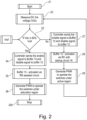
Figure 2 is a flowchart of a method used in the SSPC ofFigure 1 , the method controlling active pre-charging of a capacitive load; -
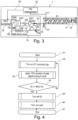
Figure 3 is a second embodiment of an SSPC, the SSPC comprising a buffer generating a pulsed driver signal and buffer output modifying means changing the voltage level of the buffer output signal, thereby providing for first and second pulsed driver signals operating a semiconductor switch in an active region or in a saturated region; -
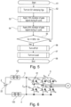
Figure 4 is a flowchart of a first method used in the SSPC ofFigure 3 , the method implementing active pre-charging of a capacitive load with constant pulse control; -
Figure 5 is a flowchart of a second method used in the SSPC ofFigure 3 , the method implementing active pre-charging of a capacitive load with variable pulse control; -
Figure 6 is a standard three-phase inverter circuit for motor drive applications comprising an SSPC; and -
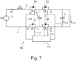
Figure 7 shows a circuit similar to the circuit ofFigure 6 with additional details regarding the SSPC. - Before discussing embodiments of the present disclosure with respect to
Figures 1 to 5 , the background of the present disclosure is discussed with respect toFigures 6 and7 to provide for a better understanding of the present disclosure. -
Figure 6 shows a standard three-phase inverter circuit for motor drive applications. The inverter circuit comprises a power supply 2 (such as a DC battery) that has apositive terminal 21 and anegative terminal 22. Between thepositive terminal 21 and the negative terminal 22 a battery voltage is present. A highside voltage rail 3 is connected to the DCpositive terminal 21 and a lowside voltage rail 4 is connected to the DCnegative terminal 22. The highside voltage rail 3 and the lowside voltage rail 4 form a high-voltage bus. - The
inverter circuit 1 further comprises a filtering capacitor CDC and an inverter circuitry 6 both arranged between the high side voltage in real 3 and the lowside voltage rail 4. The inverter circuitry 6 comprises six semiconductor power switches 61 which provide for a three-phase current U, V, W for a load M as is well known to the person skilled in the art. - The semiconductor power switches 61 each comprise a transistor S10 - S60 and a bypass diode D10-D60. The
switches 61 may be GaN (gallium nitride), SiC (silicon carbide) or IGBT (Insulated Gate Bipolar Transistor) switches. - The high
side voltage rail 3 and the lowside voltage rail 4 may be formed by a busbar configuration (short: busbar). Thebusbars busbars energy supply 2 are often termed as DC link and the filtering capacitors CDC mounted on these busbars are termed as DC link capacitors which are meant to filter any AC noise present in the DC line mainly when operating at higher voltage levels. -
Figure 6 further shows schematically that a solid state power controller 100 (in the following referred to as SSPC) is integrated both into the highside voltage rail 3 and the lowside voltage rail 4. The SSPC is bi-directional and able to isolate bothvoltage rails -
Figure 7 is similar toFigure 6 but shows more detail regarding theSSPC 100. The load is depicted in a generalized manner as RLoad, wherein RLoad may be formed, e.g., by the inverter 6 ofFigure 6 . Acapacitive load 5 is generally depicted as CLoad. It may comprise the DC link capacitors CDC ofFigure 6 and further capacitors. - The
SSPC 100 comprises four semiconductor switches S1 to S4, each comprising a transistor T1-T4 and a bypass diode D1-D4. The transistors may be MOSFET, IGBT, GaN or SiC transistors. The switches S1 to S4 (namely, the transistors T1-T4) are controlled by the respective gate voltage which is provided through lines 111-114 by agate driver circuit 110. The diodes D1-D4 give current that flows in the opposite direction a path to flow. If the diode D1-D4 is not used, inductive current ceases instantly, generating high voltage peaks. - The
SSPC 100 further comprises a capacitor Cp which has a much smaller capacity than the capacitive load CLoad. Capacitor Cp is intermittently charged by switches S1 to S4 and transfers its current to CLoad during pre-charge, while this is to be understood as an example only. - A general problem of an SSPC as shown in
Figure 7 may occur in case of a soft start, when the SSPC pre-charges the load capacitor CLoad, as a sudden rise of inrush current and voltage spike could not only destroy the load capacitor CLoad but also destroy the switches and other connected applications. To avoid this issue and suppress transient voltage and current, the present disclosure provides for an active pulse control solid state protection controller (SSPC) 1 as shown inFigure 1 . - The SSPC1 of
Figure 1 comprises a semiconductor switch S1, agate driver circuit 10, acontroller 20 and ameasurement unit 30. - The semiconductor switch S1 may be comprised of a plurality of semiconductor switches S11-S16 which are arranged in parallel, each of the switches comprising a transistor and a bypass diode as discussed with respect to
Figure 7 . Each switch S11-S16 comprises a Gate G which represents the control terminal controlling operation of the respective switch, as is well known to the skilled person. All Gates G are supplied with the same driver signal which is supplied throughline 107 by thegate driver circuit 10. The switches S11-S16 may be MOSFET, IGBT, GaN or SiC switches. By providing a plurality of switches S11-S16, a higher current can be switched. Naturally, the amount of switches S11-S16 shown inFigure 1 is exemplary only. - In parallel to the switches S11-S16 are further arranged a transient
voltage suppressor diode 17 and aRC snubber sequence 18 which serve to suppress transient voltage spikes. Further, a transientvoltage suppressor diode 19 is provided which is connected across the Gates G and sources of the switches S11-S16. The transientvoltage suppressor diode 19 serves to suppress a transient spike in gate voltage due to its Miller capacitor charging. - The source and drain of the switches S11-116 are connected to two DC voltages V1, V2, which may be the terminal voltages of a power supply such as in
Figures 6 and7 and/or may be voltages within a circuit. For example, the semiconductor switch S1 may be the semiconductor switch S1 of the circuit ofFigure 7 , in which case the voltage V1 is the voltage of the highside voltage rail 3 ofFigure 7 and the voltage V2 is voltage between switches S1 and S3 ofFigure 7 . - Because it is of relevance for the following, it is pointed out that, generally, a switch S11-S16 has three operating regions. A first operating region is a cut-off region, in which the switch is operating when the gate-to-source voltage is less than a threshold voltage Vth. The cut-off region is also known as sub-threshold region. In this region, the dependence of current on gate voltage is exponential. The magnitude of current flowing through the switch in the cut-off region is negligible as the channel is not present.
- A second operating region is the active region, also known as linear or non-saturation region. For a switch, as gate voltage increases beyond the threshold voltage Vth, a channel is formed between source and drain terminals. Now, if there is voltage difference between source and drain, current will flow. The magnitude of the current increases linearly with increasing drain voltage.
- A third operating region is the saturation region. For a switch, at a particular gate and source voltage, there is a particular level of voltage for drain, beyond which, increasing drain voltage has no effect on current. When a switch operates in this region, it is said to be in saturation.
- The
measurement unit 30 measures a DC link voltage across a charging capacitor CLoad (such as inFigure 7 ). Themeasurement unit 30 may be implemented by a voltage sensor. Themeasurement unit 30 outputs a voltage level signal which is supplied throughline 101 as input to thecontroller 20. - The
controller 20 generates a pulsed signal (such as a pulse-width modulated signal) and outputs the pulsed signal online 104. It further provides - through an isolator 17 - to enable signals ENA and ENB onlines unit 30 overline 101, as is discussed in more detail below. - The
gate driver circuit 10 comprises agate driver 11, afirst buffer 12, asecond buffer 13, theinsulator 17 and further elements Rp, Cp, RS, RG. Thegate driver 11 receives the pulsed signal fromcontroller 20 online 104 and outputs a pulsed output signal which is provided bylines buffers gate driver 11 has a positive supply voltage Vdd1 and a negative supply voltage VSS which determine the voltage of the pulsed output signal. - The pulsed driver signal is supplied on
line 106 through anRC circuit 16 that comprises a resistor Rp and a capacitor Cp to thefirst buffer 12. The pulsed driver signal is further supplied online 105 through a resistor Rs to thesecond buffer 13. - The
RC circuit 16 is connected before thefirst buffer 12 to soft-start and soft turn off the semiconductor switches S11-S16 (power devices). Theadditional RC circuit 16 after thegate driver 11 to the first (active region)buffer 12 enables the use of COTs (Commercially available gate driver), allowing expansion on higher voltage operating conditions. - The
first buffer 12 operates under a first supply voltage Vdd2, wherein thesecond buffer 13 operates under the second supply voltage Vdd1 which is the supply voltage of thegate driver 11. The first supply voltage Vdd2 is lower than the second supply voltage Vdd2. For example, Vdd2 may be in the range of 10V, while Vdd1 may be in the range of 20V. - Because of the different supply voltages, the
first buffer 12 generates as output a first pulsed driver signal which operates the semiconductor switches S11-S16 in the active region. On the other hand, thesecond buffer 13 generates as output a second pulsed driver signal which operates the semiconductor switches S11-S16 in the saturated region. Which one of thebuffers controller 2 which provides the enable signals ENA and ENB. - The semiconductor switches S11-S17 are operated by the
controller 2 in the active region via continuous high frequency pulses, namely, the first pulsed driver signal is provided by thefirst buffer 12 until a load capacitor (such as load capacitor CLoad ofFigure 7 ) is charged up to a predefined percentage, such as 90 percent, of a rated voltage. After having reached the predefined percentage of charge, the semiconductor switches S11-D17 are operated in the saturated region (by the second pulsed driver signal provided by the second buffer 13) to fully charge the load capacitor. - Once the soft start up ends, the
gate driver 11 will go back and control the second (normal region)buffer 13 to continue the operation of theSSPC 1. This secures that at no point during operation voltage spikes and transient currents go beyond the operating limit of thepower semiconductor device 1 during pre-charging conditions. - The
first buffer 12 and thesecond buffer 13 together form a driver signal generating means which receives the gate driver pulsed output signal from thegate driver 11 and generates the pulsed driver signal. By enabling thefirst buffer 12 or thesecond buffer 13 through enable signals ENA, ENB, two different states of such driver signal generating means are realized, wherein, in one state, the semiconductor switches S11-S16 are operated in the active region, and wherein, in the other state, the semiconductor switches S11-S16 are operated in the saturated region. - It is pointed out that the
SSPC 1 as shown inFigure 1 may be implemented in the circuit ofFigure 6 , wherein thegate driver circuit 110 is implemented by thegate driver circuit 10 ofFigure 1 , and wherein all of the semiconductor switches S1 to S4 ofFigure 6 can be controlled in the same manner as semiconductor switch S1 ofFigure 1 . However, this is to be understood as an example only. TheSSPC 1 as shown inFigure 1 may be implemented in other circuits and configurations as well. In particular, it may be implemented in any power management system with a DC power supply. -
Figure 2 is a flowchart of the sequence of steps implemented when pre-charging a capacitive load to suppress transient current and transient voltage during start up. As discussed with respect toFigure 1 , the active pulse control uses twoisolated buffers gate driver 11. One of thebuffers 12 ensures the power semiconductor switches S11-S16 active region and theother buffer 13 ensures the power semiconductor switches S11-S16 saturation region. The input of thegate driver 11 is enabled from thecontroller 20, wherein thecontroller 20 receives feedback from themeasurement unit 30 which measures the DC link voltage across a charging capacitor. - As can be seen in the flowchart, after
start 21, the DC link voltage Vdc is measured bymeasurement unit 30 instep 22. Thecontroller 20 receives the capacitor charging voltage information Vdc from themeasurement unit 30, and it compares with a DC link reference voltage Vref,step 23. If Vdc ≥ 90% Vref, then thecontroller 20 sends the enable signal ENA to thesecond buffer 13 and a disable signal to thefirst buffer 12,step 24. In that case, thesecond buffer 13 is activated via Rs,step 25, and a pulse width modulated driver signal (PWM) is generated to operate the semiconductor switches 11-16 in the saturation region to fully charge a load capacitor,step 26. - However, if the feedback voltage Vdc is less than the reference voltage Vref, then the
controller 20 sends an enable signal ENA to thefirst buffer 12 and a disable signal to thesecond buffer 13,step 27. In that case, thefirst buffer 12 is activated via the RCsoft start circuit 16 to suppress the transient voltage spike,step 28, and a pulse width modulated driver signal is generated to operate the semiconductor switches 11-16 in the active region to suppress inrush current of a charging capacitor. The process stops at 200. - In the embodiment shown in
Figure 1 , thefirst buffer 12 and thesecond buffer 13 together form a driver signal generating means which receives the gate driver pulsed output signal from the gate driver and generates the pulsed driver signal. Such driver signal generating means can be implemented in other manners as well. One alternative is shown inFigure 3 . - The embodiment shown in
Figure 3 is generally identical to the embodiment ofFigure 1 except for the implementation of the driver signal generating means. InFigure 3 , the driver signal generating means comprise abuffer 14 which receives the pulsed output signal from thegate driver 11 online 109.Buffer 14 generates a pulsed driver signal, which is put online 107 through resistor RG. The driver signal generating means further comprise buffer output modifying means 15 which are configured to modify the voltage level of the pulsed driver signal. - More particularly, the buffer
output modifying means 15 comprise acurrent path 110 that includes a transistor Q1 activatable by thecontroller 20 and a further resistor RC connected in series to the resistor RG. The transistor Q1 can be activated by thecontroller 20 through the voltage online 108. When current flows through transistor Q1, the resistors RG and RC form a voltage divider for the semiconductor switches S11-S16. - Accordingly, in a first state, when the transistor Q1 is activated (i.e., conducts current), the voltage level of the generated pulsed driver signal is reduced. In such case, a lower first pulsed driver signal is present on
line 107 such that the semiconductor switches S11-S16 are operated in the active region. - The other hand, when the transistor Q1 is deactivated (i.e., does not conduct current), the voltage level at the output of
buffer 14 is not reduced such that the pulsed driver signal provided bybuffer 14 is a second pulsed driver signal with a voltage level such that the semiconductor switches S11-S16 are operated in the saturated region. - The embodiment of
Figure 3 may be referred to as a "voltage clamping embodiment", wherein the bufferoutput modifying means 15 may be referred to as "clamping means". - The
SSPC 1 ofFigure 3 may be implemented with two different pulse control methods, which are illustrated inFigures 4 and5 . -
Figure 4 shows a constant pulse control method. Afterstart 41, the clampingcircuit 15 is turned on by turning on transistor Q1,step 42, thereby clamping the voltage VGS to thebuffer 14 output. An "A duty cycle" is defined in which the voltage of Q1 is clamped for 15% duration,step 43. The control signal for transistor Q1 is outputted bycontroller 20 online 108 throughisolator 170. Instep 44, the voltage V0 over a load capacitor (such as load capacitor CLoad ofFigure 7 ) is monitored and compared with a threshold level which is defined to be equal or higher 95% than an input voltage Vin. When the voltage V0 reaches the threshold level, the clamping circuit / Q1 is turned off,step 45, such that the gate voltage online 110 is transferred to the higher level making the semiconductor switches fully conductive. The load will tie to the circuit and end the pre-charging process, step 46. The process stops at 47. -
Figure 5 shows a variable pulse control method. Afterstart 51, the clampingcircuit 15 is turned on by turning on transistor Q1,step 52, thereby clamping the voltage VGS to thebuffer 14 output. A "B duty cycle" is defined in which the voltage of Q1 is clamped for 10% duration,step 53. In asubsequent step 54 the duty cycle is increased to 20 percent in a "C duty cycle". Instep 55, the voltage V0 over a load capacitor (such as load capacitor CLoad ofFigure 7 ) is monitored and compared with a threshold level which is defined to be equal or higher 95% than an input voltage Vin. When the voltage V0 reaches the threshold level, the clamping circuit / Q1 is turned off,step 56, such that the gate voltage online 110 is transferred to the higher level making the semiconductor switches fully conductive. The process stops at 58. In the method ofFigure 5 , as the duty cycle changes from B cycle to C cycle, the pulse is variable. - It should be understood that the above description is intended for illustrative purposes only, and is not intended to limit the scope of the present disclosure in any way. Also, those skilled in the art will appreciate that other aspects of the present disclosure can be obtained from a study of the drawings, the disclosure and the appended claims. All methods described herein can be performed in any suitable order unless otherwise indicated herein or otherwise clearly contradicted by context. Various features of the various embodiments disclosed herein can be combined in different combinations to create new embodiments within the scope of the present disclosure. In particular, the present disclosure extends to and includes all combinations and sub-combinations of one or more features described herein. Any ranges given herein include any and all specific values within the range and any and all sub-ranges within the given range.
Claims (16)
- A solid state power controller (1) for limiting and/or breaking an electrical current flowing through a power transmission line, the solid state power controller (1) comprising:at least one semiconductor switch (S1; S11-S16), the at least one semiconductor switch (S1; S11-S16) having a control terminal (G);a controller (20) generating a pulsed signal; anda gate driver circuit (10) receiving the pulsed signal generated by the controller (20) and configured to generate a pulsed driver signal which is applied to the control terminal (G) of the at least one semiconductor switch (S1; S11-S16);wherein the gate driver circuit (10) comprises:a gate driver (11) receiving from the controller (20) the pulsed signal and providing a pulsed output signal; anddriver signal generating means (12, 13; 14, 15) configured to be operable in a first state and a second state, the first and second states controlled by the controller (20);wherein the driver signal generating means (12, 13; 14, 15) receive the gate driver pulsed output signal and are configured to generate in the first state a first pulsed driver signal which operates the at least one semiconductor switch (S1; S11-S16) in an active region, and to generate in the second state a second pulsed driver signal which operates the at least one semiconductor switch (S1; S11-S16) in a saturated region, andwherein the controller (20) is configured to set the driver signal generating means (12, 13; 14, 15) in the first state or in the second state depending on a voltage level signal received by the controller (20).
- The solid state power controller of claim 1, wherein the driver signal generating means (12, 13) comprise:first means (12) receiving the pulsed output signal in the first state and generating the first pulsed driver signal, andsecond means (13) receiving the pulsed output signal in the second state and generating the second pulsed driver signal.
- The solid state power controller of claim 2, wherein the first means comprise a first buffer (12) operating under a first supply voltage (Vdd2) and in that the second means comprise a second buffer (13) operating under a second supply voltage (Vdd1), wherein the first supply voltage (Vdd2) is lower than the second supply voltage (Vdd1).
- The solid state power controller of claim 3, wherein an RC-circuit (16) is arranged at the input of the first buffer (12).
- The solid state power controller of claim 1, wherein the driver signal generating means (14, 15) comprise:a buffer (14) receiving the pulsed output signal and generating a pulsed driver signal; andbuffer output modifying means (15) reducing the voltage level of the generated pulsed driver signal, the buffer output modifying means (15) activatable by the controller (20);wherein, in the first state, the buffer output modifying means (15) are activated, wherein the voltage level of the generated pulsed driver signal is reduced to provide the first pulsed driver signal; andwherein, in the second state, the buffer output modifying means (15) are deactivated, wherein the generated pulsed driver signal is the second pulsed driver signal.
- The solid state power controller of claim 5, wherein the buffer output modifying means (15) comprises a current path (110) that includes a transistor (Q1) activatable by the controller (20) and a second resistor (RC) connected in series to a first resistor (RG) that is arranged between the buffer (14) and the at least one semiconductor switch (S1; S11-S16), wherein the first resistor (RG) and the second resistor (RC) form a voltage divider for the at least one semiconductor switch (S1; S11-S16).
- The solid state power controller of any preceding claim, wherein the at least one semiconductor switch (S1; S11-S16) comprises a MOSFET, an IGBT, a GaN transistor or a SiC transistor.
- The solid state power controller of any preceding claim, wherein the at least one semiconductor switch (S1; S11-S16) comprises a plurality of semiconductor switches (S11-S16) arranged in parallel, each semiconductor switch (S11-S16) comprising a control terminal (G) to which the generated first or second pulsed driver signal is applied.
- The solid state power controller of claim 8, wherein a transient voltage suppressor diode (17) and/or an RC snubber sequence (18) are arranged in parallel to the plurality of semiconductor switches (S11-S16).
- The solid state power controller of any preceding claim, wherein the solid state power controller (1) further comprises measuring means (30) which are configured to measure the voltage over a load capacitor (CLoad), wherein the measuring means (30) generate the voltage level signal received by the controller (20).
- The solid state power controller of claim 10, wherein the controller (20) is configured to set the driver signal generating means (12, 13; 14, 15) in the first state if the voltage level signal received by the controller (20) indicates that a load capacitor (CLoad) is charged with less than a predefined percentage of a rated voltage, and that the controller (20) is configured to set the driver signal generating means (12, 13; 14, 15) in the second state if the voltage level signal received by the controller (20) indicates that the load capacitor (CLoad) is charged with more than the predefined percentage of the rated voltage, optionally the predefined percentage is 90% of the rated voltage.
- The solid state power controller of any preceding claim, wherein the solid state power controller (1) is configured to provide first and second pulsed driver signals which are pulse-width modulated driver signals of high-frequency.
- A power management system comprising:a DC power supply (2);a load (RLoad) and a load capacitor (CLoad); anda power bus (3, 4) connecting the power supply (2) and the load (RLoad);wherein the power bus (3, 4) comprises a solid state power controller (1) of any preceding claim, and the controller (20) of the solid state power controller (1) is configured to set the driver signal generating means (12, 13; 14, 15) in the first state in a pre-charging phase before the load (RLoad) is fully connected to the power supply.
- The power management system of claim 13, wherein the controller (20) of the solid state power controller (1) is configured to set the driver signal generating means (12, 13; 14, 15) in the first state if the voltage level signal received by the controller (20) indicates that the load capacitor is charged with less than a predefined percentage of a rated voltage.
- A power converter comprising:a DC power supply (2) having a DC positive terminal (21), a DC negative terminal (22) and a DC voltage;a high side voltage rail (3) connected to the DC positive terminal (21);a low side voltage rail (4) connected to the DC negative terminal (22);a load capacitor (5, CLoad) arranged between the high side voltage rail (3) and the low side voltage rail (4); anda power converter circuitry (6) arranged between the high side voltage rail (3) and the low side voltage rail (4), the power converter circuitry (6) comprising semiconductor switches (61);wherein the high side voltage rail (3) and/or the low side voltage rail (4) comprise a solid state power controller (1) of any one of claims 1 to 12, andthe controller (20) of the solid state power controller (1) is configured to set the driver signal generating means (12, 13; 14, 15) in the first state in a pre-charging phase before the power converter circuitry (6) is fully connected to the power supply (2).
- The power converter of claim 15, wherein the power converter circuitry (6) is an inverter circuitry and/or a three phase inverter.
Applications Claiming Priority (1)
| Application Number | Priority Date | Filing Date | Title |
|---|---|---|---|
| GBGB2310966.3A GB202310966D0 (en) | 2023-07-18 | 2023-07-18 | Solid state power controller, power management system and power converter |
Publications (1)
| Publication Number | Publication Date |
|---|---|
| EP4496221A1 true EP4496221A1 (en) | 2025-01-22 |
Family
ID=87758409
Family Applications (1)
| Application Number | Title | Priority Date | Filing Date |
|---|---|---|---|
| EP24181101.7A Pending EP4496221A1 (en) | 2023-07-18 | 2024-06-10 | Solid state power controller, power management system and power converter |
Country Status (3)
| Country | Link |
|---|---|
| US (1) | US20250030414A1 (en) |
| EP (1) | EP4496221A1 (en) |
| GB (1) | GB202310966D0 (en) |
Citations (2)
| Publication number | Priority date | Publication date | Assignee | Title |
|---|---|---|---|---|
| US20130049686A1 (en) * | 2011-08-23 | 2013-02-28 | MAGNA E-Car Systems GmbH & Co. OG | Control circuit for limiting a load current, charging circuit and motor vehicle |
| US20140320194A1 (en) * | 2013-04-24 | 2014-10-30 | Hamilton Sundstrand Corporation | Solid state power controller gate control |
Family Cites Families (2)
| Publication number | Priority date | Publication date | Assignee | Title |
|---|---|---|---|---|
| US11374400B2 (en) * | 2020-12-01 | 2022-06-28 | Rolls-Royce Singapore Pte. Ltd. | Topology of a solid state power controller with two mid-capacitors |
| WO2022118089A1 (en) * | 2020-12-01 | 2022-06-09 | EDRIVELAB S.r.l. | Method and circuit for driving a half bridge |
-
2023
- 2023-07-18 GB GBGB2310966.3A patent/GB202310966D0/en not_active Ceased
-
2024
- 2024-06-06 US US18/736,079 patent/US20250030414A1/en active Pending
- 2024-06-10 EP EP24181101.7A patent/EP4496221A1/en active Pending
Patent Citations (2)
| Publication number | Priority date | Publication date | Assignee | Title |
|---|---|---|---|---|
| US20130049686A1 (en) * | 2011-08-23 | 2013-02-28 | MAGNA E-Car Systems GmbH & Co. OG | Control circuit for limiting a load current, charging circuit and motor vehicle |
| US20140320194A1 (en) * | 2013-04-24 | 2014-10-30 | Hamilton Sundstrand Corporation | Solid state power controller gate control |
Non-Patent Citations (3)
| Title |
|---|
| BAL SATARUPA ET AL: "Design Considerations of Bidirectional SiC Based DC Solid-State Power Controller for MEA Systems", IECON 2018 - 44TH ANNUAL CONFERENCE OF THE IEEE INDUSTRIAL ELECTRONICS SOCIETY, IEEE, 21 October 2018 (2018-10-21), pages 5745 - 5752, XP033483963, DOI: 10.1109/IECON.2018.8591242 * |
| Y. ZHOUY. FENGT. LIUZ. J. SHEN: "A Digital-Controlled SiC-Based Solid State Circuit Breaker with Soft-Start Function for DC Microgrids", IEEE INTERNATIONAL SYMPOSIUM ON POWER ELECTRONICS FOR DISTRIBUTED GENERATION SYSTEMS (PEDG),, 2018 |
| ZHOU YUANFENG ET AL: "A Digital-Controlled SiC-Based Solid State Circuit Breaker with Soft-Start Function for DC Microgrids", 2018 9TH IEEE INTERNATIONAL SYMPOSIUM ON POWER ELECTRONICS FOR DISTRIBUTED GENERATION SYSTEMS (PEDG), IEEE, 25 June 2018 (2018-06-25), pages 1 - 7, XP033395211, DOI: 10.1109/PEDG.2018.8447563 * |
Also Published As
| Publication number | Publication date |
|---|---|
| US20250030414A1 (en) | 2025-01-23 |
| GB202310966D0 (en) | 2023-08-30 |
Similar Documents
| Publication | Publication Date | Title |
|---|---|---|
| EP3219010B1 (en) | Resistor emulation and gate boost | |
| CN107070191B (en) | Device for temporarily taking over the current of an energy transmission or distribution system as required | |
| US11139808B2 (en) | Semiconductor device and power conversion system | |
| US10367407B2 (en) | Method and device for controlling a voltage-controlled power semiconductor switch that can be switched off again | |
| US10910827B2 (en) | Inrush current limiting system and method | |
| EP2980944B1 (en) | Dc power system for marine applications | |
| EP2993773A1 (en) | Bidirectional current-sense circuit | |
| CN107196546B (en) | Active discharge system of motor controller | |
| KR20250148461A (en) | Power switching device operable to reduce on-resistance and extend short circuit withstand time | |
| US11621650B2 (en) | Method for current limitation in the event of transient voltage variations at an AC output of a multi-level inverter and a multi-level inverter | |
| CN108847835B (en) | Power device driving protection circuit and control method thereof | |
| US20200251981A1 (en) | Three-level pulse width modulation technique for reducing semiconductor short circuit conduction loss | |
| Alwash et al. | Short-circuit protection of power converters with SiC current limiters | |
| US20250030414A1 (en) | Solid state power controller, power management system and power converter | |
| CN113613937A (en) | Switching device, voltage supply system, switching device operating method and manufacturing method | |
| CA2898926A1 (en) | Dc power system for marine applications | |
| CN110582930B (en) | hybrid battery | |
| EP3024143B1 (en) | Solid state power controller | |
| Takamori et al. | Adjustable current limit feature with a self-sensing and self-triggering monolithically integrated SiC circuit breaker device | |
| Velander et al. | Optimal switching of SiC lateral MOSFETs | |
| EP4109735A1 (en) | System for controlling an inductor freewheeling voltage | |
| GB2641545A (en) | DC power distribution and protection system | |
| JP2024055589A (en) | Protective Device | |
| GB2640859A (en) | A method of precharging a capacitor in a power distribution and protection system | |
| CN121727493A (en) | Optimizer, control method and photovoltaic system |
Legal Events
| Date | Code | Title | Description |
|---|---|---|---|
| PUAI | Public reference made under article 153(3) epc to a published international application that has entered the european phase |
Free format text: ORIGINAL CODE: 0009012 |
|
| STAA | Information on the status of an ep patent application or granted ep patent |
Free format text: STATUS: THE APPLICATION HAS BEEN PUBLISHED |
|
| AK | Designated contracting states |
Kind code of ref document: A1 Designated state(s): AL AT BE BG CH CY CZ DE DK EE ES FI FR GB GR HR HU IE IS IT LI LT LU LV MC ME MK MT NL NO PL PT RO RS SE SI SK SM TR |
|
| STAA | Information on the status of an ep patent application or granted ep patent |
Free format text: STATUS: REQUEST FOR EXAMINATION WAS MADE |
|
| 17P | Request for examination filed |
Effective date: 20250717 |
|
| RIC1 | Information provided on ipc code assigned before grant |
Ipc: H03K 17/082 20060101AFI20260311BHEP Ipc: H02H 9/00 20060101ALI20260311BHEP Ipc: H02H 9/02 20060101ALI20260311BHEP Ipc: H02M 1/08 20060101ALI20260311BHEP Ipc: H02M 1/36 20070101ALI20260311BHEP |
|
| GRAP | Despatch of communication of intention to grant a patent |
Free format text: ORIGINAL CODE: EPIDOSNIGR1 |
|
| STAA | Information on the status of an ep patent application or granted ep patent |
Free format text: STATUS: GRANT OF PATENT IS INTENDED |