EP4496127A1 - Antenna device - Google Patents
Antenna device Download PDFInfo
- Publication number
- EP4496127A1 EP4496127A1 EP22932350.6A EP22932350A EP4496127A1 EP 4496127 A1 EP4496127 A1 EP 4496127A1 EP 22932350 A EP22932350 A EP 22932350A EP 4496127 A1 EP4496127 A1 EP 4496127A1
- Authority
- EP
- European Patent Office
- Prior art keywords
- antenna
- component
- antenna device
- ground
- ground component
- Prior art date
- Legal status (The legal status is an assumption and is not a legal conclusion. Google has not performed a legal analysis and makes no representation as to the accuracy of the status listed.)
- Pending
Links
Images






Classifications
-
- H—ELECTRICITY
- H01—ELECTRIC ELEMENTS
- H01Q—ANTENNAS, i.e. RADIO AERIALS
- H01Q21/00—Antenna arrays or systems
- H01Q21/06—Arrays of individually energised antenna units similarly polarised and spaced apart
- H01Q21/20—Arrays of individually energised antenna units similarly polarised and spaced apart the units being spaced along or adjacent to a curvilinear path
- H01Q21/205—Arrays of individually energised antenna units similarly polarised and spaced apart the units being spaced along or adjacent to a curvilinear path providing an omnidirectional coverage
-
- H—ELECTRICITY
- H01—ELECTRIC ELEMENTS
- H01Q—ANTENNAS, i.e. RADIO AERIALS
- H01Q1/00—Details of, or arrangements associated with, antennas
- H01Q1/42—Housings not intimately mechanically associated with radiating elements, e.g. radome
-
- H—ELECTRICITY
- H01—ELECTRIC ELEMENTS
- H01Q—ANTENNAS, i.e. RADIO AERIALS
- H01Q15/00—Devices for reflection, refraction, diffraction or polarisation of waves radiated from an antenna, e.g. quasi-optical devices
- H01Q15/02—Refracting or diffracting devices, e.g. lens, prism
- H01Q15/08—Refracting or diffracting devices, e.g. lens, prism formed of solid dielectric material
-
- H—ELECTRICITY
- H01—ELECTRIC ELEMENTS
- H01Q—ANTENNAS, i.e. RADIO AERIALS
- H01Q19/00—Combinations of primary active antenna elements and units with secondary devices, e.g. with quasi-optical devices, for giving the antenna a desired directional characteristic
- H01Q19/06—Combinations of primary active antenna elements and units with secondary devices, e.g. with quasi-optical devices, for giving the antenna a desired directional characteristic using refracting or diffracting devices, e.g. lens
- H01Q19/062—Combinations of primary active antenna elements and units with secondary devices, e.g. with quasi-optical devices, for giving the antenna a desired directional characteristic using refracting or diffracting devices, e.g. lens for focusing
-
- H—ELECTRICITY
- H01—ELECTRIC ELEMENTS
- H01Q—ANTENNAS, i.e. RADIO AERIALS
- H01Q19/00—Combinations of primary active antenna elements and units with secondary devices, e.g. with quasi-optical devices, for giving the antenna a desired directional characteristic
- H01Q19/10—Combinations of primary active antenna elements and units with secondary devices, e.g. with quasi-optical devices, for giving the antenna a desired directional characteristic using reflecting surfaces
-
- H—ELECTRICITY
- H01—ELECTRIC ELEMENTS
- H01Q—ANTENNAS, i.e. RADIO AERIALS
- H01Q21/00—Antenna arrays or systems
- H01Q21/24—Combinations of antenna units polarised in different directions for transmitting or receiving circularly and elliptically polarised waves or waves linearly polarised in any direction
- H01Q21/26—Turnstile or like antennas comprising arrangements of three or more elongated elements disposed radially and symmetrically in a horizontal plane about a common centre
-
- H—ELECTRICITY
- H01—ELECTRIC ELEMENTS
- H01Q—ANTENNAS, i.e. RADIO AERIALS
- H01Q25/00—Antennas or antenna systems providing at least two radiating patterns
- H01Q25/001—Crossed polarisation dual antennas
Definitions
- the present invention relates to an antenna device.
- Non-Patent Literature 1 it has been known that in a planar structure which is made up of a first layer with one surface grounded and a dipole antenna arranged therein, and a second layer laminated on the other surface of the first layer, and in which one side of the second layer opposite the first layer is free space, and the first layer and the second layer have different relative permittivity and magnetic permeability, it is possible to improve gain under certain conditions (see, for example, Non-Patent Literature 1).
- Patent Literature 1 JP 2006-74473 A
- Non-Patent Literature 1 David R. Jackson and N. G. Alexopoulos. "Gain Enhancement Methods for Printed Circuit Antennas", IEEE transactions on antennas and propagation, September 1985, Vol.AP-33, No.9, p.976-987
- the present invention has been made with a focus on these problems and aims to provide an antenna device that can improve gain with fewer antenna elements and reduce material costs.
- Non-Patent Literature 1 the planar structure described in Non-Patent Literature 1 can provide gain improvement effects and found that by expanding the planar structure to a columnar structure and adjusting various conditions, omnidirectional property and gain improvement effects in the horizontal plane could be obtained, leading to the present invention.
- an antenna device includes a ground component made of a columnar or cylindrical conductor and connected to a ground potential; a cover component made of a material containing dielectrics, having a cylindrical shape, into which the ground component is inserted, the cover component being arranged at a distance from the ground component so as to cover an outer surface of the ground component; and an antenna element arranged between an inner surface of the cover component and the outer surface of the ground component.
- the antenna device according to the present invention can improve the gain by arranging the antenna element between the inner surface of the cover component made of a material containing dielectrics and the outer surface of the ground component connected to a ground potential and covering it with the cover component. This allows the number of antenna elements to be reduced compared to a case in which a plurality of antenna elements are arranged in a circle to obtain the same gain improvement effect. In this way, the antenna device according to the present invention can improve the gain with fewer antenna elements. In addition, by using a cover component that is less expensive than the antenna elements, the material costs of the antenna elements, the antenna feeding circuit, and the like can be reduced.
- the cover component may be made of any material that contains dielectrics and has a relative permittivity greater than 1. It is particularly preferable that the cover component be made of one type of dielectrics and have a relative permittivity of 2 to 8.
- the antenna element may be any material, but since it is arranged between the inner surface of the cover component and the outer surface of the ground component, it is preferable that it is made of a linear antenna such as a monopole antenna or a dipole antenna, or a thin antenna such as a crossed-dipole antenna.
- the antenna element is made up of a plurality of antenna elements which are arranged at equal angular intervals around a central axis of the ground component.
- the number of antenna elements is three or more.
- the antenna device may also include an element group made up of a plurality of antenna elements, in which the antenna elements are arranged at equal angular intervals around a central axis of the ground component, wherein the element group may be made up of a plurality of element groups which are arranged side by side at predetermined intervals along the central axis of the ground component.
- the element group may be made up of a plurality of element groups which are arranged side by side at predetermined intervals along the central axis of the ground component.
- excellent omnidirectional property in the horizontal plane can be realized by adjusting the number of antenna elements in each element group according to the beam width of the antenna elements.
- the antenna elements of each element group may be arranged at the same position in the circumferential direction of the central axis of the ground component.
- each antenna element of each element group is arranged at a shifted position around the central axis of the ground component with respect to a position of each antenna element of an adjacent element group. In this way, it is possible to realize even better omnidirectional property in the horizontal plane.
- ⁇ 0 is the wavelength of a used frequency in free space
- a is a distance between the inner surface of the cover component and the outer surface of the ground component.
- ⁇ g is the wavelength of a used frequency in the cover component.
- an antenna device that can improve gain with fewer antenna elements and reduce material costs.
- FIGS. 1 to 14 show an antenna device according to an embodiment of the present invention.
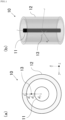
- an antenna device 10 has a ground component 11, a cover component 12, and an antenna element 13.
- the ground component 11 is made of a columnar conductor and is connected to a ground potential.
- the ground component 11 may be made of any material, such as aluminum, as long as the outer surface can be set to a ground potential.
- the ground component 11 may be cylindrical.
- the cover component 12 is cylindrical, with an inner diameter larger than the outer diameter of the ground component 11.
- the cover component 12 is made of a material containing dielectrics, and the ground component 11 is inserted inside.
- the cover component 12 is arranged coaxially with the ground component 11 at a distance from the ground component 11 so as to cover the outer surface of the ground component 11.
- the cover component 12 is made of FR4 (Flame Retardant Type 4) and has a relative permittivity of 4.3 to 5.0.
- the cover component 12 may be made of any material as long as its relative permittivity is greater than 1, but it is particularly preferable that the cover component 12 is made of one type of dielectrics and has a relative permittivity of 2 to 8.
- the antenna element 13 is arranged between the inner surface of the cover component 12 and the outer surface of the ground component 11.
- the antenna element 13 is made of a crossed-dipole antenna and is arranged so that its thickness direction is along the radial direction of the ground component 11 and the cover component 12.
- the antenna element 13 may be a linear element such as a monopole antenna or a dipole antenna, in which case it is preferable that the extension direction is parallel to the central axis of the ground component 11 and the cover component 12.
- equivalent performance may be obtained in the ranges where ⁇ 0 /4- ⁇ 0 /10 ⁇ d 1 ⁇ 0 /4+ ⁇ 0 /10, ⁇ 0 /4- ⁇ 0 /10 ⁇ d 2 ⁇ 0 /4+ ⁇ 0 /10, and ⁇ 0 /2- ⁇ 0 /10 ⁇ a ⁇ 0 /2+ ⁇ 0 /10.
- the antenna device 10 may be composed of a plurality of antenna elements 13 arranged at equal angular intervals around the central axis of the ground component 11.
- excellent omnidirectional property in the horizontal plane can be achieved by adjusting the number of antenna elements 13 according to the beam width of the antenna elements 13.
- the antenna elements 13 are arranged at the same position in the extension direction of the central axis of the ground component 11, but if the magnitude of deviation (roundness) of the gain from a circular shape in the horizontal plane deteriorates, the antenna elements 13 may be arranged at a position shifted along the central axis of the ground component 11 to improve the roundness.
- the antenna device 10 has an element group 21 made up of a plurality of antenna elements 13, in which the antenna elements 13 are arranged at equal angular intervals around the central axis of the ground component 11, and the element group 21 may be composed of a plurality of element groups which are arranged side by side at predetermined intervals h along the central axis of the ground component 11.
- the element group 21 may be composed of a plurality of element groups which are arranged side by side at predetermined intervals h along the central axis of the ground component 11.
- there are four element groups 21 in FIG. 3(a) and six element groups in FIG. 3(b) but there may be two, three, five, or seven or more element groups 21.
- the number of antenna elements 13 in each element group 21 may be any number as long as it is more than one, but it is particularly preferable that the number is three or more.
- the number of antenna elements 13 may differ for each element group 21.
- the number of antenna elements 13 in each element group 21 by adjusting the number of antenna elements 13 in each element group 21 according to the beam width of the antenna element 13, excellent omnidirectional property in the horizontal plane can be realized.
- the gain can be improved compared to when there is only one element group 21. It is preferable that the antenna elements 13 of each element group 21 are arranged at the same position in the extension direction of the central axis of the ground component 11.
- the antenna elements 13 of each element group 21 may be arranged at the same position in the circumferential direction of the central axis of the ground component 11. However, if the magnitude of deviation (roundness) of the gain from the circular shape in the horizontal plane deteriorates, the antenna elements 13 may be arranged at a shifted position around the central axis of the ground component 11 as shown in FIG. 3(d) in order to improve the roundness.
- the positions of the antenna elements 13 of adjacent element groups 21 are shifted by rotating them by 60 degrees around the central axis of the ground component 11 in order to improve the roundness.
- the antenna device 10 can improve the gain by arranging the antenna elements 13 between the inner surface of the cover component 12 made of a material containing dielectrics and the outer surface of the ground component 11 connected to the ground potential and covering it with the cover component 12. This allows the number of antenna elements 13 to be reduced compared to a case in which a plurality of antenna elements 13 are arranged in a circle to obtain the same gain improvement effect. In this way, the antenna device 10 can improve the gain with fewer antenna elements 13. In addition, by using the cover component 12, which is less expensive than the antenna elements 13, the material costs can be reduced.
- the directivity in the horizontal and vertical planes, as well as the relationship between the thickness t of the cover component 12 and the radius d 3 of the ground component 11 and the gain were obtained.
- the frequency used was 5 GHz
- the relative permittivity of the cover component 12 was 4.4.
- ⁇ 0 60 mm
- ⁇ g ⁇ 28.6 mm the relative permittivity of the cover component 12
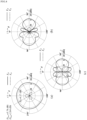
- the directivity of the antenna device 10 shown in FIG. 1 in the xy plane (horizontal plane), xz plane (vertical plane), and yz plane (vertical plane) were obtained and are shown in FIGS. 4(a) to 4(c) , respectively.
- the directivity of the antenna device 10 in the xy plane (horizontal plane), xz plane (vertical plane), and yz plane (vertical plane) were also obtained for the case where there is no cover component 12 (comparative example), and are shown in FIGS. 5(a) to 5(c) , respectively.
- the antenna element 13 is a crossed-dipole antenna, and E ⁇ and E ⁇ in each figure indicate the directivity of the horizontally polarized waves and the vertically polarized waves, respectively.
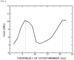
- the change in gain was obtained when the thickness t of the cover component 12 was changed for the antenna device 10 shown in FIG. 1 .
- the change in gain (Gain) with respect to the thickness t of the cover component 12 is shown in FIG. 6 .
- the change in gain was obtained when the radius d 3 of the ground component 11 was changed for the antenna device 10 shown in FIG. 1 .
- the change in gain (Gain) with respect to the radius d 3 of the ground component 11 is shown in FIG. 7 . As shown in FIG. 7 , it was confirmed that the gain increased as d 3 increased.
- the directivity in the horizontal and vertical planes were obtained for the antenna device 10 having three antenna elements 13 shown in FIG. 2 .
- the frequency used was 5 GHz
- the relative permittivity of the cover component 12 was 4.4.
- ⁇ 0 60 mm
- ⁇ g ⁇ 28.6 mm 60 mm
- the directivity in the xy plane (horizontal plane), xz plane (vertical plane), and yz plane (vertical plane) of the antenna device 10 shown in FIG. 2 were obtained and are shown in FIGS. 8(a) to 8(c) , respectively.
- the directivity in the xy plane (horizontal plane), xz plane (vertical plane), and yz plane (vertical plane) were also obtained for the case where there is no cover component 12 (comparative example), and are shown in FIGS. 9(a) to 9(c) , respectively.
- the antenna element 13 is a crossed-dipole antenna, and E ⁇ and E ⁇ in each figure indicate the directivity of horizontally polarized waves and vertically polarized waves, respectively.
- the directivity in the horizontal plane were obtained for the antenna device 10 with two element groups 21 and three antenna elements 13 in each element group 21.
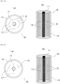
- the directivity in the horizontal plane were obtained for the antenna device 10 in which the positions of the antenna elements 13 of adjacent element groups 21 were shifted by rotating them by 60 degrees around the central axis of the ground component 11 as shown in FIG. 10 , and the antenna device 10 in which the antenna elements 13 of each element group 21 were arranged at the same position in the circumferential direction of the central axis of the ground component 11 as shown in FIG. 11 .
- ⁇ 0 60 mm
- ⁇ g ⁇ 28.6 mm were obtained for the antenna device 10 with two element groups 21 and three antenna elements 13 in each element group 21.
- the directivity in the xy plane (horizontal plane) of the antenna devices 10 shown in FIG. 10 and FIG. 11 were obtained and are shown in FIG. 12(a) and 12(b) , respectively.
- the antenna elements 13 are crossed-dipole antennas, and E ⁇ and E ⁇ in each figure indicate the directivity of horizontally polarized waves and vertically polarized waves, respectively.
- the maximum gain D max was obtained at 0 degrees and 180 degrees for the vertically polarized waves E ⁇ of the antenna device 10 of FIG. 10 .
- the maximum gain D max was obtained at 60 degrees, 180 degrees, and 300 degrees for the vertically polarized waves E ⁇ of the antenna device 10 of FIG. 11 .
- the magnitude of deviation (roundness) from a circular shape of the gain of the vertically polarized waves E ⁇ of the antenna device 10 of FIG. 10 was about 2 dB, whereas the magnitude of deviation (roundness) from a circular shape of the gain of the vertically polarized waves E ⁇ of the antenna device 10 of FIG.
- the relationship between the number of element groups 21, the interval h between the element groups 21, and the average gain was obtained from the directivity of vertically polarized waves E ⁇ in the horizontal plane.
- the number of antenna elements 13 in each element group 21 was three, and the positions of the antenna elements 13 of adjacent element groups 21 were rotated 60 degrees around the central axis of the ground component 11 and shifted.
- the frequency used was 5 GHz
- the relative permittivity of the cover component 12 was 4.4.
- ⁇ 0 60 mm
- ⁇ g ⁇ 28.6 mm 60 mm
- ⁇ g ⁇ 28.6 mm 60 mm
- the magnitude of deviation (roundness) of the gain of vertically polarized waves E ⁇ from a circular shape with respect to the number of element groups 21 when the interval h between the element groups 21 was 30 mm is shown in FIG. 13(a) .
- the roundness was 3 dB or less, and decreased to about 2 dB as the number of element groups 21 increased. From this result, it can be said that the omnidirectional property in the horizontal plane is improved by increasing the number of element groups 21.
- FIG. 13(b) The change in average gain with respect to the number of element groups 21 at this time is shown in FIG. 13(b) . As shown in FIG. 13(b) , it was confirmed that the average gain increased as the number of element groups 21 increased.
- FIG. 14(a) the magnitude of deviation (roundness) of the gain of vertically polarized waves E ⁇ from a circular shape with respect to the interval h of the element groups 21 when the number of element groups 21 was six is shown in FIG. 14(a) .
- the roundness is reduced to about 2 dB regardless of the interval h of the element groups 21, and it can be said that excellent omnidirectional property in the horizontal plane is achieved.
Landscapes
- Variable-Direction Aerials And Aerial Arrays (AREA)
- Details Of Aerials (AREA)
Abstract
Description
- The present invention relates to an antenna device.
- In general, in an antenna device used in a base station of a mobile communication system, omnidirectional property in the horizontal plane and high gain are required to support the transmission and reception of radio waves in all directions. Conventionally, in base stations and the like, a circular arrangement of a plurality of antenna elements has been widely used to achieve omnidirectional property in the horizontal plane. In addition, in order to improve gain, some circularly arranged antenna elements have been formed into an array (see, for example, Patent Literature 1).
- Note that, conventionally, it has been known that in a planar structure which is made up of a first layer with one surface grounded and a dipole antenna arranged therein, and a second layer laminated on the other surface of the first layer, and in which one side of the second layer opposite the first layer is free space, and the first layer and the second layer have different relative permittivity and magnetic permeability, it is possible to improve gain under certain conditions (see, for example, Non-Patent Literature 1).
- Patent Literature 1:
JP 2006-74473 A - Non-Patent Literature 1: David R. Jackson and N. G. Alexopoulos. "Gain Enhancement Methods for Printed Circuit Antennas", IEEE transactions on antennas and propagation, September 1985, Vol.AP-33, No.9, p.976-987
- In an antenna device in which a plurality of antenna elements are arranged in a circle, as described in Patent Literature 1, arraying a plurality of antenna elements can improve not only omnidirectional property in the horizontal plane but also the gain. However, in order to improve the gain, it is necessary to increase the number of antenna elements, which increases the material costs.
- The present invention has been made with a focus on these problems and aims to provide an antenna device that can improve gain with fewer antenna elements and reduce material costs.
- In order to achieve the above object, the inventors of the present invention conducted extensive research based on the knowledge that the planar structure described in Non-Patent Literature 1 can provide gain improvement effects and found that by expanding the planar structure to a columnar structure and adjusting various conditions, omnidirectional property and gain improvement effects in the horizontal plane could be obtained, leading to the present invention.
- That is, an antenna device according to the present invention includes a ground component made of a columnar or cylindrical conductor and connected to a ground potential; a cover component made of a material containing dielectrics, having a cylindrical shape, into which the ground component is inserted, the cover component being arranged at a distance from the ground component so as to cover an outer surface of the ground component; and an antenna element arranged between an inner surface of the cover component and the outer surface of the ground component.
- The antenna device according to the present invention can improve the gain by arranging the antenna element between the inner surface of the cover component made of a material containing dielectrics and the outer surface of the ground component connected to a ground potential and covering it with the cover component. This allows the number of antenna elements to be reduced compared to a case in which a plurality of antenna elements are arranged in a circle to obtain the same gain improvement effect. In this way, the antenna device according to the present invention can improve the gain with fewer antenna elements. In addition, by using a cover component that is less expensive than the antenna elements, the material costs of the antenna elements, the antenna feeding circuit, and the like can be reduced.
- The cover component may be made of any material that contains dielectrics and has a relative permittivity greater than 1. It is particularly preferable that the cover component be made of one type of dielectrics and have a relative permittivity of 2 to 8. The antenna element may be any material, but since it is arranged between the inner surface of the cover component and the outer surface of the ground component, it is preferable that it is made of a linear antenna such as a monopole antenna or a dipole antenna, or a thin antenna such as a crossed-dipole antenna.
- In the antenna device according to the present invention, it is preferable that the antenna element is made up of a plurality of antenna elements which are arranged at equal angular intervals around a central axis of the ground component. In this case, by adjusting the number of antenna elements according to the beam width of the antenna elements, excellent omnidirectional property in the horizontal plane can be achieved. It is particularly preferable that the number of antenna elements is three or more.
- The antenna device according to the present invention may also include an element group made up of a plurality of antenna elements, in which the antenna elements are arranged at equal angular intervals around a central axis of the ground component, wherein the element group may be made up of a plurality of element groups which are arranged side by side at predetermined intervals along the central axis of the ground component. In this case as well, excellent omnidirectional property in the horizontal plane can be realized by adjusting the number of antenna elements in each element group according to the beam width of the antenna elements. Furthermore, by using a plurality of element groups, it is possible to improve the gain compared to when there is only one element group.
- In addition, when the antenna device has a plurality of element groups, the antenna elements of each element group may be arranged at the same position in the circumferential direction of the central axis of the ground component. However, it is preferable that each antenna element of each element group is arranged at a shifted position around the central axis of the ground component with respect to a position of each antenna element of an adjacent element group. In this way, it is possible to realize even better omnidirectional property in the horizontal plane.
- In the antenna device according to the present invention, it is preferable that the cover component is arranged coaxially with the ground component, and m×0.4×λ0≤a≤m×0.6×λ0 (where m=1, 2, 3, and so on) is satisfied where λ0 is the wavelength of a used frequency in free space, and a is a distance between the inner surface of the cover component and the outer surface of the ground component. In this case, the gain improvement effect can be further improved.
- In the antenna device according to the present invention, it is preferable that each antenna element is arranged within a range of (2n-4/3)×λ0/4 to (2n-2/3)×λ0/4 (where n=1, 2, 3, and so on) from the outer surface of the ground component. In this case, the gain improvement effect can be further improved.
- In the antenna device according to the present invention, it is preferable that a thickness t of the cover component is (2q-4/3)×λg/4≤t≤(2q-2/3)×λg/4 (where q=1, 2, 3, and so on) where λg is the wavelength of a used frequency in the cover component. In this case, the gain improvement effect can be further enhanced.
- According to the present invention, it is possible to provide an antenna device that can improve gain with fewer antenna elements and reduce material costs.
-
-
FIG. 1(a) is a cross-sectional view andFIG. 1(b) is a perspective view of an antenna device according to an embodiment of the present invention. -
FIG. 2(a) is a cross-sectional view andFIG. 2(b) is a perspective view of a modified example of an antenna device according to an embodiment of the present invention, in which a plurality of antenna elements are used. -
FIG. 3 shows a modified example of an antenna device according to an embodiment of the present invention when there is a plurality of element groups, in whichFIG. 3(a) is a perspective view showing a modified example with four element groups,FIG. 3(b) is a perspective view showing a modified example with six element groups,FIG. 3(c) is a plan view showing three antenna elements of each element group arranged at the same position in the circumferential direction of the central axis of a ground component, andFIG. 3(d) is a plan view showing three antenna elements of adjacent element groups rotated 60 degrees around the central axis of the ground component. -
FIGS. 4(a), 4(b), and 4(c) show graphs showing the directivity of horizontally polarized waves Eϕ and vertically polarized waves Eθ in the xy plane (horizontal plane), the xz plane (vertical plane), and the yz plane (vertical plane) of the antenna device shown inFIG. 1 , respectively. -
FIGS. 5(a), 5(b), and 5(c) show graphs showing the directivity of horizontally polarized waves Eϕ and vertically polarized waves Eθ in the xy plane (horizontal plane), the xz plane (vertical plane), and the yz plane (vertical plane) of a comparative example without a cover component for the antenna device shown inFIG. 1 , respectively. -
FIG. 6 is a graph showing the change in maximum gain (Gain) of vertically polarized waves Eθ in the xy plane (horizontal plane) with respect to the thickness t of the cover component of the antenna device shown inFIG. 1 . -
FIG. 7 is a graph showing the change in maximum gain (Gain) of vertically polarized waves Eθ in the xy plane (horizontal plane) with respect to the radius d3 of the ground component of the antenna device shown inFIG. 1 . -
FIGS. 8(a), 8(b), and 8(c) are graphs showing the directivity of horizontally polarized waves Eϕ and vertically polarized waves Eθ in the xy plane (horizontal plane), the xz plane (vertical plane), and the yz plane (vertical plane) of the antenna device shown inFIG. 2 , respectively. -
FIGS. 9(a), 9(b), and 9(c) are graphs showing the directivity of horizontally polarized waves Eϕ and vertically polarized waves Eθ in the xy plane (horizontal plane), the xz plane (vertical plane), and the yz plane (vertical plane) of a comparative example without a cover component for the antenna device shown inFIG. 2 , respectively. -
FIG. 10(a) is a plan view andFIG. 10(b) is a perspective view of an antenna device according to an embodiment of the present invention when there are two element groups and the positions of three antenna elements of adjacent element groups are rotated 60 degrees around the central axis of the ground component. -
FIG. 11(a) is a plan view andFIG. 11(b) is a perspective view of an antenna device according to an embodiment of the present invention when there are two element groups and the three antenna elements of each element group are arranged at the same position in the circumferential direction of the central axis of the ground component. -
FIGS. 12(a) and 12(b) are graphs showing the directivity of horizontally polarized waves Eϕ and vertically polarized waves Eθ in the xy plane (horizontal plane) of the antenna device shown inFIG. 10 and the antenna device shown inFIG. 11 , respectively. -
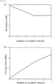
FIGS. 13(a) and 13(b) are graphs, respectively, showing the change in the magnitude of deviation (roundness) of the gain of vertically polarized waves Eθ from a circular shape and the average gain with respect to the number of element groups for the antenna devices shown inFIGS. 3(a), 3(b), and 3(d) . -
FIGS. 14(a) and 14(b) are graphs, respectively, showing the change in magnitude of deviation (roundness) of the gain of vertically polarized waves Eθ from a circular shape and the average gain with respect to the interval h between the element groups of the antenna devices shown inFIGS. 3(a), 3(b), and 3(d) . - Hereinafter, an embodiment of the present invention will be described with reference to the drawings.
-
FIGS. 1 to 14 show an antenna device according to an embodiment of the present invention. - As shown in
FIG. 1 , anantenna device 10 has aground component 11, acover component 12, and anantenna element 13. - The
ground component 11 is made of a columnar conductor and is connected to a ground potential. Theground component 11 may be made of any material, such as aluminum, as long as the outer surface can be set to a ground potential. Theground component 11 may be cylindrical. - The
cover component 12 is cylindrical, with an inner diameter larger than the outer diameter of theground component 11. Thecover component 12 is made of a material containing dielectrics, and theground component 11 is inserted inside. Thecover component 12 is arranged coaxially with theground component 11 at a distance from theground component 11 so as to cover the outer surface of theground component 11. In a specific example shown inFIG. 1 , thecover component 12 is made of FR4 (Flame Retardant Type 4) and has a relative permittivity of 4.3 to 5.0. Thecover component 12 may be made of any material as long as its relative permittivity is greater than 1, but it is particularly preferable that thecover component 12 is made of one type of dielectrics and has a relative permittivity of 2 to 8. - The
antenna element 13 is arranged between the inner surface of thecover component 12 and the outer surface of theground component 11. In a specific example shown inFIG. 1 , theantenna element 13 is made of a crossed-dipole antenna and is arranged so that its thickness direction is along the radial direction of theground component 11 and thecover component 12. Theantenna element 13 may be a linear element such as a monopole antenna or a dipole antenna, in which case it is preferable that the extension direction is parallel to the central axis of theground component 11 and thecover component 12. - As shown in
FIG. 1(a) , in one specific example of theantenna device 10, t=λg/4, d1=λ0/4, d2=λ0/4, and a=d1+d2=λ0/2, where t is the thickness of thecover component 12, a is the distance between the inner surface of thecover component 12 and the outer surface of theground component 11, d1 is the distance from the inner surface of thecover component 12 to theantenna element 13, d2 is the distance from theantenna element 13 to the outer surface of theground component 11, d3 is the radius of theground component 11, λ0 is the wavelength of the frequency used in free space, and λg is the wavelength of the frequency used in thecover component 12. In addition, equivalent performance may be obtained in the ranges where λ0/4-λ0/10≤d1≤λ0/4+λ0/10, λ0/4-λ0/10≤d2≤λ0/4+λ0/10, and λ0/2-λ0/10≤a≤λ0/2+λ0/10. - As shown in
FIG. 2 , theantenna device 10 may be composed of a plurality ofantenna elements 13 arranged at equal angular intervals around the central axis of theground component 11. In the specific example shown inFIG. 2 , there are threeantenna elements 13, but four or more antenna elements may be used. In this case, excellent omnidirectional property in the horizontal plane can be achieved by adjusting the number ofantenna elements 13 according to the beam width of theantenna elements 13. It is preferable that theantenna elements 13 are arranged at the same position in the extension direction of the central axis of theground component 11, but if the magnitude of deviation (roundness) of the gain from a circular shape in the horizontal plane deteriorates, theantenna elements 13 may be arranged at a position shifted along the central axis of theground component 11 to improve the roundness. - In addition, as shown in
FIG. 3 , theantenna device 10 has anelement group 21 made up of a plurality ofantenna elements 13, in which theantenna elements 13 are arranged at equal angular intervals around the central axis of theground component 11, and theelement group 21 may be composed of a plurality of element groups which are arranged side by side at predetermined intervals h along the central axis of theground component 11. In a specific example, there are fourelement groups 21 inFIG. 3(a) and six element groups inFIG. 3(b) , but there may be two, three, five, or seven or more element groups 21. In addition, the number ofantenna elements 13 in eachelement group 21 may be any number as long as it is more than one, but it is particularly preferable that the number is three or more. In addition, the number ofantenna elements 13 may differ for eachelement group 21. In this case as well, by adjusting the number ofantenna elements 13 in eachelement group 21 according to the beam width of theantenna element 13, excellent omnidirectional property in the horizontal plane can be realized. In addition, by using a plurality ofelement groups 21, the gain can be improved compared to when there is only oneelement group 21. It is preferable that theantenna elements 13 of eachelement group 21 are arranged at the same position in the extension direction of the central axis of theground component 11. - As shown in
FIG. 3(c) , theantenna elements 13 of eachelement group 21 may be arranged at the same position in the circumferential direction of the central axis of theground component 11. However, if the magnitude of deviation (roundness) of the gain from the circular shape in the horizontal plane deteriorates, theantenna elements 13 may be arranged at a shifted position around the central axis of theground component 11 as shown inFIG. 3(d) in order to improve the roundness. InFIGS. 3(a), 3(b) and 3(d) , the positions of theantenna elements 13 ofadjacent element groups 21 are shifted by rotating them by 60 degrees around the central axis of theground component 11 in order to improve the roundness. - Next, the operation will be described.
- The
antenna device 10 can improve the gain by arranging theantenna elements 13 between the inner surface of thecover component 12 made of a material containing dielectrics and the outer surface of theground component 11 connected to the ground potential and covering it with thecover component 12. This allows the number ofantenna elements 13 to be reduced compared to a case in which a plurality ofantenna elements 13 are arranged in a circle to obtain the same gain improvement effect. In this way, theantenna device 10 can improve the gain withfewer antenna elements 13. In addition, by using thecover component 12, which is less expensive than theantenna elements 13, the material costs can be reduced. - For the
antenna device 10 shown inFIG. 1 , the directivity in the horizontal and vertical planes, as well as the relationship between the thickness t of thecover component 12 and the radius d3 of theground component 11 and the gain were obtained. Here, the frequency used was 5 GHz, the radius of theground component 11 was d3=120 mm, and the relative permittivity of thecover component 12 was 4.4. As a result, λ0=60 mm, and λg ≈ 28.6 mm. - First, the directivity of the
antenna device 10 shown inFIG. 1 in the xy plane (horizontal plane), xz plane (vertical plane), and yz plane (vertical plane) were obtained and are shown inFIGS. 4(a) to 4(c) , respectively. For comparison, the directivity of theantenna device 10 in the xy plane (horizontal plane), xz plane (vertical plane), and yz plane (vertical plane) were also obtained for the case where there is no cover component 12 (comparative example), and are shown inFIGS. 5(a) to 5(c) , respectively. Note that theantenna element 13 is a crossed-dipole antenna, and Eϕ and Eθ in each figure indicate the directivity of the horizontally polarized waves and the vertically polarized waves, respectively. - Focusing on the vertically polarized waves Eθ in
FIG. 4(a) andFIG. 5(a) , it was confirmed that the maximum gain Dmax was obtained at 0 degrees. It was also confirmed that the maximum gain of the vertically polarized waves Eθ of theantenna device 10 inFIG. 4(a) was about 5 dB larger than that of the comparative example inFIG. 5(a) . It was also confirmed that the beam width of the vertically polarized waves Eθ of theantenna device 10 inFIG. 4(a) was slightly narrower than that of the comparative example inFIG. 5(a) . - Next, the change in gain was obtained when the thickness t of the
cover component 12 was changed for theantenna device 10 shown inFIG. 1 . The gain to be obtained was the maximum gain of the vertically polarized waves Eθ in the xy plane (horizontal plane) (gain at θ=90°, ϕ=0°). The change in gain (Gain) with respect to the thickness t of thecover component 12 is shown inFIG. 6 . As shown inFIG. 6 , it was confirmed that the gain was high near t=7.5 mm and t=22.5 mm. Here, since λg ≈ 28.6 mm, it can be said that the gain improvement effect is high when t is (2q-1)×λg/4 (where q=1, 2, 3, and so on). - Next, the change in gain was obtained when the radius d3 of the
ground component 11 was changed for theantenna device 10 shown inFIG. 1 . The gain to be obtained was the maximum gain of vertically polarized waves Eθ in the xy plane (horizontal plane) (gain at θ=90°, ϕ=0°). The change in gain (Gain) with respect to the radius d3 of theground component 11 is shown inFIG. 7 . As shown inFIG. 7 , it was confirmed that the gain increased as d3 increased. - The directivity in the horizontal and vertical planes were obtained for the
antenna device 10 having threeantenna elements 13 shown inFIG. 2 . Here, the frequency used was 5 GHz, the radius of theground component 11 was d3=8 mm, and the relative permittivity of thecover component 12 was 4.4. As a result, λ0=60 mm, and λg ≈ 28.6 mm. - The directivity in the xy plane (horizontal plane), xz plane (vertical plane), and yz plane (vertical plane) of the
antenna device 10 shown inFIG. 2 were obtained and are shown inFIGS. 8(a) to 8(c) , respectively. For comparison, the directivity in the xy plane (horizontal plane), xz plane (vertical plane), and yz plane (vertical plane) were also obtained for the case where there is no cover component 12 (comparative example), and are shown inFIGS. 9(a) to 9(c) , respectively. Note that theantenna element 13 is a crossed-dipole antenna, and Eϕ and Eθ in each figure indicate the directivity of horizontally polarized waves and vertically polarized waves, respectively. - Focusing on the vertically polarized waves Eθ in
FIGS. 8(a) and9(a) , it was confirmed that the maximum gain Dmax was obtained at 60 degrees, 180 degrees, and 300 degrees, corresponding to the positions of theantenna elements 13. It was also confirmed that the average gain of vertically polarized waves Eθ in theantenna device 10 inFIG. 8(a) was about 2 dB larger than that in the comparative example inFIG. 9(a) . It was also confirmed that the magnitude of deviation (roundness) of the gain of vertically polarized waves Eθ inFIG. 8(a) from a circular shape was within 3 dB and that the deviation from a circular shape was much smaller than that in the comparative example inFIG. 9(a) . From this result, it can be said that theantenna device 10 inFIG. 8(a) achieves excellent omnidirectional property in the horizontal plane. - The directivity in the horizontal plane were obtained for the
antenna device 10 with twoelement groups 21 and threeantenna elements 13 in eachelement group 21. Here, the directivity in the horizontal plane were obtained for theantenna device 10 in which the positions of theantenna elements 13 ofadjacent element groups 21 were shifted by rotating them by 60 degrees around the central axis of theground component 11 as shown inFIG. 10 , and theantenna device 10 in which theantenna elements 13 of eachelement group 21 were arranged at the same position in the circumferential direction of the central axis of theground component 11 as shown inFIG. 11 . The interval h between eachelement group 21 was 30 mm, the frequency used was 5 GHz, the radius of theground component 11 was d3=8 mm, and the relative permittivity of thecover component 12 was 4.4. As a result, λ0=60 mm, and λg ≈ 28.6 mm. - The directivity in the xy plane (horizontal plane) of the
antenna devices 10 shown inFIG. 10 and FIG. 11 were obtained and are shown inFIG. 12(a) and 12(b) , respectively. Note that theantenna elements 13 are crossed-dipole antennas, and Eϕ and Eθ in each figure indicate the directivity of horizontally polarized waves and vertically polarized waves, respectively. - As shown in
FIG. 12(a) , it was confirmed that the maximum gain Dmax was obtained at 0 degrees and 180 degrees for the vertically polarized waves Eθ of theantenna device 10 ofFIG. 10 . In contrast, as shown inFIG. 12(b) , it was confirmed that the maximum gain Dmax was obtained at 60 degrees, 180 degrees, and 300 degrees for the vertically polarized waves Eθ of theantenna device 10 ofFIG. 11 . In addition, the magnitude of deviation (roundness) from a circular shape of the gain of the vertically polarized waves Eθ of theantenna device 10 ofFIG. 10 was about 2 dB, whereas the magnitude of deviation (roundness) from a circular shape of the gain of the vertically polarized waves Eθ of theantenna device 10 ofFIG. 11 was about 4 dB, and it was confirmed that the magnitude of deviation from a circular shape of theantenna device 10 ofFIG. 10 was smaller than that of theantenna device 10 ofFIG. 11 . It was also confirmed that the average gain Da of the vertically polarized waves Eθ of theantenna devices 10 ofFIG. 10 and FIG. 11 was approximately the same. From these results, it can be said that in theantenna device 10 having a plurality ofelement groups 21, better omnidirectional property in the horizontal plane could be obtained by arranging theantenna elements 13 ofadjacent element groups 21 in a shifted manner around the central axis of theground component 11. - For the
antenna device 10 having a plurality ofelement groups 21 as shown inFIGS. 3(a), 3(b), and 3(d) , the relationship between the number ofelement groups 21, the interval h between theelement groups 21, and the average gain was obtained from the directivity of vertically polarized waves Eθ in the horizontal plane. Here, the number ofantenna elements 13 in eachelement group 21 was three, and the positions of theantenna elements 13 ofadjacent element groups 21 were rotated 60 degrees around the central axis of theground component 11 and shifted. In addition, the frequency used was 5 GHz, the radius of theground component 11 was d3=8 mm, and the relative permittivity of thecover component 12 was 4.4. As a result, λ0=60 mm, and λg ≈ 28.6 mm. - For the
antenna element 13 shown inFIG. 3 , the magnitude of deviation (roundness) of the gain of vertically polarized waves Eθ from a circular shape with respect to the number ofelement groups 21 when the interval h between theelement groups 21 was 30 mm is shown inFIG. 13(a) . As shown inFIG. 13(a) , it was confirmed that the roundness was 3 dB or less, and decreased to about 2 dB as the number ofelement groups 21 increased. From this result, it can be said that the omnidirectional property in the horizontal plane is improved by increasing the number of element groups 21. - The change in average gain with respect to the number of
element groups 21 at this time is shown inFIG. 13(b) . As shown inFIG. 13(b) , it was confirmed that the average gain increased as the number ofelement groups 21 increased. - Next, the magnitude of deviation (roundness) of the gain of vertically polarized waves Eθ from a circular shape with respect to the interval h of the
element groups 21 when the number ofelement groups 21 was six is shown inFIG. 14(a) . As shown inFIG. 14(a) , the roundness is reduced to about 2 dB regardless of the interval h of theelement groups 21, and it can be said that excellent omnidirectional property in the horizontal plane is achieved. - The change in average gain with respect to the interval h of the
element groups 21 in this case is shown inFIG. 14(b) . As shown inFIG. 14(b) , it was confirmed that the average gain increased as the interval h of theelement groups 21 increased. -
- 10
- Antenna device
- 11
- Ground component
- 12
- Cover component
- 13
- Antenna element
- 21
- Element group
Claims (7)
- An antenna device comprising:a ground component made of a columnar or cylindrical conductor and connected to a ground potential;a cover component made of a material containing dielectrics, having a cylindrical shape, into which the ground component is inserted, the cover component being arranged at a distance from the ground component so as to cover an outer surface of the ground component; andan antenna element arranged between an inner surface of the cover component and the outer surface of the ground component.
- The antenna device according to claim 1, wherein
the antenna element is made up of a plurality of antenna elements which are arranged at equal angular intervals around a central axis of the ground component. - The antenna device according to claim 1, further comprising:an element group made up of a plurality of antenna elements, in which the antenna elements are arranged at equal angular intervals around a central axis of the ground component, whereinthe element group is made up of a plurality of element groups which are arranged side by side at predetermined intervals along the central axis of the ground component.
- The antenna device according to claim 3, wherein
each antenna element of each element group is arranged at a shifted position around the central axis of the ground component with respect to a position of each antenna element of an adjacent element group. - The antenna device according to any one of claims 1 to 4, whereinthe cover component is arranged coaxially with the ground component, andm×0.4×λ0≤a≤m×0.6×λ0 is satisfied where λ0 is the wavelength of a used frequency in free space, a is a distance between the inner surface of the cover component and the outer surface of the ground component, and m=1, 2, 3, and so on.
- The antenna device according to claim 5, wherein
each antenna element is arranged within a range of (2n-4/3)×λ0/4 to (2n-2/3)×λ0/4, where n=1, 2, 3, and so on, from the outer surface of the ground component. - The antenna device according to any one of claims 1 to 4, wherein
a thickness t of the cover component is (2q-4/3)×λg/4≤t≤(2q-2/3)×λg/4, where λg is the wavelength of a used frequency in the cover component and q=1, 2, 3, and so on.
Applications Claiming Priority (2)
| Application Number | Priority Date | Filing Date | Title |
|---|---|---|---|
| PCT/JP2022/012896 WO2023175982A1 (en) | 2022-03-18 | 2022-03-18 | Antenna device |
| PCT/JP2022/047865 WO2023176093A1 (en) | 2022-03-18 | 2022-12-26 | Antenna device |
Publications (2)
| Publication Number | Publication Date |
|---|---|
| EP4496127A1 true EP4496127A1 (en) | 2025-01-22 |
| EP4496127A4 EP4496127A4 (en) | 2025-07-16 |
Family
ID=88023084
Family Applications (1)
| Application Number | Title | Priority Date | Filing Date |
|---|---|---|---|
| EP22932350.6A Pending EP4496127A4 (en) | 2022-03-18 | 2022-12-26 | ANTENNA DEVICE |
Country Status (6)
| Country | Link |
|---|---|
| US (1) | US20250202134A1 (en) |
| EP (1) | EP4496127A4 (en) |
| JP (1) | JP7863365B2 (en) |
| CN (1) | CN118830145A (en) |
| TW (1) | TW202339350A (en) |
| WO (2) | WO2023175982A1 (en) |
Family Cites Families (10)
| Publication number | Priority date | Publication date | Assignee | Title |
|---|---|---|---|---|
| JPS4984153A (en) * | 1972-12-15 | 1974-08-13 | ||
| JP3240568B2 (en) * | 1991-12-24 | 2001-12-17 | アイシン精機株式会社 | Multi-frequency microstrip antenna |
| JP3340271B2 (en) * | 1994-12-27 | 2002-11-05 | 株式会社東芝 | Omnidirectional antenna |
| JP4383646B2 (en) * | 2000-11-14 | 2009-12-16 | 住友電気工業株式会社 | Super turn style antenna |
| JP2005117493A (en) | 2003-10-09 | 2005-04-28 | Nippon Dengyo Kosaku Co Ltd | Frequency sharing omnidirectional antenna and array antenna |
| JP2006074473A (en) | 2004-09-02 | 2006-03-16 | Mitsubishi Electric Corp | Antenna device |
| JP2010124194A (en) * | 2008-11-19 | 2010-06-03 | Mitsubishi Electric Corp | Antenna device |
| JP5307092B2 (en) | 2010-08-18 | 2013-10-02 | シャープ株式会社 | ANTENNA DEVICE AND ELECTRIC DEVICE HAVING THE SAME |
| KR20130098098A (en) * | 2012-02-27 | 2013-09-04 | 한국전자통신연구원 | High-gain wideband antenna apparatus |
| WO2018047234A1 (en) * | 2016-09-06 | 2018-03-15 | 日本電業工作株式会社 | Antenna device and mimo communication system |
-
2022
- 2022-03-18 WO PCT/JP2022/012896 patent/WO2023175982A1/en not_active Ceased
- 2022-12-26 CN CN202280093724.8A patent/CN118830145A/en active Pending
- 2022-12-26 JP JP2024507523A patent/JP7863365B2/en active Active
- 2022-12-26 WO PCT/JP2022/047865 patent/WO2023176093A1/en not_active Ceased
- 2022-12-26 US US18/847,375 patent/US20250202134A1/en active Pending
- 2022-12-26 EP EP22932350.6A patent/EP4496127A4/en active Pending
-
2023
- 2023-02-16 TW TW112105582A patent/TW202339350A/en unknown
Also Published As
| Publication number | Publication date |
|---|---|
| EP4496127A4 (en) | 2025-07-16 |
| JPWO2023176093A1 (en) | 2023-09-21 |
| CN118830145A (en) | 2024-10-22 |
| WO2023176093A1 (en) | 2023-09-21 |
| WO2023175982A1 (en) | 2023-09-21 |
| JP7863365B2 (en) | 2026-05-21 |
| US20250202134A1 (en) | 2025-06-19 |
| TW202339350A (en) | 2023-10-01 |
Similar Documents
| Publication | Publication Date | Title |
|---|---|---|
| US8749441B2 (en) | Simultaneous transmit and receive antenna system | |
| CN109687116B (en) | C-band miniaturized broadband wide-beam circularly polarized microstrip antenna | |
| US10044111B2 (en) | Wideband dual-polarized patch antenna | |
| CN105612660B (en) | A common aperture antenna and base station | |
| US8742990B2 (en) | Circular polarization antenna | |
| US20130271336A1 (en) | Dual polarized radiating dipole antenna | |
| US20140368395A1 (en) | Crosspolar multiband panel antenna | |
| US11456544B2 (en) | Multiband antenna array with massive multiple input multiple output array | |
| US11621500B2 (en) | Circularly symmetric tightly coupled dipole array | |
| EP2905840B1 (en) | Reflect array | |
| US20230163462A1 (en) | Antenna device with improved radiation directivity | |
| WO2021226837A1 (en) | Antenna, antenna array and communication device | |
| US11145991B1 (en) | Systems and methods for phase-coincidential dual-polarized wideband antenna arrays | |
| US20210218136A1 (en) | Antenna of a terminal device | |
| US10673148B1 (en) | Circularly symmetric tightly coupled dipole array with non-coincident phase center | |
| WO2013062547A1 (en) | Simultaneous transmit and receive antenna system | |
| AU2014332522B2 (en) | Low profile high efficiency multi-band reflector antennas | |
| US20090160729A1 (en) | Antenna array with reduced electromagnetic coupling | |
| US20250202134A1 (en) | Antenna device | |
| US20240235052A9 (en) | Antenna device | |
| US7084822B2 (en) | Dual feed common radiator antenna system and method for broadcasting analog and digital signals | |
| CN120604398A (en) | Circularly polarized antenna unit and control method thereof, circularly polarized antenna and communication equipment | |
| KR101775516B1 (en) | Crpa array antenna | |
| US20250070479A1 (en) | Split sector inclined antenna reflector for improved gain | |
| Roy | Circular antenna array for direction finding applications at 2.45 ghz |
Legal Events
| Date | Code | Title | Description |
|---|---|---|---|
| STAA | Information on the status of an ep patent application or granted ep patent |
Free format text: STATUS: THE INTERNATIONAL PUBLICATION HAS BEEN MADE |
|
| PUAI | Public reference made under article 153(3) epc to a published international application that has entered the european phase |
Free format text: ORIGINAL CODE: 0009012 |
|
| STAA | Information on the status of an ep patent application or granted ep patent |
Free format text: STATUS: REQUEST FOR EXAMINATION WAS MADE |
|
| 17P | Request for examination filed |
Effective date: 20241007 |
|
| AK | Designated contracting states |
Kind code of ref document: A1 Designated state(s): AL AT BE BG CH CY CZ DE DK EE ES FI FR GB GR HR HU IE IS IT LI LT LU LV MC ME MK MT NL NO PL PT RO RS SE SI SK SM TR |
|
| DAV | Request for validation of the european patent (deleted) | ||
| DAX | Request for extension of the european patent (deleted) | ||
| A4 | Supplementary search report drawn up and despatched |
Effective date: 20250617 |
|
| RIC1 | Information provided on ipc code assigned before grant |
Ipc: H01Q 21/26 20060101AFI20250611BHEP Ipc: H01Q 1/42 20060101ALI20250611BHEP Ipc: H01Q 15/08 20060101ALI20250611BHEP Ipc: H01Q 19/06 20060101ALI20250611BHEP Ipc: H01Q 19/10 20060101ALI20250611BHEP Ipc: H01Q 19/24 20060101ALI20250611BHEP Ipc: H01Q 21/20 20060101ALI20250611BHEP Ipc: H01Q 25/00 20060101ALI20250611BHEP |