EP4496013A1 - Light-emitting device and method of manufacturing the same - Google Patents
Light-emitting device and method of manufacturing the same Download PDFInfo
- Publication number
- EP4496013A1 EP4496013A1 EP23220473.5A EP23220473A EP4496013A1 EP 4496013 A1 EP4496013 A1 EP 4496013A1 EP 23220473 A EP23220473 A EP 23220473A EP 4496013 A1 EP4496013 A1 EP 4496013A1
- Authority
- EP
- European Patent Office
- Prior art keywords
- light
- semiconductor layer
- emitting
- body portion
- base semiconductor
- Prior art date
- Legal status (The legal status is an assumption and is not a legal conclusion. Google has not performed a legal analysis and makes no representation as to the accuracy of the status listed.)
- Granted
Links
Images










Classifications
-
- H—ELECTRICITY
- H10—SEMICONDUCTOR DEVICES; ELECTRIC SOLID-STATE DEVICES NOT OTHERWISE PROVIDED FOR
- H10H—INORGANIC LIGHT-EMITTING SEMICONDUCTOR DEVICES HAVING POTENTIAL BARRIERS
- H10H20/00—Individual inorganic light-emitting semiconductor devices having potential barriers, e.g. light-emitting diodes [LED]
- H10H20/80—Constructional details
- H10H20/81—Bodies
- H10H20/813—Bodies having a plurality of light-emitting regions, e.g. multi-junction LEDs or light-emitting devices having photoluminescent regions within the bodies
-
- F—MECHANICAL ENGINEERING; LIGHTING; HEATING; WEAPONS; BLASTING
- F21—LIGHTING
- F21K—NON-ELECTRIC LIGHT SOURCES USING LUMINESCENCE; LIGHT SOURCES USING ELECTROCHEMILUMINESCENCE; LIGHT SOURCES USING CHARGES OF COMBUSTIBLE MATERIAL; LIGHT SOURCES USING SEMICONDUCTOR DEVICES AS LIGHT-GENERATING ELEMENTS; LIGHT SOURCES NOT OTHERWISE PROVIDED FOR
- F21K9/00—Light sources using semiconductor devices as light-generating elements, e.g. using light-emitting diodes [LED] or lasers
- F21K9/20—Light sources comprising attachment means
-
- F—MECHANICAL ENGINEERING; LIGHTING; HEATING; WEAPONS; BLASTING
- F21—LIGHTING
- F21K—NON-ELECTRIC LIGHT SOURCES USING LUMINESCENCE; LIGHT SOURCES USING ELECTROCHEMILUMINESCENCE; LIGHT SOURCES USING CHARGES OF COMBUSTIBLE MATERIAL; LIGHT SOURCES USING SEMICONDUCTOR DEVICES AS LIGHT-GENERATING ELEMENTS; LIGHT SOURCES NOT OTHERWISE PROVIDED FOR
- F21K9/00—Light sources using semiconductor devices as light-generating elements, e.g. using light-emitting diodes [LED] or lasers
- F21K9/90—Methods of manufacture
-
- G—PHYSICS
- G09—EDUCATION; CRYPTOGRAPHY; DISPLAY; ADVERTISING; SEALS
- G09F—DISPLAYING; ADVERTISING; SIGNS; LABELS OR NAME-PLATES; SEALS
- G09F9/00—Indicating arrangements for variable information in which the information is built-up on a support by selection or combination of individual elements
- G09F9/30—Indicating arrangements for variable information in which the information is built-up on a support by selection or combination of individual elements in which the desired character or characters are formed by combining individual elements
- G09F9/33—Indicating arrangements for variable information in which the information is built-up on a support by selection or combination of individual elements in which the desired character or characters are formed by combining individual elements being semiconductor devices, e.g. diodes
-
- G—PHYSICS
- G09—EDUCATION; CRYPTOGRAPHY; DISPLAY; ADVERTISING; SEALS
- G09G—ARRANGEMENTS OR CIRCUITS FOR CONTROL OF INDICATING DEVICES USING STATIC MEANS TO PRESENT VARIABLE INFORMATION
- G09G3/00—Control arrangements or circuits, of interest only in connection with visual indicators other than cathode-ray tubes
- G09G3/20—Control arrangements or circuits, of interest only in connection with visual indicators other than cathode-ray tubes for presentation of an assembly of a number of characters, e.g. a page, by composing the assembly by combination of individual elements arranged in a matrix no fixed position being assigned to or needed to be assigned to the individual characters or partial characters
- G09G3/22—Control arrangements or circuits, of interest only in connection with visual indicators other than cathode-ray tubes for presentation of an assembly of a number of characters, e.g. a page, by composing the assembly by combination of individual elements arranged in a matrix no fixed position being assigned to or needed to be assigned to the individual characters or partial characters using controlled light sources
- G09G3/30—Control arrangements or circuits, of interest only in connection with visual indicators other than cathode-ray tubes for presentation of an assembly of a number of characters, e.g. a page, by composing the assembly by combination of individual elements arranged in a matrix no fixed position being assigned to or needed to be assigned to the individual characters or partial characters using controlled light sources using electroluminescent panels
- G09G3/32—Control arrangements or circuits, of interest only in connection with visual indicators other than cathode-ray tubes for presentation of an assembly of a number of characters, e.g. a page, by composing the assembly by combination of individual elements arranged in a matrix no fixed position being assigned to or needed to be assigned to the individual characters or partial characters using controlled light sources using electroluminescent panels semiconductive, e.g. using light-emitting diodes [LED]
-
- H—ELECTRICITY
- H10—SEMICONDUCTOR DEVICES; ELECTRIC SOLID-STATE DEVICES NOT OTHERWISE PROVIDED FOR
- H10H—INORGANIC LIGHT-EMITTING SEMICONDUCTOR DEVICES HAVING POTENTIAL BARRIERS
- H10H20/00—Individual inorganic light-emitting semiconductor devices having potential barriers, e.g. light-emitting diodes [LED]
- H10H20/01—Manufacture or treatment
- H10H20/011—Manufacture or treatment of bodies, e.g. forming semiconductor layers
- H10H20/013—Manufacture or treatment of bodies, e.g. forming semiconductor layers having light-emitting regions comprising only Group III-V materials
- H10H20/0137—Manufacture or treatment of bodies, e.g. forming semiconductor layers having light-emitting regions comprising only Group III-V materials the light-emitting regions comprising nitride materials
-
- H—ELECTRICITY
- H10—SEMICONDUCTOR DEVICES; ELECTRIC SOLID-STATE DEVICES NOT OTHERWISE PROVIDED FOR
- H10H—INORGANIC LIGHT-EMITTING SEMICONDUCTOR DEVICES HAVING POTENTIAL BARRIERS
- H10H20/00—Individual inorganic light-emitting semiconductor devices having potential barriers, e.g. light-emitting diodes [LED]
- H10H20/01—Manufacture or treatment
- H10H20/011—Manufacture or treatment of bodies, e.g. forming semiconductor layers
- H10H20/018—Bonding of wafers
-
- H—ELECTRICITY
- H10—SEMICONDUCTOR DEVICES; ELECTRIC SOLID-STATE DEVICES NOT OTHERWISE PROVIDED FOR
- H10H—INORGANIC LIGHT-EMITTING SEMICONDUCTOR DEVICES HAVING POTENTIAL BARRIERS
- H10H20/00—Individual inorganic light-emitting semiconductor devices having potential barriers, e.g. light-emitting diodes [LED]
- H10H20/01—Manufacture or treatment
- H10H20/034—Manufacture or treatment of coatings
-
- H—ELECTRICITY
- H10—SEMICONDUCTOR DEVICES; ELECTRIC SOLID-STATE DEVICES NOT OTHERWISE PROVIDED FOR
- H10H—INORGANIC LIGHT-EMITTING SEMICONDUCTOR DEVICES HAVING POTENTIAL BARRIERS
- H10H20/00—Individual inorganic light-emitting semiconductor devices having potential barriers, e.g. light-emitting diodes [LED]
- H10H20/80—Constructional details
- H10H20/81—Bodies
- H10H20/811—Bodies having quantum effect structures or superlattices, e.g. tunnel junctions
-
- H—ELECTRICITY
- H10—SEMICONDUCTOR DEVICES; ELECTRIC SOLID-STATE DEVICES NOT OTHERWISE PROVIDED FOR
- H10H—INORGANIC LIGHT-EMITTING SEMICONDUCTOR DEVICES HAVING POTENTIAL BARRIERS
- H10H20/00—Individual inorganic light-emitting semiconductor devices having potential barriers, e.g. light-emitting diodes [LED]
- H10H20/80—Constructional details
- H10H20/81—Bodies
- H10H20/811—Bodies having quantum effect structures or superlattices, e.g. tunnel junctions
- H10H20/812—Bodies having quantum effect structures or superlattices, e.g. tunnel junctions within the light-emitting regions, e.g. having quantum confinement structures
-
- H—ELECTRICITY
- H10—SEMICONDUCTOR DEVICES; ELECTRIC SOLID-STATE DEVICES NOT OTHERWISE PROVIDED FOR
- H10H—INORGANIC LIGHT-EMITTING SEMICONDUCTOR DEVICES HAVING POTENTIAL BARRIERS
- H10H20/00—Individual inorganic light-emitting semiconductor devices having potential barriers, e.g. light-emitting diodes [LED]
- H10H20/80—Constructional details
- H10H20/81—Bodies
- H10H20/813—Bodies having a plurality of light-emitting regions, e.g. multi-junction LEDs or light-emitting devices having photoluminescent regions within the bodies
- H10H20/8132—Laterally arranged light-emitting regions, e.g. nano-rods
-
- H—ELECTRICITY
- H10—SEMICONDUCTOR DEVICES; ELECTRIC SOLID-STATE DEVICES NOT OTHERWISE PROVIDED FOR
- H10H—INORGANIC LIGHT-EMITTING SEMICONDUCTOR DEVICES HAVING POTENTIAL BARRIERS
- H10H20/00—Individual inorganic light-emitting semiconductor devices having potential barriers, e.g. light-emitting diodes [LED]
- H10H20/80—Constructional details
- H10H20/81—Bodies
- H10H20/819—Bodies characterised by their shape, e.g. curved or truncated substrates
-
- H—ELECTRICITY
- H10—SEMICONDUCTOR DEVICES; ELECTRIC SOLID-STATE DEVICES NOT OTHERWISE PROVIDED FOR
- H10H—INORGANIC LIGHT-EMITTING SEMICONDUCTOR DEVICES HAVING POTENTIAL BARRIERS
- H10H20/00—Individual inorganic light-emitting semiconductor devices having potential barriers, e.g. light-emitting diodes [LED]
- H10H20/80—Constructional details
- H10H20/81—Bodies
- H10H20/819—Bodies characterised by their shape, e.g. curved or truncated substrates
- H10H20/821—Bodies characterised by their shape, e.g. curved or truncated substrates of the light-emitting regions, e.g. non-planar junctions
-
- H—ELECTRICITY
- H10—SEMICONDUCTOR DEVICES; ELECTRIC SOLID-STATE DEVICES NOT OTHERWISE PROVIDED FOR
- H10H—INORGANIC LIGHT-EMITTING SEMICONDUCTOR DEVICES HAVING POTENTIAL BARRIERS
- H10H20/00—Individual inorganic light-emitting semiconductor devices having potential barriers, e.g. light-emitting diodes [LED]
- H10H20/80—Constructional details
- H10H20/81—Bodies
- H10H20/822—Materials of the light-emitting regions
- H10H20/824—Materials of the light-emitting regions comprising only Group III-V materials, e.g. GaP
- H10H20/825—Materials of the light-emitting regions comprising only Group III-V materials, e.g. GaP containing nitrogen, e.g. GaN
-
- H—ELECTRICITY
- H10—SEMICONDUCTOR DEVICES; ELECTRIC SOLID-STATE DEVICES NOT OTHERWISE PROVIDED FOR
- H10H—INORGANIC LIGHT-EMITTING SEMICONDUCTOR DEVICES HAVING POTENTIAL BARRIERS
- H10H20/00—Individual inorganic light-emitting semiconductor devices having potential barriers, e.g. light-emitting diodes [LED]
- H10H20/80—Constructional details
- H10H20/84—Coatings, e.g. passivation layers or antireflective coatings
-
- H—ELECTRICITY
- H10—SEMICONDUCTOR DEVICES; ELECTRIC SOLID-STATE DEVICES NOT OTHERWISE PROVIDED FOR
- H10H—INORGANIC LIGHT-EMITTING SEMICONDUCTOR DEVICES HAVING POTENTIAL BARRIERS
- H10H29/00—Integrated devices, or assemblies of multiple devices, comprising at least one light-emitting semiconductor element covered by group H10H20/00
- H10H29/10—Integrated devices comprising at least one light-emitting semiconductor component covered by group H10H20/00
- H10H29/14—Integrated devices comprising at least one light-emitting semiconductor component covered by group H10H20/00 comprising multiple light-emitting semiconductor components
- H10H29/142—Two-dimensional arrangements, e.g. asymmetric LED layout
-
- H—ELECTRICITY
- H10—SEMICONDUCTOR DEVICES; ELECTRIC SOLID-STATE DEVICES NOT OTHERWISE PROVIDED FOR
- H10W—GENERIC PACKAGES, INTERCONNECTIONS, CONNECTORS OR OTHER CONSTRUCTIONAL DETAILS OF DEVICES COVERED BY CLASS H10
- H10W90/00—Package configurations
-
- F—MECHANICAL ENGINEERING; LIGHTING; HEATING; WEAPONS; BLASTING
- F21—LIGHTING
- F21Y—INDEXING SCHEME ASSOCIATED WITH SUBCLASSES F21K, F21L, F21S and F21V, RELATING TO THE FORM OR THE KIND OF THE LIGHT SOURCES OR OF THE COLOUR OF THE LIGHT EMITTED
- F21Y2115/00—Light-generating elements of semiconductor light sources
- F21Y2115/10—Light-emitting diodes [LED]
Definitions
- This disclosure relates to a light-emitting device and a method of manufacturing the same.
- LEDs Light-emitting devices
- LEDs are high-efficiency and eco-friendly light sources that are used in various fields, such as displays, optical communications, automobiles, and general lighting.
- semiconductor light-emitting devices and manufacturing technologies thereof using nanostructures have been proposed to increase light efficiency through improved crystallinity and increased emission area.
- Semiconductor light-emitting devices using nanostructures generate relatively little heat, and the surface area of a light-emitting portion is increased by the nanostructures and thus relatively high luminous efficiency may be obtained.
- a light-emitting device that may suppress a decrease in luminous efficiency due to polarization phenomenon and a method of manufacturing the light-emitting device.
- a light-emitting device with an increased emission area and a method of manufacturing the light-emitting device.
- a light-emitting device may include a base semiconductor layer, at least one core provided on the base semiconductor layer, the at least one core including a body portion extending in a first direction and a shielding portion provided at an upper end of the body portion, where a width of a lower surface of the shielding portion in a second direction orthogonal to the first direction is greater than a width of the body portion in the second direction, a first insulating layer provided on an upper surface of the base semiconductor layer and an upper surface of the shielding portion, and at least one light-emitting portion provided on a side surface of the body portion.
- the width of the shielding portion in the second direction may gradually decrease from the lower surface of the shielding portion toward an upper end of the shielding portion in the first direction.
- the side surface of the body portion may be a non-polar plane.
- the side surface of the body portion may include a first portion adjacent to the base semiconductor layer and a second portion above the first portion in the first direction
- the light-emitting device may include a second insulating layer provided on the first portion of the side surface of the body portion that is adjacent to the base semiconductor layer
- the at least one light-emitting portion may be provided on the second portion of the side surface of the body portion that is above the first portion of the side surface of the body portion and the second insulating layer may not be formed on the second portion of the side surface of the body portion.
- the base semiconductor layer may include a material that is the same as a material of the at least one core.
- the at least one light-emitting portion may include a first conductivity type semiconductor layer provided on the side surface of the body portion, an active layer including a quantum well structure and provided on the first conductivity type semiconductor layer, and a second conductivity type semiconductor layer provided on the active layer.
- the base semiconductor layer and the at least one core may include a material that is the same as a material of the first conductivity type semiconductor layer.
- the base semiconductor layer, the at least one core, and the at least one light-emitting portion may include a GaN-based semiconductor material.
- the at least one core may include a plurality of cores, the plurality of cores including body portions of different widths in the second direction, and the at least one light-emitting portion may include a plurality of light-emitting portions respectively provided on the plurality of cores.
- the plurality of light-emitting portions may have different heights in the first direction.
- the plurality of light-emitting portions may have different widths in the second direction.
- Each side surface of each body portion of the plurality of cores may include a first portion adjacent to the base semiconductor layer and a second portion above the first portion in the first direction
- the light-emitting device may include a plurality of second insulating layers respectively provided on the first portions of the side surfaces of the body portions of the plurality of cores that are adjacent to the base semiconductor layer, and the plurality of second insulating layers may have different heights in the first direction.
- the plurality of light-emitting portions may be configured to emit light of different colors.
- Each of the plurality of light-emitting portions may include different indium contents.
- a display may include a display panel including a light-emitting structure including a plurality of light-emitting devices and a driving circuit configured to switch the light-emitting structure on and off, and a controller configured to input on-off switching signals for the plurality of light-emitting devices to the driving circuit based on an image signal
- each of the plurality of light-emitting devices may include a base semiconductor layer, at least one core provided on the base semiconductor layer, the at least one core including a body portion extending in a first direction and a shielding portion provided at an upper end of the body portion, where a width of a lower surface of the shielding portion in a second direction orthogonal to the first direction is greater than a width of the body portion in the second direction, a first insulating layer provided on an upper surface of the base semiconductor layer and an upper surface of the shielding portion, and at least one light-emitting portion provided on a side surface of the body portion.
- a method of manufacturing a light-emitting device may include forming a base semiconductor layer on a substrate, forming a mask layer defining at least one growth hole in the base semiconductor layer, forming at least one core including a body portion that at least partially fills the at least one growth hole and extends in a first direction and a shielding portion that extends from the body portion above an upper surface of the mask layer, where a width of a lower surface of the shielding portion in a second direction orthogonal to the first direction is greater than a width of the body portion in the second direction, removing the mask layer, forming a first insulating layer on an upper surface of the base semiconductor layer and an upper surface of the shielding portion, and forming at least one light-emitting portion on a side surface of the body portion.
- the base semiconductor layer, the at least one core, and the at least one light-emitting portion may include a GaN-based semiconductor material.
- the base semiconductor layer may include a material that is the same as a material of the at least one core.
- the side surface of the body portion may include a first portion adjacent to the base semiconductor layer and a second portion above the first portion in the first direction
- the method may include, prior to forming the at least one light-emitting portion, forming at least one second insulating layer on the first portion of the side surface of the body portion, the at least one light-emitting portion may be formed on the second portion of the side surface of the body portion that is above the first portion of the side surface of the body portion, and the at least one second insulating layer may not be formed on the second portion of the side surface of the body portion.
- the at least one growth hole may include a plurality of growth holes having different sizes
- the at least one core may include a plurality of cores
- the at least one light-emitting portion may include a plurality of light-emitting portions
- the at least one second insulating layer may include a plurality of second insulating layers
- the plurality of cores may include body portions of different widths in the second direction are formed in the plurality of growth holes, respectively
- the plurality of second insulating layers may have different heights in the first direction
- the plurality of light-emitting portions may be formed on portions of side surfaces of body portions of each of the plurality of cores in which respective second insulating layers of the plurality of second insulating layers are not formed.
- the expression, "at least one of a, b, and c,” should be understood as including only a, only b, only c, both a and b, both a and c, both b and c, or all of a, b, and c.
- a portion such as a film, an area, a component, etc.
- one portion can be directly on another portion or an intervening film, area, component, etc. may be present thereon.
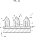
- FIG. 1A is a cross-sectional view illustrating a structure of a light-emitting device 10 according to an embodiment.
- the light-emitting device 10 may be, for example, a micro-light-emitting diode (micro-LED).
- the light-emitting device 10 may be a nanostructure light-emitting device.
- a core 3 may be referred to as a nano-core or nano-rod.
- the light-emitting device 10 may include a base semiconductor layer 2, at least one core 3 (hereinafter referred to as a single core for convenience of description), a first insulating layer 5a, and a light-emitting portion 4.
- the substrate 1 is a growth substrate for semiconductor single crystal growth, and a silicon (Si) substrate, a silicon carbide (SiC) substrate, a sapphire substrate, etc. may be used as the substrate 1.
- a material suitable for growth of the base semiconductor layer 2 to be formed on the substrate 1 for example, AlN, AlGaN, ZnO, GaAs, MgAl 2 O 4 , MgO, LiAlO 2 , LiGaO 2 , or GaN, may be used as the substrate 1.
- the substrate 1 may be removed after manufacturing of the light-emitting device 10 is completed through a manufacturing process to be described below.
- the base semiconductor layer 2 may be formed on the substrate 1.
- the base semiconductor layer 2 may function as a growth template for the core 3.
- the base semiconductor layer 2 may include the same material as the core 3.
- crystal defects due to lattice mismatch may be reduced when growing the core 3 on the base semiconductor layer 2.
- the base semiconductor layer 2 may include a Group III-V nitride semiconductor material.
- the base semiconductor layer 2 may be a first conductivity type semiconductor layer doped with a first type impurity.
- the base semiconductor layer 2 may include a GaN-based semiconductor material.
- the base semiconductor layer 2 may be a GaN layer doped with an n-type impurity (that is, an n-GaN layer).
- the base semiconductor layer 2 may have a multi-layered structure. Depending on a device to which the light-emitting device 10 is applied, the base semiconductor layer 2 may be removed after manufacturing of the light-emitting device 10 is completed through a manufacturing process to be described below.
- the core 3 is formed on the base semiconductor layer 2.
- the core 3 may include a body portion 31 and a shielding portion 32.
- the body portion 31 may extend from the base semiconductor layer 2 in a first direction D1 (for example, in a direction perpendicular to an upper surface 21 of the base semiconductor layer 2).
- a side surface 311 of the body portion 31 is a non-polar plane (that is, an m-plane).
- the shielding portion 32 is provided at an upper end of the body portion 31.
- the shielding portion 32 has a lower surface 321 having a width in a second direction D2 (that is perpendicular to the first direction D1) that is greater than a width of the body portion 31 in the second direction D2.
- the width of the shielding portion 32 in the second direction D2 may gradually decrease with the distance increasing from the lower surface 321 in the first direction D1. Accordingly, the upper surface 322 of the shielding portion 32 has a sharp shape inclined with respect to the lower surface 321.
- the upper surface 322 of the shielding portion 32 is a semipolar plane (that is, an r-plane).
- the core 3 may be formed on the base semiconductor layer 2 using the base semiconductor layer 2 as a template. As described above, the core 3 may include the same material as the base semiconductor layer 2.
- the core 3 may include a Group III-V nitride semiconductor material.
- the core 3 may include a first conductivity type semiconductor material doped with a first type impurity.
- the core 3 may include a GaN-based semiconductor material.
- the core 3 may include GaN doped with an n-type impurity (that is, n-GaN). Si, Ge, Se, Te, etc. may be used as the n-type impurity.
- the first insulating layer 5a at least partially covers the upper surface 21 of the base semiconductor layer 2 and the upper surface 322 of the shielding portion 32.
- the first insulating layer 5a may include a first portion 51 at least partially covering the upper surface 21 of the base semiconductor layer 2 and a second portion 52 at least partially covering the upper surface 322 of the shielding portion 32.
- the first insulating layer 5a may include an insulating material, such as silicon oxide or silicon nitride.
- the first insulating layer 5a may include, for example, SiO 2 , SiN, TiO 2 , Si 3 N 4 , Al 2 O 3 , TiN, AlN, ZrO 2 , TiAIN, or TiSiN.
- the shielding portion 32 of the core 3 in the second direction D2 functions as a mask to prevent an insulating material from being deposited on a side surface 311 of the body portion 31. Therefore, in the process of forming the first insulating layer 5a, no insulating material is deposited on the side surface 311 of the body portion 31.
- An insulating material may be deposited on the upper surface 21 of the base semiconductor layer 2 and the upper surface 322 of the shielding portion 32, excluding the side surface 311 of the body portion 31.
- the light-emitting portion 4 is formed on the side surface 311 of the body portion 31 of the core 3.
- the light-emitting portion 4 may include a Group III-V nitride semiconductor material.
- the light-emitting portion 4 may include a GaN-based semiconductor material.
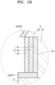
- FIG. 1B is an enlarged view of portion "A" in FIG. 1A illustrating a light-emitting portion 4 according to an embodiment.
- the light-emitting portion 4 may have a layered structure grown in the second direction D2 on the side surface 311 of the body portion 31 of the core 3.
- the light-emitting portion 4 may include a first conductivity type semiconductor layer 41 formed on the side surface 311 of the body portion 31 of the core 3, an active layer 42 having a quantum well structure at least partially covering the first conductivity type semiconductor layer 41, and a second conductivity type semiconductor layer 43 at least partially covering the active layer 42.
- the first conductivity type semiconductor layer 41 may be formed by being grown in the second direction D2 on the side surface 311 of the body portion 31 of the core 3.
- the first conductivity type semiconductor layer 41 may be a semiconductor layer doped with the first type impurity that is the same as those of the base semiconductor layer 2 and the core 3.
- the first conductivity type semiconductor layer 41 may be an n-GaN layer.
- the active layer 42 emits light through electron-hole recombination.
- the active layer 42 may be formed by being grown in the second direction D2 on the first conductivity type semiconductor layer 41.
- the active layer 42 has a quantum well structure.
- the active layer 42 may have a single quantum well or multi quantum well structure made by adjusting a band spacing by periodically changing x, y, and z values in Al x Ga y In z N.
- a quantum well layer and a barrier layer may be paired in the form of InGaN/GaN, InGaN/InGaN, InGaN/AlGaN, or InGaN/InAlGaN to form a quantum well structure, and the bandgap energy may be controlled according to a composition ratio of indium (In) in a material layer including indium (In), thereby adjusting a light emission wavelength band.
- the second conductivity type semiconductor layer 43 may at least partially cover the surface of the active layer 42.
- the second conductivity type semiconductor layer 43 may be formed by being grown in the second direction D2 on the active layer 42.
- the second conductivity type semiconductor layer 43 may be a semiconductor layer doped with a second type impurity.
- the second conductivity type semiconductor layer 43 may be a p-GaN layer doped with a p-type impurity. Mg, Zn, Be, etc. may be used as the p-type impurity.
- the light-emitting portion 4 may be formed by methods, such as hybrid vapor phase epitaxy (HVPE), molecular beam epitaxy (MBE), metal organic vapor phase epitaxy (MOVPE), and metal organic chemical vapor deposition (MOCVD).
- HVPE hybrid vapor phase epitaxy
- MBE molecular beam epitaxy
- MOVPE metal organic vapor phase epitaxy
- MOCVD metal organic chemical vapor deposition
- QCSE quantum confinement stark effect
- the light-emitting portion 4 is formed by being grown on the side surface 311 of the body portion 31 of the core 3.
- the side surface 311 of the body portion 31 of the core 3 is a non-polar plane (that is, an m-plane). Therefore, the problem of lowering internal quantum efficiency due to an internal magnetic field may be solved.
- polarization due to the piezoelectric field effect may be suppressed, and thus, the QCSE may be suppressed. Accordingly, internal quantum efficiency may be increased.
- the indium (In) content of the light-emitting portion 4 increases, the occurrence of crystal defects may be reduced.
- the light-emitting portion 4 that generates red light with high efficiency may be implemented. Because the light-emitting portion 4 is formed around the body portion 31 of the core 3, the light-emitting device 10 having the light-emitting portion 4 with an increased emission area compared to a planar light-emitting structure stacked in the first direction D1 may be implemented.
- the shielding portion 32 of the core 3 functions as a mask to prevent the first insulating layer 5a from being formed on the side surface 311 of the body portion 31, a process of forming a mask for selectively forming the first insulating layer 5a and a process of removing the mask after forming the first insulating layer 5a may be omitted. Accordingly, a process of manufacturing the light-emitting device 10 may be simplified and manufacturing costs may be reduced. In addition, the risk of damage and performance deterioration of the light-emitting device 10 due to the mask formation and removal process may be reduced, and thus, a reliable light-emitting device 10 may be manufactured.
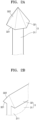
- FIGS. 2A and 2B are perspective views illustrating various shapes of a core 3 according to an embodiment.
- the body portion 31 of the core 3 may be pillar-shaped.
- the cross-sectional shape of the body portion 31 of the core 3 orthogonal to the first direction D1 may have various shapes, such as a circular shape, an oval shape, or a polygonal shape.
- the shape of the shielding portion 32 of the core 3 may be determined by the crystal lattice form of a material forming the core 3.
- the shielding portion 32 may have a hexahedral shape with a hexagonal bottom. As shown in FIG.
- the body portion 31 of the core 3 may have a stripe shape extending in the second direction D2.
- the shape of the core 3 is not limited to the shapes shown in FIGS. 2A and 2B .
- the core 3 may have various shapes including a shielding portion 32 having a width in the second direction D2 that is greater than a width of the body portion 31 in the second direction D2.
- FIG. 3 is a cross-sectional view illustrating a structure of a light-emitting device 10 according to an embodiment.
- the embodiment of the light-emitting device 10 shown in FIG. 3 is different from the embodiment of the light-emitting device 10 shown in FIGS. 1A , 1B , 2A, and 2B in that an insulating layer is partially formed on the side surface 311 of the body portion 31 of the core 3. Repeated description of aspects shown in FIGS. 1A , 1B , 2A, and 2B may be omitted.
- the light-emitting device 10 may include a second insulating layer 5b that at least partially covers the side surface 311 of the body portion 31 of the core 3.
- the second insulating layer 5b at least partially covers a portion (e.g., portion 390) of the side surface 311 of the body portion 31, the portion 390 being adjacent to the base semiconductor layer 2.
- an insulating layer 53 extends from the first insulating layer 5a (for example, the first portion 51) formed on the base semiconductor layer 2 along the side surface 311 of the body portion 31 in the first direction D1.
- the second insulating layer 5b may include, for example, SiO 2 , SiN, TiO 2 , Si 3 N 4 , Al 2 O 3 , TiN, AlN, ZrO 2 , TiAIN, or TiSiN.
- the second insulating layer 5b may be formed together with the first insulating layer 5a in the process of forming the first insulating layer 5a.
- the light-emitting portion 4 is formed on a portion of the side surface 311 of the body portion 31 in which the second insulating layer 5b is not formed.
- the light-emitting portion 4 may be formed on a portion of the side surface 311 of the body portion 31 that is between the second insulating layer 5b and the lower surface 321 of the shielding portion 32.
- an adjacent portion 390 i.e., a first portion
- a non-adjacent portion 392 i.e., a second portion
- the non-adjacent portion 392 may have the light-emitting portion 4 formed thereon
- the adjacent portion 390 may have the insulating layers 5a and 5b formed thereon.
- a portion of the side surface 311 of the body portion 31 that is adjacent to the base semiconductor layer 2 may refer to a portion close to the upper surface 21 of the base semiconductor layer 2 (which is a polar plane), and the quality of the adjacent portion as a non-polar plane may be relatively low compared to that of a portion further away from the base semiconductor layer 2 in the first direction D1.
- the half-width of an emission wavelength may increase due to a difference in material composition of the light-emitting portion 4 in the first direction D1, thereby deteriorating the emission quality.
- the light-emitting portion 4 is not grown in the adjacent portion of the side surface 311 of the body portion 31.
- the light-emitting portion 4 is formed on a portion (e.g., portion 392) of the side surface 311 of the body portion 31, which is above the adjacent portion in the first direction D1. That is, because the light-emitting portion 4 is grown on a non-polar plane of relatively good quality, the material composition of the light-emitting portion 4 may be uniform in the first direction D1. As a result, an increase in the half width of the emission wavelength due to a difference in the material composition of the light-emitting portion 4 may be prevented.
- FIG. 4 is a cross-sectional view illustrating a structure of a light-emitting device 10 according to an embodiment.
- the embodiment of the light-emitting device 10 shown in FIG. 4 is different from the embodiment of the light-emitting device 10 shown in FIGS. 1 to 3 in that the light-emitting device 10 shown in FIG. 4 includes a plurality of cores with body portions 31 of different widths in the second direction D2. Repeated description of aspects shown in FIGS. 1A , 1B , 2A, 2B , and 3 may be omitted.
- the 'width of the core in the second direction D2' may refer to the diameter of an equivalent circle corresponding to the cross-section of a body portion when the body portion has a column shape with a cross-section of, for example, a circular, oval, or polygonal shape, or may refer to the minimum diameter of a circle including the cross-section of the body portion.
- the 'width of the core in the second direction D2' may refer to the width of the body portion in a short axis direction.
- the cores 3-1, 3-2, and 3-3 include body portions 31-1, 31-2, and 31-3 and shielding portions 32-1, 32-2, and 32-3, respectively.
- the widths of the body portions 31-1, 31-2, and 31-3 in the second direction D2 are S11, S21, and S31, respectively. In some embodiments, S11 ⁇ S21 ⁇ S31.
- the heights of the body portions 31-1, 31-2, and 31-3 in the first direction D1 are the same, but at least one of the body portions 31-1, 31-2, and 31-3 may have a different height from the rest.
- the description of the body portion 31 given above applies to the body portions 31-1, 31-2, and 31-3.
- each of the shielding portions 32-1, 32-2, and 32-3 in the second direction D2 may be greater than the widths of the body portions 31-1, 31-2, and 31-3 in the second direction D2.
- the description of the shielding portion 32 given above applies to the shielding portions 32-1, 32-2, and 32-3.
- the first insulating layer 5a may include a first portion 51 formed on the upper surface 21 of the base semiconductor layer 2 and second portions 52 respectively formed on the upper surfaces of the shielding portions 32-1, 32-2, and 32-3.
- Second insulating layers 5b-1, 5b-2, and 5b-3 at least partially cover the side surfaces 311-1, 311-2, and 311-3 of the body portions 31-1, 31-2, and 31-3, respectively.
- the description of the second insulating layer 5b given above applies to the second insulating layer 5b-1, 5b-2, and 5b-3.
- the heights of the second insulating layers 5b-1, 5b-2, and 5b-3 in the first direction D1 may be different from each other. For example, when the heights of the second insulating layers 5b-1, 5b-2, and 5b-3 in the first direction D1 are H11, H21, and H31, respectively, H11 ⁇ H21 ⁇ H31.
- Light-emitting portions 4-1, 4-2, and 4-3 are respectively formed on portions of the side surfaces of the body portions 31-1, 31-2, and 31-3, which are not covered by the second insulating layers 5b-1, 5b-2, and 5b-3.
- the description of the light-emitting portion 4 given above applies to the light-emitting portions 4-1, 4-2, and 4-3.
- the indium (In) contents of the light-emitting portions 4-1, 4-2, and 4-3 may be different from each other.
- the heights of the light-emitting portions 4-1, 4-2, and 4-3 in the first direction D1 may be different from each other.
- the heights of the body portions 31-1, 31-2, and 31-3 in the first direction D1 may be the same, and the heights of the second insulating layers 5b-1, 5b-2, and 5b-3, in the first direction D1, respectively formed on the side surfaces 311-1, 311-2, and 311-3 of the body portions 31-1, 31-2, and 31-3 may be different from each other.
- the heights of the light-emitting portions 4-1, 4-2, and 4-3 in the first direction D1 are respectively H12, H22, and H32, H12>H22>H32.
- the widths of the light-emitting portions 4-1, 4-2, and 4-3 in the second direction D2 may be different from each other.
- the widths of the light-emitting portions 4-1, 4-2, and 4-3 in the second direction D2 are respectively S12, S22, and S32, S12 ⁇ S22 ⁇ S32.
- the light-emitting portions 4-1, 4-2, and 4-3 may emit light having different colors (that is, different wavelengths).
- the emission wavelength depends on the content of indium (In). The higher the indium (In) content, the longer the emission wavelength.
- the total amounts of indium (In) supplied per unit time to the cores 3-1, 3-2, and 3-3 are the same. Therefore, the smaller the sizes of the light-emitting portions 4-1, 4-2, and 4-3, the higher the indium (In) content.
- the light-emitting portion 4-1 with the smallest width S12 has the highest content of indium (In)
- the light-emitting portion 4-3 with the largest width S32 has the lowest content of indium (In). Therefore, in terms of the emission wavelength, the emission wavelength becomes shorter in the order of the light-emitting portion 4-1, the light-emitting portion 4-2, and the light-emitting portion 4-3.
- the widths of the light-emitting portions 4-1, 4-2, and 4-3 in the second direction D2 may be adjusted such that the light-emitting portions 4-1, 4-2, and 4-3 emit red light R, green light G, and blue light B, respectively.
- the widths S12, S22, and S32 of the light-emitting portions 4-1, 4-2, and 4-3 in the second direction D2 may be adjusted by the heights H12, H22, and H32 of the light-emitting portions 4-1, 4-2, and 4-3 in the first direction D1.
- the heights H12, H22, and H32 of the light-emitting portions 4-1, 4-2, and 4-3 in the first direction D1 may be adjusted by the heights H11, H21, and H31 of the second insulating layers 5b-1, 5b-2, and 5b-3 in the first direction D1.
- the light-emitting portions 4-1, 4-2, and 4-3 are grown on the non-polar plane, thereby suppressing the QCSE, and thus, a monolithic color light-emitting device capable of emitting three-color light with stable wavelength characteristics may be implemented.
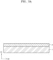
- FIGS. 5A to 5G are diagrams illustrating a method of manufacturing a light-emitting device 10 according to an embodiment.
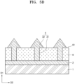
- the method of manufacturing the light-emitting device 10 according to an embodiment may include forming a base semiconductor layer 2 on a substrate 1 (see FIG. 5A ), forming a mask layer 6 defining a growth hole 6a on the base semiconductor layer 2 (see FIG. 5B ), forming a core 3 having a body portion 31 filling the growth hole 6a and a shielding portion 32 larger than the body portion 31 (see FIGS. 5C and 5D ), removing the mask layer 6 (see FIG. 5E ), forming a first insulating layer 5a (see FIG. 5F ), and forming a light-emitting portion 4 on a side surface 311 of the body portion 31 (see FIG. 5G ).
- each operation will be described in detail.
- the base semiconductor layer 2 is formed on the substrate 1.
- the substrate 1 is a growth substrate for semiconductor single crystal growth, and a silicon (Si) substrate, a silicon carbide (SiC) substrate, a sapphire substrate, etc. may be used as the substrate 1.
- a substrate including a material suitable for the growth of the base semiconductor layer 2 to be formed on the substrate 1 may be used (for example, AlN, AlGaN, ZnO, GaAs, MgAl 2 O 4 , MgO, LiAlO 2 , LiGaO 2 , or GaN).
- the base semiconductor layer 2 may include a Group III-V nitride semiconductor material (for example, a GaN-based semiconductor material).
- the base semiconductor layer 2 may be a first conductivity type semiconductor layer.
- the base semiconductor layer 2 may be formed by various methods, such as HVPE, MBE, MOVPE, and MOCVD.
- GaN may be grown on the substrate 1 and doped with an n-type impurity, such as Si, Ge, Se, or Te, to form an n-GaN layer.
- a buffer layer for epitaxial growth may be further formed between the substrate 1 and the base semiconductor layer 2.
- a mask layer 6 defining at least one growth hole 6a is formed on the base semiconductor layer 2.
- the mask layer 6 may be etched by a lithography method (for example, a photo lithography method or an electron beam lithography method), and thus, at least one growth hole 6a may be formed in the mask layer 6.
- the growth hole 6a may have various shapes, such as circular, oval, polygonal, and striped shapes.
- the upper surface 21 of the base semiconductor layer 2 is partially exposed through the growth hole 6a.
- the mask layer 6 may include SiO 2 , TiO 2 , Si 3 N 4 , Al 2 O 3 , TiN, AlN, ZrO 2 , TiAlN, TiSiN, etc.
- the SiO 2 layer may be etched to form the growth hole 6a exposing the upper surface 21 of the base semiconductor layer 2.
- the height of the mask layer 6 in the first direction D1 may correspond to the height of the body portion 31 of the core 3, to be formed later, in the first direction D1.
- the core 3 may include a Group III-V nitride semiconductor material (for example, a GaN-based semiconductor material).
- the core 3 may be a first conductivity type semiconductor layer.
- the core 3 may be formed by various methods, such as HVPE, MBE, MOVPE, and MOCVD.
- GaN may be grown from the upper surface 21 of the base semiconductor layer 2 through the growth hole 6a.
- GaN grows from the upper surface 21 of the base semiconductor layer 2 in the first direction D1 to at least partially fill the inside of the growth hole 6a. When GaN fills the entire inside of the growth hole 6a, as shown in FIG.
- the body portion 31 extending from the upper surface 21 of the base semiconductor layer 2 in the first direction D1 is formed.
- GaN gradually grows from an upper end of the body portion 31 in the first direction D1, as shown by the dotted line in FIG. 5D , and also grows in the second direction D2 orthogonal to the first direction D1 along an upper surface 61 of the mask layer 6.
- the lower surface 321 of the shielding portion 32 extends in the second direction D2 along the upper surface 61 of the mask layer 6. Accordingly, the width of the lower surface 321 of the shielding portion 32 in the second direction D2 may be greater than that of the body portion 31.
- the shape of the shielding portion 32 may be determined by the crystal lattice structure of a material forming the core 3.
- the shielding portion 32 having a width in the second direction D2 that is greater than a width of the body portion 31 in the second direction D2 is formed on the upper surface 61 of the mask layer 6.
- the shielding portion 32 may have a seven-sided shape with a hexagonal bottom.
- the mask layer 6 is removed (for example, by a wet etching process).
- the core 3 which includes the body portion 31 extending from the upper surface 21 of the base semiconductor layer 2 in the first direction D1 and the shielding portion 32 having a width in the second direction D2 that is greater than a width of the body portion 31 in the second direction D2, may be formed.
- the shielding portion 32 has a lower surface 321 having a width in the second direction D2 that is greater than a width of the body portion 31 in the second direction D2, and an upper surface 322 that extends obliquely from the lower surface 321 in the first direction D1 and is sharp overall.
- the core 3 may include the same material as the base semiconductor layer 2 (for example, a first conductivity type semiconductor material).
- the base semiconductor layer 2 is a GaN-based first conductivity type semiconductor layer (that is, an n-GaN layer).
- the core 3 including GaN may be doped with an n-type impurity, such as Si, Ge, Se, or Te. Accordingly, the core 3 may include the same n-GaN as the base semiconductor layer 2.
- the first insulating layer 5a is formed to at least partially cover a polar plane and a semipolar plane.
- the first insulating layer 5a may not be formed on a non-polar plane.
- the first insulating layer 5a may include an insulating material (for example, SiO 2 , TiO 2 , Si 3 N 4 , Al 2 O 3 , TiN, AlN, ZrO 2 , TiAlN, or TiSiN).
- the first insulating layer 5a includes SiO 2 .
- the first insulating layer 5a may be formed by plasma deposition.
- the upper surface 21 of the base semiconductor layer 2 is a polar plane.
- the upper surface 322 of the shielding portion 32 is a semipolar plane.
- the side surface 311 of the body portion 31 is a non-polar plane. Because the upper surface 21 of the base semiconductor layer 2 and the upper surface 322 of the shielding portion 32 are not covered by the shielding portion 32, as shown in FIG. 5F , an insulating material is deposited on the upper surface 21 of the base semiconductor layer 2 and the upper surface 322 of the shielding portion 32 to form a first insulating layer 5a (for example, a first portion 51 and a second portion 52).
- the light-emitting portion 4 may include a Group III-V nitride semiconductor material (for example, a GaN-based semiconductor material).
- the light-emitting portion 4 may be formed by sequentially growing a first conductivity type semiconductor layer 41, an active layer 42, and a second conductivity type semiconductor layer 43 on the side surface 311 of the body portion 31 by using various methods, such as HVPE, MBE, MOVPE, and MOCVD.
- An n-GaN layer is grown as the first conductivity type semiconductor layer 41 on the side surface 311 of the body portion 31.
- the first conductivity type semiconductor layer 41 grows from the side surface 311 of the body portion 31 in the second direction D2. Because the upper surface 21 of the base semiconductor layer 2 and the upper surface 322 of the shielding portion 32 are at least partially covered by the first insulating layer 5a, the n-GaN layer is not grown thereon.
- the active layer 42 is grown on the first conductivity type semiconductor layer 41.
- the active layer 42 may have a single quantum well or multi quantum well structure.
- a quantum well layer and a barrier layer may be paired in the form of InGaN/GaN, InGaN/InGaN, InGaN/AlGaN, or InGaN/InAlGaN to form a quantum well structure.
- the active layer 42 grows from the first conductivity type semiconductor layer 41 in the second direction D2.
- the second conductivity type semiconductor layer 43 at least partially covering the active layer 42 is grown.
- the second conductivity type semiconductor layer 43 is grown from the active layer 42 in the second direction D2.
- the second conductivity type semiconductor layer 43 is a p-GaN layer.
- the light-emitting device 10 may be manufactured through the process shown in FIGS. 5A to 5G described above.
- a process of forming electrodes for supplying current to the first conductivity type semiconductor layer 41 and the second conductivity type semiconductor layer 43 may be further performed.
- a method of forming on the base semiconductor layer 2 an n-GaN layer having uniform thickness and etching the n-GaN layer to form the core may be considered.
- the core formed by etching that is, the side surface of a body portion
- an annealing process may be added after etching.
- a separate process may be required to form a shielding portion after forming the body portion.
- GaN is grown inside the growth hole 6a defined by the mask layer 6.
- the core 3 having the body portion 31 may be formed, and it is easy to control the shape of the body portion 31 of the core 3.
- a core 3 with a high aspect ratio may be formed.
- the shielding portion 32 is naturally formed. In other words, the body portion 31 and the shielding portion 32 are formed through the same process. Therefore, the manufacturing process may be simplified.
- the light-emitting portion may be prevented from growing on a polar plane and a semipolar plane.
- a method of forming a mask for protecting the non-polar plane when forming a first insulating layer at least partially covering the polar plane and the semipolar plane and removing the mask after forming the first insulating layer at least partially covering the polar plane and the semipolar plane may be considered.
- the process of forming/removing the mask involves an etching process, which may damage the core.
- additional processes such as etching a grown light-emitting portion or forming a high-resistance layer on the light-emitting portion, may be added such that the light-emitting portion grown on the semipolar plane does not emit light. This additional process may cause damage or deterioration of performance of the manufactured light-emitting device.
- the shielding portion 32 of the core 3 functions as a mask that protects the side surface 311 of the body portion 31 (which is a non-polar plane). Therefore, the process of forming/removing a mask to protect the non-polar plane may be omitted, and thus, the manufacturing process may be simplified, the manufacturing cost may be reduced, and the risk of damage to the core 3 in the manufacturing process may be reduced.
- the body portion 31 includes the same material as the first conductivity type semiconductor layer 41 (for example, n-GaN). Accordingly, the lattice mismatch between the body portion 31 and the first conductivity type semiconductor layer 41 may be minimized, and thus, a first conductivity type semiconductor layer 41 grown with good quality and an active layer 42 grown on the first conductivity type semiconductor layer 41 may be obtained.
- the side surface 311 of the body portion 31 is a non-polar plane. Accordingly, the problem of lowering internal quantum efficiency due to an internal magnetic field may be solved, and polarization due to the piezoelectric field effect may be suppressed, thereby suppressing the QCSE. Accordingly, the light-emitting portion 4 with increased internal quantum efficiency may be implemented.
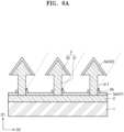
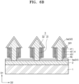
- FIGS. 6A and 6B are diagrams illustrating a method of manufacturing a light-emitting device 10 according to an embodiment.
- differences from the embodiment of the manufacturing method shown in FIGS. 5A to 5G will be mainly described, and repeated descriptions will be omitted.
- the core 3 which includes the body portion 31 extending from the upper surface 21 of the base semiconductor layer 2 in the first direction D1 and the shielding portion 32 having a width in the second direction D2 that is greater than a width of the body portion 31 in the second direction D2, is formed.
- the first and second insulating layers 5a and 5b may include an insulating material (for example, SiO 2 , TiO 2 , Si 3 N 4 , Al 2 O 3 , TiN, AlN, ZrO 2 , TiAlN, or TiSiN).
- the first and second insulating layers 5a and 5b include SiO 2 .
- the first and second insulating layers 5a and 5b may be formed by plasma deposition.
- the first insulating layer 5a is formed on the upper surface 21 of the base semiconductor layer 2 (which is a polar plane), and the upper surface 322 of the shielding portion 32 (which is a semipolar plane), and the second insulating layer 5b is formed to at least partially cover a portion of the side surface 311 of the body portion 31 (which is a non-polar plane) that is adjacent to the base semiconductor layer 2. Because the upper surface 21 of the base semiconductor layer 2 and the upper surface 322 of the shielding portion 32 are not covered by the shielding portion 32, an insulating material is deposited on the upper surface 21 of the base semiconductor layer 2 and the upper surface 322 of the shielding portion 32 to form a first insulating layer 5a including a first portion 51 and a second portion 52.
- the side surface 311 of the body portion 31 is at least partially covered by the shielding portion 32.
- process conditions such as process temperature and process pressure, may be adjusted such that an insulating material is not deposited on a portion of the side surface 311 of the body portion 31 that is above the adjacent portion (e.g., portion 392 that is above portion 390 of FIG. 3 ) due to the shadow effect of the shielding portion 32 and, as indicated by an arrow in FIG. 6A , an insulating material is deposited on the portion of the side surface 311 of the body portion 31 that is adjacent to the base semiconductor layer 2.
- the first insulating layer 5a may be formed on the upper surface 21 of the base semiconductor layer 2 and the upper surface 322 of the shielding portion 32, and the second insulating layer 5b may be formed on the portion of the side surface 311 of the body portion 31 that is adjacent to the base semiconductor layer 2.
- a process of forming the light-emitting portion 4 is performed as shown in FIG. 6B .
- the process of forming the light-emitting portion 4 is the same as described in FIG. 5G .
- the light-emitting portion 4 is formed on a portion of the side surface 311 of the body portion 31 that is above the portion adjacent to the base semiconductor layer 2 and on which the second insulating layer 5b is not formed (that is, the light-emitting portion 4 is formed on a portion between the second insulating layer 5b and the lower surface 321 of the shielding portion 32).
- the light-emitting device 10 according to an embodiment shown in FIG. 3 may be manufactured.
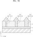
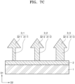
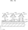
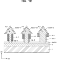
- FIGS. 7A to 7E are diagrams illustrating a method of manufacturing a light-emitting device 10 according to an embodiment.
- differences from the embodiment of the manufacturing method shown in FIGS. 5A to 5G will be mainly described, and repeated descriptions will be omitted.
- the base semiconductor layer 2 may include a Group III-V nitride semiconductor material (for example, a GaN-based semiconductor material).
- the base semiconductor layer 2 may be a first conductivity semiconductor layer (for example, an n-GaN layer).
- GaN may be grown on the substrate 1 and doped with an n-type impurity, such as Si, Ge, Se, or Te, to form the base semiconductor layer 2 (which is an n-GaN layer).
- a mask layer defining growth holes having different widths in the second direction D2 on the base semiconductor layer 2 (for example, growth holes 6a1, 6a2, and 6a3) is formed.
- the widths of the growth holes 6a1, 6a2, and 6a3 in the second direction D2 are S11, S21, and S31, respectively, and may be S11 ⁇ S21 ⁇ S31.
- the mask layer 6 may be etched by a lithography method (for example, a photo lithography method or an electron beam lithography method), and thus, the growth holes 6a1, 6a2, and 6a3 may be formed in the mask layer 6.
- the growth holes 6a1, 6a2, and 6a3 may have various shapes, such as circular, oval, polygonal, and striped shapes.
- the upper surface 21 of the base semiconductor layer 2 is exposed by the growth holes 6a1, 6a2, and 6a3.
- the mask layer 6 may include SiO 2 , TiO 2 , Si 3 N 4 , Al 2 O 3 , TiN, AlN, ZrO 2 , TiAlN, TiSiN, etc.
- the SiO 2 layer may be etched to form the growth holes 6a1, 6a2, and 6a3 exposing the upper surface 21 of the base semiconductor layer 2.
- the height of the mask layer 6 in the first direction D1 may correspond to the height of the body portion 31 of the core 3, to be formed later, in the first direction D1.
- forming cores 3-1, 3-2, and 3-3 grown from the upper surface 21 of the base semiconductor layer 2 through the growth holes 6a1, 6a2 and 6a3 is performed.
- the forming of the cores 3-1, 3-2, and 3-3 may be performed with the same as the process shown in FIGS. 5D and 5E described above.
- GaN may be grown from the upper surface 21 of the base semiconductor layer 2 through the growth holes 6a1, 6a2, and 6a3.
- GaN grows from the upper surface 21 of the base semiconductor layer 2 in the first direction D1 to fill the insides of the growth holes 6a1, 6a2, and 6a3, body portions 31-1, 31-2, and 31-3 extending from the upper surface 21 of the base semiconductor layer 2 in the first direction D1 are formed.
- GaN gradually grows from upper ends of the body portions 31-1, 31-2, and 31-3 in the first direction D1, as shown by the dotted line in FIG. 5D , and also grows in the second direction D2 orthogonal to the first direction D1 along the upper surface 61 of the mask layer 6.
- the shape of the shielding portion 32 may be determined by the crystal lattice structure of a material forming the core 3. Shielding portions 32-1, 32-2, and 32-3 having widths in the second direction D2 that are greater than the widths of the body portions 31-1, 31-2, and 31-3 in the second direction D2 are formed on the upper surface 61 of the mask layer 6.
- the mask layer 6 is removed (for example, by a wet etching process).
- the cores 3-1, 3-2, and 3-3 which respectively include the body portions 31-1, 31-2, and 31-3 extending from the upper surface 21 of the base semiconductor layer 2 in the first direction D1 and the shielding portions 32-1, 32-2, and 32-3 having widths in the second direction D2 that are greater than the widths of the body portions 31-1, 31-2, and 31-3 in the second direction D2, may be formed.
- the cores 3-1, 3-2, and 3-3 may include the same material as the base semiconductor layer 2 (for example, a first conductivity type semiconductor material).
- the base semiconductor layer 2 is a GaN-based first conductivity type semiconductor layer (for example, an n-GaN layer).
- the cores 3-1, 3-2, and 3-3 including GaN may be doped with an n-type impurity, such as Si, Ge, Se, or Te. Accordingly, the cores 3-1, 3-2, and 3-3 may include the same n-GaN as the base semiconductor layer 2.
- the first and second insulating layers 5a and 5b may include an insulating material (for example, SiO 2 , TiO 2 , Si 3 N 4 , Al 2 O 3 , TiN, AlN, ZrO 2 , TiAlN, or TiSiN).
- the first and second insulating layers 5a and 5b include SiO 2 .
- the first and second insulating layers 5a and 5b may be formed by plasma deposition.
- the first insulating layer 5a is formed on the upper surface 21 of the base semiconductor layer 2 (which is a polar plane), and the upper surfaces 322-1, 322-2, and 322-3 of the shielding portions 32-1, 32-2, and 32-3 (which are semipolar planes).
- the second insulating layer 5b is formed to at least partially cover portions which are adjacent to the base semiconductor layer 2, of the side surfaces 311-1, 311-2, and 311-3 of the body portions 31-1, 31-2, and 31-3 (which are non-polar planes).
- an insulating material is deposited on the upper surface 21 of the base semiconductor layer 2 and the upper surfaces 322-1 , 322-2, and 322-3 of the shielding portions 32-1, 32-2, and 32-3 to form a first portion 51 and second portions 52-1, 52-2, and 52-3.
- the side surfaces 311-1, 311-2, and 311-3 of the body portions 31-1, 31-2, and 31-3 are at least partially covered by the shielding portions 32-1, 32-2, and 32-3.
- an insulating material is deposited on portions of the side surfaces 311-1, 311-2, and 311-3 of the body portions 31-1, 31-2, and 31-3 that are adjacent to the upper surface 21 of the base semiconductor layer 2.
- second insulating layers 5b-1, 5b-2, and 5b-3 may be formed on the side surfaces 311-1, 311-2, and 311-3 of the body portion 31-1, 31-2, and 31-3.
- Process conditions such as process temperature and process pressure, may be determined such that an insulating material may be partially deposited onto portions of the side surfaces 311-1, 311-2, and 311-3 of the body portions 31-1, 31-2, and 31-3 that are adjacent to the upper surface 21 of the base semiconductor layer 2.
- the widths of the shielding portions 32-1, 32-2, and 32-3 in the second direction D2 are approximately the same.
- the widths of the body portions 31-1, 31-2, and 31-3 in the second direction D2 are different from each other and have a relationship of S11 ⁇ S21 ⁇ S31, and thus, the extent to which the shading effect of the shielding portions 32-1, 32-2, and 32-3 affects each of the body portions 31-1, 31-2, and 31-3 varies. Accordingly, the heights of the second insulating layers 5b-1, 5b-2, and 5b-3 respectively formed on the side surfaces 311-1, 311-2, and 311-3 of the body portions 31-1, 31-2, and 31-3 vary. When the heights of the second insulating layers 5b-1, 5b-2, and 5b-3 in the first direction D1 are respectively H11, H21, and H31, H11 ⁇ H21 ⁇ H31.
- forming light-emitting portions 4-1, 4-2, and 4-3 on the side surfaces 311-1, 311-2, and 311-3 of the body portions 31-1, 31-2, and 31-3, which are non-polar planes, is performed.
- the process of forming the light-emitting portions 4-1, 4-2, and 4-3 may be the same as the process described with reference to FIG. 5G .
- the structure of each of the light-emitting portions 4-1, 4-2, and 4-3 may be the same as that of the light-emitting portion 4.
- the light-emitting portions 4-1, 4-2, and 4-3 are formed on portions of the side surfaces 311-1, 311-2, and 311-3 of the body portions 31-1, 31-2, and 31-3 which are not covered by the second insulating layer 5b-1, 5b-2, and 5b-3. Accordingly, the light-emitting portions 4-1, 4-2, and 4-3 may be formed with different heights in the first direction D1 and different widths in the second direction D2.
- the light-emitting device 10 may be manufactured.
- the electronic devices may be displays or may be various devices including displays.
- FIG. 8 is a diagram illustrating a display according to an embodiment.
- the display may include a display panel 7110 and a controller 7160.
- the display panel 7110 has a light-emitting structure 7112 and a driving circuit 7115 that switches the light-emitting structure 7112 on and off.
- the light-emitting structure 7112 may include a plurality of light-emitting devices 10 described with reference to FIGS. 1 to 7E .
- the plurality of light-emitting devices 10 may be arranged, for example, in a two-dimensional array.
- the driving circuit 7115 has a plurality of switching elements for individually switching on-off the plurality of light-emitting devices 10.
- the controller 7160 inputs on-off switching signals of the plurality of light-emitting devices 10 to the driving circuit 7115 according to an image signal.
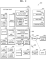
- FIG. 9 is a block diagram illustrating an electronic device including a display according to an embodiment.
- the electronic device 8201 may be provided in a network environment 8200.
- the electronic device 8201 may communicate with another electronic device 8202 through a first network 8298 (a short-range wireless communication network, etc.) or with another electronic device 8204 and/or a server 8208 through a second network 8299 (a remote wireless communication network, etc.).
- the electronic device 8201 may communicate with the electronic device 8204 through the server 8208.
- the electronic device 8201 may include a processor 8220, a memory 8230, an input device 8250, a sound output device 8255, a display apparatus 8260, an audio module 8270, a sensor module 8276, an interface 8277, a haptic module 8279, a camera module 8280, a power management module 8288, a battery 8289, a communication module 8290, a subscriber identification module 8296, and/or an antenna module 8297.
- the electronic device 8201 may omit some of these components or may further include other components. Some of these components may be implemented as an integrated circuit.
- the sensor module 8276 (a fingerprint sensor, an iris sensor, an illuminance sensor, etc.) may be embedded in the display apparatus 8260 (a display, etc.)
- the processor 8220 may execute software (a program 8240, etc.) to control one or more components (hardware, software, etc.) of the electronic device 8201 connected to the processor 8220 and to perform various data processing or computation operations. As part of the data processing or computation operations, the processor 8220 may be configured to load a command and/or data received from other components (the sensor module 8276, the communication module 8290, etc.) into a volatile memory 8232, process the command and/or the data stored in the volatile memory 8232, and store resulting data in a non-volatile memory 8234.
- software a program 8240, etc.
- the processor 8220 may include a main processor 8221 (a central processing unit, an application processor, etc.) and an auxiliary processor 8223 (a graphics processing unit, an image signal processor, a sensor-hub processor, a communication processor, etc.) which may operate separately from or together with the main processor 8221.
- the auxiliary processor 8223 may use less power than the main processor 8221 and may perform specialized functions.
- the auxiliary processor 8223 may operate instead of the main processor 8221, when the main processor 8221 is in an inactive state (a sleep state), may operate together with the main processor 8221, when the main processor 8221 is in an active state (an application execution state), and may control a function and/or a state associated with one or more components (the display apparatus 8260, the sensor module 8276, the communication module 8290, etc.) of the electronic device 8201.
- the auxiliary processor 8223 (the image signal processor, the communication processor, etc.) may be implemented as part of other functionally related components (the camera module 8280, the communication module 8290, etc.).
- the memory 8230 may store various data required by the components (the processor 8220, the sensor module 8276, etc.) of the electronic device 8201.
- the data may include, for example, the software (the program 8240, etc.), and input data and/or output data with respect to a command related to the software.
- the memory 8230 may include the volatile memory 8232 and/or the non-volatile memory 8234.
- the program 8240 may be stored in the memory 8230 as software and may include an operating system 8242, middleware 8244, and/or an application 8246.
- the input device 8250 may receive a command and/or data to be used for the components (the processor 8220, etc.) of the electronic device 8201, from the outside (a user, etc.) of the electronic device 8201.
- the input device 8250 may include a remote controller, a microphone, a mouse, a keyboard, and/or a digital pen (a stylus pen, etc.).
- the sound output device 8255 may output a sound signal to the outside of the electronic device 8201.
- the sound output device 8255 may include a speaker and/or a receiver.
- the speaker may be used for a general purpose, such as reproducing multimedia content or recording content, and the receiver may be used to receive an incoming call.
- the receiver may be integrated as part of the speaker or separately provided from the speaker.
- the display apparatus 8260 may visually provide data to the outside of the electronic device 8201.
- the display apparatus 8260 may include a display, a hologram device, or a control circuit configured to control a projector and a corresponding device.
- the display apparatus 8260 may include the display described with reference to FIG. 8 .
- the display apparatus 8260 may include the light-emitting device 10 described with reference to FIGS. 1 to 7E .
- the display apparatus 8260 may include touch circuitry configured to sense a touch operation and/or sensor circuitry (a pressure sensor, etc.) configured to measure an intensity of a force generated by the touch operation.
- the audio module 8270 may convert sound into an electrical signal or an electrical signal into sound.
- the audio module 8270 may obtain sound via the input device 8250 or may output sound via the sound output device 8255 and/or a speaker and/or a headphone of another electronic device (the electronic device 8202, etc.) directly or wirelessly connected to the electronic device 8201.
- the sensor module 8276 may sense an operation state (power, temperature, etc.) of the electronic device 8201 or an external environmental state (a user state, etc.) and generate electrical signals and/or data values corresponding to the sensed state.
- the sensor module 8276 may include a gesture sensor, a gyro-sensor, an atmospheric sensor, a magnetic sensor, an acceleration sensor, a grip sensor, a proximity sensor, a color sensor, an infrared (IR) sensor, a biometric sensor, a temperature sensor, a humidity sensor, and/or an illuminance sensor.
- the interface 8277 may support one or more designated protocols to be used for the electronic device 8201 to be directly or wirelessly connected to another electronic device (the electronic device 8202, etc.).
- the interface 8277 may include a high-definition multimedia interface (HDMI) interface, a universal serial bus (USB) interface, a secure digital (SD) card interface, and/or an audio interface.
- HDMI high-definition multimedia interface
- USB universal serial bus
- SD secure digital
- a connection terminal 8278 may include a connector, through which the electronic device 8201 may be physically connected to another electronic device (the electronic device 8202, etc.).
- the connection terminal 8278 may include an HDMI connector, a USB connector, an SD card connector, and/or an audio connector (a headphone connector, etc.).
- the haptic module 8279 may convert an electrical signal into a mechanical stimulus (vibration, motion, etc.) or an electrical stimulus which is recognizable to a user via haptic or motion sensation.
- the haptic module 8279 may include a motor, a piezoelectric device, and/or an electrical stimulus device.
- the camera module 8280 may capture a still image and a video.
- the camera module 8280 may include a lens assembly including one or more lenses, image sensors, image signal processors, and/or flashes.
- the lens assemblies included in the camera module 8280 may collect light emitted from an object, an image of which is to be captured.
- the power management module 8288 may manage power supplied to the electronic device 8201.
- the power management module 8288 may be realized as part of a power management integrated circuit (PMIC).
- PMIC power management integrated circuit
- the battery 8289 may supply power to the components of the electronic device 8201.
- the battery 8289 may include a non-rechargeable primary battery, rechargeable secondary battery, and/or a fuel battery.
- the communication module 8290 may support establishment of direct (wired) communication channels and/or wireless communication channels between the electronic device 8201 and other electronic devices (the electronic device 8202, the electronic device 8204, the server 8208, etc.) and communication performance through the established communication channels.
- the communication module 8290 may include one or more communication processors separately operating from the processor 8220 (an application processor, etc.) and supporting direct communication and/or wireless communication.
- the communication module 8290 may include a wireless communication module 8292 (a cellular communication module, a short-range wireless communication module, a global navigation satellite system (GNSS) communication module, and/or a wired communication module 8294 (a local area network (LAN) communication module, a power line communication module, etc.).
- GNSS global navigation satellite system
- wired communication module 8294 a local area network (LAN) communication module, a power line communication module, etc.
- a corresponding communication module may communicate with other electronic devices through the first network 8298 (a short-range wireless communication network, such as Bluetooth, WiFi direct, or infrared data association (IrDA)) or the second network 8299 (a remote communication network, such as a cellular network, the Internet, or a computer network (LAN, WAN, etc.)).
- a short-range wireless communication network such as Bluetooth, WiFi direct, or infrared data association (IrDA)
- the second network 8299 a remote communication network, such as a cellular network, the Internet, or a computer network (LAN, WAN, etc.)
- Various types of communication modules described above may be integrated as a single component (a single chip, etc.) or realized as a plurality of components (a plurality of chips).
- the wireless communication module 8292 may identify and authenticate the electronic device 8201 within the first network 8298 and/or the second network 8299 by using subscriber information (international mobile subscriber identification (IMSI), etc.) stored in the
- the antenna module 8297 may transmit a signal and/or power to the outside (other electronic devices, etc.) or receive the same from the outside.
- the antenna may include an emitter including a conductive pattern formed on a substrate (a printed circuit board (PCB), etc.).
- the antenna module 8297 may include an antenna or a plurality of antennas. When the antenna module 8297 includes a plurality of antennas, an appropriate antenna which is suitable for a communication method used in the communication networks, such as the first network 8298 and/or the second network 8299, may be selected. Through the selected antenna, signals and/or power may be transmitted or received between the communication module 8290 and other electronic devices.
- another component a radio frequency integrated circuit (RFIC), etc.
- RFIC radio frequency integrated circuit
- Some of the components of the electronic device 8201 may be connected to one another and exchange signals (commands, data, etc.) with one another, through communication methods performed among peripheral devices (a bus, general purpose input and output (GPIO), a serial peripheral interface (SPI), a mobile industry processor interface (MIPI), etc.).
- peripheral devices a bus, general purpose input and output (GPIO), a serial peripheral interface (SPI), a mobile industry processor interface (MIPI), etc.
- GPIO general purpose input and output
- SPI serial peripheral interface
- MIPI mobile industry processor interface
- the command or the data may be transmitted or received between the electronic device 8201 and another external electronic device 8204 through the server 8208 connected to the second network 8299.
- the other electronic devices 8202 and 8204 may be electronic devices that are homogeneous or heterogeneous types with respect to the electronic device 8201. All or part of operations performed in the electronic device 8201 may be performed by one or more of the other electronic devices 8202, 8204, and 8208. For example, when the electronic device 8201 has to perform a function or a service, instead of directly performing the function or the service, the one or more other electronic devices may be requested to perform part or all of the function or the service.
- the one or more other electronic devices receiving the request may perform an additional function or service related to the request and may transmit a result of the execution to the electronic device 8201.
- cloud computing, distribution computing, and/or client-server computing techniques may be used.
- the electronic device 8201 may be applied to various devices. Various components of the electronic device 8201 described above may be properly changed according to functions of the device, and other proper components may be added to perform the functions of the device. Hereinafter, example applications of the electronic device 8201 are described.
- FIG. 10 is a diagram illustrating a mobile device as an example of an electronic device according to an embodiment.
- a mobile device 9100 may include a display device 9110.
- the display device 9110 may include the display described with reference to FIG. 8 .
- the display device 9110 may include the light-emitting device 10 described with reference to FIGS. 1 to 7E .
- the display device 9110 may have a foldable structure, for example, a multi-foldable structure.
- FIG. 11 is a diagram illustrating a head-up display device for vehicle as an example of an electronic device according to an embodiment.
- a head-up display device for vehicle 9200 may include a display 9210 provided in an area of a vehicle and an optical path change member 9220 configured to change an optical path so that a driver can see an image generated at the display 9210.
- the display 9210 may include the display described with reference to FIG. 8 .
- the display 9210 may include the light-emitting device 10 described with reference to FIGS. 1 to 7E .
- FIG. 12 is a diagram illustrating an augmented-reality glasses or virtual-reality glasses as an example of an electronic device according to an embodiment.
- the augmented-reality glasses (or virtual-reality glasses) 9300 may include a projection system 9310 configured to form an image and an element 9320 configured to guide the image from the projection system 9310 to user's eyes.
- the projection system 9310 may include the display described with reference to FIG. 8 .
- the projection system 9310 may include the light-emitting device 10 described with reference to FIGS. 1 to 7E .
- FIG. 13 is a diagram illustrating a signage as an example of an electronic device according to an embodiment.
- a signage 9400 may include the display described with reference to FIG. 8 .
- the signage 9400 may include the light-emitting device 10 described with reference to FIGS. 1 to 7E .
- the signage 9400 may be used in outdoor advertising using a digital information display, and may control contents, etc. of an advertisement though a network.
- the signage 9400 may be implemented by, for example, the electronic device described with reference to FIG. 9 .
- FIG. 14 is a diagram illustrating a wearable display as an example of an electronic device according to an embodiment.
- a wearable display 9500 may include the display described with reference to FIG. 8 .
- the wearable display 9500 may include the light-emitting device described with reference to FIGS. 1 to 7E , and may be implemented by the electronic device described with reference to FIG. 9 .
- the light-emitting device or the display including the light-emitting device according to an embodiment may also be applied to various products such as rollable television (TV), stretchable display, etc.
- TV rollable television
- stretchable display etc.
- polarization phenomenon may be suppressed and light-emitting efficiency may be increased.
- a light-emitting device having an increased emission area may be implemented.
Landscapes
- Engineering & Computer Science (AREA)
- Physics & Mathematics (AREA)
- General Physics & Mathematics (AREA)
- Theoretical Computer Science (AREA)
- Microelectronics & Electronic Packaging (AREA)
- Optics & Photonics (AREA)
- General Engineering & Computer Science (AREA)
- Computer Hardware Design (AREA)
- Manufacturing & Machinery (AREA)
- Led Devices (AREA)
- Electroluminescent Light Sources (AREA)
Abstract
Description
- This disclosure relates to a light-emitting device and a method of manufacturing the same.
- Light-emitting devices (LEDs) are high-efficiency and eco-friendly light sources that are used in various fields, such as displays, optical communications, automobiles, and general lighting. Recently, semiconductor light-emitting devices and manufacturing technologies thereof using nanostructures have been proposed to increase light efficiency through improved crystallinity and increased emission area. Semiconductor light-emitting devices using nanostructures generate relatively little heat, and the surface area of a light-emitting portion is increased by the nanostructures and thus relatively high luminous efficiency may be obtained.
- Provided are a light-emitting device that may suppress a decrease in luminous efficiency due to polarization phenomenon and a method of manufacturing the light-emitting device.
- Further, provided are a light-emitting device with an increased emission area and a method of manufacturing the light-emitting device.
- Additional aspects will be set forth in part in the description which follows and, in part, will be apparent from the description, or may be learned by practice of the presented embodiments of the disclosure.
- According to an aspect of the disclosure, a light-emitting device may include a base semiconductor layer, at least one core provided on the base semiconductor layer, the at least one core including a body portion extending in a first direction and a shielding portion provided at an upper end of the body portion, where a width of a lower surface of the shielding portion in a second direction orthogonal to the first direction is greater than a width of the body portion in the second direction, a first insulating layer provided on an upper surface of the base semiconductor layer and an upper surface of the shielding portion, and at least one light-emitting portion provided on a side surface of the body portion.
- The width of the shielding portion in the second direction may gradually decrease from the lower surface of the shielding portion toward an upper end of the shielding portion in the first direction.
- The side surface of the body portion may be a non-polar plane.
- The side surface of the body portion may include a first portion adjacent to the base semiconductor layer and a second portion above the first portion in the first direction, the light-emitting device may include a second insulating layer provided on the first portion of the side surface of the body portion that is adjacent to the base semiconductor layer, the at least one light-emitting portion may be provided on the second portion of the side surface of the body portion that is above the first portion of the side surface of the body portion and the second insulating layer may not be formed on the second portion of the side surface of the body portion.
- The base semiconductor layer may include a material that is the same as a material of the at least one core.
- The at least one light-emitting portion may include a first conductivity type semiconductor layer provided on the side surface of the body portion, an active layer including a quantum well structure and provided on the first conductivity type semiconductor layer, and a second conductivity type semiconductor layer provided on the active layer.
- The base semiconductor layer and the at least one core may include a material that is the same as a material of the first conductivity type semiconductor layer.
- The base semiconductor layer, the at least one core, and the at least one light-emitting portion may include a GaN-based semiconductor material.
- The at least one core may include a plurality of cores, the plurality of cores including body portions of different widths in the second direction, and the at least one light-emitting portion may include a plurality of light-emitting portions respectively provided on the plurality of cores.
- The plurality of light-emitting portions may have different heights in the first direction.
- The plurality of light-emitting portions may have different widths in the second direction.
- Each side surface of each body portion of the plurality of cores may include a first portion adjacent to the base semiconductor layer and a second portion above the first portion in the first direction, the light-emitting device may include a plurality of second insulating layers respectively provided on the first portions of the side surfaces of the body portions of the plurality of cores that are adjacent to the base semiconductor layer, and the plurality of second insulating layers may have different heights in the first direction.
- The plurality of light-emitting portions may be configured to emit light of different colors.
- Each of the plurality of light-emitting portions may include different indium contents.
- According to an aspect of the disclosure, a display may include a display panel including a light-emitting structure including a plurality of light-emitting devices and a driving circuit configured to switch the light-emitting structure on and off, and a controller configured to input on-off switching signals for the plurality of light-emitting devices to the driving circuit based on an image signal, where each of the plurality of light-emitting devices may include a base semiconductor layer, at least one core provided on the base semiconductor layer, the at least one core including a body portion extending in a first direction and a shielding portion provided at an upper end of the body portion, where a width of a lower surface of the shielding portion in a second direction orthogonal to the first direction is greater than a width of the body portion in the second direction, a first insulating layer provided on an upper surface of the base semiconductor layer and an upper surface of the shielding portion, and at least one light-emitting portion provided on a side surface of the body portion.
- According to an aspect of the disclosure, a method of manufacturing a light-emitting device may include forming a base semiconductor layer on a substrate, forming a mask layer defining at least one growth hole in the base semiconductor layer, forming at least one core including a body portion that at least partially fills the at least one growth hole and extends in a first direction and a shielding portion that extends from the body portion above an upper surface of the mask layer, where a width of a lower surface of the shielding portion in a second direction orthogonal to the first direction is greater than a width of the body portion in the second direction, removing the mask layer, forming a first insulating layer on an upper surface of the base semiconductor layer and an upper surface of the shielding portion, and forming at least one light-emitting portion on a side surface of the body portion.
- The base semiconductor layer, the at least one core, and the at least one light-emitting portion may include a GaN-based semiconductor material.
- The base semiconductor layer may include a material that is the same as a material of the at least one core.
- The side surface of the body portion may include a first portion adjacent to the base semiconductor layer and a second portion above the first portion in the first direction, the method may include, prior to forming the at least one light-emitting portion, forming at least one second insulating layer on the first portion of the side surface of the body portion, the at least one light-emitting portion may be formed on the second portion of the side surface of the body portion that is above the first portion of the side surface of the body portion, and the at least one second insulating layer may not be formed on the second portion of the side surface of the body portion.
- The at least one growth hole may include a plurality of growth holes having different sizes, the at least one core may include a plurality of cores, the at least one light-emitting portion may include a plurality of light-emitting portions, the at least one second insulating layer may include a plurality of second insulating layers, the plurality of cores may include body portions of different widths in the second direction are formed in the plurality of growth holes, respectively, the plurality of second insulating layers may have different heights in the first direction, the plurality of second insulating layers respectively corresponding to the plurality of cores, and the plurality of light-emitting portions may be formed on portions of side surfaces of body portions of each of the plurality of cores in which respective second insulating layers of the plurality of second insulating layers are not formed.
- The above and other aspects, features, and advantages of certain embodiments of the disclosure will be more apparent from the following description taken in conjunction with the accompanying drawings, in which:
-
FIG. 1A is a cross-sectional view illustrating a structure of a light-emitting device according to an embodiment; -
FIG. 1B is an enlarged view of portion "A" inFIG. 1A illustrating a light-emitting portion according to an embodiment; -
FIGS. 2A and 2B are perspective views illustrating various shapes of a core according to an embodiment; -
FIG. 3 is a cross-sectional view illustrating a structure of a light-emitting device according to an embodiment; -
FIG. 4 is a cross-sectional view illustrating a structure of a light-emitting device according to an embodiment; -
FIGS. 5A to 5G are diagrams illustrating a method of manufacturing a light-emitting device according to an embodiment; -
FIGS. 6A and6B are diagrams illustrating a method of manufacturing a light-emitting device according to an embodiment; -
FIGS. 7A to 7E are diagrams illustrating a method of manufacturing a light-emitting device according to an embodiment; -
FIG. 8 is a diagram illustrating a display according to an embodiment; -
FIG. 9 is a block diagram illustrating an electronic device including a display according to an embodiment; -
FIG. 10 is a diagram illustrating a mobile device as an example of an electronic device according to an embodiment; -
FIG. 11 is a diagram illustrating a head-up display device for vehicle as an example of an electronic device according to an embodiment; -
FIG. 12 is a diagram illustrating an augmented-reality glasses or virtual-reality glasses as an example of an electronic device according to an embodiment; -
FIG. 13 is a diagram illustrating a signage as an example of an electronic device according to an embodiment; and -
FIG. 14 is a diagram illustrating a wearable display as an example of an electronic device according to an embodiment. - Reference will now be made in detail to embodiments, examples of which are illustrated in the accompanying drawings, where like reference numerals refer to like elements throughout. In this regard, the present embodiments may have different forms and should not be construed as being limited to the descriptions set forth herein. Accordingly, the embodiments are merely described below, by referring to the figures, to explain aspects. As used herein, the term "and/or" includes any and all combinations of one or more of the associated listed items. Expressions such as "at least one of," when preceding a list of elements, modify the entire list of elements and do not modify the individual elements of the list. For example, the expression, "at least one of a, b, and c," should be understood as including only a, only b, only c, both a and b, both a and c, both b and c, or all of a, b, and c.
- As embodiments allow for various changes and numerous embodiments, exemplary embodiments will be illustrated in the drawings and described in detail in the written description. The effects, features of the disclosure and methods for achieving the same may be clarified by referring to the following detailed embodiments along with the drawings. The disclosure may, however, be embodied in many different forms and should not be construed as limited to the exemplary embodiments set forth herein.
- Hereinafter, embodiments of the disclosure are explained in detail referring to the attached drawings. When referring to the drawings, like reference numerals may denote like or corresponding elements, and redundant descriptions thereof may be omitted. It will be understood that although the terms "first," "second," etc. may be used herein to describe various components, these components should not be limited by these terms. These components are only used to distinguish one component from another. As used herein, the singular forms "a," "an" and "the" are intended to include the plural forms as well, unless the context clearly indicates otherwise. It will be further understood that the terms "comprises" and/or "includes" used herein specify the presence of stated features or components, but do not preclude the presence or addition of one or more other features or components. In embodiments described below, it will be understood that when a portion, such as a film, an area, a component, etc. is being referred to as being on or above another portion, one portion can be directly on another portion or an intervening film, area, component, etc. may be present thereon.
- Sizes of components in the drawings may be exaggerated for convenience of explanation. In other words, since sizes and thicknesses of components in the drawings are arbitrarily illustrated for convenience of explanation, the disclosure is not limited thereto. When a certain embodiment may be implemented differently, a specific process order may be performed differently from the described order. For example, two consecutively described processes may be performed substantially at the same time or performed in an order opposite to the described order.
-
FIG. 1A is a cross-sectional view illustrating a structure of a light-emittingdevice 10 according to an embodiment. The light-emittingdevice 10 according to embodiments may be, for example, a micro-light-emitting diode (micro-LED). The light-emittingdevice 10 according to embodiments may be a nanostructure light-emitting device. In this case, acore 3 may be referred to as a nano-core or nano-rod. Referring toFIG. 1A , the light-emittingdevice 10 may include abase semiconductor layer 2, at least one core 3 (hereinafter referred to as a single core for convenience of description), a first insulatinglayer 5a, and a light-emittingportion 4. - The
substrate 1 is a growth substrate for semiconductor single crystal growth, and a silicon (Si) substrate, a silicon carbide (SiC) substrate, a sapphire substrate, etc. may be used as thesubstrate 1. In addition, a material suitable for growth of thebase semiconductor layer 2 to be formed on the substrate 1 (for example, AlN, AlGaN, ZnO, GaAs, MgAl2O4, MgO, LiAlO2, LiGaO2, or GaN, may be used as thesubstrate 1. Depending on a device to which the light-emittingdevice 10 is applied, thesubstrate 1 may be removed after manufacturing of the light-emittingdevice 10 is completed through a manufacturing process to be described below. - The
base semiconductor layer 2 may be formed on thesubstrate 1. Thebase semiconductor layer 2 may function as a growth template for thecore 3. In an embodiment, thebase semiconductor layer 2 may include the same material as thecore 3. As a result, crystal defects due to lattice mismatch may be reduced when growing thecore 3 on thebase semiconductor layer 2. In an embodiment, thebase semiconductor layer 2 may include a Group III-V nitride semiconductor material. Thebase semiconductor layer 2 may be a first conductivity type semiconductor layer doped with a first type impurity. For example, thebase semiconductor layer 2 may include a GaN-based semiconductor material. For example, thebase semiconductor layer 2 may be a GaN layer doped with an n-type impurity (that is, an n-GaN layer). Si, Ge, Se, Te, etc., may be used as the n-type impurity. A buffer layer for epitaxial growth may be further formed between thesubstrate 1 and thebase semiconductor layer 2. Thebase semiconductor layer 2 may have a multi-layered structure. Depending on a device to which the light-emittingdevice 10 is applied, thebase semiconductor layer 2 may be removed after manufacturing of the light-emittingdevice 10 is completed through a manufacturing process to be described below. - The
core 3 is formed on thebase semiconductor layer 2. Thecore 3 may include abody portion 31 and a shieldingportion 32. Thebody portion 31 may extend from thebase semiconductor layer 2 in a first direction D1 (for example, in a direction perpendicular to anupper surface 21 of the base semiconductor layer 2). Aside surface 311 of thebody portion 31 is a non-polar plane (that is, an m-plane). The shieldingportion 32 is provided at an upper end of thebody portion 31. The shieldingportion 32 has alower surface 321 having a width in a second direction D2 (that is perpendicular to the first direction D1) that is greater than a width of thebody portion 31 in the second direction D2. The width of the shieldingportion 32 in the second direction D2 may gradually decrease with the distance increasing from thelower surface 321 in the first direction D1. Accordingly, theupper surface 322 of the shieldingportion 32 has a sharp shape inclined with respect to thelower surface 321. Theupper surface 322 of the shieldingportion 32 is a semipolar plane (that is, an r-plane). - The
core 3 may be formed on thebase semiconductor layer 2 using thebase semiconductor layer 2 as a template. As described above, thecore 3 may include the same material as thebase semiconductor layer 2. Thecore 3 may include a Group III-V nitride semiconductor material. Thecore 3 may include a first conductivity type semiconductor material doped with a first type impurity. For example, thecore 3 may include a GaN-based semiconductor material. For example, thecore 3 may include GaN doped with an n-type impurity (that is, n-GaN). Si, Ge, Se, Te, etc. may be used as the n-type impurity. - The first insulating
layer 5a at least partially covers theupper surface 21 of thebase semiconductor layer 2 and theupper surface 322 of the shieldingportion 32. The first insulatinglayer 5a may include afirst portion 51 at least partially covering theupper surface 21 of thebase semiconductor layer 2 and asecond portion 52 at least partially covering theupper surface 322 of the shieldingportion 32. The first insulatinglayer 5a may include an insulating material, such as silicon oxide or silicon nitride. The first insulatinglayer 5a may include, for example, SiO2, SiN, TiO2, Si3N4, Al2O3, TiN, AlN, ZrO2, TiAIN, or TiSiN. Because the width of the shieldingportion 32 of thecore 3 in the second direction D2 is greater than that of thebody portion 31, the shieldingportion 32 functions as a mask to prevent an insulating material from being deposited on aside surface 311 of thebody portion 31. Therefore, in the process of forming the first insulatinglayer 5a, no insulating material is deposited on theside surface 311 of thebody portion 31. An insulating material may be deposited on theupper surface 21 of thebase semiconductor layer 2 and theupper surface 322 of the shieldingportion 32, excluding theside surface 311 of thebody portion 31. - The light-emitting
portion 4 is formed on theside surface 311 of thebody portion 31 of thecore 3. The light-emittingportion 4 may include a Group III-V nitride semiconductor material. For example, the light-emittingportion 4 may include a GaN-based semiconductor material. -
FIG. 1B is an enlarged view of portion "A" inFIG. 1A illustrating a light-emittingportion 4 according to an embodiment. Referring toFIGS. 1A and1B , the light-emittingportion 4 may have a layered structure grown in the second direction D2 on theside surface 311 of thebody portion 31 of thecore 3. The light-emittingportion 4 may include a first conductivitytype semiconductor layer 41 formed on theside surface 311 of thebody portion 31 of thecore 3, anactive layer 42 having a quantum well structure at least partially covering the first conductivitytype semiconductor layer 41, and a second conductivitytype semiconductor layer 43 at least partially covering theactive layer 42. - The first conductivity
type semiconductor layer 41 may be formed by being grown in the second direction D2 on theside surface 311 of thebody portion 31 of thecore 3. The first conductivitytype semiconductor layer 41 may be a semiconductor layer doped with the first type impurity that is the same as those of thebase semiconductor layer 2 and thecore 3. For example, the first conductivitytype semiconductor layer 41 may be an n-GaN layer. - The
active layer 42 emits light through electron-hole recombination. Theactive layer 42 may be formed by being grown in the second direction D2 on the first conductivitytype semiconductor layer 41. Theactive layer 42 has a quantum well structure. For example, theactive layer 42 may have a single quantum well or multi quantum well structure made by adjusting a band spacing by periodically changing x, y, and z values in AlxGayInzN. For example, a quantum well layer and a barrier layer may be paired in the form of InGaN/GaN, InGaN/InGaN, InGaN/AlGaN, or InGaN/InAlGaN to form a quantum well structure, and the bandgap energy may be controlled according to a composition ratio of indium (In) in a material layer including indium (In), thereby adjusting a light emission wavelength band. - The second conductivity
type semiconductor layer 43 may at least partially cover the surface of theactive layer 42. The second conductivitytype semiconductor layer 43 may be formed by being grown in the second direction D2 on theactive layer 42. The second conductivitytype semiconductor layer 43 may be a semiconductor layer doped with a second type impurity. For example, the second conductivitytype semiconductor layer 43 may be a p-GaN layer doped with a p-type impurity. Mg, Zn, Be, etc. may be used as the p-type impurity. - The light-emitting
portion 4 may be formed by methods, such as hybrid vapor phase epitaxy (HVPE), molecular beam epitaxy (MBE), metal organic vapor phase epitaxy (MOVPE), and metal organic chemical vapor deposition (MOCVD). When the light-emittingportion 4 is grown, the first insulatinglayer 5a blocks the light-emittingportion 4 from growing in areas other than theside surface 311 of thebody portion 31 of thecore 3. In addition, the first insulatinglayer 5a (for example, thefirst portion 51 formed on the base semiconductor layer 2) insulates thebase semiconductor layer 2 from the second conductivitytype semiconductor layer 43 of the light-emittingportion 4. - In the case of a conventional light-emitting portion grown on a crystal plane (0001 plane) in a c-axis direction (which is a polar plane), a quantum confinement stark effect (QCSE) may occur due to polarization caused by a piezoelectric field effect. This may cause a decrease in internal quantum efficiency. The above-mentioned problem of a light-emitting portion grown on the polar plane may become worse as the indium (In) content of the light-emitting portion increases and the emission wavelength becomes longer.
- In the light-emitting
device 10 according to embodiments, the light-emittingportion 4 is formed by being grown on theside surface 311 of thebody portion 31 of thecore 3. Theside surface 311 of thebody portion 31 of thecore 3 is a non-polar plane (that is, an m-plane). Therefore, the problem of lowering internal quantum efficiency due to an internal magnetic field may be solved. In addition, polarization due to the piezoelectric field effect may be suppressed, and thus, the QCSE may be suppressed. Accordingly, internal quantum efficiency may be increased. Additionally, when the indium (In) content of the light-emittingportion 4 increases, the occurrence of crystal defects may be reduced. As a result, it becomes easy to maintain a uniform high indium (In) content within the light-emittingportion 4, and as a result, color purity may be increased. In addition, the light-emittingportion 4 that generates red light with high efficiency may be implemented. Because the light-emittingportion 4 is formed around thebody portion 31 of thecore 3, the light-emittingdevice 10 having the light-emittingportion 4 with an increased emission area compared to a planar light-emitting structure stacked in the first direction D1 may be implemented. - In addition, because the shielding
portion 32 of thecore 3 functions as a mask to prevent the first insulatinglayer 5a from being formed on theside surface 311 of thebody portion 31, a process of forming a mask for selectively forming the first insulatinglayer 5a and a process of removing the mask after forming the first insulatinglayer 5a may be omitted. Accordingly, a process of manufacturing the light-emittingdevice 10 may be simplified and manufacturing costs may be reduced. In addition, the risk of damage and performance deterioration of the light-emittingdevice 10 due to the mask formation and removal process may be reduced, and thus, a reliable light-emittingdevice 10 may be manufactured. - The shape of the light-emitting
device 10 may vary. For example, the shape of the light-emittingdevice 10 may depend on the shape of thecore 3. -
FIGS. 2A and 2B are perspective views illustrating various shapes of acore 3 according to an embodiment. Referring toFIG. 2A , thebody portion 31 of thecore 3 may be pillar-shaped. The cross-sectional shape of thebody portion 31 of thecore 3 orthogonal to the first direction D1 may have various shapes, such as a circular shape, an oval shape, or a polygonal shape. The shape of the shieldingportion 32 of thecore 3 may be determined by the crystal lattice form of a material forming thecore 3. For example, in the case of thecore 3 including GaN, the shieldingportion 32 may have a hexahedral shape with a hexagonal bottom. As shown inFIG. 2B , thebody portion 31 of thecore 3 may have a stripe shape extending in the second direction D2. The shape of thecore 3 is not limited to the shapes shown inFIGS. 2A and 2B . Thecore 3 may have various shapes including a shieldingportion 32 having a width in the second direction D2 that is greater than a width of thebody portion 31 in the second direction D2. -
FIG. 3 is a cross-sectional view illustrating a structure of a light-emittingdevice 10 according to an embodiment. The embodiment of the light-emittingdevice 10 shown inFIG. 3 is different from the embodiment of the light-emittingdevice 10 shown inFIGS. 1A ,1B ,2A, and 2B in that an insulating layer is partially formed on theside surface 311 of thebody portion 31 of thecore 3. Repeated description of aspects shown inFIGS. 1A ,1B ,2A, and 2B may be omitted. - Referring to
FIG. 3 , the light-emittingdevice 10 may include a secondinsulating layer 5b that at least partially covers theside surface 311 of thebody portion 31 of thecore 3. The secondinsulating layer 5b at least partially covers a portion (e.g., portion 390) of theside surface 311 of thebody portion 31, theportion 390 being adjacent to thebase semiconductor layer 2. For example, an insulating layer 53 extends from the first insulatinglayer 5a (for example, the first portion 51) formed on thebase semiconductor layer 2 along theside surface 311 of thebody portion 31 in the first direction D1. The secondinsulating layer 5b may include, for example, SiO2, SiN, TiO2, Si3N4, Al2O3, TiN, AlN, ZrO2, TiAIN, or TiSiN. For example, the second insulatinglayer 5b may be formed together with the first insulatinglayer 5a in the process of forming the first insulatinglayer 5a. The light-emittingportion 4 is formed on a portion of theside surface 311 of thebody portion 31 in which the second insulatinglayer 5b is not formed. For example, the light-emittingportion 4 may be formed on a portion of theside surface 311 of thebody portion 31 that is between the second insulatinglayer 5b and thelower surface 321 of the shieldingportion 32. As shown inFIG. 3 , an adjacent portion 390 (i.e., a first portion) may be adjacent to thebase semiconductor layer 2, and a non-adjacent portion 392 (i.e., a second portion) may be above theadjacent portion 390 in the first direction D1. Thenon-adjacent portion 392 may have the light-emittingportion 4 formed thereon, and theadjacent portion 390 may have the insulatinglayers - A portion of the
side surface 311 of thebody portion 31 that is adjacent to the base semiconductor layer 2 (hereinafter, referred to as an adjacent portion) may refer to a portion close to theupper surface 21 of the base semiconductor layer 2 (which is a polar plane), and the quality of the adjacent portion as a non-polar plane may be relatively low compared to that of a portion further away from thebase semiconductor layer 2 in the first direction D1. When the light-emittingportion 4 is formed on theentire side surface 311 of thebody portion 31 including the adjacent portion, the half-width of an emission wavelength may increase due to a difference in material composition of the light-emittingportion 4 in the first direction D1, thereby deteriorating the emission quality. According to embodiments, because the second insulatinglayer 5b is formed in the adjacent portion, the light-emittingportion 4 is not grown in the adjacent portion of theside surface 311 of thebody portion 31. The light-emittingportion 4 is formed on a portion (e.g., portion 392) of theside surface 311 of thebody portion 31, which is above the adjacent portion in the first direction D1. That is, because the light-emittingportion 4 is grown on a non-polar plane of relatively good quality, the material composition of the light-emittingportion 4 may be uniform in the first direction D1. As a result, an increase in the half width of the emission wavelength due to a difference in the material composition of the light-emittingportion 4 may be prevented. -
FIG. 4 is a cross-sectional view illustrating a structure of a light-emittingdevice 10 according to an embodiment. The embodiment of the light-emittingdevice 10 shown inFIG. 4 is different from the embodiment of the light-emittingdevice 10 shown inFIGS. 1 to 3 in that the light-emittingdevice 10 shown inFIG. 4 includes a plurality of cores withbody portions 31 of different widths in the second direction D2. Repeated description of aspects shown inFIGS. 1A ,1B ,2A, 2B , and3 may be omitted. - Referring to
FIG. 4 , a plurality of cores having different widths in the second direction D2 (for example, cores 3-1, 3-2, and 3-3), and a plurality of light-emitting portions 4-1, 4-2, and 4-3 corresponding to the cores 3-1, 3-2, and 3-3, respectively are shown. Here, the 'width of the core in the second direction D2' may refer to the diameter of an equivalent circle corresponding to the cross-section of a body portion when the body portion has a column shape with a cross-section of, for example, a circular, oval, or polygonal shape, or may refer to the minimum diameter of a circle including the cross-section of the body portion. In addition, when the body portion has a stripe shape, the 'width of the core in the second direction D2' may refer to the width of the body portion in a short axis direction. - The cores 3-1, 3-2, and 3-3 include body portions 31-1, 31-2, and 31-3 and shielding portions 32-1, 32-2, and 32-3, respectively. The widths of the body portions 31-1, 31-2, and 31-3 in the second direction D2 are S11, S21, and S31, respectively. In some embodiments, S11<S21<S31. In some embodiments, the heights of the body portions 31-1, 31-2, and 31-3 in the first direction D1 are the same, but at least one of the body portions 31-1, 31-2, and 31-3 may have a different height from the rest. The description of the
body portion 31 given above applies to the body portions 31-1, 31-2, and 31-3. The width of each of the shielding portions 32-1, 32-2, and 32-3 in the second direction D2 may be greater than the widths of the body portions 31-1, 31-2, and 31-3 in the second direction D2. The description of the shieldingportion 32 given above applies to the shielding portions 32-1, 32-2, and 32-3. - The first insulating
layer 5a may include afirst portion 51 formed on theupper surface 21 of thebase semiconductor layer 2 andsecond portions 52 respectively formed on the upper surfaces of the shielding portions 32-1, 32-2, and 32-3. Second insulatinglayers 5b-1, 5b-2, and 5b-3 at least partially cover the side surfaces 311-1, 311-2, and 311-3 of the body portions 31-1, 31-2, and 31-3, respectively. The description of the second insulatinglayer 5b given above applies to the second insulatinglayer 5b-1, 5b-2, and 5b-3. The heights of the second insulatinglayers 5b-1, 5b-2, and 5b-3 in the first direction D1 may be different from each other. For example, when the heights of the second insulatinglayers 5b-1, 5b-2, and 5b-3 in the first direction D1 are H11, H21, and H31, respectively, H11 < H21 < H31. - Light-emitting portions 4-1, 4-2, and 4-3 are respectively formed on portions of the side surfaces of the body portions 31-1, 31-2, and 31-3, which are not covered by the second insulating
layers 5b-1, 5b-2, and 5b-3. The description of the light-emittingportion 4 given above applies to the light-emitting portions 4-1, 4-2, and 4-3. The indium (In) contents of the light-emitting portions 4-1, 4-2, and 4-3 may be different from each other. The heights of the light-emitting portions 4-1, 4-2, and 4-3 in the first direction D1 may be different from each other. As described above, the heights of the body portions 31-1, 31-2, and 31-3 in the first direction D1 may be the same, and the heights of the second insulatinglayers 5b-1, 5b-2, and 5b-3, in the first direction D1, respectively formed on the side surfaces 311-1, 311-2, and 311-3 of the body portions 31-1, 31-2, and 31-3 may be different from each other. In an embodiment, when the heights of the light-emitting portions 4-1, 4-2, and 4-3 in the first direction D1 are respectively H12, H22, and H32, H12>H22>H32. The widths of the light-emitting portions 4-1, 4-2, and 4-3 in the second direction D2 may be different from each other. When the widths of the light-emitting portions 4-1, 4-2, and 4-3 in the second direction D2 are respectively S12, S22, and S32, S12<S22<S32. - The light-emitting portions 4-1, 4-2, and 4-3 may emit light having different colors (that is, different wavelengths). In the case of a GaN-based light-emitting portion, the emission wavelength depends on the content of indium (In). The higher the indium (In) content, the longer the emission wavelength. In the process of manufacturing the light-emitting portions 4-1, 4-2, and 4-3, the total amounts of indium (In) supplied per unit time to the cores 3-1, 3-2, and 3-3 are the same. Therefore, the smaller the sizes of the light-emitting portions 4-1, 4-2, and 4-3, the higher the indium (In) content. In the embodiment shown in
FIG. 4 , the light-emitting portion 4-1 with the smallest width S12 has the highest content of indium (In), and the light-emitting portion 4-3 with the largest width S32 has the lowest content of indium (In). Therefore, in terms of the emission wavelength, the emission wavelength becomes shorter in the order of the light-emitting portion 4-1, the light-emitting portion 4-2, and the light-emitting portion 4-3. For example, the widths of the light-emitting portions 4-1, 4-2, and 4-3 in the second direction D2 may be adjusted such that the light-emitting portions 4-1, 4-2, and 4-3 emit red light R, green light G, and blue light B, respectively. The widths S12, S22, and S32 of the light-emitting portions 4-1, 4-2, and 4-3 in the second direction D2 may be adjusted by the heights H12, H22, and H32 of the light-emitting portions 4-1, 4-2, and 4-3 in the first direction D1. The heights H12, H22, and H32 of the light-emitting portions 4-1, 4-2, and 4-3 in the first direction D1 may be adjusted by the heights H11, H21, and H31 of the second insulatinglayers 5b-1, 5b-2, and 5b-3 in the first direction D1. As a result, the light-emitting portions 4-1, 4-2, and 4-3 are grown on the non-polar plane, thereby suppressing the QCSE, and thus, a monolithic color light-emitting device capable of emitting three-color light with stable wavelength characteristics may be implemented. -
FIGS. 5A to 5G are diagrams illustrating a method of manufacturing a light-emittingdevice 10 according to an embodiment. The method of manufacturing the light-emittingdevice 10 according to an embodiment may include forming abase semiconductor layer 2 on a substrate 1 (seeFIG. 5A ), forming amask layer 6 defining a growth hole 6a on the base semiconductor layer 2 (seeFIG. 5B ), forming acore 3 having abody portion 31 filling the growth hole 6a and a shieldingportion 32 larger than the body portion 31 (seeFIGS. 5C and5D ), removing the mask layer 6 (seeFIG. 5E ), forming a first insulatinglayer 5a (seeFIG. 5F ), and forming a light-emittingportion 4 on aside surface 311 of the body portion 31 (seeFIG. 5G ). Below, each operation will be described in detail. - Referring to
FIG. 5A , thebase semiconductor layer 2 is formed on thesubstrate 1. Thesubstrate 1 is a growth substrate for semiconductor single crystal growth, and a silicon (Si) substrate, a silicon carbide (SiC) substrate, a sapphire substrate, etc. may be used as thesubstrate 1. In addition, a substrate including a material suitable for the growth of thebase semiconductor layer 2 to be formed on thesubstrate 1 may be used (for example, AlN, AlGaN, ZnO, GaAs, MgAl2O4, MgO, LiAlO2, LiGaO2, or GaN). In an embodiment, thebase semiconductor layer 2 may include a Group III-V nitride semiconductor material (for example, a GaN-based semiconductor material). Thebase semiconductor layer 2 may be a first conductivity type semiconductor layer. Thebase semiconductor layer 2 may be formed by various methods, such as HVPE, MBE, MOVPE, and MOCVD. For example, GaN may be grown on thesubstrate 1 and doped with an n-type impurity, such as Si, Ge, Se, or Te, to form an n-GaN layer. A buffer layer for epitaxial growth may be further formed between thesubstrate 1 and thebase semiconductor layer 2. - Referring to
FIG. 5B , amask layer 6 defining at least one growth hole 6a is formed on thebase semiconductor layer 2. For example, after forming themask layer 6 that entirely covers theupper surface 21 of thebase semiconductor layer 2, themask layer 6 may be etched by a lithography method (for example, a photo lithography method or an electron beam lithography method), and thus, at least one growth hole 6a may be formed in themask layer 6. The growth hole 6a may have various shapes, such as circular, oval, polygonal, and striped shapes. Theupper surface 21 of thebase semiconductor layer 2 is partially exposed through the growth hole 6a. Themask layer 6 may include SiO2, TiO2, Si3N4, Al2O3, TiN, AlN, ZrO2, TiAlN, TiSiN, etc. For example, after forming a SiO2 layer that entirely covers theupper surface 21 of thebase semiconductor layer 2, the SiO2 layer may be etched to form the growth hole 6a exposing theupper surface 21 of thebase semiconductor layer 2. The height of themask layer 6 in the first direction D1 may correspond to the height of thebody portion 31 of thecore 3, to be formed later, in the first direction D1. - Next, forming the
core 3 grown from theupper surface 21 of thebase semiconductor layer 2 through the growth hole 6a is performed. In an embodiment, thecore 3 may include a Group III-V nitride semiconductor material (for example, a GaN-based semiconductor material). Thecore 3 may be a first conductivity type semiconductor layer. Thecore 3 may be formed by various methods, such as HVPE, MBE, MOVPE, and MOCVD. For example, GaN may be grown from theupper surface 21 of thebase semiconductor layer 2 through the growth hole 6a. GaN grows from theupper surface 21 of thebase semiconductor layer 2 in the first direction D1 to at least partially fill the inside of the growth hole 6a. When GaN fills the entire inside of the growth hole 6a, as shown inFIG. 5C , thebody portion 31 extending from theupper surface 21 of thebase semiconductor layer 2 in the first direction D1 is formed. After filling the entire inside of the growth hole 6a, GaN gradually grows from an upper end of thebody portion 31 in the first direction D1, as shown by the dotted line inFIG. 5D , and also grows in the second direction D2 orthogonal to the first direction D1 along anupper surface 61 of themask layer 6. Thelower surface 321 of the shieldingportion 32 extends in the second direction D2 along theupper surface 61 of themask layer 6. Accordingly, the width of thelower surface 321 of the shieldingportion 32 in the second direction D2 may be greater than that of thebody portion 31. The shape of the shieldingportion 32 may be determined by the crystal lattice structure of a material forming thecore 3. The shieldingportion 32 having a width in the second direction D2 that is greater than a width of thebody portion 31 in the second direction D2 is formed on theupper surface 61 of themask layer 6. For example, when thecore 3 includes GaN, the shieldingportion 32 may have a seven-sided shape with a hexagonal bottom. - Next, the
mask layer 6 is removed (for example, by a wet etching process). As a result, as shown inFIG. 5E , theupper surface 21 of thebase semiconductor layer 2 may be exposed, and thecore 3, which includes thebody portion 31 extending from theupper surface 21 of thebase semiconductor layer 2 in the first direction D1 and the shieldingportion 32 having a width in the second direction D2 that is greater than a width of thebody portion 31 in the second direction D2, may be formed. The shieldingportion 32 has alower surface 321 having a width in the second direction D2 that is greater than a width of thebody portion 31 in the second direction D2, and anupper surface 322 that extends obliquely from thelower surface 321 in the first direction D1 and is sharp overall. Thecore 3 may include the same material as the base semiconductor layer 2 (for example, a first conductivity type semiconductor material). In some embodiments, thebase semiconductor layer 2 is a GaN-based first conductivity type semiconductor layer (that is, an n-GaN layer). Thecore 3 including GaN may be doped with an n-type impurity, such as Si, Ge, Se, or Te. Accordingly, thecore 3 may include the same n-GaN as thebase semiconductor layer 2. - Next, forming the first insulating
layer 5a is performed. The first insulatinglayer 5a is formed to at least partially cover a polar plane and a semipolar plane. The first insulatinglayer 5a may not be formed on a non-polar plane. The first insulatinglayer 5a may include an insulating material (for example, SiO2, TiO2, Si3N4, Al2O3, TiN, AlN, ZrO2, TiAlN, or TiSiN). In some embodiments, the first insulatinglayer 5a includes SiO2. For example, the first insulatinglayer 5a may be formed by plasma deposition. Theupper surface 21 of thebase semiconductor layer 2 is a polar plane. Theupper surface 322 of the shieldingportion 32 is a semipolar plane. Theside surface 311 of thebody portion 31 is a non-polar plane. Because theupper surface 21 of thebase semiconductor layer 2 and theupper surface 322 of the shieldingportion 32 are not covered by the shieldingportion 32, as shown inFIG. 5F , an insulating material is deposited on theupper surface 21 of thebase semiconductor layer 2 and theupper surface 322 of the shieldingportion 32 to form a first insulatinglayer 5a (for example, afirst portion 51 and a second portion 52). Because the width of the shieldingportion 32 in the second direction D2 is greater than that of thebody portion 31, the shieldingportion 32 functions as a blocking unit (for example, a mask), that prevents the first insulatinglayer 5a from being formed on theside surface 311 of thebody portion 31. In low step coverage conditions, process conditions, such as process temperature and process pressure, may be adjusted so that an insulating material is not deposited on theside surface 311 of thebody portion 31 due to the shadow effect of the shieldingportion 32. As a result, no insulating material is deposited on theside surface 311 of thebody portion 31, and the first insulatinglayer 5a may be formed on theupper surface 21 of thebase semiconductor layer 2 and theupper surface 322 of the shieldingportion 32. - Next, as shown in
FIG. 5G , forming the light-emittingportion 4 on theside surface 311 of the body portion 31 (which is a non-polar plane) is performed. The light-emittingportion 4 may include a Group III-V nitride semiconductor material (for example, a GaN-based semiconductor material). The light-emittingportion 4 may be formed by sequentially growing a first conductivitytype semiconductor layer 41, anactive layer 42, and a second conductivitytype semiconductor layer 43 on theside surface 311 of thebody portion 31 by using various methods, such as HVPE, MBE, MOVPE, and MOCVD. - An n-GaN layer is grown as the first conductivity
type semiconductor layer 41 on theside surface 311 of thebody portion 31. The first conductivitytype semiconductor layer 41 grows from theside surface 311 of thebody portion 31 in the second direction D2. Because theupper surface 21 of thebase semiconductor layer 2 and theupper surface 322 of the shieldingportion 32 are at least partially covered by the first insulatinglayer 5a, the n-GaN layer is not grown thereon. Next, theactive layer 42 is grown on the first conductivitytype semiconductor layer 41. Theactive layer 42 may have a single quantum well or multi quantum well structure. A quantum well layer and a barrier layer may be paired in the form of InGaN/GaN, InGaN/InGaN, InGaN/AlGaN, or InGaN/InAlGaN to form a quantum well structure. Theactive layer 42 grows from the first conductivitytype semiconductor layer 41 in the second direction D2. Next, the second conductivitytype semiconductor layer 43 at least partially covering theactive layer 42 is grown. The second conductivitytype semiconductor layer 43 is grown from theactive layer 42 in the second direction D2. For example, the second conductivitytype semiconductor layer 43 is a p-GaN layer. - The light-emitting
device 10 according to an embodiment shown inFIGS. 1A and1B may be manufactured through the process shown inFIGS. 5A to 5G described above. A process of forming electrodes for supplying current to the first conductivitytype semiconductor layer 41 and the second conductivitytype semiconductor layer 43 may be further performed. - In order to obtain a core extending in the first direction D1 on the
base semiconductor layer 2, a method of forming on thebase semiconductor layer 2 an n-GaN layer having uniform thickness and etching the n-GaN layer to form the core may be considered. In this case, the core formed by etching (that is, the side surface of a body portion) may become uneven. In order to obtain a body portion having a uniform side, an annealing process may be added after etching. In addition, a separate process may be required to form a shielding portion after forming the body portion. According to the manufacturing method of some embodiments, GaN is grown inside the growth hole 6a defined by themask layer 6. Therefore, thecore 3 having thebody portion 31 may be formed, and it is easy to control the shape of thebody portion 31 of thecore 3. In addition, acore 3 with a high aspect ratio may be formed. In addition, as GaN grows beyond themask layer 6, the shieldingportion 32 is naturally formed. In other words, thebody portion 31 and the shieldingportion 32 are formed through the same process. Therefore, the manufacturing process may be simplified. - In order to obtain a light-emitting portion grown on a non-polar plane, the light-emitting portion may be prevented from growing on a polar plane and a semipolar plane. To this end, a method of forming a mask for protecting the non-polar plane when forming a first insulating layer at least partially covering the polar plane and the semipolar plane and removing the mask after forming the first insulating layer at least partially covering the polar plane and the semipolar plane may be considered. The process of forming/removing the mask involves an etching process, which may damage the core. In addition, when allowing the light-emitting portion to grow on a semipolar plane, additional processes, such as etching a grown light-emitting portion or forming a high-resistance layer on the light-emitting portion, may be added such that the light-emitting portion grown on the semipolar plane does not emit light. This additional process may cause damage or deterioration of performance of the manufactured light-emitting device.
- According to the manufacturing method of some embodiments, when forming the first insulating
layer 5a at least partially covering theupper surface 21 of the base semiconductor layer 2 (which is a polar plane), and theupper surface 322 of the shielding portion 32 (which is a semipolar plane), the shieldingportion 32 of thecore 3 functions as a mask that protects theside surface 311 of the body portion 31 (which is a non-polar plane). Therefore, the process of forming/removing a mask to protect the non-polar plane may be omitted, and thus, the manufacturing process may be simplified, the manufacturing cost may be reduced, and the risk of damage to thecore 3 in the manufacturing process may be reduced.. - The
body portion 31 includes the same material as the first conductivity type semiconductor layer 41 (for example, n-GaN). Accordingly, the lattice mismatch between thebody portion 31 and the first conductivitytype semiconductor layer 41 may be minimized, and thus, a first conductivitytype semiconductor layer 41 grown with good quality and anactive layer 42 grown on the first conductivitytype semiconductor layer 41 may be obtained. In addition, theside surface 311 of thebody portion 31 is a non-polar plane. Accordingly, the problem of lowering internal quantum efficiency due to an internal magnetic field may be solved, and polarization due to the piezoelectric field effect may be suppressed, thereby suppressing the QCSE. Accordingly, the light-emittingportion 4 with increased internal quantum efficiency may be implemented. -
FIGS. 6A and6B are diagrams illustrating a method of manufacturing a light-emittingdevice 10 according to an embodiment. Hereinafter, differences from the embodiment of the manufacturing method shown inFIGS. 5A to 5G will be mainly described, and repeated descriptions will be omitted. - First, the process shown in
FIGS. 5A to 5E described above is performed. As a result, as shown inFIG. 5E , thecore 3, which includes thebody portion 31 extending from theupper surface 21 of thebase semiconductor layer 2 in the first direction D1 and the shieldingportion 32 having a width in the second direction D2 that is greater than a width of thebody portion 31 in the second direction D2, is formed. - Next, forming first and second insulating
layers layers layers layers layer 5a is formed on theupper surface 21 of the base semiconductor layer 2 (which is a polar plane), and theupper surface 322 of the shielding portion 32 (which is a semipolar plane), and the second insulatinglayer 5b is formed to at least partially cover a portion of theside surface 311 of the body portion 31 (which is a non-polar plane) that is adjacent to thebase semiconductor layer 2. Because theupper surface 21 of thebase semiconductor layer 2 and theupper surface 322 of the shieldingportion 32 are not covered by the shieldingportion 32, an insulating material is deposited on theupper surface 21 of thebase semiconductor layer 2 and theupper surface 322 of the shieldingportion 32 to form a first insulatinglayer 5a including afirst portion 51 and asecond portion 52. Because the width of the shieldingportion 32 in the second direction D2 is greater than that of thebody portion 31, theside surface 311 of thebody portion 31 is at least partially covered by the shieldingportion 32. In low step coverage conditions, process conditions, such as process temperature and process pressure, may be adjusted such that an insulating material is not deposited on a portion of theside surface 311 of thebody portion 31 that is above the adjacent portion (e.g.,portion 392 that is aboveportion 390 ofFIG. 3 ) due to the shadow effect of the shieldingportion 32 and, as indicated by an arrow inFIG. 6A , an insulating material is deposited on the portion of theside surface 311 of thebody portion 31 that is adjacent to thebase semiconductor layer 2. As a result, the first insulatinglayer 5a may be formed on theupper surface 21 of thebase semiconductor layer 2 and theupper surface 322 of the shieldingportion 32, and the second insulatinglayer 5b may be formed on the portion of theside surface 311 of thebody portion 31 that is adjacent to thebase semiconductor layer 2. - Next, a process of forming the light-emitting
portion 4 is performed as shown inFIG. 6B . The process of forming the light-emittingportion 4 is the same as described inFIG. 5G . The light-emittingportion 4 is formed on a portion of theside surface 311 of thebody portion 31 that is above the portion adjacent to thebase semiconductor layer 2 and on which the second insulatinglayer 5b is not formed (that is, the light-emittingportion 4 is formed on a portion between the second insulatinglayer 5b and thelower surface 321 of the shielding portion 32). As a result, the light-emittingdevice 10 according to an embodiment shown inFIG. 3 may be manufactured. -
FIGS. 7A to 7E are diagrams illustrating a method of manufacturing a light-emittingdevice 10 according to an embodiment. Hereinafter, differences from the embodiment of the manufacturing method shown inFIGS. 5A to 5G will be mainly described, and repeated descriptions will be omitted. - First, as shown in
FIG. 5A , abase semiconductor layer 2 is formed on thesubstrate 1. Thebase semiconductor layer 2 may include a Group III-V nitride semiconductor material (for example, a GaN-based semiconductor material). Thebase semiconductor layer 2 may be a first conductivity semiconductor layer (for example, an n-GaN layer). For example, GaN may be grown on thesubstrate 1 and doped with an n-type impurity, such as Si, Ge, Se, or Te, to form the base semiconductor layer 2 (which is an n-GaN layer). - Next, forming the
mask layer 6 is performed. Referring toFIG. 7A , a mask layer defining growth holes having different widths in the second direction D2 on the base semiconductor layer 2 (for example, growth holes 6a1, 6a2, and 6a3) is formed. The widths of the growth holes 6a1, 6a2, and 6a3 in the second direction D2 are S11, S21, and S31, respectively, and may be S11<S21<S31. For example, after forming themask layer 6 that entirely covers theupper surface 21 of thebase semiconductor layer 2, themask layer 6 may be etched by a lithography method (for example, a photo lithography method or an electron beam lithography method), and thus, the growth holes 6a1, 6a2, and 6a3 may be formed in themask layer 6. The growth holes 6a1, 6a2, and 6a3 may have various shapes, such as circular, oval, polygonal, and striped shapes. Theupper surface 21 of thebase semiconductor layer 2 is exposed by the growth holes 6a1, 6a2, and 6a3. Themask layer 6 may include SiO2, TiO2, Si3N4, Al2O3, TiN, AlN, ZrO2, TiAlN, TiSiN, etc. For example, after forming a SiO2 layer that entirely covers theupper surface 21 of thebase semiconductor layer 2, the SiO2 layer may be etched to form the growth holes 6a1, 6a2, and 6a3 exposing theupper surface 21 of thebase semiconductor layer 2. The height of themask layer 6 in the first direction D1 may correspond to the height of thebody portion 31 of thecore 3, to be formed later, in the first direction D1. - Next, as shown in
FIG. 7B , forming cores 3-1, 3-2, and 3-3 grown from theupper surface 21 of thebase semiconductor layer 2 through the growth holes 6a1, 6a2 and 6a3 is performed. The forming of the cores 3-1, 3-2, and 3-3 may be performed with the same as the process shown inFIGS. 5D and5E described above. For example, GaN may be grown from theupper surface 21 of thebase semiconductor layer 2 through the growth holes 6a1, 6a2, and 6a3. As GaN grows from theupper surface 21 of thebase semiconductor layer 2 in the first direction D1 to fill the insides of the growth holes 6a1, 6a2, and 6a3, body portions 31-1, 31-2, and 31-3 extending from theupper surface 21 of thebase semiconductor layer 2 in the first direction D1 are formed. After filling the entire insides of the growth holes 6a1, 6a2, and 6a3, GaN gradually grows from upper ends of the body portions 31-1, 31-2, and 31-3 in the first direction D1, as shown by the dotted line inFIG. 5D , and also grows in the second direction D2 orthogonal to the first direction D1 along theupper surface 61 of themask layer 6. The shape of the shieldingportion 32 may be determined by the crystal lattice structure of a material forming thecore 3. Shielding portions 32-1, 32-2, and 32-3 having widths in the second direction D2 that are greater than the widths of the body portions 31-1, 31-2, and 31-3 in the second direction D2 are formed on theupper surface 61 of themask layer 6. - Next, the
mask layer 6 is removed (for example, by a wet etching process). As a result, as shown inFIG. 7C , theupper surface 21 of thebase semiconductor layer 2 may be exposed, and the cores 3-1, 3-2, and 3-3, which respectively include the body portions 31-1, 31-2, and 31-3 extending from theupper surface 21 of thebase semiconductor layer 2 in the first direction D1 and the shielding portions 32-1, 32-2, and 32-3 having widths in the second direction D2 that are greater than the widths of the body portions 31-1, 31-2, and 31-3 in the second direction D2, may be formed. The cores 3-1, 3-2, and 3-3 may include the same material as the base semiconductor layer 2 (for example, a first conductivity type semiconductor material). In some embodiments, thebase semiconductor layer 2 is a GaN-based first conductivity type semiconductor layer (for example, an n-GaN layer). The cores 3-1, 3-2, and 3-3 including GaN may be doped with an n-type impurity, such as Si, Ge, Se, or Te. Accordingly, the cores 3-1, 3-2, and 3-3 may include the same n-GaN as thebase semiconductor layer 2. - Next, forming the first and second insulating
layers FIG. 7D . The first and second insulatinglayers layers layers layer 5a is formed on theupper surface 21 of the base semiconductor layer 2 (which is a polar plane), and the upper surfaces 322-1, 322-2, and 322-3 of the shielding portions 32-1, 32-2, and 32-3 (which are semipolar planes). The secondinsulating layer 5b is formed to at least partially cover portions which are adjacent to thebase semiconductor layer 2, of the side surfaces 311-1, 311-2, and 311-3 of the body portions 31-1, 31-2, and 31-3 (which are non-polar planes). Because theupper surface 21 of thebase semiconductor layer 2 and the upper surfaces 322-1, 322-2, and 322-3 of the shielding portions 32-1, 32-2, and 32-3 are not covered by the shielding portions 32-1, 32-2, and 32-3, an insulating material is deposited on theupper surface 21 of thebase semiconductor layer 2 and the upper surfaces 322-1 , 322-2, and 322-3 of the shielding portions 32-1, 32-2, and 32-3 to form afirst portion 51 and second portions 52-1, 52-2, and 52-3. Because the widths of the shielding portions 32-1, 32-2, and 32-3 in the second direction D2 are greater than those of the body portions 31-1, 31-2, and 31-3, the side surfaces 311-1, 311-2, and 311-3 of the body portions 31-1, 31-2, and 31-3 are at least partially covered by the shielding portions 32-1, 32-2, and 32-3. As shown by arrows inFIG. 7D , an insulating material is deposited on portions of the side surfaces 311-1, 311-2, and 311-3 of the body portions 31-1, 31-2, and 31-3 that are adjacent to theupper surface 21 of thebase semiconductor layer 2. Thus, second insulatinglayers 5b-1, 5b-2, and 5b-3 may be formed on the side surfaces 311-1, 311-2, and 311-3 of the body portion 31-1, 31-2, and 31-3. Process conditions, such as process temperature and process pressure, may be determined such that an insulating material may be partially deposited onto portions of the side surfaces 311-1, 311-2, and 311-3 of the body portions 31-1, 31-2, and 31-3 that are adjacent to theupper surface 21 of thebase semiconductor layer 2. The widths of the shielding portions 32-1, 32-2, and 32-3 in the second direction D2 are approximately the same. The widths of the body portions 31-1, 31-2, and 31-3 in the second direction D2 are different from each other and have a relationship of S11<S21<S31, and thus, the extent to which the shading effect of the shielding portions 32-1, 32-2, and 32-3 affects each of the body portions 31-1, 31-2, and 31-3 varies. Accordingly, the heights of the second insulatinglayers 5b-1, 5b-2, and 5b-3 respectively formed on the side surfaces 311-1, 311-2, and 311-3 of the body portions 31-1, 31-2, and 31-3 vary. When the heights of the second insulatinglayers 5b-1, 5b-2, and 5b-3 in the first direction D1 are respectively H11, H21, and H31, H11 <H21 <H31. - Next, as shown in
FIG. 7E , forming light-emitting portions 4-1, 4-2, and 4-3 on the side surfaces 311-1, 311-2, and 311-3 of the body portions 31-1, 31-2, and 31-3, which are non-polar planes, is performed. The process of forming the light-emitting portions 4-1, 4-2, and 4-3 may be the same as the process described with reference toFIG. 5G . The structure of each of the light-emitting portions 4-1, 4-2, and 4-3 may be the same as that of the light-emittingportion 4. The light-emitting portions 4-1, 4-2, and 4-3 are formed on portions of the side surfaces 311-1, 311-2, and 311-3 of the body portions 31-1, 31-2, and 31-3 which are not covered by the second insulatinglayer 5b-1, 5b-2, and 5b-3. Accordingly, the light-emitting portions 4-1, 4-2, and 4-3 may be formed with different heights in the first direction D1 and different widths in the second direction D2. - As a result, the light-emitting
device 10 according to an embodiment shown inFIG. 4 may be manufactured. - Hereinafter, various examples of electronic devices to which the embodiments of the light-emitting
device 10 described above are applied will be described. The electronic devices may be displays or may be various devices including displays. -
FIG. 8 is a diagram illustrating a display according to an embodiment. Referring toFIG. 8 , the display may include adisplay panel 7110 and acontroller 7160. Thedisplay panel 7110 has a light-emittingstructure 7112 and adriving circuit 7115 that switches the light-emittingstructure 7112 on and off. The light-emittingstructure 7112 may include a plurality of light-emittingdevices 10 described with reference toFIGS. 1 to 7E . The plurality of light-emittingdevices 10 may be arranged, for example, in a two-dimensional array. Thedriving circuit 7115 has a plurality of switching elements for individually switching on-off the plurality of light-emittingdevices 10. Thecontroller 7160 inputs on-off switching signals of the plurality of light-emittingdevices 10 to thedriving circuit 7115 according to an image signal. -
FIG. 9 is a block diagram illustrating an electronic device including a display according to an embodiment. Referring toFIG. 9 , theelectronic device 8201 may be provided in anetwork environment 8200. In thenetwork environment 8200, theelectronic device 8201 may communicate with anotherelectronic device 8202 through a first network 8298 (a short-range wireless communication network, etc.) or with anotherelectronic device 8204 and/or aserver 8208 through a second network 8299 (a remote wireless communication network, etc.). Theelectronic device 8201 may communicate with theelectronic device 8204 through theserver 8208. Theelectronic device 8201 may include aprocessor 8220, amemory 8230, aninput device 8250, asound output device 8255, adisplay apparatus 8260, anaudio module 8270, asensor module 8276, aninterface 8277, ahaptic module 8279, acamera module 8280, apower management module 8288, abattery 8289, acommunication module 8290, asubscriber identification module 8296, and/or anantenna module 8297. Theelectronic device 8201 may omit some of these components or may further include other components. Some of these components may be implemented as an integrated circuit. For example, the sensor module 8276 (a fingerprint sensor, an iris sensor, an illuminance sensor, etc.) may be embedded in the display apparatus 8260 (a display, etc.) - The
processor 8220 may execute software (aprogram 8240, etc.) to control one or more components (hardware, software, etc.) of theelectronic device 8201 connected to theprocessor 8220 and to perform various data processing or computation operations. As part of the data processing or computation operations, theprocessor 8220 may be configured to load a command and/or data received from other components (thesensor module 8276, thecommunication module 8290, etc.) into avolatile memory 8232, process the command and/or the data stored in thevolatile memory 8232, and store resulting data in anon-volatile memory 8234. Theprocessor 8220 may include a main processor 8221 (a central processing unit, an application processor, etc.) and an auxiliary processor 8223 (a graphics processing unit, an image signal processor, a sensor-hub processor, a communication processor, etc.) which may operate separately from or together with themain processor 8221. Theauxiliary processor 8223 may use less power than themain processor 8221 and may perform specialized functions. - The
auxiliary processor 8223 may operate instead of themain processor 8221, when themain processor 8221 is in an inactive state (a sleep state), may operate together with themain processor 8221, when themain processor 8221 is in an active state (an application execution state), and may control a function and/or a state associated with one or more components (thedisplay apparatus 8260, thesensor module 8276, thecommunication module 8290, etc.) of theelectronic device 8201. The auxiliary processor 8223 (the image signal processor, the communication processor, etc.) may be implemented as part of other functionally related components (thecamera module 8280, thecommunication module 8290, etc.). - The
memory 8230 may store various data required by the components (theprocessor 8220, thesensor module 8276, etc.) of theelectronic device 8201. The data may include, for example, the software (theprogram 8240, etc.), and input data and/or output data with respect to a command related to the software. Thememory 8230 may include thevolatile memory 8232 and/or thenon-volatile memory 8234. - The
program 8240 may be stored in thememory 8230 as software and may include anoperating system 8242,middleware 8244, and/or anapplication 8246. - The
input device 8250 may receive a command and/or data to be used for the components (theprocessor 8220, etc.) of theelectronic device 8201, from the outside (a user, etc.) of theelectronic device 8201. Theinput device 8250 may include a remote controller, a microphone, a mouse, a keyboard, and/or a digital pen (a stylus pen, etc.). - The
sound output device 8255 may output a sound signal to the outside of theelectronic device 8201. Thesound output device 8255 may include a speaker and/or a receiver. The speaker may be used for a general purpose, such as reproducing multimedia content or recording content, and the receiver may be used to receive an incoming call. The receiver may be integrated as part of the speaker or separately provided from the speaker. - The
display apparatus 8260 may visually provide data to the outside of theelectronic device 8201. Thedisplay apparatus 8260 may include a display, a hologram device, or a control circuit configured to control a projector and a corresponding device. Thedisplay apparatus 8260 may include the display described with reference toFIG. 8 . Thedisplay apparatus 8260 may include the light-emittingdevice 10 described with reference toFIGS. 1 to 7E . Thedisplay apparatus 8260 may include touch circuitry configured to sense a touch operation and/or sensor circuitry (a pressure sensor, etc.) configured to measure an intensity of a force generated by the touch operation. - The
audio module 8270 may convert sound into an electrical signal or an electrical signal into sound. Theaudio module 8270 may obtain sound via theinput device 8250 or may output sound via thesound output device 8255 and/or a speaker and/or a headphone of another electronic device (theelectronic device 8202, etc.) directly or wirelessly connected to theelectronic device 8201. - The
sensor module 8276 may sense an operation state (power, temperature, etc.) of theelectronic device 8201 or an external environmental state (a user state, etc.) and generate electrical signals and/or data values corresponding to the sensed state. Thesensor module 8276 may include a gesture sensor, a gyro-sensor, an atmospheric sensor, a magnetic sensor, an acceleration sensor, a grip sensor, a proximity sensor, a color sensor, an infrared (IR) sensor, a biometric sensor, a temperature sensor, a humidity sensor, and/or an illuminance sensor. - The
interface 8277 may support one or more designated protocols to be used for theelectronic device 8201 to be directly or wirelessly connected to another electronic device (theelectronic device 8202, etc.). Theinterface 8277 may include a high-definition multimedia interface (HDMI) interface, a universal serial bus (USB) interface, a secure digital (SD) card interface, and/or an audio interface. - A
connection terminal 8278 may include a connector, through which theelectronic device 8201 may be physically connected to another electronic device (theelectronic device 8202, etc.). Theconnection terminal 8278 may include an HDMI connector, a USB connector, an SD card connector, and/or an audio connector (a headphone connector, etc.). - The
haptic module 8279 may convert an electrical signal into a mechanical stimulus (vibration, motion, etc.) or an electrical stimulus which is recognizable to a user via haptic or motion sensation. Thehaptic module 8279 may include a motor, a piezoelectric device, and/or an electrical stimulus device. - The
camera module 8280 may capture a still image and a video. Thecamera module 8280 may include a lens assembly including one or more lenses, image sensors, image signal processors, and/or flashes. The lens assemblies included in thecamera module 8280 may collect light emitted from an object, an image of which is to be captured. - The
power management module 8288 may manage power supplied to theelectronic device 8201. Thepower management module 8288 may be realized as part of a power management integrated circuit (PMIC). - The
battery 8289 may supply power to the components of theelectronic device 8201. Thebattery 8289 may include a non-rechargeable primary battery, rechargeable secondary battery, and/or a fuel battery. - The
communication module 8290 may support establishment of direct (wired) communication channels and/or wireless communication channels between theelectronic device 8201 and other electronic devices (theelectronic device 8202, theelectronic device 8204, theserver 8208, etc.) and communication performance through the established communication channels. Thecommunication module 8290 may include one or more communication processors separately operating from the processor 8220 (an application processor, etc.) and supporting direct communication and/or wireless communication. Thecommunication module 8290 may include a wireless communication module 8292 (a cellular communication module, a short-range wireless communication module, a global navigation satellite system (GNSS) communication module, and/or a wired communication module 8294 (a local area network (LAN) communication module, a power line communication module, etc.). From these communication modules, a corresponding communication module may communicate with other electronic devices through the first network 8298 (a short-range wireless communication network, such as Bluetooth, WiFi direct, or infrared data association (IrDA)) or the second network 8299 (a remote communication network, such as a cellular network, the Internet, or a computer network (LAN, WAN, etc.)). Various types of communication modules described above may be integrated as a single component (a single chip, etc.) or realized as a plurality of components (a plurality of chips). Thewireless communication module 8292 may identify and authenticate theelectronic device 8201 within thefirst network 8298 and/or thesecond network 8299 by using subscriber information (international mobile subscriber identification (IMSI), etc.) stored in thesubscriber identification module 8296. - The
antenna module 8297 may transmit a signal and/or power to the outside (other electronic devices, etc.) or receive the same from the outside. The antenna may include an emitter including a conductive pattern formed on a substrate (a printed circuit board (PCB), etc.). Theantenna module 8297 may include an antenna or a plurality of antennas. When theantenna module 8297 includes a plurality of antennas, an appropriate antenna which is suitable for a communication method used in the communication networks, such as thefirst network 8298 and/or thesecond network 8299, may be selected. Through the selected antenna, signals and/or power may be transmitted or received between thecommunication module 8290 and other electronic devices. In addition to the antenna, another component (a radio frequency integrated circuit (RFIC), etc.) may be included in theantenna module 8297. - Some of the components of the
electronic device 8201 may be connected to one another and exchange signals (commands, data, etc.) with one another, through communication methods performed among peripheral devices (a bus, general purpose input and output (GPIO), a serial peripheral interface (SPI), a mobile industry processor interface (MIPI), etc.). - The command or the data may be transmitted or received between the
electronic device 8201 and another externalelectronic device 8204 through theserver 8208 connected to thesecond network 8299. The otherelectronic devices electronic device 8201. All or part of operations performed in theelectronic device 8201 may be performed by one or more of the otherelectronic devices electronic device 8201 has to perform a function or a service, instead of directly performing the function or the service, the one or more other electronic devices may be requested to perform part or all of the function or the service. The one or more other electronic devices receiving the request may perform an additional function or service related to the request and may transmit a result of the execution to theelectronic device 8201. To this end, cloud computing, distribution computing, and/or client-server computing techniques may be used. - The
electronic device 8201 may be applied to various devices. Various components of theelectronic device 8201 described above may be properly changed according to functions of the device, and other proper components may be added to perform the functions of the device. Hereinafter, example applications of theelectronic device 8201 are described. -
FIG. 10 is a diagram illustrating a mobile device as an example of an electronic device according to an embodiment. Amobile device 9100 may include adisplay device 9110. Thedisplay device 9110 may include the display described with reference toFIG. 8 . Thedisplay device 9110 may include the light-emittingdevice 10 described with reference toFIGS. 1 to 7E . Thedisplay device 9110 may have a foldable structure, for example, a multi-foldable structure. -
FIG. 11 is a diagram illustrating a head-up display device for vehicle as an example of an electronic device according to an embodiment. A head-up display device forvehicle 9200 may include adisplay 9210 provided in an area of a vehicle and an opticalpath change member 9220 configured to change an optical path so that a driver can see an image generated at thedisplay 9210. Thedisplay 9210 may include the display described with reference toFIG. 8 . Thedisplay 9210 may include the light-emittingdevice 10 described with reference toFIGS. 1 to 7E . -
FIG. 12 is a diagram illustrating an augmented-reality glasses or virtual-reality glasses as an example of an electronic device according to an embodiment. The augmented-reality glasses (or virtual-reality glasses) 9300 may include aprojection system 9310 configured to form an image and anelement 9320 configured to guide the image from theprojection system 9310 to user's eyes. Theprojection system 9310 may include the display described with reference toFIG. 8 . Theprojection system 9310 may include the light-emittingdevice 10 described with reference toFIGS. 1 to 7E . -
FIG. 13 is a diagram illustrating a signage as an example of an electronic device according to an embodiment. Asignage 9400 may include the display described with reference toFIG. 8 . Thesignage 9400 may include the light-emittingdevice 10 described with reference toFIGS. 1 to 7E . Thesignage 9400 may be used in outdoor advertising using a digital information display, and may control contents, etc. of an advertisement though a network. Thesignage 9400 may be implemented by, for example, the electronic device described with reference toFIG. 9 . -
FIG. 14 is a diagram illustrating a wearable display as an example of an electronic device according to an embodiment. Awearable display 9500 may include the display described with reference toFIG. 8 . Thewearable display 9500 may include the light-emitting device described with reference toFIGS. 1 to 7E , and may be implemented by the electronic device described with reference toFIG. 9 . - The light-emitting device or the display including the light-emitting device according to an embodiment may also be applied to various products such as rollable television (TV), stretchable display, etc.
- According to embodiments of the light-emitting device described above and the method of manufacturing the same, polarization phenomenon may be suppressed and light-emitting efficiency may be increased. According to embodiments of the light-emitting device described above and the method of manufacturing the same, a light-emitting device having an increased emission area may be implemented.
- It should be understood that embodiments described herein should be considered in a descriptive sense only and not for purposes of limitation. Descriptions of features or aspects within each embodiment should typically be considered as available for other similar features or aspects in other embodiments. While one or more embodiments have been described with reference to the figures, it will be understood by those of ordinary skill in the art that various changes in form and details may be made therein without departing from the scope as defined by the following claims.
Claims (15)
- A light-emitting device comprising:a base semiconductor layer;at least one core provided on the base semiconductor layer, the at least one core comprising:a body portion extending in a first direction; anda shielding portion provided at an upper end of the body portion, wherein a width of a lower surface of the shielding portion in a second direction orthogonal to the first direction is greater than a width of the body portion in the second direction;a first insulating layer provided on an upper surface of the base semiconductor layer and an upper surface of the shielding portion; andat least one light-emitting portion provided on a side surface of the body portion.
- The light-emitting device of claim 1, wherein the width of the shielding portion in the second direction gradually decreases from the lower surface of the shielding portion toward an upper end of the shielding portion in the first direction.
- The light-emitting device of claim 1 or 2, wherein the side surface of the body portion is a non-polar plane.
- The light-emitting device of any preceding claim, wherein the side surface of the body portion comprises a first portion adjacent to the base semiconductor layer and a second portion above the first portion in the first direction,wherein the light-emitting device further comprises a second insulating layer provided on the first portion of the side surface of the body portion that is adjacent to the base semiconductor layer,wherein the at least one light-emitting portion is provided on the second portion of the side surface of the body portion that is above the first portion of the side surface of the body portion, andwherein the second insulating layer is not formed on the second portion of the side surface of the body portion.
- The light-emitting device of any preceding claim, wherein the base semiconductor layer comprises a material that is the same as a material of the at least one core.
- The light-emitting device of any preceding claim, wherein the at least one light-emitting portion comprises:a first conductivity type semiconductor layer provided on the side surface of the body portion;an active layer comprising a quantum well structure and provided on the first conductivity type semiconductor layer; anda second conductivity type semiconductor layer provided on the active layer, and optionally wherein the base semiconductor layer and the at least one core comprise a material that is the same as a material of the first conductivity type semiconductor layer.
- The light-emitting device of any preceding claim, wherein the base semiconductor layer, the at least one core, and the at least one light-emitting portion comprise a GaN-based semiconductor material.
- The light-emitting device of any preceding claim, wherein the at least one core comprises a plurality of cores, the plurality of cores comprising body portions of different widths in the second direction, and
wherein the at least one light-emitting portion comprises a plurality of light-emitting portions respectively provided on the plurality of cores, and optionally wherein the plurality of light-emitting portions have different heights in the first direction. - The light-emitting device of claim 8, wherein the plurality of light-emitting portions have different widths in the second direction.
- The light-emitting device of claim 8 or 9, wherein each side surface of each body portion of the plurality of cores comprises a first portion adjacent to the base semiconductor layer and a second portion above the first portion in the first direction,wherein the light-emitting device further comprises a plurality of second insulating layers respectively provided on the first portions of the side surfaces of the body portions of the plurality of cores that are adjacent to the base semiconductor layer, andwherein the plurality of second insulating layers have different heights in the first direction.
- The light-emitting device of claim 8, 9 or 10, wherein the plurality of light-emitting portions are configured to emit light of different colors.
- The light-emitting device of any of claims 8 to 11, wherein each of the plurality of light-emitting portions comprises different indium contents.
- A display comprising:a display panel comprising:a light-emitting structure comprising a plurality of light-emitting devices according to any preceding claim; anda driving circuit configured to switch the light-emitting structure on and off; anda controller configured to input on-off switching signals for the plurality of light-emitting devices to the driving circuit based on an image signal.
- A method of manufacturing a light-emitting device, the method comprising:forming a base semiconductor layer on a substrate;forming a mask layer defining at least one growth hole in the base semiconductor layer;forming at least one core comprising:a body portion that at least partially fills the at least one growth hole and extends in a first direction; anda shielding portion that extends from the body portion above an upper surface of the mask layer, wherein a width of a lower surface of the shielding portion in a second direction orthogonal to the first direction is greater than a width of the body portion in the second direction;removing the mask layer;forming a first insulating layer on an upper surface of the base semiconductor layer and an upper surface of the shielding portion; andforming at least one light-emitting portion on a side surface of the body portion.
- The method of claim 14, wherein the at least one growth hole comprises a plurality of growth holes having different sizes,wherein the at least one core comprises a plurality of cores,wherein the at least one light-emitting portion comprises a plurality of light-emitting portions,wherein the at least one second insulating layer comprises a plurality of second insulating layers,wherein the plurality of cores comprises body portions of different widths in the second direction are formed in the plurality of growth holes, respectively,wherein the plurality of second insulating layers have different heights in the first direction, the plurality of second insulating layers respectively corresponding to the plurality of cores, andwherein the plurality of light-emitting portions are formed on portions of side surfaces of body portions of each of the plurality of cores in which respective second insulating layers of the plurality of second insulating layers are not formed.
Applications Claiming Priority (1)
| Application Number | Priority Date | Filing Date | Title |
|---|---|---|---|
| KR1020230092470A KR20250012344A (en) | 2023-07-17 | 2023-07-17 | light emitting device and fabricating method thereof |
Publications (3)
| Publication Number | Publication Date |
|---|---|
| EP4496013A1 true EP4496013A1 (en) | 2025-01-22 |
| EP4496013B1 EP4496013B1 (en) | 2025-10-22 |
| EP4496013B8 EP4496013B8 (en) | 2025-12-03 |
Family
ID=89426959
Family Applications (1)
| Application Number | Title | Priority Date | Filing Date |
|---|---|---|---|
| EP23220473.5A Active EP4496013B8 (en) | 2023-07-17 | 2023-12-28 | Light-emitting device and method of manufacturing the same |
Country Status (5)
| Country | Link |
|---|---|
| US (1) | US20250031491A1 (en) |
| EP (1) | EP4496013B8 (en) |
| KR (1) | KR20250012344A (en) |
| CN (1) | CN119342950A (en) |
| TW (1) | TW202520942A (en) |
Citations (4)
| Publication number | Priority date | Publication date | Assignee | Title |
|---|---|---|---|---|
| US20120217474A1 (en) * | 2011-02-25 | 2012-08-30 | Agency For Science, Technology And Research | Photonic device and method of making the same |
| US20160254138A1 (en) * | 2004-08-31 | 2016-09-01 | Sophia School Corporation | Columnar crystal containing light emitting element and method of manufacturing the same |
| US20180211829A1 (en) * | 2015-07-16 | 2018-07-26 | Aledia | Optoelectronic device comprising three-dimensional semiconductor elements, and method for manufacturing said device |
| US20200313042A1 (en) * | 2015-11-30 | 2020-10-01 | Commissariat à l 'énergie atommique et aux énergie alternatives | Optoelectronic device comprising three-dimensional semiconductor structures with a wider single-crystal portion |
-
2023
- 2023-07-17 KR KR1020230092470A patent/KR20250012344A/en active Pending
- 2023-12-14 US US18/540,513 patent/US20250031491A1/en active Pending
- 2023-12-28 EP EP23220473.5A patent/EP4496013B8/en active Active
-
2024
- 2024-04-12 CN CN202410441294.5A patent/CN119342950A/en active Pending
- 2024-06-13 TW TW113121918A patent/TW202520942A/en unknown
Patent Citations (4)
| Publication number | Priority date | Publication date | Assignee | Title |
|---|---|---|---|---|
| US20160254138A1 (en) * | 2004-08-31 | 2016-09-01 | Sophia School Corporation | Columnar crystal containing light emitting element and method of manufacturing the same |
| US20120217474A1 (en) * | 2011-02-25 | 2012-08-30 | Agency For Science, Technology And Research | Photonic device and method of making the same |
| US20180211829A1 (en) * | 2015-07-16 | 2018-07-26 | Aledia | Optoelectronic device comprising three-dimensional semiconductor elements, and method for manufacturing said device |
| US20200313042A1 (en) * | 2015-11-30 | 2020-10-01 | Commissariat à l 'énergie atommique et aux énergie alternatives | Optoelectronic device comprising three-dimensional semiconductor structures with a wider single-crystal portion |
Also Published As
| Publication number | Publication date |
|---|---|
| US20250031491A1 (en) | 2025-01-23 |
| CN119342950A (en) | 2025-01-21 |
| TW202520942A (en) | 2025-05-16 |
| EP4496013B8 (en) | 2025-12-03 |
| EP4496013B1 (en) | 2025-10-22 |
| KR20250012344A (en) | 2025-01-24 |
Similar Documents
| Publication | Publication Date | Title |
|---|---|---|
| US20260033041A1 (en) | Nanorod light emitting device, method of manufacturing the same, and display apparatus including the same | |
| US12520647B2 (en) | Light-emitting device | |
| US20260020384A1 (en) | Nanorod led, display apparatus including the same, and method of manufacturing the nanorod led | |
| US20230143907A1 (en) | Epitaxy structure including a plurality of semiconductor devices | |
| EP4496013B1 (en) | Light-emitting device and method of manufacturing the same | |
| EP4109568B1 (en) | Light emitting device, display apparatus including the same, and method of manufacturing the same | |
| EP4318613A1 (en) | Light emitting device, display apparatus, and manufacturing method thereof | |
| US20240072100A1 (en) | Multi-wavelength light-emitting device and method of manufacturing the same | |
| US20240266468A1 (en) | Nanorod light-emitting device, method of manufacturing the nanorod light-emitting device, and display apparatus including the nanorod lightemitting device | |
| EP4507002A1 (en) | Nanorod light-emitting device, method of manufacturing the same, and display apparatus including the same | |
| US20260143866A1 (en) | Light-emitting device, display device comprising the same, and method of fabricating the light-emitting device | |
| US20250287739A1 (en) | Light emitting device, display apparatus including the same, and method of manufacturing light emitting device | |
| US20250185416A1 (en) | Display device and method of manufacturing the same | |
| US20260123102A1 (en) | Light-emitting element and display device having the same | |
| US20260123109A1 (en) | Light-emitting device and display device including the same | |
| US12635298B2 (en) | Light emitting device, display apparatus, and manufacturing method thereof | |
| US20250169244A1 (en) | Semiconductor light-emitting device, method of manufacturing the same, and display apparatus including the same | |
| US20260107614A1 (en) | Light emitting device and display device including the same | |
| KR20260062638A (en) | light emitting device and display device using the same | |
| KR20240017212A (en) | Light emitting structure, display apparatus and method of manufacturing the same |
Legal Events
| Date | Code | Title | Description |
|---|---|---|---|
| PUAI | Public reference made under article 153(3) epc to a published international application that has entered the european phase |
Free format text: ORIGINAL CODE: 0009012 |
|
| STAA | Information on the status of an ep patent application or granted ep patent |
Free format text: STATUS: REQUEST FOR EXAMINATION WAS MADE |
|
| 17P | Request for examination filed |
Effective date: 20240328 |
|
| AK | Designated contracting states |
Kind code of ref document: A1 Designated state(s): AL AT BE BG CH CY CZ DE DK EE ES FI FR GB GR HR HU IE IS IT LI LT LU LV MC ME MK MT NL NO PL PT RO RS SE SI SK SM TR |
|
| REG | Reference to a national code |
Ref country code: DE Ref legal event code: R079 Ipc: H10H0020813000 Ref country code: DE Ref legal event code: R079 Ref document number: 602023007760 Country of ref document: DE Free format text: PREVIOUS MAIN CLASS: H01L0033080000 Ipc: H10H0020813000 |
|
| RIC1 | Information provided on ipc code assigned before grant |
Ipc: H10H 20/821 20250101ALI20250228BHEP Ipc: H10H 20/84 20250101ALI20250228BHEP Ipc: H10H 20/813 20250101AFI20250228BHEP |
|
| GRAP | Despatch of communication of intention to grant a patent |
Free format text: ORIGINAL CODE: EPIDOSNIGR1 |
|
| STAA | Information on the status of an ep patent application or granted ep patent |
Free format text: STATUS: GRANT OF PATENT IS INTENDED |
|
| INTG | Intention to grant announced |
Effective date: 20250513 |
|
| GRAS | Grant fee paid |
Free format text: ORIGINAL CODE: EPIDOSNIGR3 |
|
| GRAA | (expected) grant |
Free format text: ORIGINAL CODE: 0009210 |
|
| STAA | Information on the status of an ep patent application or granted ep patent |
Free format text: STATUS: THE PATENT HAS BEEN GRANTED |
|
| REG | Reference to a national code |
Ref country code: DE Ref legal event code: R081 Ref document number: 602023007760 Country of ref document: DE Owner name: SAMSUNG DISPLAY CO., LTD., YONGIN-SI, KR Free format text: FORMER OWNER: SAMSUNG ELECTRONICS CO., LTD., SUWON-SI, GYEONGGI-DO, KR |
|
| AK | Designated contracting states |
Kind code of ref document: B1 Designated state(s): AL AT BE BG CH CY CZ DE DK EE ES FI FR GB GR HR HU IE IS IT LI LT LU LV MC ME MK MT NL NO PL PT RO RS SE SI SK SM TR |
|
| REG | Reference to a national code |
Ref country code: CH Ref legal event code: F10 Free format text: ST27 STATUS EVENT CODE: U-0-0-F10-F00 (AS PROVIDED BY THE NATIONAL OFFICE) Effective date: 20251022 Ref country code: GB Ref legal event code: FG4D |
|
| RAP2 | Party data changed (patent owner data changed or rights of a patent transferred) |
Owner name: SAMSUNG DISPLAY CO., LTD. |
|
| REG | Reference to a national code |
Ref country code: CH Ref legal event code: Q17 Free format text: ST27 STATUS EVENT CODE: U-0-0-Q10-Q17 (AS PROVIDED BY THE NATIONAL OFFICE) Effective date: 20251105 |
|
| REG | Reference to a national code |
Ref country code: DE Ref legal event code: R096 Ref document number: 602023007760 Country of ref document: DE |
|
| REG | Reference to a national code |
Ref country code: IE Ref legal event code: FG4D |
|
| REG | Reference to a national code |
Ref country code: NL Ref legal event code: FP |
|
| PGFP | Annual fee paid to national office [announced via postgrant information from national office to epo] |
Ref country code: DE Payment date: 20251111 Year of fee payment: 3 |
|
| PGFP | Annual fee paid to national office [announced via postgrant information from national office to epo] |
Ref country code: AT Payment date: 20260113 Year of fee payment: 3 |
|
| PG25 | Lapsed in a contracting state [announced via postgrant information from national office to epo] |
Ref country code: ES Free format text: LAPSE BECAUSE OF FAILURE TO SUBMIT A TRANSLATION OF THE DESCRIPTION OR TO PAY THE FEE WITHIN THE PRESCRIBED TIME-LIMIT Effective date: 20251022 |
|
| REG | Reference to a national code |
Ref country code: LT Ref legal event code: MG9D |
|
| PG25 | Lapsed in a contracting state [announced via postgrant information from national office to epo] |
Ref country code: NO Free format text: LAPSE BECAUSE OF FAILURE TO SUBMIT A TRANSLATION OF THE DESCRIPTION OR TO PAY THE FEE WITHIN THE PRESCRIBED TIME-LIMIT Effective date: 20260122 |
|
| PG25 | Lapsed in a contracting state [announced via postgrant information from national office to epo] |
Ref country code: AT Free format text: LAPSE BECAUSE OF FAILURE TO SUBMIT A TRANSLATION OF THE DESCRIPTION OR TO PAY THE FEE WITHIN THE PRESCRIBED TIME-LIMIT Effective date: 20251022 Ref country code: HR Free format text: LAPSE BECAUSE OF FAILURE TO SUBMIT A TRANSLATION OF THE DESCRIPTION OR TO PAY THE FEE WITHIN THE PRESCRIBED TIME-LIMIT Effective date: 20251022 Ref country code: FI Free format text: LAPSE BECAUSE OF FAILURE TO SUBMIT A TRANSLATION OF THE DESCRIPTION OR TO PAY THE FEE WITHIN THE PRESCRIBED TIME-LIMIT Effective date: 20251022 |
|
| REG | Reference to a national code |
Ref country code: AT Ref legal event code: MK05 Ref document number: 1850470 Country of ref document: AT Kind code of ref document: T Effective date: 20251022 |
|
| PG25 | Lapsed in a contracting state [announced via postgrant information from national office to epo] |
Ref country code: RS Free format text: LAPSE BECAUSE OF FAILURE TO SUBMIT A TRANSLATION OF THE DESCRIPTION OR TO PAY THE FEE WITHIN THE PRESCRIBED TIME-LIMIT Effective date: 20260122 |
|
| PG25 | Lapsed in a contracting state [announced via postgrant information from national office to epo] |
Ref country code: IS Free format text: LAPSE BECAUSE OF FAILURE TO SUBMIT A TRANSLATION OF THE DESCRIPTION OR TO PAY THE FEE WITHIN THE PRESCRIBED TIME-LIMIT Effective date: 20260222 |
|
| PG25 | Lapsed in a contracting state [announced via postgrant information from national office to epo] |
Ref country code: PT Free format text: LAPSE BECAUSE OF FAILURE TO SUBMIT A TRANSLATION OF THE DESCRIPTION OR TO PAY THE FEE WITHIN THE PRESCRIBED TIME-LIMIT Effective date: 20260223 |
|
| PG25 | Lapsed in a contracting state [announced via postgrant information from national office to epo] |
Ref country code: PL Free format text: LAPSE BECAUSE OF FAILURE TO SUBMIT A TRANSLATION OF THE DESCRIPTION OR TO PAY THE FEE WITHIN THE PRESCRIBED TIME-LIMIT Effective date: 20251022 |
|
| PG25 | Lapsed in a contracting state [announced via postgrant information from national office to epo] |
Ref country code: LV Free format text: LAPSE BECAUSE OF FAILURE TO SUBMIT A TRANSLATION OF THE DESCRIPTION OR TO PAY THE FEE WITHIN THE PRESCRIBED TIME-LIMIT Effective date: 20251022 |
|
| PG25 | Lapsed in a contracting state [announced via postgrant information from national office to epo] |
Ref country code: BG Free format text: LAPSE BECAUSE OF FAILURE TO SUBMIT A TRANSLATION OF THE DESCRIPTION OR TO PAY THE FEE WITHIN THE PRESCRIBED TIME-LIMIT Effective date: 20251022 |