EP4495920A1 - Display device - Google Patents
Display device Download PDFInfo
- Publication number
- EP4495920A1 EP4495920A1 EP23770673.4A EP23770673A EP4495920A1 EP 4495920 A1 EP4495920 A1 EP 4495920A1 EP 23770673 A EP23770673 A EP 23770673A EP 4495920 A1 EP4495920 A1 EP 4495920A1
- Authority
- EP
- European Patent Office
- Prior art keywords
- sub
- pixels
- film
- display device
- pixel
- Prior art date
- Legal status (The legal status is an assumption and is not a legal conclusion. Google has not performed a legal analysis and makes no representation as to the accuracy of the status listed.)
- Pending
Links
Images

































Classifications
-
- H—ELECTRICITY
- H10—SEMICONDUCTOR DEVICES; ELECTRIC SOLID-STATE DEVICES NOT OTHERWISE PROVIDED FOR
- H10K—ORGANIC ELECTRIC SOLID-STATE DEVICES
- H10K59/00—Integrated devices, or assemblies of multiple devices, comprising at least one organic light-emitting element covered by group H10K50/00
- H10K59/10—OLED displays
- H10K59/12—Active-matrix OLED [AMOLED] displays
- H10K59/121—Active-matrix OLED [AMOLED] displays characterised by the geometry or disposition of pixel elements
-
- H—ELECTRICITY
- H10—SEMICONDUCTOR DEVICES; ELECTRIC SOLID-STATE DEVICES NOT OTHERWISE PROVIDED FOR
- H10K—ORGANIC ELECTRIC SOLID-STATE DEVICES
- H10K59/00—Integrated devices, or assemblies of multiple devices, comprising at least one organic light-emitting element covered by group H10K50/00
- H10K59/10—OLED displays
- H10K59/12—Active-matrix OLED [AMOLED] displays
- H10K59/122—Pixel-defining structures or layers, e.g. banks
-
- H—ELECTRICITY
- H10—SEMICONDUCTOR DEVICES; ELECTRIC SOLID-STATE DEVICES NOT OTHERWISE PROVIDED FOR
- H10K—ORGANIC ELECTRIC SOLID-STATE DEVICES
- H10K50/00—Organic light-emitting devices
-
- H—ELECTRICITY
- H10—SEMICONDUCTOR DEVICES; ELECTRIC SOLID-STATE DEVICES NOT OTHERWISE PROVIDED FOR
- H10K—ORGANIC ELECTRIC SOLID-STATE DEVICES
- H10K50/00—Organic light-emitting devices
- H10K50/10—OLEDs or polymer light-emitting diodes [PLED]
- H10K50/11—OLEDs or polymer light-emitting diodes [PLED] characterised by the electroluminescent [EL] layers
-
- H—ELECTRICITY
- H10—SEMICONDUCTOR DEVICES; ELECTRIC SOLID-STATE DEVICES NOT OTHERWISE PROVIDED FOR
- H10K—ORGANIC ELECTRIC SOLID-STATE DEVICES
- H10K59/00—Integrated devices, or assemblies of multiple devices, comprising at least one organic light-emitting element covered by group H10K50/00
-
- H—ELECTRICITY
- H10—SEMICONDUCTOR DEVICES; ELECTRIC SOLID-STATE DEVICES NOT OTHERWISE PROVIDED FOR
- H10K—ORGANIC ELECTRIC SOLID-STATE DEVICES
- H10K59/00—Integrated devices, or assemblies of multiple devices, comprising at least one organic light-emitting element covered by group H10K50/00
- H10K59/10—OLED displays
- H10K59/17—Passive-matrix OLED displays
- H10K59/173—Passive-matrix OLED displays comprising banks or shadow masks
-
- H—ELECTRICITY
- H10—SEMICONDUCTOR DEVICES; ELECTRIC SOLID-STATE DEVICES NOT OTHERWISE PROVIDED FOR
- H10K—ORGANIC ELECTRIC SOLID-STATE DEVICES
- H10K59/00—Integrated devices, or assemblies of multiple devices, comprising at least one organic light-emitting element covered by group H10K50/00
- H10K59/30—Devices specially adapted for multicolour light emission
- H10K59/35—Devices specially adapted for multicolour light emission comprising red-green-blue [RGB] subpixels
- H10K59/353—Devices specially adapted for multicolour light emission comprising red-green-blue [RGB] subpixels characterised by the geometrical arrangement of the RGB subpixels
-
- H—ELECTRICITY
- H10—SEMICONDUCTOR DEVICES; ELECTRIC SOLID-STATE DEVICES NOT OTHERWISE PROVIDED FOR
- H10K—ORGANIC ELECTRIC SOLID-STATE DEVICES
- H10K59/00—Integrated devices, or assemblies of multiple devices, comprising at least one organic light-emitting element covered by group H10K50/00
- H10K59/80—Constructional details
- H10K59/805—Electrodes
- H10K59/8051—Anodes
-
- H—ELECTRICITY
- H10—SEMICONDUCTOR DEVICES; ELECTRIC SOLID-STATE DEVICES NOT OTHERWISE PROVIDED FOR
- H10K—ORGANIC ELECTRIC SOLID-STATE DEVICES
- H10K59/00—Integrated devices, or assemblies of multiple devices, comprising at least one organic light-emitting element covered by group H10K50/00
- H10K59/80—Constructional details
- H10K59/805—Electrodes
- H10K59/8052—Cathodes
-
- H—ELECTRICITY
- H10—SEMICONDUCTOR DEVICES; ELECTRIC SOLID-STATE DEVICES NOT OTHERWISE PROVIDED FOR
- H10K—ORGANIC ELECTRIC SOLID-STATE DEVICES
- H10K59/00—Integrated devices, or assemblies of multiple devices, comprising at least one organic light-emitting element covered by group H10K50/00
- H10K59/80—Constructional details
- H10K59/805—Electrodes
- H10K59/8052—Cathodes
- H10K59/80521—Cathodes characterised by their shape
-
- H—ELECTRICITY
- H10—SEMICONDUCTOR DEVICES; ELECTRIC SOLID-STATE DEVICES NOT OTHERWISE PROVIDED FOR
- H10K—ORGANIC ELECTRIC SOLID-STATE DEVICES
- H10K59/00—Integrated devices, or assemblies of multiple devices, comprising at least one organic light-emitting element covered by group H10K50/00
- H10K59/80—Constructional details
- H10K59/87—Passivation; Containers; Encapsulations
- H10K59/873—Encapsulations
-
- H—ELECTRICITY
- H10—SEMICONDUCTOR DEVICES; ELECTRIC SOLID-STATE DEVICES NOT OTHERWISE PROVIDED FOR
- H10K—ORGANIC ELECTRIC SOLID-STATE DEVICES
- H10K59/00—Integrated devices, or assemblies of multiple devices, comprising at least one organic light-emitting element covered by group H10K50/00
- H10K59/80—Constructional details
- H10K59/875—Arrangements for extracting light from the devices
- H10K59/876—Arrangements for extracting light from the devices comprising a resonant cavity structure, e.g. Bragg reflector pair
-
- H—ELECTRICITY
- H10—SEMICONDUCTOR DEVICES; ELECTRIC SOLID-STATE DEVICES NOT OTHERWISE PROVIDED FOR
- H10K—ORGANIC ELECTRIC SOLID-STATE DEVICES
- H10K59/00—Integrated devices, or assemblies of multiple devices, comprising at least one organic light-emitting element covered by group H10K50/00
- H10K59/80—Constructional details
- H10K59/875—Arrangements for extracting light from the devices
- H10K59/878—Arrangements for extracting light from the devices comprising reflective means
-
- H—ELECTRICITY
- H10—SEMICONDUCTOR DEVICES; ELECTRIC SOLID-STATE DEVICES NOT OTHERWISE PROVIDED FOR
- H10K—ORGANIC ELECTRIC SOLID-STATE DEVICES
- H10K59/00—Integrated devices, or assemblies of multiple devices, comprising at least one organic light-emitting element covered by group H10K50/00
- H10K59/80—Constructional details
- H10K59/875—Arrangements for extracting light from the devices
- H10K59/879—Arrangements for extracting light from the devices comprising refractive means, e.g. lenses
Definitions
- the present technology relates to a display device. Specifically, the present technology relates to a display device using a light emitting element.
- organic electro luminescence has been used in display devices and the like in order to reduce backlight and improve image quality.
- a display device having a structure in which a first electrode is disposed for every sub-pixel, an organic EL film and a second electrode are stacked on the first electrode, and the organic EL film and the second electrode are connected in all sub-pixels in a display region and outside the display region (see, for example, Patent Document 1).
- Patent Document 1 Japanese Patent Application Laid-Open No. 2014-232568
- the organic EL film is connected inside and outside the display region to prevent cracking and peeling of the organic EL film in a patterning process.
- it is difficult to suppress a leakage current through the organic EL film.
- the present technology has been made in view of such a situation, and an object thereof is to suppress a leakage current in a display device provided with an organic EL film.
- the present technology has been made to solve the above-described problem, and a first aspect thereof is a display device including: a first electrode and a second electrode having different polarities; and an organic EL film formed between the first electrode and the second electrode when viewed from a direction that is parallel to a predetermined plane, the organic EL film being formed in a predetermined number of sub-pixels and a connection portion that is a portion mutually connecting adjacent sub-pixels in an inter-pixel region between the above-described predetermined number of sub-pixels, when viewed from a vertical direction that is vertical to the above-described predetermined plane.
- This configuration brings about an effect of suppressing the occurrence of leakage current.
- connection portion may be a part of the above-described inter-pixel region. This configuration brings about an effect of suppressing the occurrence of leakage current.
- the above-described first electrode may be formed for every sub-pixel among the above-described sub-pixels in a predetermined region surrounding the sub-pixel when viewed from the above-described vertical direction
- the above-described second electrode may be formed in the above-described predetermined number of sub-pixels and in the connection portion when viewed from the above-described vertical direction.
- connection portion may be formed in a portion that is not considered as a rectangular region in the above-described inter-pixel region. This configuration brings about an effect of suppressing the occurrence of leakage current.
- the above-described predetermined number of sub-pixels may be arranged in the pixel array unit, and a width of the above-described second electrode may be a value according to a distance from a central portion of the above-described pixel array unit. This configuration brings about an effect of suppressing shading.
- one end of the above-described connection portion may be connected to one of a pair of adjacent sub-pixels among the above-described predetermined number of sub-pixels, another end of the above-described connection portion may be connected to another one of the above-described pair of sub-pixels, and a width of the above-described one end may be different from a width of the above-described another end.
- the above-described predetermined number of sub-pixels may be arranged in the pixel array unit, and the above-described width may be a value according to a distance from a center of the above-described pixel array unit. This configuration brings about an effect that principal ray control is performed.
- connection portion may include first and second connection portions having a rectangular shape, and a pair of adjacent sub-pixels among the above-described predetermined number of sub-pixels may be connected by the above-described first and second connection portions.
- an edge of the above-described connection portion may have an arc shape. This configuration brings about an effect of preventing a connection failure.
- a width of a center of the above-described connection portion may be wider than widths of both ends of the above-described connection portion. This configuration brings about an effect of improving light extraction efficiency.
- an opened region in which the above-described organic EL film is not formed may be provided in a central portion of the above-described connection portion. This configuration brings about an effect of improving light extraction efficiency.
- the above-described organic EL film may be formed in the above-described predetermined number of sub-pixels, in the above-described connection portion, and in a bridge region mutually connecting the above-described connection portions in the above-described inter-pixel region when viewed from the above-described vertical direction.
- This configuration brings about an effect of suppressing an increase in resistance of a cathode electrode.
- a shape of each of the above-described sub-pixels may be a figure in which a core portion and a plurality of protrusions are combined when viewed from the above-described vertical direction. This configuration brings about an effect of improving light extraction efficiency.
- a shape of the above-described organic EL film as viewed from the above-described vertical direction may be a shape having a predetermined number of bent portions. This configuration brings about an effect of improving light extraction efficiency.
- unevenness may be formed on a side wall of each of the above-described sub-pixels when viewed from a direction that is parallel to the above-described predetermined plane. This configuration brings about an effect of improving light extraction efficiency.
- the above-described predetermined number of sub-pixels may be arranged in a delta array. This configuration brings about an effect of suppressing a leakage current in a delta-array display device.
- the above-described predetermined number of sub-pixels may be arranged in a square array. This configuration brings about an effect of suppressing a leakage current in a square-array display device.
- the above-described predetermined number of sub-pixels may be arranged in a stripe array. This configuration brings about an effect of suppressing a leakage current in a stripe-array display device.
- the above-described organic EL film is formed in a frame surrounding a predetermined number of the above-described sub-pixels, in a predetermined number of the above-described sub-pixels, and in the above-described connection portion when viewed from the above-described vertical direction, a plurality of openings is formed in the above-described organic EL film when viewed from the above-described vertical direction, the above-described plurality of openings includes a first opening having at least one edge in contact with the above-described frame and a second opening that is not considered as the above-described first opening, and a smallest angle among angles formed by two edges of the above-described first opening may not exceed a smallest angle among angles formed by two edges of the above-described second opening.
- This configuration brings about an effect of suppressing deterioration of the frame and pixels around the frame.
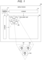
- Fig. 1 is a block diagram illustrating a configuration example of a display device 100 according to a first embodiment of the present technology.
- the display device 100 includes a control circuit 111, an H driver 112, a V driver 113, and a pixel array unit 120.
- a display integrated with an electronic device such as a smartphone or a personal computer, a monitor device separated from the electronic device, or the like is assumed.
- each of the pixels 200 includes a plurality of sub-pixels that emits light beams of mutually different colors.
- sub-pixels 201, 202, and 203 that emit R, G, and B light beams are disposed for every pixel 200.
- Each shape of the sub-pixels 201, 202, and 203 is a hexagonal shape, and these three are arranged in a triangular shape, for example. That is, the sub-pixels are arranged in a delta array. Note that a shape and an arrangement of the sub-pixels are not limited to the hexagonal shape and the delta array.
- the control circuit 111 controls a drive timing of each of the H driver 112 and the V driver 113 on the basis of image data.
- the H driver 112 drives the sub-pixels on a column basis.
- the V driver 113 drives the sub-pixels on a row basis.
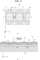
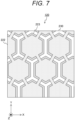
- Fig. 2 is an example of a plan view and a cross-sectional view of the pixel array unit 120 according to the first embodiment of the present technology.
- a is an example of a plan view of the pixel array unit 120
- b in the figure is an example of a cross-sectional view of the pixel array unit 120.
- the plurality of sub-pixels such as the sub-pixel 201 is arranged on a predetermined plane.
- a Z axis an axis perpendicular to the plane
- a predetermined axis parallel to the plane will be assumed as an "X axis”.
- An axis perpendicular to the X axis and the Z axis will be assumed as a "Y axis”.
- the X-axis direction can also be referred to as a "horizontal direction”.
- the Y-axis direction can also be referred to as a "vertical direction”.
- each of the sub-pixels has, for example, a hexagonal shape.
- a region surrounded by a one-dotted chain line in a of the figure indicates the sub-pixel 201.
- the plurality of sub-pixels is arranged at regular intervals.
- a region between the sub-pixels is hereinafter referred to as an "inter-pixel region".
- a region including a hatched portion and a white portion corresponds to the inter-pixel region.
- b illustrates a cross-sectional view of the pixel array unit 120 taken along a line segment between coordinates (X3, Y4) and (X8, Y4) in a of the figure.
- the pixel array unit 120 includes a substrate 240, protective films 211 and 212, a cathode electrode 221, an organic EL film 222, a plurality of anode electrodes 223, and an insulating film 230.
- the anode electrode 223 is formed for every sub-pixel.
- a direction from the substrate 240 to the anode electrode 223 is referred to as an "upper" direction.
- the individual anode electrodes 223 are separated (in other words, insulated) from each other by the insulating film 230 formed between the anode electrodes 223.
- the hatched portion corresponds to the anode electrode 223, and the white portion corresponds to the insulating film 230.
- the organic EL film 222 is formed above the anode electrode 223, and the cathode electrode 221 is formed above the organic EL film. Furthermore, the protective film 212 is formed above the cathode electrode 221, and the protective film 211 covering the protective film 212 and a portion between the pixels is formed above the protective film 212 and the portion between the pixels. Although the protective films 211 and 212 are separately formed in a manufacturing process described later, the protective films 211 and 212 are integrated and can be collectively treated as a protective film 210.
- a film thickness of a portion of the protective film 210 covering the sub-pixel is larger than a film thickness of other portion.
- the protective film 210 is raised at the portion of the sub-pixel.
- a low refractive index film (not illustrated) is filled. Therefore, light emitted from the sub-pixel is reflected upward by the side surface (in other words, a surface of the protective film) of the raised portion.
- a thick arrow in a of the figure indicates an optical path of light emitted by the sub-pixel.
- the protective films 211 and 212 and the cathode electrode 221 are omitted in order to clearly illustrate a planar shape of the organic EL film 222.
- a gray portion in a of the figure indicates the organic EL film 222.
- the organic EL film 222 is formed in each of the plurality of sub-pixels and in a portion mutually connecting adjacent sub-pixels in the inter-pixel region. In the inter-pixel region, a portion where the organic EL film 222 is formed is hereinafter referred to as a "connection portion".
- a rectangular portion of a dotted line surrounded by coordinates (X2, Y1), (X6, Y1), (X2, Y3), and (X6, Y3) in a of the figure corresponds to the connection portion.
- the anode electrode 223 is formed in a predetermined region surrounding the sub-pixel when viewed from the Z-axis direction.
- An outer periphery (coordinate X5, and the like) of a hatched portion in a of the figure corresponds to an outer periphery of the anode electrode 223.
- a planar shape of the cathode electrode 221 is similar to that of the organic EL film 222.
- an end portion of the insulating film 230 reaches an end portion of the anode electrode 223, and is raised by a thickness of the electrode.
- a hexagonal shape of a one-dotted chain line passing through the coordinate X4 and the like indicates an outer periphery of the raised portion of the insulating film 230. In the following figures, the one-dotted chain line is omitted.
- anode electrode 223 is an example of a first electrode described in the claims
- the cathode electrode 221 is an example of a second electrode described in the claims.
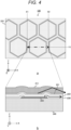
- Fig. 3 is an example of a plan view of the pixel array unit 120 and a cross-sectional view taken along a line segment including the connection portion according to the first embodiment of the present technology.
- a is an example of a plan view of the pixel array unit 120.
- b illustrates a cross-sectional view taken along a line segment between coordinates (X1, Y2) and (X7, Y2) in a of the figure. It is assumed that the line segment includes the connection portion between sub-pixels.
- the organic EL film 222 and the cathode electrode 221 are also formed in the connection portion, and adjacent sub-pixels are mutually connected by the organic EL film 222 and the cathode electrode 221.
- the organic EL film 222 is formed in each of the plurality of sub-pixels and a portion (that is, the connection portion) that mutually connects adjacent sub-pixels in the inter-pixel region between the sub-pixels, when viewed from the Z-axis direction. Furthermore, the organic EL film 222 is formed between the cathode electrode 221 and the anode electrode 223 when viewed from the Y-axis direction or the X-axis direction. Note that the cathode electrode 221 and the anode electrode 223 are examples of a first electrode and a second electrode described in the claims.
- the anode electrode 223 is formed for every sub-pixel in a predetermined region surrounding the sub-pixel when viewed from the Z-axis direction.
- the cathode electrode 221 is formed in each of the plurality of sub-pixels and in the connection portion when viewed from the Z-axis direction.
- a film thickness of a portion covering the sub-pixel in the protective film 210 is larger than a film thickness of other portion.
- a display device 100 having a structure in which the organic EL film 222 is formed over the entire inter-pixel region and the protective film is not raised in the portion of the sub-pixel is assumed as a comparative example.
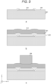
- Fig. 4 is an example of a plan view and a cross-sectional view of a pixel array unit 120 in the comparative example.
- a is an example of a plan view of the pixel array unit 120
- b of the figure is an example of a cross-sectional view taken along a line segment between coordinates (X1, Y1) and (X2, Y1) in a of the figure.
- the organic EL film 222 is formed on each of the sub-pixels and the entire inter-pixel region between the sub-pixels. This similarly applies to the cathode electrode 221. Furthermore, a film thickness of the protective film 211 is assumed to be substantially the same between a portion above the sub-pixel and a portion above the inter-pixel region.
- the leakage current can be made smaller than that in the comparative example in which the organic EL film 222 is formed in the entire region. Note that, in a configuration in which no organic EL film 222 is formed over the entire inter-pixel region, the organic EL film 222 and the cathode electrode 221 on the sub-pixel are isolated, and power cannot be supplied to each of the sub-pixels. In order to prevent this state, in Fig. 2 , the organic EL film 222 is left at the connection portion.
- the protective film 211 since the protective film 211 is not raised above the sub-pixel, light emitted from the sub-pixel may be reflected downward on a surface of the protective film.
- a thick arrow in the figure indicates an optical path of light reflected by the surface of the protective film.
- Fig. 5 is a diagram for explaining a manufacturing process up to photolithography according to the first embodiment of the present technology.
- a illustrates a cross-sectional view of the pixel array unit 120 in which the anode electrode 223 and the insulating film 230 are formed.
- b illustrates a cross-sectional view of the pixel array unit 120 in which the organic EL film 222, the cathode electrode 221, and the protective film 212 are formed.
- c illustrates a cross-sectional view of the pixel array unit 120 when photolithography is performed.
- a manufacturing system forms the anode electrode 223 for every sub-pixel on the substrate 240, and forms the insulating film 230 between the anode electrodes 223. Then, as exemplified in b of the figure, the manufacturing system forms the organic EL film 222 and the cathode electrode 221, and forms the protective film 212 on the cathode electrode 221. Subsequently, the manufacturing system disposes a photoresist 250 on each of the sub-pixels, and performs photolithography.
- Fig. 6 is a diagram for explaining a manufacturing process up to film formation of the protective film 211 according to the first embodiment of the present technology.
- a illustrates a cross-sectional view of the pixel array unit 120 after photolithography.
- b illustrates a cross-sectional view of the pixel array unit 120 on which the protective film 211 is formed.
- the protective film 212 above the sub-pixel is left, the protective film 212 of other portion is removed by photolithography. Then, as exemplified in b of the figure, the manufacturing system forms the protective film 211. As a result, the pixel array unit 120 having the structure exemplified in Fig. 2 is obtained.
- Fig. 2 sub-pixels arranged in an oblique direction and the horizontal direction (X-axis direction) are mutually connected by the organic EL film 222, but the present technology is not limited to this configuration.
- connection portions in the horizontal direction can be reduced, to mutually connect only sub-pixels arranged in the oblique direction.
- connection portions in the oblique direction it is also possible to reduce the number of connection portions in the oblique direction, to mutually connect only sub-pixels arranged in the horizontal direction.
- connection portions in the horizontal direction and the oblique direction it is also possible to reduce the number of connection portions in the horizontal direction and the oblique direction, provide connection portions in a vertical direction (Y-axis direction), to mutually connect sub-pixels arranged in the vertical direction.
- connection portions in the vertical direction may be added, to mutually connect sub-pixels arranged in the horizontal direction, the vertical direction, and the oblique direction.
- connection portions in the oblique direction it is also possible to reduce the number of connection portions in the oblique direction and add the connection portions in the horizontal direction, to mutually connect sub-pixels arranged in the horizontal direction and the vertical direction.
- the sub-pixels are arranged in a delta array, but the present technology is not limited to this configuration.
- the sub-pixels may have a square shape, and may be arranged in a square array.
- connection portions may be provided in the oblique direction to mutually connect sub-pixels arranged in the oblique direction.
- connection portions may be provided in the vertical direction to mutually connect sub-pixels arranged in the vertical direction.
- connection portions may be provided in the horizontal direction to mutually connect sub-pixels arranged in the horizontal direction.
- connection portions may be provided in the horizontal direction and the vertical direction, to mutually connect sub-pixels arranged in the horizontal direction and the vertical direction.
- connection portions may be provided in the horizontal direction, the vertical direction, and the oblique direction, to mutually connect sub-pixels arranged in the horizontal direction, the vertical direction, and the oblique direction.
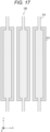
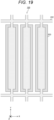
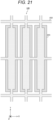
- the sub-pixel may have a rectangular shape, and may be arranged in a stripe array.
- connection portions may be provided in the vertical direction to mutually connect sub-pixels arranged in the vertical direction.
- connection portions may be provided in the horizontal direction to mutually connect sub-pixels arranged in the horizontal direction.
- sub-pixels arranged in the vertical direction may be mutually connected, and further, the connection portions arranged in the horizontal direction may be mutually connected.
- connection portions may be provided in the horizontal direction and the vertical direction, to mutually connect sub-pixels arranged in the horizontal direction and the vertical direction.
- sub-pixels arranged in the horizontal direction and the vertical direction may be mutually connected, and the connection portions arranged in the horizontal direction may be mutually connected.
- the connection portion in the inter-pixel region is used as the connection portion, but the present technology is not limited to this configuration.
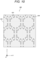
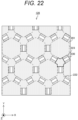
- the organic EL film 222 can also be formed by using, as the connection portion, a portion other than the rectangular portion in the inter-pixel region between the adjacent sub-pixels.
- a Y-shaped portion surrounded by a thick dotted line corresponds to the connection portion.
- a part of the anode electrode 223 and a part of the insulating film 230 are disposed in the rectangular portion.
- the organic EL film 222 is formed in each of the sub-pixels and the connection portion in the inter-pixel region, it is possible to reduce the leakage current as compared with the case where the organic EL film 222 is formed in the entire inter-pixel region.
- the film thickness of the portion covering the sub-pixel in the protective film 210 is made larger than the film thickness of the other portion, the light extraction efficiency can be improved.
- a width of each cathode electrode 221 of the connection portion in the pixel array unit 120 is constant, but it is difficult to suppress shading in this configuration.
- a display device 100 according to a second embodiment is different from that of the first embodiment in that a width of a cathode electrode 221 is changed according to a distance from a central portion.
- Fig. 23 is an example of a plan view of a pixel array unit 120 according to the second embodiment of the present technology.
- the pixel array unit 120 of the second embodiment is different from that of the first embodiment in that a width of the cathode electrode 221 of a connection portion between sub-pixels is smaller as being closer to a central portion.
- a potential drop (in other words, IR drop) occurs due to resistance of the cathode electrode 221, and a potential difference between an anode and a cathode in individual pixels decreases.
- a cathode contact electrode (not illustrated) that supplies a potential to the cathode electrode 221 is disposed in a periphery of the pixel array unit 120. Therefore, as being farther from the periphery, in other words, as being closer to a center of the pixel array unit 120, a potential difference becomes smaller, a current flowing through an organic EL film 222 decreases, and luminance decreases. As a result, luminance becomes non-uniform, and shading may occur.
- the width of the cathode electrode 221 By setting the width of the cathode electrode 221 to be narrower as being closer to the central portion, an area of side-wall reflection exemplified in Fig. 2 is increased as being closer to the center, and the light extraction efficiency is improved. Therefore, it is possible to suppress a decrease (that is, shading) in luminance in the central portion.
- the width of the cathode electrode 221 of the connection portion is set to a value according to a distance from the central portion, shading can be suppressed.
- the width of the connection portion of the organic EL film 222 is constant. However, in this configuration, it is necessary to shift a position of a lens to change a direction of a principal ray when principal ray control is performed.
- a display device 100 according to a third embodiment is different from that of the first embodiment in that the principal ray control is realized by setting a width of one end of a connection portion to a value different from that of another end.
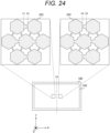
- Fig. 24 is an example of a plan view of a delta-array pixel array unit 120 according to the third embodiment of the present technology.
- a width of one end of a connection portion of an organic EL film 222 is different from that of another end.
- a width of one end farther from a central portion of the pixel array unit 120 out of both ends of the connection portion is assumed to be wider than a width of another end.
- the width gradually changes from one end to another end.
- an X coordinate of the central portion of the pixel array unit 120 is assumed to be X3.
- a width of a left end at the coordinate X1 or the like is wider than a width of a right end at the coordinate X2 or the like.
- a width of a left end at the coordinate X4 or the like is narrower than a right end at the coordinate X5 or the like.
- a width of an upper end of the connection portion is wider than a width of a lower end.
- a width of an upper end of the connection portion is narrower than a width of a lower end.
- the principal ray can be directed toward the center without shifting a position of a lens.
- this principal ray control light can be collected at the central portion of the display device 100. Note that, in the figure, the connection portion on the upper side and the lower side of the central portion is omitted.
- the width of the connection portion may simply be increased as the distance from the central portion increases.
- An X coordinate of the central portion is assumed to be X5. On a left side of the coordinate X5, a width of a left end at the coordinate X1 of a certain connection portion is wider than a width of a right end at the coordinate X2.
- a width of a left end at the coordinate X3 of a connection portion closer to the central portion than the certain connection portion is wider than a width of a right end at the coordinate X4, and widths of the coordinates X3 and X4 are narrower respectively than widths of the coordinates X1 and X2.
- a width of a left end at the coordinate X6 of a certain connection portion is narrower than a right end at the coordinate X7.
- a width of a left end at the coordinate X8 of a connection portion farther from the central portion than the certain connection portion is narrower than a right end at the coordinate X9, and widths at coordinates X8 and X9 are respectively wider than widths at coordinates X6 and X7.
- the width of the connection portion becomes wider as being closer to an upper end of the pixel array unit 120.
- the width of the connection portion becomes wider as being closer to a lower end of the pixel array unit 120.
- a width of one end of the connection portion can be set to a value different from that of another end.
- the width of the connection portion can be changed according to a distance from the central portion in the square array.
- connection portion can be formed in a T shape.
- the principal ray control can be performed without shifting the position of the lens.
- connection portion In the first embodiment described above, adjacent sub-pixels are mutually connected by the connection portion. However, if the connection portion is too thin, the connection portion may be broken and the sub-pixel may be become a black spot due to a connection failure.
- a display device 100 according to a fourth embodiment is different from that of the first embodiment in that a connection failure is prevented.
- Fig. 29 is an example of a plan view of a pixel array unit 120 according to the fourth embodiment of the present technology.
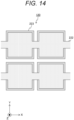
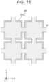
- the pixel array unit 120 of the fourth embodiment is different from that of the first embodiment in that, in a case where attention is paid to a pair of adjacent sub-pixels, the sub-pixels are connected by two connection portions. In the figure, a portion surrounded by a thick dotted line corresponds to the connection portion.
- a pair of adjacent sub-pixels can be connected by three or more sub-pixels.
- the connection between the sub-pixels can be maintained by the remaining connection portions. As a result, a connection failure can be prevented.
- connection portions between the pair of sub-pixels are examples of first and second connection portions described in the claims.
- connection failure can be prevented.
- connection portions is increased to two or more. However, even with this configuration, connection failure may not be sufficiently prevented.
- a display device 100 in a modification of the fourth embodiment is different from that of the fourth embodiment in that an edge of a connection portion has an arc shape.
- Fig. 30 is an example of a plan view of a pixel array unit 120 according to the modification of the fourth embodiment of the present technology.
- the pixel array unit 120 according to the modification of the fourth embodiment is different from that of the fourth embodiment in that there is one connection portion between a pair of adjacent sub-pixels and an edge of the connection portion has an arc shape.
- the edge of the connection portion has, for example, an arc shape of a fan.
- a region surrounded by a thick dotted line in the figure corresponds to the connection portion.
- a Y-shaped connection portion may be disposed in the vicinity of a vertex of a hexagonal sub-pixel, and an edge of the connection portion may have an arc shape.
- a region surrounded by a thick dotted line in the figure corresponds to the connection portion.
- connection portions can be provided between a pair of sub-pixels.
- connection failure can be prevented.
- connection portion has a rectangular shape.
- a display device 100 according to a fifth embodiment is different from that of the first embodiment in that a width of a center of a connection portion is increased to improve the light extraction efficiency.
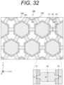
- Fig. 32 is an example of a plan view of a pixel array unit 120 according to the fifth embodiment of the present technology.
- the pixel array unit 120 of the fifth embodiment is different from that of the first embodiment in that a width of a center of the connection portion is wider than widths of both ends of the connection portion.
- hexagonal sub-pixels 201 and 202 are arranged in the X-axis direction, an X coordinate of a right end of the sub-pixel 201 is assumed to be X1, an X coordinate of a left end of the sub-pixel 202 on a right side thereof is assumed to be X3, and the X coordinate in a middle thereof is assumed to be X2.
- the X coordinates of the left end and the right end of the connection portion connecting the sub-pixels correspond to X1 and X3, and the X coordinate of the center corresponds to X2.
- lengths (that is, widths) of the connection portion at the coordinates X1 and X3 in the Y-axis direction are assumed to be Y1 and Y3
- a width of the connection portion at the coordinate X2 is assumed to be Y2
- Y2 is larger than each of Y1 and Y3.
- the width of the center of the connection portion is widened, the light extraction efficiency can be improved.
- a display device 100 in a first modification of the fifth embodiment is different from that of the fifth embodiment in that a central portion of a connection portion is opened.
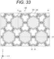
- Fig. 33 is an example of a plan view of a pixel array unit 120 in the first modification of the fifth embodiment of the present technology.
- the first modification of the fifth embodiment is different from the fifth embodiment in that a part of the central portion of the connection portion of the pixel array unit 120 is opened, and an organic EL film 222 is not formed in the opened region.
- a thick rectangle between the coordinates X2 and X3 indicates the opened region.
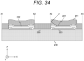
- Fig. 34 is a cross-sectional view taken along a line segment between coordinates (X1, Y2) and (X4, Y2) in Fig. 33 .
- the light extraction efficiency can be further improved.
- connection portions may be mutually connected.
- a display device 100 in a second modification of the fifth embodiment is different from that of the fifth embodiment in that adjacent connection portions are mutually connected.
- Fig. 35 is an example of a plan view of a pixel array unit 120 in the second modification of the fifth embodiment of the present technology.
- the organic EL film 222 is also formed in a region extending from a central portion of a connection portion along an edge of a sub-pixel, and adjacent sub-pixels are mutually connected.
- a region where the sub-pixels are mutually connected is hereinafter referred to as a "bridge portion".
- a Y-shaped region surrounded by a thick dotted line at the same time indicates the bridge portion.
- the organic EL film 222 is formed in the hexagonal sub-pixel, the connection portion mutually connecting the sub-pixels, and the bridge portion mutually connecting the connection portions.
- Fig. 36 is a cross-sectional view taken along a line segment between coordinates (X1, Y2) and (X2, Y2) in Fig. 35 .
- connection portion As the width of the connection portion is made narrower, resistance of a cathode electrode 221 above the connection portion becomes larger. However, as exemplified in Figs. 35 and 36 , by mutually connecting the connection portions by using the bridge portion, the resistance of the cathode electrode 221 can be reduced by the increased amount. This configuration makes it possible to suppress an increase in resistance of the cathode electrode 221 when the width of the connection portion is narrowed.
- the organic EL film 222 is also formed in the bridge portion mutually connecting the connection portions, an increase in the resistance of the cathode electrode 221 can be suppressed.
- a display device 100 according to a sixth embodiment is different from that of the first embodiment in that the light extraction efficiency is improved by providing unevenness on a side wall of a sub-pixel when viewed from the Z-axis direction.
- Fig. 37 is an example of a plan view of a pixel array unit 120 according to the sixth embodiment of the present technology.
- a is an example of a plan view when viewed from the Z-axis direction without an on-chip lens 261 and a color filter 262
- b of the figure is an example of a plan view when three sub-pixels are viewed from the Z-axis direction.
- a portion of the sub-pixel protruding from the side surface is referred to as a "protrusion”, and a portion other than the protrusion is referred to as a "core portion”.
- the planar shape of the sub-pixel viewed from the Z-axis direction can be expressed as a figure in which the core portion and the plurality of protrusions are combined.
- the shape of the sub-pixel corresponds to a shape of each of an organic EL film 222 excluding a connection portion, a cathode electrode 221, and a protective film 211. Furthermore, adjacent sub-pixels are connected to each other by the connection portion in an oblique direction.
- a portion surrounded by a thick dotted line in a of the figure corresponds to the core portion.
- the sub-pixel has a shape (in other words, a cross shape) in which the core portion is rectangular and a rectangular protrusion is adjacent to each of four edges of the core portion.
- the on-chip lens 261 and the color filter 262 are provided in each of the sub-pixels 201 to 203.
- a circular line indicates an outer periphery of the on-chip lens 261
- a rectangular thick frame indicates an outer periphery of the color filter 262.
- the connection portion is omitted.
- Fig. 38 is an example of a cross-sectional view of the pixel array unit 120 according to the sixth embodiment of the present technology. This figure is an example of a cross-sectional view taken along a line segment Xa-Xb in the horizontal direction including the core portion in b of Fig. 37 . Furthermore, a thick dotted line in Fig. 38 indicates a cross-sectional shape of the protrusion taken along a line segment Xc-Xd including only the protrusion out of the core portion and the protrusion in b of Fig. 37 . Furthermore, an arrow indicates an optical path of light emitted by the organic EL film 222. By providing unevenness on the side wall, the protrusion functions as a light guide, and the light extraction efficiency can be improved.
- the cross section taken along the line segment Xa-Xb in the horizontal direction does not include the connection portion. Adjacent sub-pixels in this cross section are separated from each other by the insulating film 230. Furthermore, a low refractive index film 270 is formed below the color filter 262.
- Fig. 39 is an example of a cross-sectional view taken along a line segment including the connection portion according to the sixth embodiment of the present technology.
- This figure is an example of a cross-sectional view taken along a line segment Xe-Xf in the oblique direction in a of Fig. 37 .
- the cross section taken along the line segment Xe-Xf in the oblique direction includes the connection portion.
- the adjacent sub-pixels are connected to each other by the connection portion.
- Fig. 40 is a diagram for explaining a manufacturing process of the display device 100 according to the sixth embodiment of the present technology.
- a illustrates a cross-sectional view before photolithography
- b illustrates a cross-sectional view after photolithography.
- a manufacturing system forms the organic EL film 222 and the cathode electrode 221, then forms the protective film 211 on the organic EL film and the cathode electrode, and disposes a photoresist 250 on the protective film.
- a shape of the photoresist 250 as viewed from the Z-axis direction is a shape obtained by hollowing out the connection portion and the sub-pixel having unevenness.
- the manufacturing system performs photolithography.
- the protective film 211 is processed into a shape having unevenness.
- b illustrates a cross section taken along the line segment Xa-Xb in Fig. 37 .
- Fig. 41 is a diagram illustrating an example of a shape of a sub-pixel having four protrusions according to the sixth embodiment of the present technology.
- the core portion has a rectangular shape
- the protrusion may also have a triangular shape.
- the protrusion may also be formed in a rectangular shape, and the protrusion may also be disposed adjacent to a vertex of the core portion.
- the protrusion may also be formed in a rectangular shape and disposed adjacent to four edges of the core portion.
- the protrusion may be a semicircle.
- the protrusion may be a wedge.
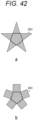
- Fig. 42 is a diagram illustrating an example of a shape of a sub-pixel having five protrusions according to the sixth embodiment of the present technology.
- the core portion has a pentagonal shape
- up to five protrusions can be provided.
- the protrusion may also have a triangular shape.
- the protrusion may have a rectangular shape.
- Fig. 43 is a diagram illustrating an example of a shape of a sub-pixel having six protrusions according to the sixth embodiment of the present technology.
- the core portion has a hexagonal shape
- up to six protrusions can be provided.
- the protrusion may also have a triangular shape.
- the protrusion may have a rectangular shape.
- the protrusion may have a hexagonal shape.
- Fig. 44 is a diagram illustrating an example of a shape of a sub-pixel having eight protrusions according to the sixth embodiment of the present technology.
- the core portion has an octagonal shape
- up to eight protrusions can be provided.
- the protrusion may also have a triangular shape.
- the protrusion may have a rectangular shape.
- the number of protrusions can be set to nine or more.
- the number of protrusions is increased, there is a higher possibility that a resolution limit of lithography is exceeded, and the function of the protrusions as light guides is deteriorated as the shape is closer to a circular shape. For this reason, the cases where the number of protrusions is four to eight, which are highly practical, have been exemplified.
- connection portions are disposed only in the oblique direction, the connection portions may also be disposed in the vertical direction and the horizontal direction as described above.
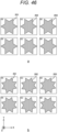
- sub-pixels can be arranged in a stripe array.
- the connection portion is omitted.
- the number of protrusions can be four.
- the number of protrusion can be five.
- the number of protrusion can be six.
- the number of protrusion can be eight.
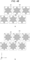
- sub-pixels can be arranged in a delta array.
- the connection portion is omitted.
- the number of protrusions can be four.
- the number of protrusion can be five.
- the number of protrusion can be six.
- the number of protrusion can be eight.
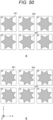
- the sub-pixels can be arranged in a square array.
- the connection portion is omitted.
- the number of protrusions can be four.
- the number of protrusion can be five.
- the number of protrusion can be six.
- the number of protrusion can be eight.
- the shape of the sub-pixel as viewed from the Z-axis direction is a figure in which the core portion and the plurality of protrusions are combined, the light extraction efficiency can be improved.
- the shape of the organic EL film 222 in the sub-pixel is a hexagonal shape when viewed from the Z-axis direction, but it is difficult to further improve the light extraction efficiency with this shape.
- a display device 100 according to a seventh embodiment is different from that of the first embodiment in that a bent portion is provided in an organic EL film 222 to improve the light extraction efficiency.
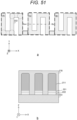
- Fig. 51 is a view illustrating a plan view of the organic EL film 222 and a cross-sectional view of a pixel array unit 120 according to the seventh embodiment of the present technology.
- a illustrates a plan view of the organic EL film 222 as viewed from the Z-axis direction.
- b illustrates a cross-sectional view taken along a line segment Xa-Xb in a of the figure.
- the organic EL film 222 has a shape having a predetermined number of bent portions when viewed from the Z-axis direction.
- a rough dotted line indicates an outer periphery of a sub-pixel
- a fine rectangular dotted line indicates an outer periphery of a connection portion.
- a circular dotted line indicates a bent portion.
- the organic EL film 222 in the sub-pixel is bent in an S shape at a right angle at each of four bent portions.
- an upper surface of an anode electrode 223 below the organic EL film 222 is not processed into the shape having the bent portion.
- shapes of a cathode electrode 221 and a protective film 211 stacked on the organic EL film 222 as viewed from the Z-axis direction are assumed to be the same as that of the organic EL film 222.
- Fig. 52 is a diagram for explaining a manufacturing process up to photolithography according to the seventh embodiment of the present technology.
- a illustrates a cross-sectional view of the pixel array unit 120 when the protective film 211 is formed.
- b illustrates a cross-sectional view of the pixel array unit 120 when photolithography is performed.
- the protective film 211 that covers the top of the cathode electrode 221 is formed for every sub-pixel.
- the organic EL film 222 is not processed into the pattern such as the S shape having the bent portion.
- the manufacturing system disposes a photoresist 250 above each of the sub-pixels, and performs photolithography.
- the photoresist 250 has a shape obtained by hollowing out a pattern such as an S shape when viewed from the Z-axis direction.
- Fig. 53 is a diagram for explaining a manufacturing process up to film formation of a low refractive index film 270 according to the seventh embodiment of the present technology.
- a illustrates a cross-sectional view of the pixel array unit 120 after photolithography.
- b illustrates a cross-sectional view of the pixel array unit 120 on which the low refractive index film 270 is formed.
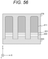
- the protective film 211, the cathode electrode 221, and the organic EL film 222 are processed into a shape having a bent portion when viewed from the Z-axis direction by photolithography. Then, as exemplified in b of the figure, the manufacturing system performs embedding with the low refractive index film 270 to cover a processed end surface. The processed end surface of the organic EL film 222 is embedded and covered with the low refractive index film 270 to form a reflection interface. The light extraction efficiency can be improved by increasing a reflection area of a side wall.
- the low refractive index film 270 for example, a transparent material such as silicon nitride (SiN x ), silicon dioxide (SiO 2 ), lithium fluoride (LiF), magnesium fluoride (MgF), or silicon oxynitride (SiON) is used.
- the low refractive index film 270 may be a porous film (having a low film density), and a film having a lower refractive index of 1.4 or less can be obtained by, for example, using SiO x as the porous film.
- the low refractive index film 270 may be formed as a low refractive index portion inside the protective film 211 on an end surface, and includes a gap and an air gap.
- the side wall By forming a refractive index difference interface by using the low refractive index film 270, light emitted from the organic EL film 222 is reflected by the side wall, and the light extraction efficiency can be improved.
- the side-wall reflection area increases not only in a peripheral portion of the sub-pixel but also inside the sub-pixel. As a result, the light extraction efficiency can be further enhanced.
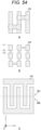
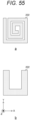
- Fig. 54 is a view illustrating an example of a plan view of the organic EL film 222 according to the seventh embodiment of the present technology.
- a shape of the organic EL film 222 viewed from the Z-axis direction is not limited to the above-described S shape as long as a predetermined number of bent portions are provided.
- a shape (so-called ghost Leg shape) may be adopted in which a horizontal line is drawn between a plurality of parallel lines in a direction vertical to the parallel lines.
- a width of a part of the organic EL film 222 may have a shape different from a width of other portion.
- a width of a portion between the coordinates Y1 and Y2 is formed to be wider than a width of a portion between the coordinates Y2 to Y3.
- the organic EL film 222 may have a shape in which a plurality of notches is formed (so-called comb shape).
- c illustrates a shape of adjacent sub-pixels 201 and 202.
- the organic EL film 222 may have a spiral shape. Furthermore, as exemplified in b of the figure, the organic EL film 222 may have a U shape. Furthermore, it is also possible to perform rotation by 90 degrees or reverse arrangement. An orientation of the sub-pixel can be changed for every color. Furthermore, an arrangement angle can be changed toward an outer peripheral portion of the pixel array unit 120.
- anode electrode 223 is not processed into the pattern having the bent portion, but is not limited to this configuration.
- the anode electrode 223 can be processed into the same shape (S shape or the like) as those.
- sub-pixels having the shape having the bent portion can be arranged in a stripe array.
- sub-pixels may be arranged in a delta array.
- sub-pixels can be arranged in a square array.
- two B sub-pixels may also be disposed adjacent to each other in pixels in which two rows ⁇ two columns are disposed.
- the two B sub-pixels may be arranged in an oblique direction.
- the organic EL film 222 in the sub-pixel has a shape having a predetermined number of bent portions, the light extraction efficiency can be improved.
- a display device 100 according to an eighth embodiment is different from that of the first embodiment in that unevenness is formed on a side wall of a sub-pixel when viewed from the X-axis direction or the Y-axis direction to prevent color mixing and improve the light extraction efficiency.
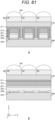
- Fig. 61 is a diagram illustrating an example of a cross-sectional view of a pixel array unit 120 according to the eighth embodiment of the present technology.
- a is an example of a cross-sectional view of the pixel array unit 120 taken along a cross section not including a connection portion.
- b is an example of a cross-sectional view of the pixel array unit 120 taken along a cross section including a connection portion.
- an organic EL film 222, a cathode electrode 221, and a protective film 212 are stacked on an anode electrode 223 in each of red (R), green (G), and blue (B) sub-pixels. Furthermore, a protective film 211 is formed so as to cover a side surface of each of the organic EL film 222 and the cathode electrode 221 and a side surface and the top of the protective film 212. Furthermore, embedding is performed with a low refractive index film 270 between individual sub-pixels, and a color filter 262 and an on-chip lens 261 are formed thereon.
- unevenness is formed on a side wall of the protective film 211, in other words, a side wall of the sub-pixel when viewed from the X-axis direction or the Y-axis direction. Due to the formation of the unevenness, side-wall reflection of each of the sub-pixels is enhanced as compared with a case where there is no unevenness, and an amount of light incident on the color filter 262 immediately above is increased while maintaining a sealing property. As a result, color mixing can be prevented, and the light extraction efficiency can be improved.
- a cross-sectional shape of a protrusion in the unevenness has, for example, a rectangular shape.
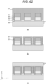
- Fig. 62 is a diagram for explaining a manufacturing process according to the eighth embodiment of the present technology.
- the manufacturing system forms the anode electrode 223, the organic EL film 222, the cathode electrode 221, and the protective film 212 for every sub-pixel on a substrate 240, and performs embedding with the protective film 211.
- a refractive index of the protective film 211 is a value lower than or equal to a refractive index of the protective film 212 on the sub-pixel.
- the manufacturing system forms unevenness on the side wall of the protective film 211 by dry etching again, and performs embedding with the low refractive index film 270 as exemplified in c of the figure.
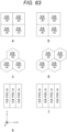
- Fig. 63 is a diagram illustrating an example of an arrangement method for sub-pixels according to the eighth embodiment of the present technology.
- the sub-pixels are arranged in a square array.
- sub-pixels of R, G, and B may be arranged as exemplified in a of the figure, or sub-pixels of R, G, B, and W (white) may be arranged as exemplified in b of the figure.
- the sub-pixels may be arranged in a delta array.
- sub-pixels of R, G, and B may be arranged as exemplified in c of the figure, or sub-pixels of R, G, B, and W may be arranged as exemplified in d of the figure.
- the sub-pixels may be arranged in a stripe array.
- sub-pixels of R, G, and B may be arranged as exemplified in e of the figure, or sub-pixels of R, G, B, and W may be arranged as exemplified in f of the figure.
- a cathode contact electrode 224 may also be disposed between adjacent pixels.
- the unevenness is formed on the side wall of the sub-pixel when viewed from the X-axis direction or the Y-axis direction, color mixing can be prevented, and the light extraction efficiency can be improved.
- the unevenness is formed on the side wall of the protective film 211 of each sub-pixel, but the unevenness may be formed other than the protective film 211.
- a display device 100 according to a first modification of the eighth embodiment is different from that of the eighth embodiment in that a texture film is added and unevenness is formed on the texture film.
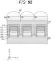
- Fig. 65 is a diagram illustrating an example of a cross-sectional view of a pixel array unit 120 according to the first modification of the eighth embodiment of the present technology.
- An upper surface and a side surface of the protective film 211 of each of sub-pixels of the first modification of the eighth embodiment are covered with a texture film 215. Unevenness is formed on the texture film 215 instead of the protective film 211.
- zinc oxide (ZnO) is used as the texture film 215.
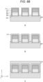
- Fig. 66 is a diagram for explaining a manufacturing process in the first modification of the eighth embodiment of the present technology.
- embedding with the protective film 211 is not performed.
- the manufacturing system forms the texture film 215 having unevenness, on the upper surface and the side surface of the protective film 211.
- the manufacturing system embeds the sub-pixels with the low refractive index film 270.
- an air gap surrounded by the texture film 215 can also be formed between the sub-pixels.
- the unevenness is formed in the texture film 215, light is reflected by the side wall to prevent color mixing, and the light extraction efficiency can be improved.
- the unevenness is formed on the entire side wall of the sub-pixel, but the unevenness may be formed only on a part of the side wall.
- a display device 100 according to a second modification of the eighth embodiment is different from that of the eighth embodiment in that unevenness is formed on an upper portion and a lower portion of the side wall.
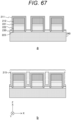
- Fig. 68 is a diagram illustrating an example of a cross-sectional view of a pixel array unit 120 according to the second modification of the eighth embodiment of the present technology.
- the pixel array unit 120 according to the second modification of the eighth embodiment is different from that of the eighth embodiment in that unevenness is formed only on the upper portion of the side wall of the protective film 210.
- Fig. 69 is a diagram for explaining a manufacturing process in the second modification of the eighth embodiment of the present technology.
- the manufacturing system forms the organic EL film 222, and forms a layer of the cathode electrode 221 on the organic EL film 222.
- the organic EL film 222 and the cathode electrode 221 are not separated for every sub-pixel.
- the protective film 212 is formed by stacking a plurality of layers having different etching rates at the time of etching on the cathode electrode 221. For example, a layer 212-1 having a higher etching rate and a layer 212-2 having a lower etching rate are alternately stacked.
- the manufacturing system separates the protective film 212 for every sub-pixel by dry etching, and forms unevenness on the side wall of the protective film 211 by wet etching using an etching rate difference, as exemplified in c of the figure.
- the manufacturing system separates the protective film 211, the organic EL film 222, and the cathode electrode 221 for every sub-pixel by dry etching, and further forms the protective film 212 on the top and a side surface of each of the separated portions.
- unevenness is formed only on the upper portion of the side wall of the protective film 210 including the protective films 211 and 212.
- unevenness may be formed only in a lower portion of the side wall.
- the cross-sectional shape of the protrusion of the unevenness of the side wall is rectangular, but the cross-sectional shape of the protrusion is not limited to rectangular.
- a display device 100 in a third modification of the eighth embodiment is different from that of the eighth embodiment in that the cross-sectional shape of unevenness is changed.
- Fig. 71 is a diagram illustrating an example of a cross-sectional view of a pixel array unit 120 according to the third modification of the eighth embodiment of the present technology.
- a illustrates an example of a cross-sectional view of the pixel array unit in which the cross-sectional shape of the protrusion is triangular.
- b illustrates an example of a cross-sectional view of the pixel array unit 120 in which the cross-sectional shape of the recess is semicircular.
- the cross-sectional shape of the protrusion can be made triangular.
- the cross-sectional shape of the recess can be made semicircular.
- any shape can be selected as the cross-sectional shape of the unevenness of the side wall, including the above-described triangular and the like.
- the unevenness is constituted by a polygon including a plurality of vertices of the protrusions, and the cross-sectional shape of the protrusion includes at least one of a triangle, a quadrangle, a polygon, or a circle, and may partially include a curve.
- emission intensity is improved at any viewing angle by introducing the uneven shape.
- the emission intensity increases depending on a depth and a width of the recess, for example. In a case where the depth is 200 nanometers (nm) and the width is 120 nanometers (nm), the emission intensity is 1.21 times as large as that in a case where there is no unevenness.
- the light extraction efficiency can be adjusted.
- a fourth modification of the eighth embodiment is different from the eighth embodiment in that a gap is provided between sub-pixels.
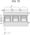
- Fig. 72 is a diagram illustrating an example of a cross-sectional view of a pixel array unit 120 according to the fourth modification of the eighth embodiment of the present technology.
- a gap surrounded by the protective film 211 is provided between sub-pixels.
- the low refractive index film 270 is laminated on the protective film 211. The light extraction efficiency can be adjusted by changing reflectance of side reflection by the gap.
- the light extraction efficiency can be adjusted.
- the organic EL film 222 is formed in the sub-pixel and in the connection portion between the sub-pixels when viewed from the Z-axis direction.
- this layout when a portion where the organic EL film 222 is not formed is set as an opening, and an angle formed by edges of the opening is small, there is a possibility that coverage of the protective film 211 of the side wall is deteriorated and a moisture entry path occurs.
- a display device 100 according to a ninth embodiment is different from that of the first embodiment in that an organic EL film 222 is formed in a layout in which an angle formed by edges of an opening is large.
- Fig. 73 is a plan view illustrating an example of a layout of the organic EL film 222 according to the first embodiment of the present technology.
- a of the figure illustrates a layout of the organic EL film 222 according to the first embodiment when viewed from the Z-axis direction.
- the organic EL film 222 is formed in a predetermined number of sub-pixels, a connection portion between the sub-pixels, and a frame-shaped frame 222-1 surrounding the sub-pixels.
- a circular region indicates the sub-pixel, and a rectangular portion mutually connecting circles indicates the connection portion.
- a dotted line indicates a boundary of the frame 222-1.
- the boundary of the frame 222-1 is a straight line, and some sub-pixels are cut by the boundary.
- a plurality of openings is formed in the organic EL film 222. These openings are divided into an opening 281 having at least one edge in contact with the frame 222-1 and an opening 282 having no edge in contact with the frame 222-1.
- b illustrates an enlarged view of the opening 281.
- a thick line in b of the figure indicates a boundary of the opening 281.
- the boundary includes a linear edge and an arc.
- An angle between two edges is, for example, 120° or 30°.
- c illustrates an enlarged view of the opening 282.
- a thick line in c of the figure indicates a boundary of the opening 282. This boundary also includes a linear edge and an arc. An angle between two edges is, for example, 60° or 120°.
- Fig. 74 is an example of a perspective view of an opening according to the first embodiment of the present technology.
- a indicates a smallest angle among angles formed by two edges of the opening 281 having at least one edge in contact with the frame 222-1, and the angle is 30°.
- b indicates a smallest angle among angles formed by two edges of the opening 282 having no edge in contact with the frame 222-1, and the angle is 60°.
- a minimum value of angles formed by two edges of the opening 281 is smaller than that of the opening 282.
- the coverage of a protective film 211 (silicon nitride or the like) on the side wall of the organic EL film 222 is deteriorated, and a thin portion of a protective film 221 is generated. This portion is likely to be an entry path of moisture. When moisture enters, damage may be formed on the organic EL film 222, causing deterioration of the organic EL film.
- Fig. 75 is a plan view illustrating an example of a layout of the organic EL film 222 according to the ninth embodiment of the present technology.
- the organic EL film 222 is also formed at a portion that has been the opening 281 in the first embodiment.
- a boundary of the frame 222-1 indicated by a dotted line has a sawtooth shape.
- a shape of an opening 281-1 in contact with at least one edge of the frame 222-1 having this shape is the same as the shape of the opening 282 having no edge in contact with the frame 222-1.
- the opening 281-1 is an example of a first opening described in the claims
- the opening 282 is an example of a second opening described in the claims.
- a minimum value of angles formed by two edges of the opening 282-1 is equal to a minimum value of angles formed by two edges of the opening 282.
- a film thickness of the protective film 211 in the vicinity of the frame 222-1 can be made equal to that of a side surface of a sub-pixel away from the frame 222-1, and deterioration of the frame 222-1 can be avoided.
- an aspect ratio of the opening is further increased, and the coverage of the protective film 211 is deteriorated. Therefore, it is important to avoid deterioration by the layout exemplified in the figure.
- a minimum value of angles formed by two edges of an opening having at least one edge in contact with the frame 222-1 can also be made larger than a minimum value of angles formed by two edges of an opening having no edge in contact with the frame 222-1.
- each of the second to eighth embodiments can be applied to the ninth embodiment.
- the shape of the opening 281-1 having at least one edge in contact with the frame 222-1 is the same as that of the opening 282 having no such an edge, but the present technology is not limited to this layout.
- a display device 100 in a first modification of the ninth embodiment is different from that of the ninth embodiment in that a layout is changed.
- Fig. 76 is a plan view illustrating an example of a layout of the organic EL film 222 in the first modification of the ninth embodiment of the present technology.
- a boundary of the frame 222-1 includes an edge having a sawtooth shape and an edge having a linear shape.
- the opening 281-1 in contact with the former has the same shape as the opening 282.
- an opening 281-2 in contact with the latter is different in shape from the opening 282, and has a shape close to a triangular shape.
- b illustrates an enlarged view of the opening 281-2.
- a minimum value of angles formed by two edges of the opening 281-2 is 60°.
- a minimum value of angles formed by two edges is equal to a minimum value of angles formed by two edges of the opening 282. Therefore, deterioration of the frame 222-1 can be suppressed.
- the shape of the opening 281-1 having at least one edge in contact with the frame 222-1 is the same as that of the opening 282 having no such an edge, but the present technology is not limited to this layout.
- a display device 100 in a second modification of the ninth embodiment is different from that of the ninth embodiment in that a layout is changed.
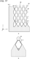
- Fig. 77 is a plan view illustrating an example of a layout of the organic EL film 222 in the second modification of the ninth embodiment of the present technology.
- a circular portion corresponding to a sub-pixel is not disposed in a region near the frame 222-1, but is disposed at a position sufficiently away from the frame 222-1.
- areas of openings 281-3, 281-4, and 281-5 having at least one edge in contact with the frame 222-1 are larger than an area of the opening 282.
- b illustrates an enlarged view of the opening 281-5.
- a minimum value of angles formed by two edges of the opening 281-5 is 60°, which is equivalent to a minimum value of angles formed by two edges of the opening 282. This similarly applies to other openings 281-3 and 281-4. As a result, deterioration of the frame 222-1 can be suppressed.
- the shape of the opening 281-1 having at least one edge in contact with the frame 222-1 is the same as that of the opening 282 having no such an edge, but the present technology is not limited to this layout.
- a display device 100 in a third modification of the ninth embodiment is different from that of the ninth embodiment in that a layout is changed.
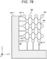
- Fig. 78 is a plan view illustrating an example of a layout of the organic EL film 222 in the third modification of the ninth embodiment of the present technology.
- a boundary of the frame 222-1 has a linear shape, and a circular portion corresponding to a sub-pixel is disposed at a position sufficiently away from the frame 222-1.
- a minimum value of angles formed by two edges is 60°, which is the same as a minimum value of angles formed by two edges of the opening 282.
- a minimum value of angles formed by two edges of the opening 281-7 adjacent to a corner of the frame 222-1 is 90°, which is larger than the angle formed by two edges of the opening 282.
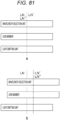
- a relationship among a normal line LN extending through a center of a light emitting unit, a normal line LN' extending through a center of a lens member, and a normal line LN" extending through a center of a wavelength selection unit is described.
- the organic EL film 222 and the like in a sub-pixel correspond to the light emitting unit.
- a size of a wavelength selection unit may be appropriately changed corresponding to light emitted from the light emitting element, or a size of a light absorbing layer (black matrix layer) may be appropriately changed corresponding to light emitted from the light emitting element in a case where the light absorbing layer (black matrix layer) is provided between wavelength selection units (for example, color filter layers) of adjacent light emitting elements.
- the size of the wavelength selection unit (for example, the color filter layer) may be appropriately changed according to a distance (offset amount) d 0 between a normal line passing through a center of the light emitting unit and a normal line passing through a center of a color filter layer CF.
- a planar shape of the wavelength selection unit (for example, the color filter layer) may be the same as, similar to, or different from a planar shape of the lens member.
- a mode may be adopted in which the normal line LN passing through the center of the light emitting unit does not coincide with the normal line LN" passing through the center of the wavelength selection unit and the normal line LN' passing through the center of the lens member, and the normal line LN' passing through the center of the lens member does not coincide with the normal line LN passing through the center of the light emitting unit and the normal line LN" passing through the center of the wavelength selection unit.
- the center of the wavelength selection unit (indicated by a black square in Fig. 80 ) is preferably located on a straight line LL connecting the center of the light emitting unit and the center of the lens member (indicated by a black circle in Fig. 31 ).
- a configuration may be adopted in which the normal line LN passing through the center of the light emitting unit does not coincide with the normal line LN" passing through the center of the wavelength selection unit and the normal line LN' passing through the center of the lens member, and the normal line LN" passing through the center of the wavelength selection unit and the normal line LN' passing through the center of the lens member coincide with each other.
- D 0 d 0 >0 is satisfied.
- a mode may be adopted in which the normal line LN passing through the center of the light emitting unit does not coincide with the normal line LN" passing through the center of the wavelength selection unit and the normal line LN' passing through the center of the lens member, and the normal line LN' passing through the center of the lens member does not coincide with the normal line LN passing through the center of the light emitting unit and the normal line LN" passing through the center of the wavelength selection unit.
- the center of the wavelength selection unit is preferably located on the straight line LL connecting the center of the light emitting unit and the center of the lens member.
- a distance from the center of the light emitting unit to the center of the wavelength selection unit (indicated by a black square in Fig. 82 ) in the thickness direction is LL 1
- a distance from the center of the wavelength selection unit to the center of the lens member (indicated by a black circle in Fig. 82 ) in the thickness direction is LL 2 , d 0 > D 0 > 0
- the pixel used in the display device according to the present disclosure described above may have a resonator structure that causes resonance of light generated in the light emitting unit.
- the resonator structure will be described with reference to the drawings.
- Fig. 83 is a schematic cross-sectional view for explaining a first example of the resonator structure.
- a first electrode 31 is formed to have a common film thickness in each light emitting unit 50. This similarly applies to a second electrode 61.
- a reflector 71 is disposed below the first electrode 31 of the light emitting unit 50 with an optical adjustment layer 72 interposed therebetween.
- the resonator structure that causes resonance of light generated by an organic layer 40 is formed between the reflector 71 and the second electrode 61.
- the reflector 71 is formed to have a common film thickness in each light emitting unit 50.
- the film thickness of the optical adjustment layer 72 is different according to a color to be displayed by the pixel. Since optical adjustment layers 72R, 72G, and 72B have different film thicknesses, it is possible to set an optical distance that causes optimum resonance for a wavelength of light according to the color to be displayed.
- upper surfaces of the reflectors 71 in light emitting units 50R, 50G, and 50B are disposed so as to be aligned.
- positions of upper surfaces of the second electrode 61 are different according to the type of the light emitting units 50R, 50G, and 50B.
- the reflectors 71 can be formed with a metal such as aluminum (Al), silver (Ag), or copper (Cu), or an alloy containing these metals as principal components, for example.
- the optical adjustment layers 72 can be formed with an inorganic insulating material such as silicon nitride (SiNx), silicon oxide (SiOx), or silicon oxynitride (SiOxNy), or an organic resin material such as an acrylic resin or a polyimide resin.
- an inorganic insulating material such as silicon nitride (SiNx), silicon oxide (SiOx), or silicon oxynitride (SiOxNy), or an organic resin material such as an acrylic resin or a polyimide resin.
- SiNx silicon nitride
- SiOxNy silicon oxynitride
- organic resin material such as an acrylic resin or a polyimide resin.
- Each optical adjustment layer 72 may be a single layer, or may be a film stack formed with a plurality of materials. Furthermore, the number of stacked layers may be different according to the type of the light emitting unit 50.
- the first electrode 31 can be formed using a transparent conductive material such as indium tin oxide (ITO), indium zinc oxide (IZO), or zinc oxide (ZnO).
- ITO indium tin oxide
- IZO indium zinc oxide
- ZnO zinc oxide
- the second electrode 61 needs to function as a semi-transmission reflection film.
- the second electrodes 61 can be formed with magnesium (Mg), silver (Ag), a magnesium-silver alloy (MgAg) containing these materials as the principal components, an alloy containing an alkali metal or an alkaline earth metal, or the like.
- b is a schematic cross-sectional view for explaining a second example of the resonator structure.
- the first electrode 31 and the second electrode 61 are formed to have a common film thickness in each light emitting unit 50.
- the reflector 71 is disposed below the first electrode 31 of the light emitting unit 50 with the optical adjustment layer 72 interposed therebetween.
- the resonator structure that causes resonance of light generated by an organic layer 40 is formed between the reflector 71 and the second electrode 61.
- the reflector 71 is formed to have a common film thickness in each light emitting unit 50, and the film thickness of the optical adjustment layer 72 is different according to the color to be displayed by the pixel.
- upper surfaces of the reflectors 71 in the light emitting units 50R, 50G, and 50B have been disposed so as to be aligned, and positions of the upper surfaces of the second electrodes 61 have been different according to the types of the light emitting units 50R, 50G, and 50B.
- the upper surfaces of the second electrodes 61 are disposed so as to be aligned with the light emitting units 50R, 50G, and 50B.
- the upper surfaces of the reflectors 71 in the light emitting units 50R, 50G, and 50B are disposed to be different according to the types of the light emitting units 50R, 50G, and 50B. Therefore, a lower surface (in other words, a surface of a base 73 indicated by reference numeral 73 in the figure) of the reflector 71 has a stair shape according to the type of the light emitting unit 50.
- a is a schematic cross-sectional view for explaining a third example of the resonator structure.
- the first electrode 31 and the second electrode 61 are formed to have a common film thickness in each light emitting unit 50.
- the reflector 71 is disposed below the first electrode 31 of the light emitting unit 50 with the optical adjustment layer 72 interposed therebetween.
- the resonator structure that causes resonance of light generated by the organic layer 40 is formed between the reflector 71 and the second electrode 61.
- the film thickness of the optical adjustment layer 72 is different according to the color to be displayed by the pixel.
- the light emitting units 50R, 50G, and 50B are disposed such that positions of upper surfaces of the second electrodes 61 are aligned.
- the lower surface of the reflector 71 has had a stair shape according to the type of the light emitting unit 50.
- the film thickness of the reflector 71 is set to be different according to the types of the light emitting units 50R, 50G, and 50B. More specifically, the film thickness is set such that lower surfaces of the reflectors 71R, 71G, and 71B are aligned.
- Fig. 84 b is a schematic cross-sectional view for explaining a fourth example of the resonator structure.
- each of the first electrode 31 and the second electrode 61 of each light emitting unit 50 is formed to have a common film thickness. Then, the reflector 71 is disposed below the first electrode 31 of the light emitting unit 50 with the optical adjustment layer 72 interposed therebetween.
- the optical adjustment layer 72 is omitted, and the film thickness of the first electrode 31 is set to be different according to the types of the light emitting units 50R, 50G, and 50B.
- the reflector 71 is formed to have a common film thickness in each light emitting unit 50.
- the film thickness of the first electrode 31 is different according to the color to be displayed by the pixel. Since first electrodes 31R, 31G, and 31B have different film thicknesses, it is possible to set an optical distance that causes optimum resonance for a wavelength of light according to the color to be displayed.
- a is a schematic cross-sectional view for explaining a fifth example of the resonator structure.
- each of the first electrode 31 and the second electrode 61 is formed to have a common film thickness in each light emitting unit 50. Then, the reflector 71 is disposed below the first electrode 31 of the light emitting unit 50 with the optical adjustment layer 72 interposed therebetween.
- the optical adjustment layer 72 has been omitted, and instead, an oxide film 74 has been formed on a surface of the reflector 71.
- a film thickness of the oxide film 74 has been set to be different according to the types of the light emitting units 50R, 50G, and 50B.
- the film thickness of the oxide film 74 is different according to the color to be displayed by the pixel. Since oxide films 74R, 74G, and 74B have different film thicknesses, it is possible to set an optical distance that causes optimum resonance for a wavelength of light according to the color to be displayed.
- the oxide films 74 are films obtained by oxidizing the surfaces of the reflectors 71, and are formed with aluminum oxide, tantalum oxide, titanium oxide, magnesium oxide, zirconium oxide, or the like, for example.
- the oxide films 74 function as insulating films for adjusting the optical path lengths (optical distances) between the reflectors 71 and the second electrodes 61.
- the oxide film 74 having different film thicknesses according to the types of the light emitting units 50R, 50G, and 50B can be formed, for example, as follows.
- an electrolytic solution is filled in the container, and a substrate on which the reflector 71 is formed is immersed in the electrolytic solution. Furthermore, an electrode is disposed so as to face the reflector 71.
- a positive voltage is applied to the reflector 71 with reference to the electrode, and the reflector 71 is anodized.
- a film thickness of the oxide film due to the anodization is proportional to a voltage value for the electrode. Therefore, anodization is performed in a state where a voltage according to the type of the light emitting unit 50 is applied to each of the reflectors 71R, 71G, and 71B. As a result, the oxide films 74 having different film thicknesses can be collectively formed.
- b is a schematic cross-sectional view for explaining a sixth example of the resonator structure.
- the light emitting unit 50 is configured by stacking the first electrode 31, the organic layer 40, and the second electrode 61.
- the first electrode 31 is formed to function as both an electrode and a reflector.
- the first electrode (also serving as a reflector) 31 is formed containing a material having an optical constant selected according to the type of the light emitting units 50R, 50G, and 50B. Since a phase shift by the first electrodes (also serving as reflectors) 31 vary, it is possible to set an optical distance that causes optimum resonance for a wavelength of light according to the color to be displayed.
- the first electrodes (also serving as reflectors) 31 can be formed with a single-component metal such as aluminum (Al), silver (Ag), gold (Au), or copper (Cu), or an alloy containing these metals as the principal components.
- the first electrode (also serving as a reflector) 50R of the light emitting unit 31R may be formed containing copper (Cu)
- the first electrode (also serving as a reflector) 50G of the light emitting unit 31G and the first electrode (also serving as a reflector) 31B of the light emitting unit 50B may be formed containing aluminum.
- Fig. 86 is a schematic cross-sectional view for explaining a seventh example of the resonator structure.
- the sixth example is applied to the light emitting units 50R and 50G, and the first example is applied to the light emitting unit 50B. Also in this configuration, it is possible to set an optical distance that causes optimum resonance for a wavelength of light according to the color to be displayed.
- the first electrodes (also serving as reflectors) 31R and 31G used for the light emitting units 50R and 50G can be formed containing a single metal such as aluminum (Al), silver (Ag), gold (Au), or copper (Cu), or an alloy containing these as a main component.
- the display device can be used as a display unit (display device) of an electronic device in all fields for displaying a video signal input to the electronic device or a video signal generated in the electronic device as an image or a video.
- the display device can be used as a display unit of a television set, a digital still camera, a notebook personal computer, a mobile terminal device such as a mobile phone, a video camera, or a head-mounted display (display to be worn on a head).
- Examples of a display device include a modular display device having a sealed configuration.
- a display module formed by adhering an opposing portion such as transparent glass to the pixel array unit.
- the display module may be provided with a circuit unit for inputting and outputting signals and the like from the outside to the pixel array unit, a flexible printed circuit (FPC) and the like.
- FPC flexible printed circuit
- a digital still camera and a head-mounted display will be exemplified as specific examples of an electronic device using a display device according to the present disclosure.
- the specific example exemplified here is merely an example, and the present technology is not limited thereto.
- a and b illustrate an example of an external appearance of a digital still camera 310.
- the digital still camera 310 is of a lens interchangeable single-lens reflex type, and includes an interchangeable imaging lens unit (interchangeable lens) 312 substantially at the center on the front surface of a camera main body (camera body) 311, and a grip 313 to be held by the photographer on the front left side.
- interchangeable imaging lens unit interchangeable lens
- a monitor 314 is provided at a position shifted to the left side from the center of the rear surface of the camera main body 311.
- An electronic viewfinder (eyepiece window) 315 is provided above the monitor 314. By looking through the electronic viewfinder 315, the photographer can visually recognize an optical image of the subject guided from the imaging lens unit 312, and determine a picture composition.
- the display device 100 according to one of the above-described embodiment and modifications thereof can be used.
- Fig. 88 illustrates an example of an external appearance of a head-mounted display 320.
- the head-mounted display 320 includes ear hooking portions 322 to be worn on the head of the user on both sides of a display unit 321 in the shape of eyeglasses, for example.
- a display unit 321 in the shape of eyeglasses, for example.
- any display device 100 according to one of the above-described embodiment and modifications thereof can be used.
- Fig. 89 illustrates an example of an external appearance of a television device 330.
- the television device 330 includes, for example, a video display screen unit 331 including a front panel 332 and a filter glass 333, and the video display screen unit 331 includes the display device 100 according to one of the above-described embodiment and modifications thereof.
- Fig. 90 is an external view of a see-through head-mounted display.
- a see-through head-mounted display 400 includes a main body 401, an arm 402, and a lens barrel 403.
- the main body 401 is connected to the arm 402 and eyeglasses 410. Specifically, an end portion of the main body 401 in the long side direction is coupled to the arm 402, and one side of a side surface of the main body 401 is coupled to the eyeglasses 410 via a connecting member. Note that the main body 401 may be directly mounted on the head of the human body.
- the main body 401 incorporates a control board for controlling operation of the see-through head-mounted display 400, and a display unit.
- the arm 402 connects the main body 401 and the lens barrel 403, and supports the lens barrel 403. Specifically, the arm 402 is coupled to an end portion of the main body 401 and an end portion of the lens barrel 403, and secures the lens barrel 403. Furthermore, the arm 402 incorporates a signal line for communicating data related to an image to be provided from the main body 401 to the lens barrel 403.
- the lens barrel 403 projects image light provided from the main body 401 via the arm 402 toward the eyes of the user wearing the see-through head-mounted display 400 through an eyeglass.
- a display device according to the present disclosure can be used for the display unit of the main body 401.
- the display device 100 according to the present embodiment can be applied to a display unit included in an electronic device such as a smartphone.
- a smartphone 600 includes a display unit 602 that displays various kinds of information, an operating unit that includes buttons and the like for receiving an operating input by the user, and the like.
- the display unit 602 described above can be the display device 100 according to the present embodiment.
- a and b are views illustrating an internal configuration of a vehicle which is a first application example of an electronic device including the display device 100 according to the present disclosure.
- a is a view illustrating an internal state of the vehicle from a rear side to a front side of the vehicle
- b of Fig. 92 is a view illustrating an internal state of the vehicle from an oblique rear side to an oblique front side of the vehicle.
- the vehicle in a and b of Fig. 92 includes a center display 501, a console display 502, a head-up display 503, a digital rearview mirror 504, a steering wheel display 505, and a rear entertainment display 506.
- the center display 501 is disposed on a dashboard at a location facing a driver's seat 508 and a passenger seat 509.
- Fig. 92 illustrates an example of the center display 501 having a horizontally long shape extending from the driver's seat 508 side to the passenger seat 509 side, but any screen size and arrangement location of the center display 501 may be adopted.
- the center display 501 can display information sensed by various sensors. As a specific example, the center display 501 can display a captured image captured by an image sensor, an image of a distance to an obstacle in front of or on a side of the vehicle, the distance being measured by a ToF sensor, a passenger's body temperature detected by an infrared sensor, and the like.
- the center display 501 can be used to display, for example, at least one of safety-related information, operation-related information, a life log, health-related information, authentication/identification-related information, or entertainment-related information.
- the safety-related information is information about doze sensing, looking-away sensing, sensing of mischief of a child riding together, presence or absence of wearing of a seat belt, sensing of leaving of an occupant, and the like, and is information sensed by a sensor disposed to overlap with the back surface side of the center display 501, for example.
- the operation-related information senses a gesture related to an operation performed by an occupant, using a sensor.
- Gestures to be sensed may include an operation of various kinds of equipment in a vehicle 500. For example, operations of air conditioning equipment, a navigation device, an audiovisual (AV) device, an illuminating device, and the like are detected.
- the lifelogs include lifelogs of all the occupants.
- the life log includes an action record of each occupant in the vehicle.
- the health-related information senses the body temperature of an occupant, using a sensor such as a temperature sensor, and estimates the health condition of the occupant on the basis of the sensed body temperature.
- the face of the occupant may be imaged with an image sensor, and the health condition of the occupant may be estimated from the imaged facial expression.
- a conversation may be made with an occupant in automatic voice, and the health condition of the occupant may be estimated on the basis of the contents of a response from the occupant.
- the authentication/identification-related information includes a keyless entry function of performing face authentication using a sensor, and a function of automatically adjusting a seat height and position through face identification.
- the entertainment-related information includes a function of detecting, with a sensor, operation information about an AV device being used by an occupant, and a function of recognizing the face of the occupant with sensor and providing content suitable for the occupant through the AV device.
- the console display 502 can be used, for example, to display the life log information.
- the console display 502 is disposed near a shift lever 511 of a center console 510 between the driver's seat 508 and the passenger seat 509.
- the console display 502 can also display information detected by various sensors.
- the console display 502 may display an image of the surroundings of the vehicle captured with an image sensor, or may display an image of the distance to an obstacle present in the surroundings of the vehicle.
- the head-up display 503 is virtually displayed behind a windshield 512 in front of the driver's seat 508.
- the head-up display 503 can be used to display, for example, at least one of the safety-related information, the operation-related information, the life log, the health-related information, the authentication/identification-related information, or the entertainment-related information. Being virtually disposed in front of the driver's seat 508 in many cases, the head-up display 503 is suitable for displaying information directly related to operations of the vehicle 500, such as the speed, the remaining amount of fuel (battery), and the like of the vehicle 500.
- the digital rearview mirror 504 can not only display the rear of the vehicle but also display the state of an occupant in the rear seat, and thus, can be used to display the lifelog information by disposing a sensor on the back surface side of the digital rearview mirror 504 in an overlapping manner, for example.
- the steering wheel display 505 is disposed near the center of a steering wheel 513 of the vehicle.
- the steering wheel display 505 can be used to display, for example, at least one of the safety-related information, the operation-related information, the life log, the health-related information, the authentication/identification-related information, or the entertainment-related information.
- the steering wheel display 505 is suitable for displaying the lifelog information such as the body temperature of the driver, or for displaying information regarding operations of the AV device, the air conditioning equipment, or the like.
- the rear entertainment display 506 is attached to the back side of the driver's seat 508 or the passenger seat 509, and is for an occupant in the rear seat to enjoy viewing/listening.
- the rear entertainment display 506 can be used to display, for example, at least one of the safety-related information, the operation-related information, the life log, the health-related information, the authentication/identification-related information, or the entertainment-related information.
- information related to the occupant in the rear seat is displayed as the rear entertainment display 506 is located in front of an occupant in the rear seat. For example, information regarding an operation of the AV device or the air conditioning equipment may be displayed, or a result of measurement of the body temperature or the like of an occupant in the rear seat with a temperature sensor may be displayed.
- Optical distance measurement methods are roughly classified into a passive type and an active type.
- a method of the passive type distance measurement is performed by receiving light from an object, without projecting light from a sensor to the object.
- Methods of the passive type include a lens focus method, a stereo method, and a monocular vision method.
- Methods of the active type include distance measurement that is performed by projecting light onto an object, and receiving reflected light from the object with a sensor to measure the distance.
- Methods of the active type include an optical radar method, an active stereo method, an illuminance difference stereo method, a moire topography method, and an interference method.
- the display device 100 according to the present disclosure can be used in distance measurement by any of these methods. With a sensor disposed on the back surface side of the display device 100 according to the present disclosure in an overlapping manner, distance measurement of the passive type or the active type described above can be performed.
Landscapes
- Physics & Mathematics (AREA)
- Engineering & Computer Science (AREA)
- Microelectronics & Electronic Packaging (AREA)
- Geometry (AREA)
- Optics & Photonics (AREA)
- Electroluminescent Light Sources (AREA)
Abstract
Description
- The present technology relates to a display device. Specifically, the present technology relates to a display device using a light emitting element.
- Conventionally, organic electro luminescence (EL) has been used in display devices and the like in order to reduce backlight and improve image quality. For example, there has been proposed a display device having a structure in which a first electrode is disposed for every sub-pixel, an organic EL film and a second electrode are stacked on the first electrode, and the organic EL film and the second electrode are connected in all sub-pixels in a display region and outside the display region (see, for example, Patent Document 1).
- Patent Document 1:
Japanese Patent Application Laid-Open No. 2014-232568 - In the above-described related art, the organic EL film is connected inside and outside the display region to prevent cracking and peeling of the organic EL film in a patterning process. However, in the above-described related art, it is difficult to suppress a leakage current through the organic EL film.
- The present technology has been made in view of such a situation, and an object thereof is to suppress a leakage current in a display device provided with an organic EL film.
- The present technology has been made to solve the above-described problem, and a first aspect thereof is a display device including: a first electrode and a second electrode having different polarities; and an organic EL film formed between the first electrode and the second electrode when viewed from a direction that is parallel to a predetermined plane, the organic EL film being formed in a predetermined number of sub-pixels and a connection portion that is a portion mutually connecting adjacent sub-pixels in an inter-pixel region between the above-described predetermined number of sub-pixels, when viewed from a vertical direction that is vertical to the above-described predetermined plane. This configuration brings about an effect of suppressing the occurrence of leakage current.
- Furthermore, in the first aspect, the above-described connection portion may be a part of the above-described inter-pixel region. This configuration brings about an effect of suppressing the occurrence of leakage current.
- Furthermore, in the first aspect, the above-described first electrode may be formed for every sub-pixel among the above-described sub-pixels in a predetermined region surrounding the sub-pixel when viewed from the above-described vertical direction, and the above-described second electrode may be formed in the above-described predetermined number of sub-pixels and in the connection portion when viewed from the above-described vertical direction. This configuration brings about an effect that the sub-pixels are individually driven.
- Furthermore, in the first aspect, there may be further provided a protective film covering a pixel array unit in which the above-described predetermined number of sub-pixels are arranged, in which a film thickness of a predetermined portion of the above-described protective film covering the above-described predetermined number of sub-pixels may be larger than a film thickness of a portion that is not considered as the above-described predetermined portion. This configuration brings about an effect of improving light extraction efficiency.
- Furthermore, in the first aspect, the above-described connection portion may be formed in a portion that is not considered as a rectangular region in the above-described inter-pixel region. This configuration brings about an effect of suppressing the occurrence of leakage current.
- Furthermore, in the first aspect, the above-described predetermined number of sub-pixels may be arranged in the pixel array unit, and a width of the above-described second electrode may be a value according to a distance from a central portion of the above-described pixel array unit. This configuration brings about an effect of suppressing shading.
- Furthermore, in the first aspect, one end of the above-described connection portion may be connected to one of a pair of adjacent sub-pixels among the above-described predetermined number of sub-pixels, another end of the above-described connection portion may be connected to another one of the above-described pair of sub-pixels, and a width of the above-described one end may be different from a width of the above-described another end. This configuration brings about an effect that principal ray control is performed.
- Furthermore, in the first aspect, the above-described predetermined number of sub-pixels may be arranged in the pixel array unit, and the above-described width may be a value according to a distance from a center of the above-described pixel array unit. This configuration brings about an effect that principal ray control is performed.
- Furthermore, in the first aspect, the above-described connection portion may include first and second connection portions having a rectangular shape, and a pair of adjacent sub-pixels among the above-described predetermined number of sub-pixels may be connected by the above-described first and second connection portions. This configuration brings about an effect of preventing a connection failure.
- Furthermore, in the first aspect, an edge of the above-described connection portion may have an arc shape. This configuration brings about an effect of preventing a connection failure.
- Furthermore, in the first aspect, a width of a center of the above-described connection portion may be wider than widths of both ends of the above-described connection portion. This configuration brings about an effect of improving light extraction efficiency.
- Furthermore, in the first aspect, an opened region in which the above-described organic EL film is not formed may be provided in a central portion of the above-described connection portion. This configuration brings about an effect of improving light extraction efficiency.
- Furthermore, in the first aspect, the above-described organic EL film may be formed in the above-described predetermined number of sub-pixels, in the above-described connection portion, and in a bridge region mutually connecting the above-described connection portions in the above-described inter-pixel region when viewed from the above-described vertical direction. This configuration brings about an effect of suppressing an increase in resistance of a cathode electrode.
- Furthermore, in the first aspect, a shape of each of the above-described sub-pixels may be a figure in which a core portion and a plurality of protrusions are combined when viewed from the above-described vertical direction. This configuration brings about an effect of improving light extraction efficiency.
- Furthermore, in the first aspect, a shape of the above-described organic EL film as viewed from the above-described vertical direction may be a shape having a predetermined number of bent portions. This configuration brings about an effect of improving light extraction efficiency.
- Furthermore, in the first aspect, unevenness may be formed on a side wall of each of the above-described sub-pixels when viewed from a direction that is parallel to the above-described predetermined plane. This configuration brings about an effect of improving light extraction efficiency.
- Furthermore, in the first aspect, the above-described predetermined number of sub-pixels may be arranged in a delta array. This configuration brings about an effect of suppressing a leakage current in a delta-array display device.
- Furthermore, in the first aspect, the above-described predetermined number of sub-pixels may be arranged in a square array. This configuration brings about an effect of suppressing a leakage current in a square-array display device.
- Furthermore, in the first aspect, the above-described predetermined number of sub-pixels may be arranged in a stripe array. This configuration brings about an effect of suppressing a leakage current in a stripe-array display device.
- Furthermore, in the first aspect, the above-described organic EL film is formed in a frame surrounding a predetermined number of the above-described sub-pixels, in a predetermined number of the above-described sub-pixels, and in the above-described connection portion when viewed from the above-described vertical direction, a plurality of openings is formed in the above-described organic EL film when viewed from the above-described vertical direction, the above-described plurality of openings includes a first opening having at least one edge in contact with the above-described frame and a second opening that is not considered as the above-described first opening, and a smallest angle among angles formed by two edges of the above-described first opening may not exceed a smallest angle among angles formed by two edges of the above-described second opening. This configuration brings about an effect of suppressing deterioration of the frame and pixels around the frame.
-
-
Fig. 1 is a block diagram illustrating a configuration example of a display device according to a first embodiment of the present technology. -
Fig. 2 is an example of a plan view and a cross-sectional view of a pixel array unit according to the first embodiment of the present technology. -
Fig. 3 is an example of a plan view of the pixel array unit and a cross-sectional view taken along a line segment including a connection portion according to the first embodiment of the present technology. -
Fig. 4 is an example of a plan view and a cross-sectional view of a pixel array unit in a comparative example. -
Fig. 5 is a diagram for explaining a manufacturing process up to photolithography according to the first embodiment of the present technology. -
Fig. 6 is a view for explaining a manufacturing process up to film formation of a protective film according to the first embodiment of the present technology. -
Fig. 7 is an example of a delta-array pixel array unit in which sub-pixels arranged in an oblique direction are mutually connected according to the first embodiment of the present technology. -
Fig. 8 is an example of a delta-array pixel array unit in which sub-pixels arranged in a horizontal direction are mutually connected according to the first embodiment of the present technology. -
Fig. 9 is an example of a delta-array pixel array unit in which sub-pixels arranged in a vertical direction are mutually connected according to the first embodiment of the present technology. -
Fig. 10 is an example of a delta-array pixel array unit in which sub-pixels arranged in a horizontal direction, a vertical direction, and an oblique direction are mutually connected according to the first embodiment of the present technology. -
Fig. 11 is an example of a delta-array pixel array unit in which sub-pixels arranged in a horizontal direction and a vertical direction are mutually connected according to the first embodiment of the present technology. -
Fig. 12 is an example of a square-array pixel array unit in which sub-pixels arranged in an oblique direction are mutually connected according to the first embodiment of the present technology. -
Fig. 13 is an example of a square-array pixel array unit in which sub-pixels arranged in a vertical direction are mutually connected according to the first embodiment of the present technology. -
Fig. 14 is an example of a square-array pixel array unit in which sub-pixels arranged in a horizontal direction are mutually connected according to the first embodiment of the present technology. -
Fig. 15 is an example of a square-array pixel array unit in which sub-pixels arranged in a horizontal direction and a vertical direction are mutually connected according to the first embodiment of the present technology. -
Fig. 16 is an example of a square-array pixel array unit in which sub-pixels arranged in a horizontal direction, a vertical direction, and an oblique direction are mutually connected according to the first embodiment of the present technology. -
Fig. 17 is an example of a stripe-array pixel array unit in which sub-pixels arranged in a vertical direction are mutually connected according to the first embodiment of the present technology. -
Fig. 18 is an example of a stripe-array pixel array unit in which sub-pixels arranged in a horizontal direction are mutually connected according to the first embodiment of the present technology. -
Fig. 19 is an example of a stripe-array pixel array unit in which sub-pixels arranged in a vertical direction are mutually connected and connection portions arranged in a horizontal direction are mutually connected, according to the first embodiment of the present technology. -
Fig. 20 is an example of a stripe-array pixel array unit in which sub-pixels arranged in a horizontal direction and a vertical direction are mutually connected according to the first embodiment of the present technology. -
Fig. 21 is an example of a stripe-array pixel array unit in which sub-pixels arranged in a horizontal direction and a vertical direction are mutually connected and connection portions arranged in a horizontal direction are mutually connected, according to the first embodiment of the present technology. -
Fig. 22 is an example of a plan view of a pixel array unit in which a connection portion is formed in a portion other than a rectangular portion, according to the first embodiment of the present technology. -
Fig. 23 is an example of a plan view of a pixel array unit according to a second embodiment of the present technology. -
Fig. 24 is an example of a plan view of a delta-array pixel array unit according to a third embodiment of the present technology. -
Fig. 25 is an example of a plan view of a pixel array unit in which a width is changed according to a distance from a central portion in a delta array according to the third embodiment of the present technology. -
Fig. 26 is an example of a plan view of a square-array pixel array unit according to the third embodiment of the present technology. -
Fig. 27 is an example of a plan view of a pixel array unit in which a width is changed according to a distance from a central portion in a square array according to the third embodiment of the present technology. -
Fig. 28 is an example of a plan view of a pixel array unit in which a connection portion is formed in a T shape according to the third embodiment of the present technology. -
Fig. 29 is an example of a plan view of a pixel array unit according to a fourth embodiment of the present technology. -
Fig. 30 is an example of a plan view of a pixel array unit in a modification of the fourth embodiment of the present technology. -
Fig. 31 is another example of a plan view of a pixel array unit in a modification of the fourth embodiment of the present technology. -
Fig. 32 is an example of a plan view of a pixel array unit according to a fifth embodiment of the present technology. -
Fig. 33 is an example of a plan view of a pixel array unit in a first modification of the fifth embodiment of the present technology. -
Fig. 34 is an example of a cross-sectional view of a pixel array unit taken along a line segment including a connection portion in the first modification of the fifth embodiment of the present technology. -
Fig. 35 is an example of a plan view of a pixel array unit in a second modification of the fifth embodiment of the present technology. -
Fig. 36 is an example of a cross-sectional view of the pixel array unit in the second modification of the fifth embodiment of the present technology. -
Fig. 37 is an example of a plan view of a pixel array unit according to a sixth embodiment of the present technology. -
Fig. 38 is an example of a cross-sectional view of the pixel array unit according to the sixth embodiment of the present technology. -
Fig. 39 is an example of a cross-sectional view taken along a line segment including a connection portion according to the sixth embodiment of the present technology. -
Fig. 40 is a view for explaining a manufacturing process of a display device according to the sixth embodiment of the present technology. -
Fig. 41 is a diagram illustrating an example of a shape of a sub-pixel having four protrusions according to the sixth embodiment of the present technology. -
Fig. 42 is a diagram illustrating an example of a shape of a sub-pixel having five protrusions according to the sixth embodiment of the present technology. -
Fig. 43 is a diagram illustrating an example of a shape of a sub-pixel having six protrusions according to the sixth embodiment of the present technology. -
Fig. 44 is a diagram illustrating an example of a shape of a sub-pixel having eight protrusions according to the sixth embodiment of the present technology. -
Fig. 45 is a diagram illustrating an example of a pixel array unit in which sub-pixels each having four or five protrusions are arranged in a stripe array according to the sixth embodiment of the present technology. -
Fig. 46 is a diagram illustrating an example of a pixel array unit in which sub-pixels each having six or eight protrusions are arranged in a stripe array according to the sixth embodiment of the present technology. -
Fig. 47 is a diagram illustrating an example of a pixel array unit in which sub-pixels each having four or five protrusions are arranged in a delta array according to the sixth embodiment of the present technology. -
Fig. 48 is a diagram illustrating an example of a pixel array unit in which sub-pixels each having six or eight protrusions are arranged in a delta array according to the sixth embodiment of the present technology. -
Fig. 49 is a diagram illustrating an example of a pixel array unit in which sub-pixels each having four or five protrusions are arranged in a square array according to the sixth embodiment of the present technology. -
Fig. 50 is a diagram illustrating an example of a pixel array unit in which sub-pixels each having six or eight protrusions are arranged in a square array according to the sixth embodiment of the present technology. -
Fig. 51 is a plan view of an organic EL film and a cross-sectional view of a pixel array unit according to a seventh embodiment of the present technology. -
Fig. 52 is a diagram for explaining a manufacturing process up to photolithography according to the seventh embodiment of the present technology. -
Fig. 53 is a diagram for explaining a manufacturing process up to film formation of a low refractive index film according to the seventh embodiment of the present technology. -
Fig. 54 is a diagram illustrating an example of a plan view of the organic EL film according to the seventh embodiment of the present technology. -
Fig. 55 is a diagram illustrating another example of a plan view of the organic EL film according to the seventh embodiment of the present technology. -
Fig. 56 is a diagram illustrating an example of a cross-sectional view of the pixel array unit according to the seventh embodiment of the present technology. -
Fig. 57 is a diagram illustrating an example of a plan view of a pixel array unit in which sub-pixels are arranged in a stripe array according to the seventh embodiment of the present technology. -
Fig. 58 is a diagram illustrating an example of a plan view of a pixel array unit in which sub-pixels are arranged in a delta array according to the seventh embodiment of the present technology. -
Fig. 59 is a diagram illustrating an example of a plan view of a pixel array unit in which sub-pixels are arranged in a square array according to the seventh embodiment of the present technology. -
Fig. 60 is a diagram illustrating another example of a plan view of a pixel array unit in which sub-pixels are arranged in a square array according to the seventh embodiment of the present technology. -
Fig. 61 is a diagram illustrating an example of a cross-sectional view of a pixel array unit according to an eighth embodiment of the present technology. -
Fig. 62 is a diagram for explaining a manufacturing process according to the eighth embodiment of the present technology. -
Fig. 63 is a diagram illustrating an example of an arrangement method for sub-pixels according to the eighth embodiment of the present technology. -
Fig. 64 is a diagram illustrating an example of an arrangement method for sub-pixels when a cathode contact electrode is disposed, according to the eighth embodiment of the present technology. -
Fig. 65 is a diagram illustrating an example of a cross-sectional view of a pixel array unit in a first modification of the eighth embodiment of the present technology. -
Fig. 66 is a diagram for explaining a manufacturing process up to formation of a low refractive index film in the first modification of the eighth embodiment of the present technology. -
Fig. 67 is a diagram for explaining a manufacturing process up to formation of a texture film in the first modification of the eighth embodiment of the present technology. -
Fig. 68 is a diagram illustrating an example of a cross-sectional view of a pixel array unit in a second modification of the eighth embodiment of the present technology. -
Fig. 69 is a diagram for explaining a manufacturing process in the second modification of the eighth embodiment of the present technology. -
Fig. 70 is a diagram illustrating an example of a cross-sectional view of a pixel array unit in which a position of unevenness is changed in the second modification of the eighth embodiment of the present technology. -
Fig. 71 is a diagram illustrating an example of a cross-sectional view of a pixel array unit in a third modification of the eighth embodiment of the present technology. -
Fig. 72 is a diagram illustrating an example of a cross-sectional view of a pixel array unit in a fourth modification of the eighth embodiment of the present technology. -
Fig. 73 is a plan view illustrating an example of a layout of an organic EL film according to the first embodiment of the present technology. -
Fig. 74 is an example of a perspective view of an opening according to the first embodiment of the present technology. -
Fig. 75 is a plan view illustrating an example of a layout of the organic EL film according to a ninth embodiment of the present technology. -
Fig. 76 is a plan view illustrating an example of a layout of the organic EL film in a first modification of the ninth embodiment of the present technology. -
Fig. 77 is a plan view illustrating an example of a layout of the organic EL film in a second modification of the ninth embodiment of the present technology. -
Fig. 78 is a plan view illustrating an example of a layout of the organic EL film in a third modification of the ninth embodiment of the present technology. -
Fig. 79 is a conceptual diagram for explaining a relationship among a normal line LN passing through a center of a light emitting unit, a normal line LN' passing through a center of a lens member, and a normal line LN" passing through a center of a wavelength selection unit. -
Fig. 80 is a conceptual diagram for explaining a relationship among the normal line LN passing through a center of the light emitting unit, the normal line LN' passing through a center of the lens member, and the normal line LN" passing through a center of the wavelength selection unit. -
Fig. 81 is a conceptual diagram for explaining a relationship among the normal line LN passing through a center of the light emitting unit, the normal line LN' passing through a center of the lens member, and the normal line LN" passing through a center of the wavelength selection unit. -
Fig. 82 is a conceptual diagram for explaining a relationship among the normal line LN passing through a center of the light emitting unit, the normal line LN' passing through a center of the lens member, and the normal line LN" passing through a center of the wavelength selection unit. -
Fig. 83 is a schematic cross-sectional view for explaining a first example and a second example of a resonator structure. -
Fig. 84 is a schematic cross-sectional view for explaining a third example and a fourth example of the resonator structure. -
Fig. 85 is a schematic cross-sectional view for explaining a fifth example and a sixth example of the resonator structure. -
Fig. 86 is a schematic cross-sectional view for explaining a seventh example of the resonator structure. -
Fig. 87 is a front view and a rear view illustrating an example of an external appearance of a digital still camera. -
Fig. 88 is a perspective view of an example of an external appearance of a head-mounted display. -
Fig. 89 is a perspective view illustrating an example of an external appearance of a television device. -
Fig. 90 is an external view of a see-through head-mounted display. -
Fig. 91 is an external view illustrating an example of an electronic device to which a display unit according to an embodiment of the present disclosure can be applied. -
Fig. 92 is a view illustrating an internal state of a vehicle from a rear side to a front side of the vehicle, and a view illustrating an internal state of the vehicle from an oblique rear side to an oblique front side of the vehicle. - Hereinafter, modes for carrying out the present technology (hereinafter referred to as embodiments) will be described. The description will be given in the following order.
- 1. First embodiment (example in which organic EL film is left at connection portion)
- 2. Second embodiment (example in which organic EL film is left at connection portion and width of cathode electrode is adjusted)
- 3. Third Embodiment (example in which organic EL film is left at connection portion and width of connection portion is adjusted)
- 4. Fourth embodiment (example in which organic EL film is left at connection portion and connection portion is increased)
- 5. Fifth embodiment (example in which organic EL film is left at connection portion and width of center of connection portion is increased)
- 6. Sixth embodiment (example in which organic EL film is left at connection portion and shape of sub-pixel is changed)
- 7. Seventh embodiment (example in which organic EL film is left at connection portion and organic EL film is bent in sub-pixel)
- 8. Eighth embodiment (example in which organic EL film is left at connection portion and unevenness is formed on side wall of sub-pixel)
- 9. Ninth embodiment (example in which organic EL film is left at connection portion and angle of opening of organic EL film is increased)
-
Fig. 1 is a block diagram illustrating a configuration example of adisplay device 100 according to a first embodiment of the present technology. Thedisplay device 100 includes acontrol circuit 111, anH driver 112, aV driver 113, and apixel array unit 120. As thedisplay device 100, a display integrated with an electronic device such as a smartphone or a personal computer, a monitor device separated from the electronic device, or the like is assumed. - In the
pixel array unit 120, a plurality ofpixels 200 is arranged. Each of thepixels 200 includes a plurality of sub-pixels that emits light beams of mutually different colors. For example, sub-pixels 201, 202, and 203 that emit R, G, and B light beams are disposed for everypixel 200. Each shape of the sub-pixels 201, 202, and 203 is a hexagonal shape, and these three are arranged in a triangular shape, for example. That is, the sub-pixels are arranged in a delta array. Note that a shape and an arrangement of the sub-pixels are not limited to the hexagonal shape and the delta array. - The
control circuit 111 controls a drive timing of each of theH driver 112 and theV driver 113 on the basis of image data. TheH driver 112 drives the sub-pixels on a column basis. TheV driver 113 drives the sub-pixels on a row basis. -
Fig. 2 is an example of a plan view and a cross-sectional view of thepixel array unit 120 according to the first embodiment of the present technology. In the figure, a is an example of a plan view of thepixel array unit 120, and b in the figure is an example of a cross-sectional view of thepixel array unit 120. - The plurality of sub-pixels such as the sub-pixel 201 is arranged on a predetermined plane. Hereinafter, an axis perpendicular to the plane is referred to as a "Z axis", and a predetermined axis parallel to the plane will be assumed as an "X axis". An axis perpendicular to the X axis and the Z axis will be assumed as a "Y axis". Furthermore, the X-axis direction can also be referred to as a "horizontal direction". The Y-axis direction can also be referred to as a "vertical direction".
- As described above, each of the sub-pixels has, for example, a hexagonal shape. A region surrounded by a one-dotted chain line in a of the figure indicates the sub-pixel 201. Furthermore, the plurality of sub-pixels is arranged at regular intervals. A region between the sub-pixels is hereinafter referred to as an "inter-pixel region". In a of the figure, a region including a hatched portion and a white portion corresponds to the inter-pixel region.
- In the figure, b illustrates a cross-sectional view of the
pixel array unit 120 taken along a line segment between coordinates (X3, Y4) and (X8, Y4) in a of the figure. Thepixel array unit 120 includes asubstrate 240,protective films cathode electrode 221, anorganic EL film 222, a plurality ofanode electrodes 223, and an insulatingfilm 230. - On a substrate plane of the
substrate 240, theanode electrode 223 is formed for every sub-pixel. Hereinafter, a direction from thesubstrate 240 to theanode electrode 223 is referred to as an "upper" direction. Theindividual anode electrodes 223 are separated (in other words, insulated) from each other by the insulatingfilm 230 formed between theanode electrodes 223. The hatched portion corresponds to theanode electrode 223, and the white portion corresponds to the insulatingfilm 230. - The
organic EL film 222 is formed above theanode electrode 223, and thecathode electrode 221 is formed above the organic EL film. Furthermore, theprotective film 212 is formed above thecathode electrode 221, and theprotective film 211 covering theprotective film 212 and a portion between the pixels is formed above theprotective film 212 and the portion between the pixels. Although theprotective films protective films protective film 210. - Since the
protective film 212 is formed above the sub-pixel, a film thickness of a portion of theprotective film 210 covering the sub-pixel is larger than a film thickness of other portion. In other words, theprotective film 210 is raised at the portion of the sub-pixel. Furthermore, on the top and a side surface of theprotective film 210, a low refractive index film (not illustrated) is filled. Therefore, light emitted from the sub-pixel is reflected upward by the side surface (in other words, a surface of the protective film) of the raised portion. A thick arrow in a of the figure indicates an optical path of light emitted by the sub-pixel. - Furthermore, in a of the figure, the
protective films cathode electrode 221 are omitted in order to clearly illustrate a planar shape of theorganic EL film 222. A gray portion in a of the figure indicates theorganic EL film 222. As exemplified in a of the figure, theorganic EL film 222 is formed in each of the plurality of sub-pixels and in a portion mutually connecting adjacent sub-pixels in the inter-pixel region. In the inter-pixel region, a portion where theorganic EL film 222 is formed is hereinafter referred to as a "connection portion". A rectangular portion of a dotted line surrounded by coordinates (X2, Y1), (X6, Y1), (X2, Y3), and (X6, Y3) in a of the figure corresponds to the connection portion. - Furthermore, the
anode electrode 223 is formed in a predetermined region surrounding the sub-pixel when viewed from the Z-axis direction. An outer periphery (coordinate X5, and the like) of a hatched portion in a of the figure corresponds to an outer periphery of theanode electrode 223. Furthermore, a planar shape of thecathode electrode 221 is similar to that of theorganic EL film 222. Furthermore, an end portion of the insulatingfilm 230 reaches an end portion of theanode electrode 223, and is raised by a thickness of the electrode. A hexagonal shape of a one-dotted chain line passing through the coordinate X4 and the like indicates an outer periphery of the raised portion of the insulatingfilm 230. In the following figures, the one-dotted chain line is omitted. - Note that the
anode electrode 223 is an example of a first electrode described in the claims, and thecathode electrode 221 is an example of a second electrode described in the claims. -
Fig. 3 is an example of a plan view of thepixel array unit 120 and a cross-sectional view taken along a line segment including the connection portion according to the first embodiment of the present technology. In the figure, a is an example of a plan view of thepixel array unit 120. In the figure, b illustrates a cross-sectional view taken along a line segment between coordinates (X1, Y2) and (X7, Y2) in a of the figure. It is assumed that the line segment includes the connection portion between sub-pixels. As exemplified in b of the figure, theorganic EL film 222 and thecathode electrode 221 are also formed in the connection portion, and adjacent sub-pixels are mutually connected by theorganic EL film 222 and thecathode electrode 221. - As exemplified in
Figs. 2 and3 , theorganic EL film 222 is formed in each of the plurality of sub-pixels and a portion (that is, the connection portion) that mutually connects adjacent sub-pixels in the inter-pixel region between the sub-pixels, when viewed from the Z-axis direction. Furthermore, theorganic EL film 222 is formed between thecathode electrode 221 and theanode electrode 223 when viewed from the Y-axis direction or the X-axis direction. Note that thecathode electrode 221 and theanode electrode 223 are examples of a first electrode and a second electrode described in the claims. - Furthermore, the
anode electrode 223 is formed for every sub-pixel in a predetermined region surrounding the sub-pixel when viewed from the Z-axis direction. Similarly to theorganic EL film 222, thecathode electrode 221 is formed in each of the plurality of sub-pixels and in the connection portion when viewed from the Z-axis direction. Furthermore, a film thickness of a portion covering the sub-pixel in the protective film 210 (protective films 211 and 212) is larger than a film thickness of other portion. - Here, a
display device 100 having a structure in which theorganic EL film 222 is formed over the entire inter-pixel region and the protective film is not raised in the portion of the sub-pixel is assumed as a comparative example. -
Fig. 4 is an example of a plan view and a cross-sectional view of apixel array unit 120 in the comparative example. In the figure, a is an example of a plan view of thepixel array unit 120, and b of the figure is an example of a cross-sectional view taken along a line segment between coordinates (X1, Y1) and (X2, Y1) in a of the figure. - As exemplified in the figure, the
organic EL film 222 is formed on each of the sub-pixels and the entire inter-pixel region between the sub-pixels. This similarly applies to thecathode electrode 221. Furthermore, a film thickness of theprotective film 211 is assumed to be substantially the same between a portion above the sub-pixel and a portion above the inter-pixel region. - In the comparative example, since the sub-pixels are mutually connected by the
organic EL film 222, a leakage current flowing through theorganic EL film 222 tends to increase. A dotted arrow in the figure indicates the leakage current. - On the other hand, in the structure in which the
organic EL film 222 is formed in a part (connection portion) of the inter-pixel region as exemplified inFigs. 2 and3 , the leakage current can be made smaller than that in the comparative example in which theorganic EL film 222 is formed in the entire region. Note that, in a configuration in which noorganic EL film 222 is formed over the entire inter-pixel region, theorganic EL film 222 and thecathode electrode 221 on the sub-pixel are isolated, and power cannot be supplied to each of the sub-pixels. In order to prevent this state, inFig. 2 , theorganic EL film 222 is left at the connection portion. - Furthermore, in the comparative example, since the
protective film 211 is not raised above the sub-pixel, light emitted from the sub-pixel may be reflected downward on a surface of the protective film. A thick arrow in the figure indicates an optical path of light reflected by the surface of the protective film. - On the other hand, as exemplified in
Fig. 2 , in the structure in which the protective film is raised above the sub-pixel, light can be reflected upward by a side surface (a surface of the protective film) of the raised portion. As a result, light extraction efficiency can be improved as compared with the comparative example. -
Fig. 5 is a diagram for explaining a manufacturing process up to photolithography according to the first embodiment of the present technology. In the figure, a illustrates a cross-sectional view of thepixel array unit 120 in which theanode electrode 223 and the insulatingfilm 230 are formed. In the figure, b illustrates a cross-sectional view of thepixel array unit 120 in which theorganic EL film 222, thecathode electrode 221, and theprotective film 212 are formed. In the figure, c illustrates a cross-sectional view of thepixel array unit 120 when photolithography is performed. - As exemplified in a of the figure, a manufacturing system forms the
anode electrode 223 for every sub-pixel on thesubstrate 240, and forms the insulatingfilm 230 between theanode electrodes 223. Then, as exemplified in b of the figure, the manufacturing system forms theorganic EL film 222 and thecathode electrode 221, and forms theprotective film 212 on thecathode electrode 221. Subsequently, the manufacturing system disposes aphotoresist 250 on each of the sub-pixels, and performs photolithography. -
Fig. 6 is a diagram for explaining a manufacturing process up to film formation of theprotective film 211 according to the first embodiment of the present technology. In the figure, a illustrates a cross-sectional view of thepixel array unit 120 after photolithography. In the figure, b illustrates a cross-sectional view of thepixel array unit 120 on which theprotective film 211 is formed. - As exemplified in a of the figure, while the
protective film 212 above the sub-pixel is left, theprotective film 212 of other portion is removed by photolithography. Then, as exemplified in b of the figure, the manufacturing system forms theprotective film 211. As a result, thepixel array unit 120 having the structure exemplified inFig. 2 is obtained. - In
Fig. 2 , sub-pixels arranged in an oblique direction and the horizontal direction (X-axis direction) are mutually connected by theorganic EL film 222, but the present technology is not limited to this configuration. - For example, as exemplified in
Fig. 7 , the number of connection portions in the horizontal direction can be reduced, to mutually connect only sub-pixels arranged in the oblique direction. - Alternatively, as exemplified in
Fig. 8 , it is also possible to reduce the number of connection portions in the oblique direction, to mutually connect only sub-pixels arranged in the horizontal direction. - Alternatively, as exemplified in
Fig. 9 , it is also possible to reduce the number of connection portions in the horizontal direction and the oblique direction, provide connection portions in a vertical direction (Y-axis direction), to mutually connect sub-pixels arranged in the vertical direction. - Alternatively, as exemplified in
Fig. 10 , connection portions in the vertical direction may be added, to mutually connect sub-pixels arranged in the horizontal direction, the vertical direction, and the oblique direction. - Alternatively, as exemplified in
Fig. 11 , it is also possible to reduce the number of connection portions in the oblique direction and add the connection portions in the horizontal direction, to mutually connect sub-pixels arranged in the horizontal direction and the vertical direction. - Furthermore, in
Fig. 2 andFigs. 7 to 11 , the sub-pixels are arranged in a delta array, but the present technology is not limited to this configuration. As exemplified inFigs. 12 to 16 , the sub-pixels may have a square shape, and may be arranged in a square array. - At that time, as exemplified in
Fig. 12 , the connection portions may be provided in the oblique direction to mutually connect sub-pixels arranged in the oblique direction. - Alternatively, as exemplified in
Fig. 13 , the connection portions may be provided in the vertical direction to mutually connect sub-pixels arranged in the vertical direction. - Alternatively, as exemplified in
Fig. 14 , the connection portions may be provided in the horizontal direction to mutually connect sub-pixels arranged in the horizontal direction. - Alternatively, as exemplified in
Fig. 15 , the connection portions may be provided in the horizontal direction and the vertical direction, to mutually connect sub-pixels arranged in the horizontal direction and the vertical direction. - Alternatively, as exemplified in
Fig. 16 , the connection portions may be provided in the horizontal direction, the vertical direction, and the oblique direction, to mutually connect sub-pixels arranged in the horizontal direction, the vertical direction, and the oblique direction. - Furthermore, as exemplified in
Figs. 17 to 21 , the sub-pixel may have a rectangular shape, and may be arranged in a stripe array. - At that time, as exemplified in
Fig. 17 , the connection portions may be provided in the vertical direction to mutually connect sub-pixels arranged in the vertical direction. - Alternatively, as exemplified in
Fig. 18 , the connection portions may be provided in the horizontal direction to mutually connect sub-pixels arranged in the horizontal direction. - Alternatively, as exemplified in
Fig. 19 , sub-pixels arranged in the vertical direction may be mutually connected, and further, the connection portions arranged in the horizontal direction may be mutually connected. - Alternatively, as exemplified in
Fig. 20 , the connection portions may be provided in the horizontal direction and the vertical direction, to mutually connect sub-pixels arranged in the horizontal direction and the vertical direction. - Alternatively, as exemplified in
Fig. 21 , sub-pixels arranged in the horizontal direction and the vertical direction may be mutually connected, and the connection portions arranged in the horizontal direction may be mutually connected. - Note that, in the above-described example, the rectangular portion in the inter-pixel region is used as the connection portion, but the present technology is not limited to this configuration. As exemplified in
Fig. 22 , theorganic EL film 222 can also be formed by using, as the connection portion, a portion other than the rectangular portion in the inter-pixel region between the adjacent sub-pixels. In the figure, a Y-shaped portion surrounded by a thick dotted line corresponds to the connection portion. In this case, a part of theanode electrode 223 and a part of the insulatingfilm 230 are disposed in the rectangular portion. - As described above, according to the first embodiment of the present technology, since the
organic EL film 222 is formed in each of the sub-pixels and the connection portion in the inter-pixel region, it is possible to reduce the leakage current as compared with the case where theorganic EL film 222 is formed in the entire inter-pixel region. - Furthermore, since the film thickness of the portion covering the sub-pixel in the
protective film 210 is made larger than the film thickness of the other portion, the light extraction efficiency can be improved. - In the first embodiment described above, a width of each
cathode electrode 221 of the connection portion in thepixel array unit 120 is constant, but it is difficult to suppress shading in this configuration. Adisplay device 100 according to a second embodiment is different from that of the first embodiment in that a width of acathode electrode 221 is changed according to a distance from a central portion. -
Fig. 23 is an example of a plan view of apixel array unit 120 according to the second embodiment of the present technology. Thepixel array unit 120 of the second embodiment is different from that of the first embodiment in that a width of thecathode electrode 221 of a connection portion between sub-pixels is smaller as being closer to a central portion. - Here, when a current flows through the
cathode electrode 221, a potential drop (in other words, IR drop) occurs due to resistance of thecathode electrode 221, and a potential difference between an anode and a cathode in individual pixels decreases. A cathode contact electrode (not illustrated) that supplies a potential to thecathode electrode 221 is disposed in a periphery of thepixel array unit 120. Therefore, as being farther from the periphery, in other words, as being closer to a center of thepixel array unit 120, a potential difference becomes smaller, a current flowing through anorganic EL film 222 decreases, and luminance decreases. As a result, luminance becomes non-uniform, and shading may occur. - By setting the width of the
cathode electrode 221 to be narrower as being closer to the central portion, an area of side-wall reflection exemplified inFig. 2 is increased as being closer to the center, and the light extraction efficiency is improved. Therefore, it is possible to suppress a decrease (that is, shading) in luminance in the central portion. - As described above, according to the second embodiment of the present technology, since the width of the
cathode electrode 221 of the connection portion is set to a value according to a distance from the central portion, shading can be suppressed. - In the first embodiment described above, the width of the connection portion of the
organic EL film 222 is constant. However, in this configuration, it is necessary to shift a position of a lens to change a direction of a principal ray when principal ray control is performed. Adisplay device 100 according to a third embodiment is different from that of the first embodiment in that the principal ray control is realized by setting a width of one end of a connection portion to a value different from that of another end. -
Fig. 24 is an example of a plan view of a delta-arraypixel array unit 120 according to the third embodiment of the present technology. In the third embodiment, a width of one end of a connection portion of anorganic EL film 222 is different from that of another end. For example, a width of one end farther from a central portion of thepixel array unit 120 out of both ends of the connection portion is assumed to be wider than a width of another end. Furthermore, the width gradually changes from one end to another end. - For example, an X coordinate of the central portion of the
pixel array unit 120 is assumed to be X3. On a left side of the coordinate X3, a width of a left end at the coordinate X1 or the like is wider than a width of a right end at the coordinate X2 or the like. On a right side of the coordinate X3, a width of a left end at the coordinate X4 or the like is narrower than a right end at the coordinate X5 or the like. Similarly, on an upper side of the central portion, a width of an upper end of the connection portion is wider than a width of a lower end. On a lower side of the central portion, a width of an upper end of the connection portion is narrower than a width of a lower end. In this way, by setting the width of one end farther from the central portion to be wider than the width of another end for every connection portion, the principal ray can be directed toward the center without shifting a position of a lens. With this principal ray control, light can be collected at the central portion of thedisplay device 100. Note that, in the figure, the connection portion on the upper side and the lower side of the central portion is omitted. - Note that, as exemplified in
Fig. 25 , it is preferable to change the width of the connection portion according to a distance from the central portion. For example, the width of the connection portion may simply be increased as the distance from the central portion increases. An X coordinate of the central portion is assumed to be X5. On a left side of the coordinate X5, a width of a left end at the coordinate X1 of a certain connection portion is wider than a width of a right end at the coordinate X2. A width of a left end at the coordinate X3 of a connection portion closer to the central portion than the certain connection portion is wider than a width of a right end at the coordinate X4, and widths of the coordinates X3 and X4 are narrower respectively than widths of the coordinates X1 and X2. - On a right side of the coordinate X5, a width of a left end at the coordinate X6 of a certain connection portion is narrower than a right end at the coordinate X7. A width of a left end at the coordinate X8 of a connection portion farther from the central portion than the certain connection portion is narrower than a right end at the coordinate X9, and widths at coordinates X8 and X9 are respectively wider than widths at coordinates X6 and X7.
- Similarly, on an upper side of the central portion, the width of the connection portion becomes wider as being closer to an upper end of the
pixel array unit 120. On a lower side of the central portion, the width of the connection portion becomes wider as being closer to a lower end of thepixel array unit 120. - Furthermore, as exemplified in
Fig. 26 , in the square array, a width of one end of the connection portion can be set to a value different from that of another end. - As exemplified in
Fig. 27 , the width of the connection portion can be changed according to a distance from the central portion in the square array. - Furthermore, the width is gradually changed from one end to another end, but the present technology is not limited to this configuration. For example, as exemplified in
Fig. 28 , the connection portion can be formed in a T shape. - As described above, according to the third embodiment of the present technology, since the width of one end of the connection portion is set to a value different from that of another end, the principal ray control can be performed without shifting the position of the lens.
- In the first embodiment described above, adjacent sub-pixels are mutually connected by the connection portion. However, if the connection portion is too thin, the connection portion may be broken and the sub-pixel may be become a black spot due to a connection failure. A
display device 100 according to a fourth embodiment is different from that of the first embodiment in that a connection failure is prevented. -
Fig. 29 is an example of a plan view of apixel array unit 120 according to the fourth embodiment of the present technology. Thepixel array unit 120 of the fourth embodiment is different from that of the first embodiment in that, in a case where attention is paid to a pair of adjacent sub-pixels, the sub-pixels are connected by two connection portions. In the figure, a portion surrounded by a thick dotted line corresponds to the connection portion. - Note that a pair of adjacent sub-pixels can be connected by three or more sub-pixels. By increasing the number of the connection portions to two or more, even if a connection failure occurs in one connection portion, the connection between the sub-pixels can be maintained by the remaining connection portions. As a result, a connection failure can be prevented.
- Note that the two connection portions between the pair of sub-pixels are examples of first and second connection portions described in the claims.
- As described above, according to the fourth embodiment of the present technology, since the pair of adjacent sub-pixels are connected by the two connection portions, connection failure can be prevented.
- In the fourth embodiment described above, the number of connection portions is increased to two or more. However, even with this configuration, connection failure may not be sufficiently prevented. A
display device 100 in a modification of the fourth embodiment is different from that of the fourth embodiment in that an edge of a connection portion has an arc shape. -
Fig. 30 is an example of a plan view of apixel array unit 120 according to the modification of the fourth embodiment of the present technology. Thepixel array unit 120 according to the modification of the fourth embodiment is different from that of the fourth embodiment in that there is one connection portion between a pair of adjacent sub-pixels and an edge of the connection portion has an arc shape. The edge of the connection portion has, for example, an arc shape of a fan. A region surrounded by a thick dotted line in the figure corresponds to the connection portion. By forming the edge of the connection portion in the arc shape, a disconnection failure between the sub-pixels can be reduced. - Note that, as exemplified in
Fig. 31 , a Y-shaped connection portion may be disposed in the vicinity of a vertex of a hexagonal sub-pixel, and an edge of the connection portion may have an arc shape. A region surrounded by a thick dotted line in the figure corresponds to the connection portion. - Furthermore, in the modification of the fourth embodiment, as exemplified in
Fig. 29 , two or more connection portions can be provided between a pair of sub-pixels. - As described above, according to the modification of the fourth embodiment of the present technology, since the edge of the connection portion is formed in the arc shape, connection failure can be prevented.
- In the first embodiment described above, the connection portion has a rectangular shape. However, with this configuration, it is difficult to further improve the light extraction efficiency. A
display device 100 according to a fifth embodiment is different from that of the first embodiment in that a width of a center of a connection portion is increased to improve the light extraction efficiency. -
Fig. 32 is an example of a plan view of apixel array unit 120 according to the fifth embodiment of the present technology. Thepixel array unit 120 of the fifth embodiment is different from that of the first embodiment in that a width of a center of the connection portion is wider than widths of both ends of the connection portion. For example,hexagonal sub-pixels - By increasing the width of the center, it is possible to increase a region reflected at an interface between a
protective film 211 and a low refractive index film, and the light extraction efficiency is improved. Furthermore, by increasing the width of the center of the connection portion, resistance of the connection portion can be reduced, and a voltage rise can be suppressed. - As described above, according to the fifth embodiment of the present technology, since the width of the center of the connection portion is widened, the light extraction efficiency can be improved.
- In the fifth embodiment described above, the width of the center of the connection portion is increased. However, with this configuration, it is difficult to further improve the light extraction efficiency. A
display device 100 in a first modification of the fifth embodiment is different from that of the fifth embodiment in that a central portion of a connection portion is opened. -
Fig. 33 is an example of a plan view of apixel array unit 120 in the first modification of the fifth embodiment of the present technology. The first modification of the fifth embodiment is different from the fifth embodiment in that a part of the central portion of the connection portion of thepixel array unit 120 is opened, and anorganic EL film 222 is not formed in the opened region. In the figure, a thick rectangle between the coordinates X2 and X3 indicates the opened region. -
Fig. 34 is a cross-sectional view taken along a line segment between coordinates (X1, Y2) and (X4, Y2) inFig. 33 . By eliminating theorganic EL film 222 near the center of the connection portion, light from a sub-pixel can be reflected at an interface between theprotective film 211 and a sealing resin above theprotective film 211. As a result, the light extraction efficiency is further improved. An arrow inFig. 34 indicates a trajectory of light reflected by at interface. - As described above, according to the first modification of the fifth embodiment of the present technology, since the central portion of the connection portion is opened, the light extraction efficiency can be further improved.
- In the fifth embodiment described above, the width of the center of the connection portion is increased. However, connection portions may be mutually connected. A
display device 100 in a second modification of the fifth embodiment is different from that of the fifth embodiment in that adjacent connection portions are mutually connected. -
Fig. 35 is an example of a plan view of apixel array unit 120 in the second modification of the fifth embodiment of the present technology. In the second modification of the fifth embodiment, theorganic EL film 222 is also formed in a region extending from a central portion of a connection portion along an edge of a sub-pixel, and adjacent sub-pixels are mutually connected. A region where the sub-pixels are mutually connected is hereinafter referred to as a "bridge portion". A Y-shaped region surrounded by a thick dotted line at the same time indicates the bridge portion. Theorganic EL film 222 is formed in the hexagonal sub-pixel, the connection portion mutually connecting the sub-pixels, and the bridge portion mutually connecting the connection portions. -
Fig. 36 is a cross-sectional view taken along a line segment between coordinates (X1, Y2) and (X2, Y2) inFig. 35 . - As the width of the connection portion is made narrower, resistance of a
cathode electrode 221 above the connection portion becomes larger. However, as exemplified inFigs. 35 and36 , by mutually connecting the connection portions by using the bridge portion, the resistance of thecathode electrode 221 can be reduced by the increased amount. This configuration makes it possible to suppress an increase in resistance of thecathode electrode 221 when the width of the connection portion is narrowed. - As described above, according to the second modification of the fifth embodiment of the present technology, since the
organic EL film 222 is also formed in the bridge portion mutually connecting the connection portions, an increase in the resistance of thecathode electrode 221 can be suppressed. - In the first embodiment described above, the hexagonal sub-pixels are arranged when viewed from the Z-axis direction, but it is difficult to further improve the light extraction efficiency with the shape of the sub-pixels. A
display device 100 according to a sixth embodiment is different from that of the first embodiment in that the light extraction efficiency is improved by providing unevenness on a side wall of a sub-pixel when viewed from the Z-axis direction. -
Fig. 37 is an example of a plan view of apixel array unit 120 according to the sixth embodiment of the present technology. In the figure, a is an example of a plan view when viewed from the Z-axis direction without an on-chip lens 261 and acolor filter 262, and b of the figure is an example of a plan view when three sub-pixels are viewed from the Z-axis direction. - As exemplified in a of the figure, when viewed from the Z-axis direction, unevenness is provided on a side wall for each of the sub-pixels such as a sub-pixel 201. Hereinafter, a portion of the sub-pixel protruding from the side surface is referred to as a "protrusion", and a portion other than the protrusion is referred to as a "core portion". The planar shape of the sub-pixel viewed from the Z-axis direction can be expressed as a figure in which the core portion and the plurality of protrusions are combined. Here, more specifically, the shape of the sub-pixel corresponds to a shape of each of an
organic EL film 222 excluding a connection portion, acathode electrode 221, and aprotective film 211. Furthermore, adjacent sub-pixels are connected to each other by the connection portion in an oblique direction. - A portion surrounded by a thick dotted line in a of the figure corresponds to the core portion. For example, the sub-pixel has a shape (in other words, a cross shape) in which the core portion is rectangular and a rectangular protrusion is adjacent to each of four edges of the core portion.
- Furthermore, as exemplified in b of the figure, the on-
chip lens 261 and thecolor filter 262 are provided in each of the sub-pixels 201 to 203. A circular line indicates an outer periphery of the on-chip lens 261, and a rectangular thick frame indicates an outer periphery of thecolor filter 262. In b of the figure, the connection portion is omitted. -
Fig. 38 is an example of a cross-sectional view of thepixel array unit 120 according to the sixth embodiment of the present technology. This figure is an example of a cross-sectional view taken along a line segment Xa-Xb in the horizontal direction including the core portion in b ofFig. 37 . Furthermore, a thick dotted line inFig. 38 indicates a cross-sectional shape of the protrusion taken along a line segment Xc-Xd including only the protrusion out of the core portion and the protrusion in b ofFig. 37 . Furthermore, an arrow indicates an optical path of light emitted by theorganic EL film 222. By providing unevenness on the side wall, the protrusion functions as a light guide, and the light extraction efficiency can be improved. - Furthermore, in a case where the sub-pixels are connected in the oblique direction, the cross section taken along the line segment Xa-Xb in the horizontal direction does not include the connection portion. Adjacent sub-pixels in this cross section are separated from each other by the insulating
film 230. Furthermore, a lowrefractive index film 270 is formed below thecolor filter 262. -
Fig. 39 is an example of a cross-sectional view taken along a line segment including the connection portion according to the sixth embodiment of the present technology. This figure is an example of a cross-sectional view taken along a line segment Xe-Xf in the oblique direction in a ofFig. 37 . In a case where the sub-pixels are connected in the oblique direction, the cross section taken along the line segment Xe-Xf in the oblique direction includes the connection portion. The adjacent sub-pixels are connected to each other by the connection portion. -
Fig. 40 is a diagram for explaining a manufacturing process of thedisplay device 100 according to the sixth embodiment of the present technology. In the figure, a illustrates a cross-sectional view before photolithography, and b illustrates a cross-sectional view after photolithography. - As exemplified in a of the figure, a manufacturing system forms the
organic EL film 222 and thecathode electrode 221, then forms theprotective film 211 on the organic EL film and the cathode electrode, and disposes aphotoresist 250 on the protective film. A shape of thephotoresist 250 as viewed from the Z-axis direction is a shape obtained by hollowing out the connection portion and the sub-pixel having unevenness. Then, the manufacturing system performs photolithography. As a result, as exemplified in b of the figure, theprotective film 211 is processed into a shape having unevenness. In the figure, b illustrates a cross section taken along the line segment Xa-Xb inFig. 37 . -
Fig. 41 is a diagram illustrating an example of a shape of a sub-pixel having four protrusions according to the sixth embodiment of the present technology. In a case where the core portion has a rectangular shape, up to four protrusions can be provided. In this case, as exemplified in a of the figure, the protrusion may also have a triangular shape. Furthermore, as exemplified in b of the figure, the protrusion may also be formed in a rectangular shape, and the protrusion may also be disposed adjacent to a vertex of the core portion. Note that, as exemplified inFig. 37 , the protrusion may also be formed in a rectangular shape and disposed adjacent to four edges of the core portion. - Furthermore, as exemplified in c of
Fig. 41 , the protrusion may be a semicircle. As exemplified in d of the figure, the protrusion may be a wedge. -
Fig. 42 is a diagram illustrating an example of a shape of a sub-pixel having five protrusions according to the sixth embodiment of the present technology. In a case where the core portion has a pentagonal shape, up to five protrusions can be provided. In this case, as exemplified in a of the figure, the protrusion may also have a triangular shape. Furthermore, as exemplified in b of the figure, the protrusion may have a rectangular shape. -
Fig. 43 is a diagram illustrating an example of a shape of a sub-pixel having six protrusions according to the sixth embodiment of the present technology. In a case where the core portion has a hexagonal shape, up to six protrusions can be provided. In this case, as exemplified in a of the figure, the protrusion may also have a triangular shape. Furthermore, as exemplified in b of the figure, the protrusion may have a rectangular shape. As exemplified in c of the figure, the protrusion may have a hexagonal shape. -
Fig. 44 is a diagram illustrating an example of a shape of a sub-pixel having eight protrusions according to the sixth embodiment of the present technology. In a case where the core portion has an octagonal shape, up to eight protrusions can be provided. In this case, as exemplified in a of the figure, the protrusion may also have a triangular shape. Furthermore, as exemplified in b of the figure, the protrusion may have a rectangular shape. - Theoretically, the number of protrusions can be set to nine or more. However, as the number of protrusions is increased, there is a higher possibility that a resolution limit of lithography is exceeded, and the function of the protrusions as light guides is deteriorated as the shape is closer to a circular shape. For this reason, the cases where the number of protrusions is four to eight, which are highly practical, have been exemplified.
- Although the connection portions are disposed only in the oblique direction, the connection portions may also be disposed in the vertical direction and the horizontal direction as described above.
- Furthermore, as exemplified in
Figs. 45 and46 , sub-pixels can be arranged in a stripe array. In these figures, the connection portion is omitted. - In the stripe array, as exemplified in a of
Fig. 45 , the number of protrusions can be four. Alternatively, as exemplified in b of the figure, the number of protrusion can be five. - Alternatively, as exemplified in a of
Fig. 46 , the number of protrusion can be six. Alternatively, as exemplified in b of the figure, the number of protrusion can be eight. - Furthermore, as exemplified in
Figs. 47 and48 , sub-pixels can be arranged in a delta array. In these figures, the connection portion is omitted. - In the delta array, as exemplified in a of
Fig. 47 , the number of protrusions can be four. Alternatively, as exemplified in b of the figure, the number of protrusion can be five. - Alternatively, as exemplified in a of
Fig. 48 , the number of protrusion can be six. Alternatively, as exemplified in b of the figure, the number of protrusion can be eight. - Furthermore, as exemplified in
Figs. 49 and50 , the sub-pixels can be arranged in a square array. In these figures, the connection portion is omitted. - In the delta array, as exemplified in a of
Fig. 49 , the number of protrusions can be four. Alternatively, as exemplified in b of the figure, the number of protrusion can be five. - Alternatively, as exemplified in a of
Fig. 50 , the number of protrusion can be six. Alternatively, as exemplified in b of the figure, the number of protrusion can be eight. - Note that each of the second to fifth embodiments can be applied to the sixth embodiment.
- As described above, according to the sixth embodiment of the present technology, since the shape of the sub-pixel as viewed from the Z-axis direction is a figure in which the core portion and the plurality of protrusions are combined, the light extraction efficiency can be improved.
- In the first embodiment described above, the shape of the
organic EL film 222 in the sub-pixel is a hexagonal shape when viewed from the Z-axis direction, but it is difficult to further improve the light extraction efficiency with this shape. Adisplay device 100 according to a seventh embodiment is different from that of the first embodiment in that a bent portion is provided in anorganic EL film 222 to improve the light extraction efficiency. -
Fig. 51 is a view illustrating a plan view of theorganic EL film 222 and a cross-sectional view of apixel array unit 120 according to the seventh embodiment of the present technology. In the figure, a illustrates a plan view of theorganic EL film 222 as viewed from the Z-axis direction. In the figure, b illustrates a cross-sectional view taken along a line segment Xa-Xb in a of the figure. - As exemplified in a of the figure, in the seventh embodiment, the
organic EL film 222 has a shape having a predetermined number of bent portions when viewed from the Z-axis direction. In the figure, a rough dotted line indicates an outer periphery of a sub-pixel, and a fine rectangular dotted line indicates an outer periphery of a connection portion. A circular dotted line indicates a bent portion. For example, theorganic EL film 222 in the sub-pixel is bent in an S shape at a right angle at each of four bent portions. - Furthermore, as exemplified in b of the figure, an upper surface of an
anode electrode 223 below theorganic EL film 222 is not processed into the shape having the bent portion. Whereas, shapes of acathode electrode 221 and aprotective film 211 stacked on theorganic EL film 222 as viewed from the Z-axis direction are assumed to be the same as that of theorganic EL film 222. -
Fig. 52 is a diagram for explaining a manufacturing process up to photolithography according to the seventh embodiment of the present technology. In the figure, a illustrates a cross-sectional view of thepixel array unit 120 when theprotective film 211 is formed. In the figure, b illustrates a cross-sectional view of thepixel array unit 120 when photolithography is performed. - As exemplified in a of the figure, the
protective film 211 that covers the top of thecathode electrode 221 is formed for every sub-pixel. At this time point, theorganic EL film 222 is not processed into the pattern such as the S shape having the bent portion. - Then, as exemplified in b of the figure, the manufacturing system disposes a
photoresist 250 above each of the sub-pixels, and performs photolithography. Thephotoresist 250 has a shape obtained by hollowing out a pattern such as an S shape when viewed from the Z-axis direction. -
Fig. 53 is a diagram for explaining a manufacturing process up to film formation of a lowrefractive index film 270 according to the seventh embodiment of the present technology. In the figure, a illustrates a cross-sectional view of thepixel array unit 120 after photolithography. In the figure, b illustrates a cross-sectional view of thepixel array unit 120 on which the lowrefractive index film 270 is formed. - As exemplified in a of the figure, the
protective film 211, thecathode electrode 221, and theorganic EL film 222 are processed into a shape having a bent portion when viewed from the Z-axis direction by photolithography. Then, as exemplified in b of the figure, the manufacturing system performs embedding with the lowrefractive index film 270 to cover a processed end surface. The processed end surface of theorganic EL film 222 is embedded and covered with the lowrefractive index film 270 to form a reflection interface. The light extraction efficiency can be improved by increasing a reflection area of a side wall. - Here, as a material of the low
refractive index film 270, for example, a transparent material such as silicon nitride (SiNx), silicon dioxide (SiO2), lithium fluoride (LiF), magnesium fluoride (MgF), or silicon oxynitride (SiON) is used. The lowrefractive index film 270 may be a porous film (having a low film density), and a film having a lower refractive index of 1.4 or less can be obtained by, for example, using SiOx as the porous film. - Furthermore, the low
refractive index film 270 may be formed as a low refractive index portion inside theprotective film 211 on an end surface, and includes a gap and an air gap. - By forming a refractive index difference interface by using the low
refractive index film 270, light emitted from theorganic EL film 222 is reflected by the side wall, and the light extraction efficiency can be improved. By forming the pixel-shaped end surface bent in the sub-pixel, the side-wall reflection area increases not only in a peripheral portion of the sub-pixel but also inside the sub-pixel. As a result, the light extraction efficiency can be further enhanced. -
Fig. 54 is a view illustrating an example of a plan view of theorganic EL film 222 according to the seventh embodiment of the present technology. A shape of theorganic EL film 222 viewed from the Z-axis direction is not limited to the above-described S shape as long as a predetermined number of bent portions are provided. - For example, as exemplified in a of the figure, a shape (so-called Ghost Leg shape) may be adopted in which a horizontal line is drawn between a plurality of parallel lines in a direction vertical to the parallel lines. Furthermore, as exemplified in b of the figure, a width of a part of the
organic EL film 222 may have a shape different from a width of other portion. For example, in the Y-axis direction, a width of a portion between the coordinates Y1 and Y2 is formed to be wider than a width of a portion between the coordinates Y2 to Y3. Furthermore, as exemplified in c of the figure, theorganic EL film 222 may have a shape in which a plurality of notches is formed (so-called comb shape). In the figure, c illustrates a shape ofadjacent sub-pixels - Furthermore, as exemplified in a of
Fig. 55 , theorganic EL film 222 may have a spiral shape. Furthermore, as exemplified in b of the figure, theorganic EL film 222 may have a U shape. Furthermore, it is also possible to perform rotation by 90 degrees or reverse arrangement. An orientation of the sub-pixel can be changed for every color. Furthermore, an arrangement angle can be changed toward an outer peripheral portion of thepixel array unit 120. - Note that the
anode electrode 223 is not processed into the pattern having the bent portion, but is not limited to this configuration. - As exemplified in
Fig. 56 , together with theprotective film 211, thecathode electrode 221, and theorganic EL film 222, theanode electrode 223 can be processed into the same shape (S shape or the like) as those. - Furthermore, as exemplified in
Fig. 57 , sub-pixels having the shape having the bent portion can be arranged in a stripe array. - Alternatively, as exemplified in
Fig. 58 , sub-pixels may be arranged in a delta array. - Alternatively, as exemplified in
Figs. 59 and60 , sub-pixels can be arranged in a square array. In a case of the square array, as exemplified inFig. 59 , two B sub-pixels may also be disposed adjacent to each other in pixels in which two rows × two columns are disposed. As exemplified inFig. 60 , the two B sub-pixels may be arranged in an oblique direction. - Note that each of the second to fifth embodiments can be applied to the seventh embodiment.
- As described above, according to the seventh embodiment of the present technology, since the
organic EL film 222 in the sub-pixel has a shape having a predetermined number of bent portions, the light extraction efficiency can be improved. - In the first embodiment described above, unevenness is not formed on the side wall of the sub-pixel when viewed from the X-axis direction or the Y-axis direction. However, with this configuration, it is difficult to further improve an effect of color mixing prevention and the light extraction efficiency. A
display device 100 according to an eighth embodiment is different from that of the first embodiment in that unevenness is formed on a side wall of a sub-pixel when viewed from the X-axis direction or the Y-axis direction to prevent color mixing and improve the light extraction efficiency. -
Fig. 61 is a diagram illustrating an example of a cross-sectional view of apixel array unit 120 according to the eighth embodiment of the present technology. In the figure, a is an example of a cross-sectional view of thepixel array unit 120 taken along a cross section not including a connection portion. In the figure, b is an example of a cross-sectional view of thepixel array unit 120 taken along a cross section including a connection portion. - As exemplified in a of the figure, an
organic EL film 222, acathode electrode 221, and aprotective film 212 are stacked on ananode electrode 223 in each of red (R), green (G), and blue (B) sub-pixels. Furthermore, aprotective film 211 is formed so as to cover a side surface of each of theorganic EL film 222 and thecathode electrode 221 and a side surface and the top of theprotective film 212. Furthermore, embedding is performed with a lowrefractive index film 270 between individual sub-pixels, and acolor filter 262 and an on-chip lens 261 are formed thereon. - Furthermore, as exemplified in a of the figure, unevenness is formed on a side wall of the
protective film 211, in other words, a side wall of the sub-pixel when viewed from the X-axis direction or the Y-axis direction. Due to the formation of the unevenness, side-wall reflection of each of the sub-pixels is enhanced as compared with a case where there is no unevenness, and an amount of light incident on thecolor filter 262 immediately above is increased while maintaining a sealing property. As a result, color mixing can be prevented, and the light extraction efficiency can be improved. A cross-sectional shape of a protrusion in the unevenness has, for example, a rectangular shape. -
Fig. 62 is a diagram for explaining a manufacturing process according to the eighth embodiment of the present technology. As exemplified in a of the figure, the manufacturing system forms theanode electrode 223, theorganic EL film 222, thecathode electrode 221, and theprotective film 212 for every sub-pixel on asubstrate 240, and performs embedding with theprotective film 211. A refractive index of theprotective film 211 is a value lower than or equal to a refractive index of theprotective film 212 on the sub-pixel. - Then, as exemplified in b of the figure, the manufacturing system forms unevenness on the side wall of the
protective film 211 by dry etching again, and performs embedding with the lowrefractive index film 270 as exemplified in c of the figure. -
Fig. 63 is a diagram illustrating an example of an arrangement method for sub-pixels according to the eighth embodiment of the present technology. For example, as exemplified in a and b of the figure, the sub-pixels are arranged in a square array. In a case of the square array, sub-pixels of R, G, and B may be arranged as exemplified in a of the figure, or sub-pixels of R, G, B, and W (white) may be arranged as exemplified in b of the figure. - Furthermore, as exemplified in c and d of the figure, the sub-pixels may be arranged in a delta array. In a case of the delta array, sub-pixels of R, G, and B may be arranged as exemplified in c of the figure, or sub-pixels of R, G, B, and W may be arranged as exemplified in d of the figure.
- Alternatively, as exemplified in e and f of the figure, the sub-pixels may be arranged in a stripe array. In a case of the stripe array, sub-pixels of R, G, and B may be arranged as exemplified in e of the figure, or sub-pixels of R, G, B, and W may be arranged as exemplified in f of the figure.
- Furthermore, as exemplified in
Fig. 64 , acathode contact electrode 224 may also be disposed between adjacent pixels. - Note that each of the second to seventh embodiments can be applied to the eighth embodiment.
- As described above, according to the eighth embodiment of the present technology, since the unevenness is formed on the side wall of the sub-pixel when viewed from the X-axis direction or the Y-axis direction, color mixing can be prevented, and the light extraction efficiency can be improved.
- In the eighth embodiment described above, the unevenness is formed on the side wall of the
protective film 211 of each sub-pixel, but the unevenness may be formed other than theprotective film 211. Adisplay device 100 according to a first modification of the eighth embodiment is different from that of the eighth embodiment in that a texture film is added and unevenness is formed on the texture film. -
Fig. 65 is a diagram illustrating an example of a cross-sectional view of apixel array unit 120 according to the first modification of the eighth embodiment of the present technology. An upper surface and a side surface of theprotective film 211 of each of sub-pixels of the first modification of the eighth embodiment are covered with atexture film 215. Unevenness is formed on thetexture film 215 instead of theprotective film 211. For example, zinc oxide (ZnO) is used as thetexture film 215. -
Fig. 66 is a diagram for explaining a manufacturing process in the first modification of the eighth embodiment of the present technology. As exemplified in a of the figure, in the first modification of the eighth embodiment, embedding with theprotective film 211 is not performed. As exemplified in b of the figure, the manufacturing system forms thetexture film 215 having unevenness, on the upper surface and the side surface of theprotective film 211. Then, as exemplified in c of the figure, the manufacturing system embeds the sub-pixels with the lowrefractive index film 270. - Note that, as exemplified in
Fig. 67 , an air gap surrounded by thetexture film 215 can also be formed between the sub-pixels. - As described above, according to the first modification of the eighth embodiment of the present technology, since the unevenness is formed in the
texture film 215, light is reflected by the side wall to prevent color mixing, and the light extraction efficiency can be improved. - In the eighth embodiment described above, the unevenness is formed on the entire side wall of the sub-pixel, but the unevenness may be formed only on a part of the side wall. A
display device 100 according to a second modification of the eighth embodiment is different from that of the eighth embodiment in that unevenness is formed on an upper portion and a lower portion of the side wall. -
Fig. 68 is a diagram illustrating an example of a cross-sectional view of apixel array unit 120 according to the second modification of the eighth embodiment of the present technology. Thepixel array unit 120 according to the second modification of the eighth embodiment is different from that of the eighth embodiment in that unevenness is formed only on the upper portion of the side wall of theprotective film 210. -
Fig. 69 is a diagram for explaining a manufacturing process in the second modification of the eighth embodiment of the present technology. As exemplified in a of the figure, the manufacturing system forms theorganic EL film 222, and forms a layer of thecathode electrode 221 on theorganic EL film 222. At this stage, it is assumed that theorganic EL film 222 and thecathode electrode 221 are not separated for every sub-pixel. - The
protective film 212 is formed by stacking a plurality of layers having different etching rates at the time of etching on thecathode electrode 221. For example, a layer 212-1 having a higher etching rate and a layer 212-2 having a lower etching rate are alternately stacked. - As exemplified in b of the figure, the manufacturing system separates the
protective film 212 for every sub-pixel by dry etching, and forms unevenness on the side wall of theprotective film 211 by wet etching using an etching rate difference, as exemplified in c of the figure. - Then, as exemplified in d of the figure, the manufacturing system separates the
protective film 211, theorganic EL film 222, and thecathode electrode 221 for every sub-pixel by dry etching, and further forms theprotective film 212 on the top and a side surface of each of the separated portions. As a result, unevenness is formed only on the upper portion of the side wall of theprotective film 210 including theprotective films - Note that, as exemplified in
Fig. 70 , unevenness may be formed only in a lower portion of the side wall. - As described above, according to the second modification of the eighth embodiment of the present technology, since the unevenness is formed only on the upper portion and the lower portion of the side wall, a reflection area of the side-wall reflection can be adjusted.
- In the eighth embodiment described above, the cross-sectional shape of the protrusion of the unevenness of the side wall is rectangular, but the cross-sectional shape of the protrusion is not limited to rectangular. A
display device 100 in a third modification of the eighth embodiment is different from that of the eighth embodiment in that the cross-sectional shape of unevenness is changed. -
Fig. 71 is a diagram illustrating an example of a cross-sectional view of apixel array unit 120 according to the third modification of the eighth embodiment of the present technology. In the figure, a illustrates an example of a cross-sectional view of the pixel array unit in which the cross-sectional shape of the protrusion is triangular. In the figure, b illustrates an example of a cross-sectional view of thepixel array unit 120 in which the cross-sectional shape of the recess is semicircular. - As exemplified in a of the figure, the cross-sectional shape of the protrusion can be made triangular. Alternatively, as exemplified in b of the figure, the cross-sectional shape of the recess can be made semicircular. By changing the cross-sectional shape of the unevenness, it is possible to change reflectance of side reflection and adjust the light extraction efficiency.
- Any shape can be selected as the cross-sectional shape of the unevenness of the side wall, including the above-described triangular and the like. For example, the unevenness is constituted by a polygon including a plurality of vertices of the protrusions, and the cross-sectional shape of the protrusion includes at least one of a triangle, a quadrangle, a polygon, or a circle, and may partially include a curve. According to a simulation, emission intensity is improved at any viewing angle by introducing the uneven shape. The emission intensity increases depending on a depth and a width of the recess, for example. In a case where the depth is 200 nanometers (nm) and the width is 120 nanometers (nm), the emission intensity is 1.21 times as large as that in a case where there is no unevenness.
- As described above, according to the third modification of the eighth embodiment of the present technology, since the cross-sectional shape of the unevenness is changed, the light extraction efficiency can be adjusted.
- In the eighth embodiment described above, embedding is performed with the low
refractive index film 270 between sub-pixels, but a gap may be provided without embedding. A fourth modification of the eighth embodiment is different from the eighth embodiment in that a gap is provided between sub-pixels. -
Fig. 72 is a diagram illustrating an example of a cross-sectional view of apixel array unit 120 according to the fourth modification of the eighth embodiment of the present technology. In the fourth modification of the eighth embodiment, a gap surrounded by theprotective film 211 is provided between sub-pixels. The lowrefractive index film 270 is laminated on theprotective film 211. The light extraction efficiency can be adjusted by changing reflectance of side reflection by the gap. - As described above, according to the third modification of the eighth embodiment of the present technology, since the gap is provided between sub-pixels, the light extraction efficiency can be adjusted.
- In the first embodiment described above, the
organic EL film 222 is formed in the sub-pixel and in the connection portion between the sub-pixels when viewed from the Z-axis direction. However, in this layout, when a portion where theorganic EL film 222 is not formed is set as an opening, and an angle formed by edges of the opening is small, there is a possibility that coverage of theprotective film 211 of the side wall is deteriorated and a moisture entry path occurs. Adisplay device 100 according to a ninth embodiment is different from that of the first embodiment in that anorganic EL film 222 is formed in a layout in which an angle formed by edges of an opening is large. -
Fig. 73 is a plan view illustrating an example of a layout of theorganic EL film 222 according to the first embodiment of the present technology. For comparison with the ninth embodiment, a of the figure illustrates a layout of theorganic EL film 222 according to the first embodiment when viewed from the Z-axis direction. - As exemplified in a of the figure, the
organic EL film 222 is formed in a predetermined number of sub-pixels, a connection portion between the sub-pixels, and a frame-shaped frame 222-1 surrounding the sub-pixels. A circular region indicates the sub-pixel, and a rectangular portion mutually connecting circles indicates the connection portion. A dotted line indicates a boundary of the frame 222-1. The boundary of the frame 222-1 is a straight line, and some sub-pixels are cut by the boundary. - Since the
organic EL film 222 is left only in the connection portion in the inter-pixel region between the sub-pixels, a plurality of openings is formed in theorganic EL film 222. These openings are divided into anopening 281 having at least one edge in contact with the frame 222-1 and anopening 282 having no edge in contact with the frame 222-1. - In the figure, b illustrates an enlarged view of the
opening 281. A thick line in b of the figure indicates a boundary of theopening 281. The boundary includes a linear edge and an arc. An angle between two edges is, for example, 120° or 30°. - In the figure, c illustrates an enlarged view of the
opening 282. A thick line in c of the figure indicates a boundary of theopening 282. This boundary also includes a linear edge and an arc. An angle between two edges is, for example, 60° or 120°. -
Fig. 74 is an example of a perspective view of an opening according to the first embodiment of the present technology. In the figure, a indicates a smallest angle among angles formed by two edges of theopening 281 having at least one edge in contact with the frame 222-1, and the angle is 30°. - In the figure, b indicates a smallest angle among angles formed by two edges of the
opening 282 having no edge in contact with the frame 222-1, and the angle is 60°. - As described above, a minimum value of angles formed by two edges of the
opening 281 is smaller than that of theopening 282. When the angle is small as described above, the coverage of a protective film 211 (silicon nitride or the like) on the side wall of theorganic EL film 222 is deteriorated, and a thin portion of aprotective film 221 is generated. This portion is likely to be an entry path of moisture. When moisture enters, damage may be formed on theorganic EL film 222, causing deterioration of the organic EL film. -
Fig. 75 is a plan view illustrating an example of a layout of theorganic EL film 222 according to the ninth embodiment of the present technology. As exemplified in the figure, in the ninth embodiment, theorganic EL film 222 is also formed at a portion that has been theopening 281 in the first embodiment. As a result, a boundary of the frame 222-1 indicated by a dotted line has a sawtooth shape. A shape of an opening 281-1 in contact with at least one edge of the frame 222-1 having this shape is the same as the shape of theopening 282 having no edge in contact with the frame 222-1. Note that, the opening 281-1 is an example of a first opening described in the claims, and theopening 282 is an example of a second opening described in the claims. - Since the shapes of an opening 282-1 and the
opening 282 are the same, a minimum value of angles formed by two edges of the opening 282-1 is equal to a minimum value of angles formed by two edges of theopening 282. As a result, as compared with the first embodiment, a film thickness of theprotective film 211 in the vicinity of the frame 222-1 can be made equal to that of a side surface of a sub-pixel away from the frame 222-1, and deterioration of the frame 222-1 can be avoided. In particular, when densification of pixels is progressed, an aspect ratio of the opening is further increased, and the coverage of theprotective film 211 is deteriorated. Therefore, it is important to avoid deterioration by the layout exemplified in the figure. - Note that, as will be described later, a minimum value of angles formed by two edges of an opening having at least one edge in contact with the frame 222-1 can also be made larger than a minimum value of angles formed by two edges of an opening having no edge in contact with the frame 222-1. Furthermore, each of the second to eighth embodiments can be applied to the ninth embodiment.
- As described above, according to the ninth embodiment of the present technology, since a minimum value of angles formed by two edges of the opening 281-1 is made equal to a minimum value of angles formed by two edges of the
opening 282, it is possible to suppress deterioration of the frame 222-1. - In the ninth embodiment described above, the shape of the opening 281-1 having at least one edge in contact with the frame 222-1 is the same as that of the
opening 282 having no such an edge, but the present technology is not limited to this layout. Adisplay device 100 in a first modification of the ninth embodiment is different from that of the ninth embodiment in that a layout is changed. -
Fig. 76 is a plan view illustrating an example of a layout of theorganic EL film 222 in the first modification of the ninth embodiment of the present technology. As exemplified in a of the figure, in the first modification of the ninth embodiment, a boundary of the frame 222-1 includes an edge having a sawtooth shape and an edge having a linear shape. The opening 281-1 in contact with the former has the same shape as theopening 282. Whereas, an opening 281-2 in contact with the latter is different in shape from theopening 282, and has a shape close to a triangular shape. - In the figure, b illustrates an enlarged view of the opening 281-2. A minimum value of angles formed by two edges of the opening 281-2 is 60°.
- As exemplified in a and b of the figure, also for the opening 281-2 having a different shape from the
opening 282, a minimum value of angles formed by two edges is equal to a minimum value of angles formed by two edges of theopening 282. Therefore, deterioration of the frame 222-1 can be suppressed. - As described above, according to the first modification of the ninth embodiment of the present technology, since a minimum value of angles formed by two edges is also made equal to a minimum value of angles formed by two edges of the
opening 282 even for the opening 281-2 having a different shape, it is possible to suppress deterioration of the frame 222-1. - In the ninth embodiment described above, the shape of the opening 281-1 having at least one edge in contact with the frame 222-1 is the same as that of the
opening 282 having no such an edge, but the present technology is not limited to this layout. Adisplay device 100 in a second modification of the ninth embodiment is different from that of the ninth embodiment in that a layout is changed. -
Fig. 77 is a plan view illustrating an example of a layout of theorganic EL film 222 in the second modification of the ninth embodiment of the present technology. As exemplified in a of the figure, in the second modification of the ninth embodiment, a circular portion corresponding to a sub-pixel is not disposed in a region near the frame 222-1, but is disposed at a position sufficiently away from the frame 222-1. With this layout, areas of openings 281-3, 281-4, and 281-5 having at least one edge in contact with the frame 222-1 are larger than an area of theopening 282. - In the figure, b illustrates an enlarged view of the opening 281-5. As exemplified in b of the figure, a minimum value of angles formed by two edges of the opening 281-5 is 60°, which is equivalent to a minimum value of angles formed by two edges of the
opening 282. This similarly applies to other openings 281-3 and 281-4. As a result, deterioration of the frame 222-1 can be suppressed. - As described above, according to the second modification of the ninth embodiment of the present technology, since a minimum value of angles formed by two edges of the opening 281-3 and the like having a relatively large area is made equal to a minimum value of angles formed by two edges of the
opening 282, deterioration of the frame 222-1 can be suppressed. - In the ninth embodiment described above, the shape of the opening 281-1 having at least one edge in contact with the frame 222-1 is the same as that of the
opening 282 having no such an edge, but the present technology is not limited to this layout. Adisplay device 100 in a third modification of the ninth embodiment is different from that of the ninth embodiment in that a layout is changed. -
Fig. 78 is a plan view illustrating an example of a layout of theorganic EL film 222 in the third modification of the ninth embodiment of the present technology. In the third modification of the ninth embodiment, a boundary of the frame 222-1 has a linear shape, and a circular portion corresponding to a sub-pixel is disposed at a position sufficiently away from the frame 222-1. In this layout, there are three patterns of openings 281-6, 281-7, and 281-8 having at least one edge in contact with the frame 222-1. - In each of the openings 281-6 and 281-8, a minimum value of angles formed by two edges is 60°, which is the same as a minimum value of angles formed by two edges of the
opening 282. Whereas, a minimum value of angles formed by two edges of the opening 281-7 adjacent to a corner of the frame 222-1 is 90°, which is larger than the angle formed by two edges of theopening 282. As a result, deterioration is suppressed particularly in the vicinity of the corner of the frame 222-1. - As described above, according to the second modification of the ninth embodiment of the present technology, since a minimum value of angles formed by two edges of the opening 281-7 adjacent to the corner is made larger than the angle formed by two edges of the
opening 282, deterioration in the vicinity of the corner can be suppressed. - In the description below, a relationship among a normal line LN extending through a center of a light emitting unit, a normal line LN' extending through a center of a lens member, and a normal line LN" extending through a center of a wavelength selection unit is described. Here, the
organic EL film 222 and the like in a sub-pixel correspond to the light emitting unit. - Note that a size of a wavelength selection unit (for example, a color filter layer) may be appropriately changed corresponding to light emitted from the light emitting element, or a size of a light absorbing layer (black matrix layer) may be appropriately changed corresponding to light emitted from the light emitting element in a case where the light absorbing layer (black matrix layer) is provided between wavelength selection units (for example, color filter layers) of adjacent light emitting elements. Furthermore, the size of the wavelength selection unit (for example, the color filter layer) may be appropriately changed according to a distance (offset amount) d0 between a normal line passing through a center of the light emitting unit and a normal line passing through a center of a color filter layer CF. A planar shape of the wavelength selection unit (for example, the color filter layer) may be the same as, similar to, or different from a planar shape of the lens member.
- In the example illustrated in each of the embodiments described above, as illustrated in a conceptual diagram in a of
Fig. 79 , the normal line LN passing through the center of the light emitting unit, the normal line LN" passing through the center of the wavelength selection unit, and the normal line LN' passing through the center of the lens member coincide with each other. That is, D0 = d0 = 0 is satisfied. - Furthermore, in each of the embodiments described above, as illustrated in a conceptual diagram in b of
Fig. 79 , a configuration may be adopted in which the normal line LN passing through the center of the light emitting unit and the normal line LN" passing through the center of the wavelength selection unit coincide with each other, but the normal line LN passing through the center of the light emitting unit and the normal line LN" passing through the center of the wavelength selection unit do not coincide with the normal line LN' passing through the center of the lens member. That is, D0 ≠ d0 = 0 is satisfied. - Furthermore, in each of the embodiments described above, as illustrated in a conceptual diagram in c of
Fig. 79 , a configuration may be adopted in which the normal line LN passing through the center of the light emitting unit does not coincide with the normal line LN" passing through the center of the wavelength selection unit and the normal line LN' passing through the center of the lens member, and the normal line LN" passing through the center of the wavelength selection unit and the normal line LN' passing through the center of the lens member coincide with each other. That is, D0 = d0 > 0 is satisfied. - As illustrated in a conceptual diagram in
Fig. 80 , a mode may be adopted in which the normal line LN passing through the center of the light emitting unit does not coincide with the normal line LN" passing through the center of the wavelength selection unit and the normal line LN' passing through the center of the lens member, and the normal line LN' passing through the center of the lens member does not coincide with the normal line LN passing through the center of the light emitting unit and the normal line LN" passing through the center of the wavelength selection unit. Here, the center of the wavelength selection unit (indicated by a black square inFig. 80 ) is preferably located on a straight line LL connecting the center of the light emitting unit and the center of the lens member (indicated by a black circle inFig. 31 ). Specifically, when a distance from a center of the light emitting unit to a center of the wavelength selection unit in a thickness direction is LL1, and a distance from the center of the wavelength selection unit to the center of the lens member in the thickness direction is LL2,
- is satisfied, and

- is preferably satisfied, considering manufacturing variations.
- In each of the embodiments described above, as illustrated in a conceptual diagram in a of
Fig. 81 , a configuration may be adopted in which the normal line LN passing through the center of the light emitting unit, the normal line LN" passing through the center of the wavelength selection unit, and the normal line LN' passing through the center of the lens member coincide with each other. In this case, D0 = d0 = 0 is satisfied. In each of the embodiments described above, as illustrated in a conceptual diagram in b ofFig. 81 , a configuration may be adopted in which the normal line LN passing through the center of the light emitting unit does not coincide with the normal line LN" passing through the center of the wavelength selection unit and the normal line LN' passing through the center of the lens member, and the normal line LN" passing through the center of the wavelength selection unit and the normal line LN' passing through the center of the lens member coincide with each other. In this case, D0 = d0 >0 is satisfied. - As illustrated in a conceptual diagram in
Fig. 82 , a mode may be adopted in which the normal line LN passing through the center of the light emitting unit does not coincide with the normal line LN" passing through the center of the wavelength selection unit and the normal line LN' passing through the center of the lens member, and the normal line LN' passing through the center of the lens member does not coincide with the normal line LN passing through the center of the light emitting unit and the normal line LN" passing through the center of the wavelength selection unit. Here, the center of the wavelength selection unit is preferably located on the straight line LL connecting the center of the light emitting unit and the center of the lens member. Specifically, when a distance from the center of the light emitting unit to the center of the wavelength selection unit (indicated by a black square inFig. 82 ) in the thickness direction is LL1, and a distance from the center of the wavelength selection unit to the center of the lens member (indicated by a black circle inFig. 82 ) in the thickness direction is LL2,
- is satisfied, and

- is preferably satisfied, considering manufacturing variations.
- The pixel used in the display device according to the present disclosure described above may have a resonator structure that causes resonance of light generated in the light emitting unit. Hereinafter, the resonator structure will be described with reference to the drawings.
-
Fig. 83 is a schematic cross-sectional view for explaining a first example of the resonator structure. - In the first example, a
first electrode 31 is formed to have a common film thickness in each light emitting unit 50. This similarly applies to asecond electrode 61. - A
reflector 71 is disposed below thefirst electrode 31 of the light emitting unit 50 with an optical adjustment layer 72 interposed therebetween. The resonator structure that causes resonance of light generated by an organic layer 40 is formed between thereflector 71 and thesecond electrode 61. - The
reflector 71 is formed to have a common film thickness in each light emitting unit 50. The film thickness of the optical adjustment layer 72 is different according to a color to be displayed by the pixel. Since optical adjustment layers 72R, 72G, and 72B have different film thicknesses, it is possible to set an optical distance that causes optimum resonance for a wavelength of light according to the color to be displayed. - In the example illustrated in the figure, upper surfaces of the
reflectors 71 inlight emitting units second electrode 61 are different according to the type of thelight emitting units - The
reflectors 71 can be formed with a metal such as aluminum (Al), silver (Ag), or copper (Cu), or an alloy containing these metals as principal components, for example. - The optical adjustment layers 72 can be formed with an inorganic insulating material such as silicon nitride (SiNx), silicon oxide (SiOx), or silicon oxynitride (SiOxNy), or an organic resin material such as an acrylic resin or a polyimide resin. Each optical adjustment layer 72 may be a single layer, or may be a film stack formed with a plurality of materials. Furthermore, the number of stacked layers may be different according to the type of the light emitting unit 50.
- The
first electrode 31 can be formed using a transparent conductive material such as indium tin oxide (ITO), indium zinc oxide (IZO), or zinc oxide (ZnO). - The
second electrode 61 needs to function as a semi-transmission reflection film. Thesecond electrodes 61 can be formed with magnesium (Mg), silver (Ag), a magnesium-silver alloy (MgAg) containing these materials as the principal components, an alloy containing an alkali metal or an alkaline earth metal, or the like. - In
Fig. 83, b is a schematic cross-sectional view for explaining a second example of the resonator structure. - Also in the second example, the
first electrode 31 and thesecond electrode 61 are formed to have a common film thickness in each light emitting unit 50. - Then, also in the second example, the
reflector 71 is disposed below thefirst electrode 31 of the light emitting unit 50 with the optical adjustment layer 72 interposed therebetween. The resonator structure that causes resonance of light generated by an organic layer 40 is formed between thereflector 71 and thesecond electrode 61. Similarly to the first example, thereflector 71 is formed to have a common film thickness in each light emitting unit 50, and the film thickness of the optical adjustment layer 72 is different according to the color to be displayed by the pixel. - In the first example illustrated in a of
Fig. 83 , upper surfaces of thereflectors 71 in thelight emitting units second electrodes 61 have been different according to the types of thelight emitting units - On the other hand, in the second example illustrated in b of
Fig. 83 , the upper surfaces of thesecond electrodes 61 are disposed so as to be aligned with thelight emitting units second electrodes 61, the upper surfaces of thereflectors 71 in thelight emitting units light emitting units reference numeral 73 in the figure) of thereflector 71 has a stair shape according to the type of the light emitting unit 50. - Materials and the like constituting the
reflector 71, the optical adjustment layer 72, thefirst electrode 31, and thesecond electrode 61 are similar to those in contents described in the first example, and thus the description thereof is omitted. - In
Fig. 84 , a is a schematic cross-sectional view for explaining a third example of the resonator structure. - Also in the third example, the
first electrode 31 and thesecond electrode 61 are formed to have a common film thickness in each light emitting unit 50. - Then, also in the third example, the
reflector 71 is disposed below thefirst electrode 31 of the light emitting unit 50 with the optical adjustment layer 72 interposed therebetween. The resonator structure that causes resonance of light generated by the organic layer 40 is formed between thereflector 71 and thesecond electrode 61. Similarly to the first and the second examples, the film thickness of the optical adjustment layer 72 is different according to the color to be displayed by the pixel. Then, similarly to the second example, thelight emitting units second electrodes 61 are aligned. - In the second example illustrated in b of
Fig. 83 , in order to align the upper surfaces of thesecond electrodes 61, the lower surface of thereflector 71 has had a stair shape according to the type of the light emitting unit 50. - On the other hand, in the third example illustrated in a of
Fig. 83 , the film thickness of thereflector 71 is set to be different according to the types of thelight emitting units reflectors - Materials and the like constituting the
reflector 71, the optical adjustment layer 72, thefirst electrode 31, and thesecond electrode 61 are similar to those in contents described in the first example, and thus the description thereof is omitted. - In
Fig. 84, b is a schematic cross-sectional view for explaining a fourth example of the resonator structure. - In the first example illustrated in a of
Fig. 83 , each of thefirst electrode 31 and thesecond electrode 61 of each light emitting unit 50 is formed to have a common film thickness. Then, thereflector 71 is disposed below thefirst electrode 31 of the light emitting unit 50 with the optical adjustment layer 72 interposed therebetween. - On the other hand, in the fourth example illustrated in b of
Fig. 84 , the optical adjustment layer 72 is omitted, and the film thickness of thefirst electrode 31 is set to be different according to the types of thelight emitting units - The
reflector 71 is formed to have a common film thickness in each light emitting unit 50. The film thickness of thefirst electrode 31 is different according to the color to be displayed by the pixel. Sincefirst electrodes - Materials and the like constituting the
reflector 71, the optical adjustment layer 72, thefirst electrode 31, and thesecond electrode 61 are similar to those in contents described in the first example, and thus the description thereof is omitted. - In
Fig. 85 , a is a schematic cross-sectional view for explaining a fifth example of the resonator structure. - In the first example illustrated in a of
Fig. 83 , each of thefirst electrode 31 and thesecond electrode 61 is formed to have a common film thickness in each light emitting unit 50. Then, thereflector 71 is disposed below thefirst electrode 31 of the light emitting unit 50 with the optical adjustment layer 72 interposed therebetween. - On the other hand, in the fifth example illustrated in a of
Fig. 85 , the optical adjustment layer 72 has been omitted, and instead, an oxide film 74 has been formed on a surface of thereflector 71. A film thickness of the oxide film 74 has been set to be different according to the types of thelight emitting units - The film thickness of the oxide film 74 is different according to the color to be displayed by the pixel. Since
oxide films - The oxide films 74 are films obtained by oxidizing the surfaces of the
reflectors 71, and are formed with aluminum oxide, tantalum oxide, titanium oxide, magnesium oxide, zirconium oxide, or the like, for example. The oxide films 74 function as insulating films for adjusting the optical path lengths (optical distances) between thereflectors 71 and thesecond electrodes 61. - The oxide film 74 having different film thicknesses according to the types of the
light emitting units - First, an electrolytic solution is filled in the container, and a substrate on which the
reflector 71 is formed is immersed in the electrolytic solution. Furthermore, an electrode is disposed so as to face thereflector 71. - Then, a positive voltage is applied to the
reflector 71 with reference to the electrode, and thereflector 71 is anodized. A film thickness of the oxide film due to the anodization is proportional to a voltage value for the electrode. Therefore, anodization is performed in a state where a voltage according to the type of the light emitting unit 50 is applied to each of thereflectors - Materials and the like constituting the
reflector 71, thefirst electrode 31, and thesecond electrode 61 are similar to those in contents described in the first example, and thus description thereof is omitted. - In
Fig. 85, b is a schematic cross-sectional view for explaining a sixth example of the resonator structure. - In the sixth example, the light emitting unit 50 is configured by stacking the
first electrode 31, the organic layer 40, and thesecond electrode 61. However, in the sixth example, thefirst electrode 31 is formed to function as both an electrode and a reflector. The first electrode (also serving as a reflector) 31 is formed containing a material having an optical constant selected according to the type of thelight emitting units - The first electrodes (also serving as reflectors) 31 can be formed with a single-component metal such as aluminum (Al), silver (Ag), gold (Au), or copper (Cu), or an alloy containing these metals as the principal components. For example, the first electrode (also serving as a reflector) 50R of the
light emitting unit 31R may be formed containing copper (Cu), and the first electrode (also serving as a reflector) 50G of thelight emitting unit 31G and the first electrode (also serving as a reflector) 31B of thelight emitting unit 50B may be formed containing aluminum. - Materials and the like constituting the
second electrode 61 are similar to those in contents described in the first example, and thus the description thereof will be omitted. -
Fig. 86 is a schematic cross-sectional view for explaining a seventh example of the resonator structure. - In the seventh example, basically, the sixth example is applied to the
light emitting units light emitting unit 50B. Also in this configuration, it is possible to set an optical distance that causes optimum resonance for a wavelength of light according to the color to be displayed. - The first electrodes (also serving as reflectors) 31R and 31G used for the
light emitting units - Materials and the like constituting the
reflector 71B, theoptical adjustment layer 72B, and thefirst electrode 31B used for thelight emitting unit 50B are similar to those in contents described in the first example, and thus description thereof is omitted. - The display device according to the present disclosure described above can be used as a display unit (display device) of an electronic device in all fields for displaying a video signal input to the electronic device or a video signal generated in the electronic device as an image or a video. As an example, for example, the display device can be used as a display unit of a television set, a digital still camera, a notebook personal computer, a mobile terminal device such as a mobile phone, a video camera, or a head-mounted display (display to be worn on a head).
- Examples of a display device according to the present disclosure include a modular display device having a sealed configuration. As an example thereof includes a display module formed by adhering an opposing portion such as transparent glass to the pixel array unit. Note that, the display module may be provided with a circuit unit for inputting and outputting signals and the like from the outside to the pixel array unit, a flexible printed circuit (FPC) and the like. Hereinafter, a digital still camera and a head-mounted display will be exemplified as specific examples of an electronic device using a display device according to the present disclosure. However, the specific example exemplified here is merely an example, and the present technology is not limited thereto.
- In
Fig. 87 , a and b illustrate an example of an external appearance of a digitalstill camera 310. The digitalstill camera 310 is of a lens interchangeable single-lens reflex type, and includes an interchangeable imaging lens unit (interchangeable lens) 312 substantially at the center on the front surface of a camera main body (camera body) 311, and agrip 313 to be held by the photographer on the front left side. - A
monitor 314 is provided at a position shifted to the left side from the center of the rear surface of the cameramain body 311. An electronic viewfinder (eyepiece window) 315 is provided above themonitor 314. By looking through theelectronic viewfinder 315, the photographer can visually recognize an optical image of the subject guided from theimaging lens unit 312, and determine a picture composition. As theelectronic viewfinder 315, thedisplay device 100 according to one of the above-described embodiment and modifications thereof can be used. -
Fig. 88 illustrates an example of an external appearance of a head-mounteddisplay 320. The head-mounteddisplay 320 includesear hooking portions 322 to be worn on the head of the user on both sides of adisplay unit 321 in the shape of eyeglasses, for example. As thedisplay unit 321, anydisplay device 100 according to one of the above-described embodiment and modifications thereof can be used. -
Fig. 89 illustrates an example of an external appearance of atelevision device 330. Thetelevision device 330 includes, for example, a videodisplay screen unit 331 including afront panel 332 and afilter glass 333, and the videodisplay screen unit 331 includes thedisplay device 100 according to one of the above-described embodiment and modifications thereof. -
Fig. 90 is an external view of a see-through head-mounted display. A see-through head-mounteddisplay 400 includes amain body 401, anarm 402, and alens barrel 403. - The
main body 401 is connected to thearm 402 andeyeglasses 410. Specifically, an end portion of themain body 401 in the long side direction is coupled to thearm 402, and one side of a side surface of themain body 401 is coupled to theeyeglasses 410 via a connecting member. Note that themain body 401 may be directly mounted on the head of the human body. - The
main body 401 incorporates a control board for controlling operation of the see-through head-mounteddisplay 400, and a display unit. Thearm 402 connects themain body 401 and thelens barrel 403, and supports thelens barrel 403. Specifically, thearm 402 is coupled to an end portion of themain body 401 and an end portion of thelens barrel 403, and secures thelens barrel 403. Furthermore, thearm 402 incorporates a signal line for communicating data related to an image to be provided from themain body 401 to thelens barrel 403. - The
lens barrel 403 projects image light provided from themain body 401 via thearm 402 toward the eyes of the user wearing the see-through head-mounteddisplay 400 through an eyeglass. In the see-through head-mounteddisplay 400, a display device according to the present disclosure can be used for the display unit of themain body 401. - For example, the
display device 100 according to the present embodiment can be applied to a display unit included in an electronic device such as a smartphone. Specifically, as illustrated inFig. 91 , asmartphone 600 includes adisplay unit 602 that displays various kinds of information, an operating unit that includes buttons and the like for receiving an operating input by the user, and the like. Thedisplay unit 602 described above can be thedisplay device 100 according to the present embodiment. - The
display device 100 and the electronic device according to the present disclosure can be used for various applications. InFig. 92 , a and b are views illustrating an internal configuration of a vehicle which is a first application example of an electronic device including thedisplay device 100 according to the present disclosure. InFig. 92 , a is a view illustrating an internal state of the vehicle from a rear side to a front side of the vehicle, and b ofFig. 92 is a view illustrating an internal state of the vehicle from an oblique rear side to an oblique front side of the vehicle. - The vehicle in a and b of
Fig. 92 includes acenter display 501, aconsole display 502, a head-updisplay 503, a digitalrearview mirror 504, asteering wheel display 505, and arear entertainment display 506. - The
center display 501 is disposed on a dashboard at a location facing a driver'sseat 508 and apassenger seat 509.Fig. 92 illustrates an example of thecenter display 501 having a horizontally long shape extending from the driver'sseat 508 side to thepassenger seat 509 side, but any screen size and arrangement location of thecenter display 501 may be adopted. Thecenter display 501 can display information sensed by various sensors. As a specific example, thecenter display 501 can display a captured image captured by an image sensor, an image of a distance to an obstacle in front of or on a side of the vehicle, the distance being measured by a ToF sensor, a passenger's body temperature detected by an infrared sensor, and the like. Thecenter display 501 can be used to display, for example, at least one of safety-related information, operation-related information, a life log, health-related information,
authentication/identification-related information, or entertainment-related information. - The safety-related information is information about doze sensing, looking-away sensing, sensing of mischief of a child riding together, presence or absence of wearing of a seat belt, sensing of leaving of an occupant, and the like, and is information sensed by a sensor disposed to overlap with the back surface side of the
center display 501, for example. The operation-related information senses a gesture related to an operation performed by an occupant, using a sensor. Gestures to be sensed may include an operation of various kinds of equipment in a vehicle 500. For example, operations of air conditioning equipment, a navigation device, an audiovisual (AV) device, an illuminating device, and the like are detected. The lifelogs include lifelogs of all the occupants. For example, the life log includes an action record of each occupant in the vehicle. By acquiring and storing the life log, it is possible to check a state of the occupant at a time of an accident. The health-related information senses the body temperature of an occupant, using a sensor such as a temperature sensor, and estimates the health condition of the occupant on the basis of the sensed body temperature. Alternatively, the face of the occupant may be imaged with an image sensor, and the health condition of the occupant may be estimated from the imaged facial expression. Moreover, a conversation may be made with an occupant in automatic voice, and the health condition of the occupant may be estimated on the basis of the contents of a response from the occupant. The authentication/identification-related information includes a keyless entry function of performing face authentication using a sensor, and a function of automatically adjusting a seat height and position through face identification. The entertainment-related information includes a function of detecting, with a sensor, operation information about an AV device being used by an occupant, and a function of recognizing the face of the occupant with sensor and providing content suitable for the occupant through the AV device. - The
console display 502 can be used, for example, to display the life log information. Theconsole display 502 is disposed near ashift lever 511 of acenter console 510 between the driver'sseat 508 and thepassenger seat 509. Theconsole display 502 can also display information detected by various sensors. Furthermore, theconsole display 502 may display an image of the surroundings of the vehicle captured with an image sensor, or may display an image of the distance to an obstacle present in the surroundings of the vehicle. - The head-up
display 503 is virtually displayed behind awindshield 512 in front of the driver'sseat 508. The head-updisplay 503 can be used to display, for example, at least one of the safety-related information, the operation-related information, the life log, the health-related information, the authentication/identification-related information, or the entertainment-related information. Being virtually disposed in front of the driver'sseat 508 in many cases, the head-updisplay 503 is suitable for displaying information directly related to operations of the vehicle 500, such as the speed, the remaining amount of fuel (battery), and the like of the vehicle 500. - The digital
rearview mirror 504 can not only display the rear of the vehicle but also display the state of an occupant in the rear seat, and thus, can be used to display the lifelog information by disposing a sensor on the back surface side of the digitalrearview mirror 504 in an overlapping manner, for example. - The
steering wheel display 505 is disposed near the center of asteering wheel 513 of the vehicle. Thesteering wheel display 505 can be used to display, for example, at least one of the safety-related information, the operation-related information, the life log, the health-related information, the authentication/identification-related information, or the entertainment-related information. In particular, being located close to the driver's hands, thesteering wheel display 505 is suitable for displaying the lifelog information such as the body temperature of the driver, or for displaying information regarding operations of the AV device, the air conditioning equipment, or the like. - The
rear entertainment display 506 is attached to the back side of the driver'sseat 508 or thepassenger seat 509, and is for an occupant in the rear seat to enjoy viewing/listening. Therear entertainment display 506 can be used to display, for example, at least one of the safety-related information, the operation-related information, the life log, the health-related information, the authentication/identification-related information, or the entertainment-related information. In particular, as therear entertainment display 506 is located in front of an occupant in the rear seat, information related to the occupant in the rear seat is displayed. For example, information regarding an operation of the AV device or the air conditioning equipment may be displayed, or a result of measurement of the body temperature or the like of an occupant in the rear seat with a temperature sensor may be displayed. - As described above, disposing a sensor on the back surface side of the
display device 100 makes it possible to measure the distance to an object existing in the surroundings. Optical distance measurement methods are roughly classified into a passive type and an active type. By a method of the passive type, distance measurement is performed by receiving light from an object, without projecting light from a sensor to the object. Methods of the passive type include a lens focus method, a stereo method, and a monocular vision method. Methods of the active type include distance measurement that is performed by projecting light onto an object, and receiving reflected light from the object with a sensor to measure the distance. Methods of the active type include an optical radar method, an active stereo method, an illuminance difference stereo method, a moire topography method, and an interference method. Thedisplay device 100 according to the present disclosure can be used in distance measurement by any of these methods. With a sensor disposed on the back surface side of thedisplay device 100 according to the present disclosure in an overlapping manner, distance measurement of the passive type or the active type described above can be performed. - Note that the embodiments described above show examples for embodying the present technology, and the matters in the embodiments and the matters specifying the invention in the claims have corresponding relationships, respectively. Similarly, the matters specifying the invention in the claims and matters with the same names in the embodiments of the present technology have correspondence relationships. However, the present technology is not limited to the embodiments, and can be embodied by applying various modifications to the embodiments without departing from the gist of the present technology.
- Note that effects described in the present specification are merely examples and are not limited, and other effects may be provided.
- Note that the present technology may also have the following configurations.
- (1) A display device including:
- a first electrode and a second electrode having different polarities; and
- an organic EL film formed between the first electrode and the second electrode when viewed from a direction that is parallel to a predetermined plane, the organic EL film being formed in a predetermined number of sub-pixels and a connection portion that is a portion mutually connecting adjacent sub-pixels in an inter-pixel region between the predetermined number of sub-pixels, when viewed from a vertical direction that is vertical to the predetermined plane.
- (2) The display device according to (1) above, in which
the connection portion is a part of the inter-pixel region. - (3) The display device according to (1) or (2) above, in which
- the first electrode is formed for every sub-pixel among the sub-pixels in a predetermined region surrounding the sub-pixel when viewed from the vertical direction, and
- the second electrode is formed in the predetermined number of sub-pixels and in the connection portion when viewed from the vertical direction.
- (4) The display device according to any one of (1) to (3) above, further including:
- a protective film covering a pixel array unit in which the predetermined number of sub-pixels are arranged, in which
- a film thickness of a predetermined portion of the protective film covering the predetermined number of sub-pixels is larger than a film thickness of a portion that is not considered as the predetermined portion.
- (5) The display device according to any one of (1) to (4) above, in which
the connection portion is formed in a portion that is not considered as a rectangular region in the inter-pixel region. - (6) The display device according to any one of (1) to (5) above, in which
- the predetermined number of sub-pixels are arranged in the pixel array unit, and
- a width of the second electrode is a value according to a distance from a central portion of the pixel array unit.
- (7) The display device according to any one of (1) to (5) above, in which
- one end of the connection portion is connected to one of a pair of adjacent sub-pixels among the predetermined number of sub-pixels,
- another end of the connection portion is connected to another one of the pair of sub-pixels, and
- a width of the one end is different from a width of the another end.
- (8) The display device according to (7) above, in which
- the predetermined number of sub-pixels are arranged in the pixel array unit, and
- the width is a value according to a distance from a center of the pixel array unit.
- (9) The display device according to (1) above, in which
- the connection portion includes first and second connection portions having a rectangular shape, and
- a pair of adjacent sub-pixels among the predetermined number of sub-pixels are connected by the first and second connection portions.
- (10) The display device according to (1) above, in which
an edge of the connection portion has an arc shape. - (11) The display device according to (1) above, in which
a width of a center of the connection portion is wider than widths of both ends of the connection portion. - (12) The display device according to (11) above, in which
an opened region in which the organic EL film is not formed is provided in a central portion of the connection portion. - (13) The display device according to (1) above, in which
the organic EL film is formed in the predetermined number of sub-pixels, in the connection portion, and in a bridge region mutually connecting the connection portions in the inter-pixel region, when viewed from the vertical direction. - (14) The display device according to any one of (1) to (13) above, in which
a shape of the sub-pixel is a figure in which a core portion and a plurality of protrusions are combined when viewed from the vertical direction. - (15) The display device according to any one of (1) to (13) above, in which
a shape of the organic EL film as viewed from the vertical direction is a shape having a predetermined number of bent portions. - (16) The display device according to any one of (1) to (15) above, in which
unevenness is formed on a side wall of the sub-pixel when viewed from a direction that is parallel to the predetermined plane. - (17) The display device according to any one of (1) to (16) above, in which
the predetermined number of sub-pixels are arranged in a delta array. - (18) The display device according to any one of (1) to (17) above, in which
the predetermined number of sub-pixels are arranged in a square array. - (19) The display device according to any one of (1) to (18) above, in which
the predetermined number of sub-pixels are arranged in a stripe array. - (20) The display device according to any one of (1) to (19) above, in which
- the organic EL film is formed in a frame surrounding a predetermined number of the sub-pixels, in a predetermined number of the sub-pixels, and in the connection portion when viewed from the vertical direction,
- a plurality of openings is formed in the organic EL film when viewed from the vertical direction,
- the plurality of openings includes a first opening having at least one edge in contact with the frame and a second opening that is not considered as the first opening, and
- a smallest angle among angles formed by two edges of the first opening does not exceed a smallest angle among angles formed by two edges of the second opening.
-
- 31 First electrode
- 40 Organic layer
- 50 Light emitting unit
- 61 Second electrode
- 71 Reflector
- 72 Optical adjustment layer
- 73 Base
- 74 Oxide film
- 100 DISPLAY DEVICE
- 111 Control circuit
- 112 H driver
- 113 V driver
- 120 Pixel array unit
- 200 Pixel
- 201 to 203 Sub-pixel
- 210, 211, 212 Protective film
- 215 Texture film
- 221 Cathode electrode
- 222 Organic EL film
- 222-1 Frame
- 223 Anode electrode
- 224 Cathode contact electrode
- 230 Insulating film
- 240Substrate
- 250 Photoresist
- 261 On-chip lens
- 262 Color filter
- 270 Low refractive index film
- 281, 281-1, 281-2, 281-3, 281-4, 281-5, 281-6, 281-7, 281-8, 282 Opening
- 310 Digital still camera
- 311 Camera main body
- 312 Imaging lens unit
- 313Grip
- 314 Monitor
- 315 Electronic viewfinder
- 320 Head-mounted display
- 321Display unit
- 322 Ear hooking portion
- 330 Television device
- 331 Video display screen unit
- 332 Front panel
- 333 Filter glass
- 400 See-through head-mounted display
- 401 Main body
- 402 Arm
- 403 Lens barrel
- 410 Eyeglasses
- 501 Center display
- 502 Console display
- 503 Head-up display
- 504 Digital rearview mirror
- 505 Steering wheel display
- 506 Rear entertainment display
- 508 Driver's seat
- 509 Passenger seat
- 510 Center console
- 511 Shift lever
- 512 Windshield
- 513 Steering wheel
- 600 Smartphone
- 602 Display unit
Claims (20)
- A display device comprising:a first electrode and a second electrode having different polarities; andan organic EL film formed between the first electrode and the second electrode when viewed from a direction that is parallel to a predetermined plane, the organic EL film being formed in a predetermined number of sub-pixels and a connection portion that is a portion mutually connecting adjacent sub-pixels in an inter-pixel region between the predetermined number of sub-pixels, when viewed from a vertical direction that is vertical to the predetermined plane.
- The display device according to claim 1, wherein
the connection portion is a part of the inter-pixel region. - The display device according to claim 1, whereinthe first electrode is formed for every sub-pixel among the sub-pixels in a predetermined region surrounding the sub-pixel when viewed from the vertical direction, andthe second electrode is formed in the predetermined number of sub-pixels and the connection portion when viewed from the vertical direction.
- The display device according to claim 1, further comprising:a protective film covering a pixel array unit in which the predetermined number of sub-pixels are arranged, whereina film thickness of a predetermined portion of the protective film covering the predetermined number of sub-pixels is larger than a film thickness of a portion that is not considered as the predetermined portion.
- The display device according to claim 1, wherein
the connection portion is formed in a portion that is not considered as a rectangular region in the inter-pixel region. - The display device according to claim 1, whereinthe predetermined number of sub-pixels are arranged in the pixel array unit, anda width of the second electrode is a value according to a distance from a central portion of the pixel array unit.
- The display device according to claim 1, whereinone end of the connection portion is connected to one of a pair of adjacent sub-pixels among the predetermined number of sub-pixels,another end of the connection portion is connected to another one of the pair of sub-pixels, anda width of the one end is different from a width of the another end.
- The display device according to claim 7, whereinthe predetermined number of sub-pixels are arranged in the pixel array unit, andthe width is a value according to a distance from a center of the pixel array unit.
- The display device according to claim 1, whereinthe connection portion includes first and second connection portions having a rectangular shape, anda pair of adjacent sub-pixels among the predetermined number of sub-pixels are connected by the first and second connection portions.
- The display device according to claim 1, wherein
an edge of the connection portion has an arc shape. - The display device according to claim 1, wherein
a width of a center of the connection portion is wider than widths of both ends of the connection portion. - The display device according to claim 11, wherein
an opened region in which the organic EL film is not formed is provided in a central portion of the connection portion. - The display device according to claim 1, wherein
the organic EL film is formed in the predetermined number of sub-pixels, in the connection portion, and in a bridge region mutually connecting the connection portions in the inter-pixel region, when viewed from the vertical direction. - The display device according to claim 1, wherein
a shape of the sub-pixel is a figure in which a core portion and a plurality of protrusions are combined when viewed from the vertical direction. - The display device according to claim 1, wherein
a shape of the organic EL film as viewed from the vertical direction is a shape having a predetermined number of bent portions. - The display device according to claim 1, wherein
unevenness is formed on a side wall of the sub-pixel when viewed from a direction that is parallel to the predetermined plane. - The display device according to claim 1, wherein
the predetermined number of sub-pixels are arranged in a delta array. - The display device according to claim 1, wherein
the predetermined number of sub-pixels are arranged in a square array. - The display device according to claim 1, wherein
the predetermined number of sub-pixels are arranged in a stripe array. - The display device according to claim 1, whereinthe organic EL film is formed in a frame surrounding a predetermined number of the sub-pixels, in a predetermined number of the sub-pixels, and in the connection portion when viewed from the vertical direction,a plurality of openings is formed in the organic EL film when viewed from the vertical direction,the plurality of openings includes a first opening having at least one edge in contact with the frame and a second opening that is not considered as the first opening, anda smallest angle among angles formed by two edges of the first opening does not exceed a smallest angle among angles formed by two edges of the second opening.
Applications Claiming Priority (2)
| Application Number | Priority Date | Filing Date | Title |
|---|---|---|---|
| JP2022041081 | 2022-03-16 | ||
| PCT/JP2023/009274 WO2023176718A1 (en) | 2022-03-16 | 2023-03-10 | Display device |
Publications (2)
| Publication Number | Publication Date |
|---|---|
| EP4495920A1 true EP4495920A1 (en) | 2025-01-22 |
| EP4495920A4 EP4495920A4 (en) | 2025-07-23 |
Family
ID=88023674
Family Applications (1)
| Application Number | Title | Priority Date | Filing Date |
|---|---|---|---|
| EP23770673.4A Pending EP4495920A4 (en) | 2022-03-16 | 2023-03-10 | DISPLAY DEVICE |
Country Status (7)
| Country | Link |
|---|---|
| US (1) | US20250160132A1 (en) |
| EP (1) | EP4495920A4 (en) |
| JP (1) | JPWO2023176718A1 (en) |
| KR (1) | KR20240159594A (en) |
| CN (1) | CN118974804A (en) |
| TW (1) | TW202343847A (en) |
| WO (1) | WO2023176718A1 (en) |
Families Citing this family (2)
| Publication number | Priority date | Publication date | Assignee | Title |
|---|---|---|---|---|
| TW202226641A (en) * | 2020-11-26 | 2022-07-01 | 日商索尼集團公司 | Display device, electronic apparatus, and method for manufacturing display device |
| TWI865272B (en) * | 2023-12-28 | 2024-12-01 | 瀚宇彩晶股份有限公司 | Anti-peep module and anti-peep display device including the same |
Family Cites Families (12)
| Publication number | Priority date | Publication date | Assignee | Title |
|---|---|---|---|---|
| JP2007220580A (en) * | 2006-02-20 | 2007-08-30 | Seiko Epson Corp | ORGANIC EL DEVICE, ITS MANUFACTURING METHOD, AND ELECTRONIC DEVICE EQUIPPED WITH THE SAME |
| JP2014232568A (en) | 2013-05-28 | 2014-12-11 | キヤノン株式会社 | Organic el device |
| JP2014098909A (en) * | 2013-12-19 | 2014-05-29 | Japan Display Inc | Electro optical display device |
| KR102758053B1 (en) * | 2016-12-06 | 2025-01-20 | 엘지디스플레이 주식회사 | Organic light emitting display device |
| KR20170062436A (en) * | 2017-05-30 | 2017-06-07 | 엘지디스플레이 주식회사 | Organic light emitting display device |
| KR102317419B1 (en) * | 2017-06-30 | 2021-10-25 | 엘지디스플레이 주식회사 | Light emitting display device |
| JP6957294B2 (en) * | 2017-09-28 | 2021-11-02 | キヤノン株式会社 | Display devices, electronic devices, and manufacturing methods for display devices |
| JP2019125501A (en) * | 2018-01-17 | 2019-07-25 | 株式会社Joled | Organic el display panel and method for manufacturing the same |
| CN112088580A (en) * | 2018-05-15 | 2020-12-15 | 索尼半导体解决方案公司 | Display device, method for manufacturing display device, and electronic apparatus |
| KR102640196B1 (en) * | 2018-10-12 | 2024-02-22 | 엘지디스플레이 주식회사 | Organic light emitting display device |
| KR102652963B1 (en) * | 2018-12-04 | 2024-03-28 | 엘지디스플레이 주식회사 | Electroluminescent Display Device |
| US11380864B2 (en) * | 2019-02-13 | 2022-07-05 | Canon Kabushiki Kaisha | Electronic device, display apparatus, photoelectric conversion apparatus, electronic apparatus, illumination apparatus, and moving object |
-
2023
- 2023-03-10 EP EP23770673.4A patent/EP4495920A4/en active Pending
- 2023-03-10 KR KR1020247033123A patent/KR20240159594A/en active Pending
- 2023-03-10 US US18/837,731 patent/US20250160132A1/en active Pending
- 2023-03-10 WO PCT/JP2023/009274 patent/WO2023176718A1/en not_active Ceased
- 2023-03-10 CN CN202380026491.4A patent/CN118974804A/en active Pending
- 2023-03-10 JP JP2024508120A patent/JPWO2023176718A1/ja active Pending
- 2023-03-13 TW TW112109182A patent/TW202343847A/en unknown
Also Published As
| Publication number | Publication date |
|---|---|
| WO2023176718A1 (en) | 2023-09-21 |
| CN118974804A (en) | 2024-11-15 |
| KR20240159594A (en) | 2024-11-05 |
| EP4495920A4 (en) | 2025-07-23 |
| US20250160132A1 (en) | 2025-05-15 |
| TW202343847A (en) | 2023-11-01 |
| JPWO2023176718A1 (en) | 2023-09-21 |
Similar Documents
| Publication | Publication Date | Title |
|---|---|---|
| CN114497129B (en) | Organic light-emitting devices, display devices, photoelectric conversion devices, electronic devices, lighting devices, and moving objects | |
| JP2022063741A (en) | Display | |
| US20250160132A1 (en) | Display device | |
| WO2025070503A1 (en) | Display device and electronic device | |
| US20250318395A1 (en) | Display device and electronic apparatus | |
| US20260090231A1 (en) | Display device and electronic apparatus | |
| WO2024034502A1 (en) | Light-emitting device and electronic equipment | |
| US20250248287A1 (en) | Display device | |
| US20250338758A1 (en) | Display device and electronic apparatus | |
| KR102957051B1 (en) | Light emitting display device and manufacturing method thereof | |
| CN119732216A (en) | Light emitting device and electronic apparatus | |
| WO2024117193A1 (en) | Display device, method for manufacturing display device, and electronic apparatus | |
| KR20250036823A (en) | Electronic devices | |
| US20250280690A1 (en) | Light emitting device, electronic device, and method of manufacturing light emitting device | |
| WO2024185733A1 (en) | Display device and electronic device | |
| WO2026023659A1 (en) | Display device and electronic apparatus | |
| CN121795124A (en) | Display device and electronic apparatus | |
| WO2024237201A1 (en) | Display device and electronic apparatus | |
| CN121368942A (en) | Display device and electronic apparatus | |
| WO2025018077A1 (en) | Display apparatus and electronic device | |
| CN120958505A (en) | Display devices and electronic equipment | |
| WO2024247697A1 (en) | Display apparatus and electronic device | |
| WO2025206155A1 (en) | Display device and electronic equipment | |
| WO2024252856A1 (en) | Display device and electronic device | |
| KR20260069631A (en) | Display devices and electronic devices |
Legal Events
| Date | Code | Title | Description |
|---|---|---|---|
| STAA | Information on the status of an ep patent application or granted ep patent |
Free format text: STATUS: THE INTERNATIONAL PUBLICATION HAS BEEN MADE |
|
| PUAI | Public reference made under article 153(3) epc to a published international application that has entered the european phase |
Free format text: ORIGINAL CODE: 0009012 |
|
| STAA | Information on the status of an ep patent application or granted ep patent |
Free format text: STATUS: REQUEST FOR EXAMINATION WAS MADE |
|
| 17P | Request for examination filed |
Effective date: 20241003 |
|
| AK | Designated contracting states |
Kind code of ref document: A1 Designated state(s): AL AT BE BG CH CY CZ DE DK EE ES FI FR GB GR HR HU IE IS IT LI LT LU LV MC ME MK MT NL NO PL PT RO RS SE SI SK SM TR |
|
| DAV | Request for validation of the european patent (deleted) | ||
| DAX | Request for extension of the european patent (deleted) | ||
| A4 | Supplementary search report drawn up and despatched |
Effective date: 20250623 |
|
| RIC1 | Information provided on ipc code assigned before grant |
Ipc: G09F 9/30 20060101AFI20250616BHEP Ipc: G09F 9/302 20060101ALI20250616BHEP Ipc: H05B 33/02 20060101ALI20250616BHEP Ipc: H05B 33/04 20060101ALI20250616BHEP Ipc: H05B 33/12 20060101ALI20250616BHEP Ipc: H05B 33/22 20060101ALI20250616BHEP Ipc: H10K 50/00 20230101ALI20250616BHEP Ipc: H10K 59/00 20230101ALI20250616BHEP Ipc: H10K 50/11 20230101ALI20250616BHEP Ipc: H10K 59/80 20230101ALI20250616BHEP Ipc: H10K 59/121 20230101ALI20250616BHEP |