EP4495793A1 - Chip communication circuit, method, and apparatus based on automatic clock synchronization - Google Patents
Chip communication circuit, method, and apparatus based on automatic clock synchronization Download PDFInfo
- Publication number
- EP4495793A1 EP4495793A1 EP24179085.6A EP24179085A EP4495793A1 EP 4495793 A1 EP4495793 A1 EP 4495793A1 EP 24179085 A EP24179085 A EP 24179085A EP 4495793 A1 EP4495793 A1 EP 4495793A1
- Authority
- EP
- European Patent Office
- Prior art keywords
- battery management
- clock synchronization
- chip
- control instruction
- chips
- Prior art date
- Legal status (The legal status is an assumption and is not a legal conclusion. Google has not performed a legal analysis and makes no representation as to the accuracy of the status listed.)
- Pending
Links
Images



Classifications
-
- H—ELECTRICITY
- H04—ELECTRIC COMMUNICATION TECHNIQUE
- H04J—MULTIPLEX COMMUNICATION
- H04J3/00—Time-division multiplex systems
- H04J3/02—Details
- H04J3/06—Synchronising arrangements
- H04J3/0635—Clock or time synchronisation in a network
- H04J3/0638—Clock or time synchronisation among nodes; Internode synchronisation
- H04J3/0658—Clock or time synchronisation among packet nodes
-
- G—PHYSICS
- G06—COMPUTING OR CALCULATING; COUNTING
- G06F—ELECTRIC DIGITAL DATA PROCESSING
- G06F13/00—Interconnection of, or transfer of information or other signals between, memories, input/output devices or central processing units
- G06F13/38—Information transfer, e.g. on bus
- G06F13/42—Bus transfer protocol, e.g. handshake; Synchronisation
- G06F13/4247—Bus transfer protocol, e.g. handshake; Synchronisation on a daisy chain bus
- G06F13/426—Bus transfer protocol, e.g. handshake; Synchronisation on a daisy chain bus using an embedded synchronisation, e.g. Firewire bus, Fibre Channel bus, SSA bus
-
- G—PHYSICS
- G06—COMPUTING OR CALCULATING; COUNTING
- G06F—ELECTRIC DIGITAL DATA PROCESSING
- G06F13/00—Interconnection of, or transfer of information or other signals between, memories, input/output devices or central processing units
- G06F13/38—Information transfer, e.g. on bus
- G06F13/42—Bus transfer protocol, e.g. handshake; Synchronisation
- G06F13/4247—Bus transfer protocol, e.g. handshake; Synchronisation on a daisy chain bus
- G06F13/4256—Bus transfer protocol, e.g. handshake; Synchronisation on a daisy chain bus using a clocked protocol
-
- H—ELECTRICITY
- H01—ELECTRIC ELEMENTS
- H01M—PROCESSES OR MEANS, e.g. BATTERIES, FOR THE DIRECT CONVERSION OF CHEMICAL ENERGY INTO ELECTRICAL ENERGY
- H01M10/00—Secondary cells; Manufacture thereof
- H01M10/42—Methods or arrangements for servicing or maintenance of secondary cells or secondary half-cells
- H01M10/4207—Methods or arrangements for servicing or maintenance of secondary cells or secondary half-cells for several batteries or cells simultaneously or sequentially
-
- H—ELECTRICITY
- H01—ELECTRIC ELEMENTS
- H01M—PROCESSES OR MEANS, e.g. BATTERIES, FOR THE DIRECT CONVERSION OF CHEMICAL ENERGY INTO ELECTRICAL ENERGY
- H01M10/00—Secondary cells; Manufacture thereof
- H01M10/42—Methods or arrangements for servicing or maintenance of secondary cells or secondary half-cells
- H01M10/425—Structural combination with electronic components, e.g. electronic circuits integrated to the outside of the casing
- H01M10/4257—Smart batteries, e.g. electronic circuits inside the housing of the cells or batteries
-
- H—ELECTRICITY
- H01—ELECTRIC ELEMENTS
- H01M—PROCESSES OR MEANS, e.g. BATTERIES, FOR THE DIRECT CONVERSION OF CHEMICAL ENERGY INTO ELECTRICAL ENERGY
- H01M10/00—Secondary cells; Manufacture thereof
- H01M10/42—Methods or arrangements for servicing or maintenance of secondary cells or secondary half-cells
- H01M10/48—Accumulators combined with arrangements for measuring, testing or indicating the condition of cells, e.g. the level or density of the electrolyte
- H01M10/486—Accumulators combined with arrangements for measuring, testing or indicating the condition of cells, e.g. the level or density of the electrolyte for measuring temperature
-
- H—ELECTRICITY
- H04—ELECTRIC COMMUNICATION TECHNIQUE
- H04L—TRANSMISSION OF DIGITAL INFORMATION, e.g. TELEGRAPHIC COMMUNICATION
- H04L12/00—Data switching networks
- H04L12/28—Data switching networks characterised by path configuration, e.g. LAN [Local Area Networks] or WAN [Wide Area Networks]
- H04L12/40—Bus networks
- H04L12/40006—Architecture of a communication node
- H04L12/40013—Details regarding a bus controller
-
- H—ELECTRICITY
- H04—ELECTRIC COMMUNICATION TECHNIQUE
- H04L—TRANSMISSION OF DIGITAL INFORMATION, e.g. TELEGRAPHIC COMMUNICATION
- H04L12/00—Data switching networks
- H04L12/28—Data switching networks characterised by path configuration, e.g. LAN [Local Area Networks] or WAN [Wide Area Networks]
- H04L12/44—Star or tree networks
-
- H—ELECTRICITY
- H04—ELECTRIC COMMUNICATION TECHNIQUE
- H04L—TRANSMISSION OF DIGITAL INFORMATION, e.g. TELEGRAPHIC COMMUNICATION
- H04L7/00—Arrangements for synchronising receiver with transmitter
- H04L7/0008—Synchronisation information channels, e.g. clock distribution lines
-
- H—ELECTRICITY
- H04—ELECTRIC COMMUNICATION TECHNIQUE
- H04L—TRANSMISSION OF DIGITAL INFORMATION, e.g. TELEGRAPHIC COMMUNICATION
- H04L7/00—Arrangements for synchronising receiver with transmitter
- H04L7/04—Speed or phase control by synchronisation signals
-
- H—ELECTRICITY
- H01—ELECTRIC ELEMENTS
- H01M—PROCESSES OR MEANS, e.g. BATTERIES, FOR THE DIRECT CONVERSION OF CHEMICAL ENERGY INTO ELECTRICAL ENERGY
- H01M10/00—Secondary cells; Manufacture thereof
- H01M10/42—Methods or arrangements for servicing or maintenance of secondary cells or secondary half-cells
- H01M10/425—Structural combination with electronic components, e.g. electronic circuits integrated to the outside of the casing
- H01M2010/4271—Battery management systems including electronic circuits, e.g. control of current or voltage to keep battery in healthy state, cell balancing
-
- H—ELECTRICITY
- H01—ELECTRIC ELEMENTS
- H01M—PROCESSES OR MEANS, e.g. BATTERIES, FOR THE DIRECT CONVERSION OF CHEMICAL ENERGY INTO ELECTRICAL ENERGY
- H01M10/00—Secondary cells; Manufacture thereof
- H01M10/42—Methods or arrangements for servicing or maintenance of secondary cells or secondary half-cells
- H01M10/425—Structural combination with electronic components, e.g. electronic circuits integrated to the outside of the casing
- H01M2010/4278—Systems for data transfer from batteries, e.g. transfer of battery parameters to a controller, data transferred between battery controller and main controller
Definitions
- the present application relates to communication technology and, in particular, to a chip communication circuit, method, and apparatus based on automatic clock synchronization.
- the communication process is mainly divided into two modes: a read mode and a write mode.
- read and the write cannot occur simultaneously on the daisy chain, and data needs to be written first before being read.
- the present application provides a chip communication circuit, method, and apparatus based on automatic clock synchronization, to solve the problem of high communication power consumption and unsynchronized clocks among battery management chips in existing daisy chain communication methods, and achieve the technical effect of reducing the power consumption of the daisy chain communication, maintaining the clock synchronization of battery management chips, and taking into account both communication anti-interference and signal recognition.
- the present application provides a chip communication method based on automatic clock synchronization, including:
- the method further includes:
- the present application provides a chip communication circuit based on automatic clock synchronization, including:
- the controller is further configured to configure a scheduler mode parameter of the battery management chip, and send a scheduler mode start instruction to the battery management chip to control the battery management chip to execute a communication task in a cyclic manner according to the scheduler mode parameter, where the scheduler mode parameter includes at least one of: a balancing start time, a settling time after balancing, a preparation time before self-diagnosis of a balancing circuit, a preparation time before open wire self-diagnosis of a battery collection wire, and a time required for collecting battery voltage or temperature.
- the other battery management chips are further configured to determine whether the clock synchronization information carried in the new control instruction is the same as clock information of the other battery management chips each time the new control instruction is received; and calibrate the clock information of the other battery management chips based on the clock synchronization information to perform automatic clock synchronization if it is determined that the clock synchronization information is different from the clock information of the other battery management chips.
- the other battery management chips are further configured to determine whether the clock synchronization information carried in at least two new control instructions is the same when receiving the at least two new control instructions; and calibrate clock information of the other battery management chips based on the last received clock synchronization information to perform automatic clock synchronization if it is determined that the clock synchronization information carried in the at least two new control instructions is different.
- the present application provides a chip communication apparatus based on automatic clock synchronization, including:
- the present application provides an electronic device including: a processor, and a memory connected to the processor; the memory stores computer execution instructions; and the processor executes the computer execution instructions stored in the memory to implement the method as described above.
- the present application provides a computer-readable storage medium storing computer execution instructions, where when the computer execution instructions are used to implement the method as described above when executed by a processor.
- the present application provides a computer program product including a computer program, where the computer program implements the method as described above when executed by a processor.
- the other battery management chips are battery management chips among the multiple battery management chips except for the first battery management chip, and a daisy chain with a sinusoidal sawtooth waveform is used for isolated communication between different battery management chips.
- clock synchronization information of the first battery management chip is determined in response to a received control instruction; a chip selection enable signal in the control instruction is replaced with a clock synchronization signal carrying the clock synchronization information of the first battery management chip to obtain a new control instruction; and the new control instruction is transmitted to other battery management chips, so that the other battery management chips perform automatic clock synchronization based on the clock synchronization information carried in the new control instruction.
- communication between the controller and the first battery management chip is performed using a serial peripheral interface, and isolated communication between different battery management chips is performed using a daisy chain with a sinusoidal sawtooth waveform.
- the first battery management chip determines the current clock synchronization information after receiving the control instruction, and then replaces the chip selection enable signal in the control instruction with a clock synchronization signal carrying the clock synchronization information to obtain the new control instruction, which can assist the other battery management chips in performing automatic clock synchronization based on the above clock synchronization information carried in the new control instruction.
- isolated communication is performed between different battery management chips, and the daisy chain used is with a sinusoidal sawtooth wave, which has the advantages of strong signal anti-interference and easy recognition.
- the daisy chain communication mode refers to that a serial communication network connects like a daisy chain, hence called a daisy chain.
- Battery management system commonly known as a battery nanny or a battery manager, which is primarily designed to intelligently manage and maintain various battery units, to prevent over charging and over discharging, extend battery life, and monitor battery status.
- Battery main control unit a core component of the battery management system, which has the function of detecting voltage of N series lithium batteries, detecting battery temperature and automatically balancing battery power, and provides an isolated CAN communication interface, and provides information of voltage, temperature, monitoring and alarm to the BMS.
- Battery slave control unit a monitor installed on a cell, used for collecting information of this battery series and transmitting the information to the BMU for processing.
- Bus extender GENERAL PURPOSE INPUT OUTPUT, GPIO: referring to an expansion of an IO port simplified by using an industry standard I2C, SMBUS, or SPI interface.
- a GPIO product may provide additional control and monitoring functions.
- Battery management chip also known as a simulator front end, used in the new energy industry to collect voltage and temperature of a battery module and perform battery balancing, thereby achieving functions such as battery collection wire disconnection diagnosis and balancing circuit diagnosis.
- Scheduler mode referring to a scheduler mode of a simulation front end, which completes voltage and temperature collection, balance control, and diagnostic function of a battery module according to a specific rule.
- Serial peripheral interface (SPI): a synchronous serial communication interface specification used for chip communication.
- Master in slave out an antenna technology used for wireless communication, such as, in the serial peripheral interface SPI, it is a channel signal from a slave to a master to send an instruction or data.
- Master out slave in (Master Out Slave In, MOSI): a channel signal from a master to a slave to send an instruction or data.
- the differential line referring to a signal transmission technique, the differential line should refer to a differential wiring for differential signals, two parallel and equal-length wires are used to transmit the same signals with a phase difference of 180 degrees. These two signals have the same amplitude but opposite phases. The signals transmitted on these two wires are differential signals.
- Universal asynchronous receiver/transmitter (Universal Asynchronous Receiver/Transmitter), commonly known as UART, is an asynchronous receiver/transmitter which is a part of computer hardware. It will convert data to be transmitted between serial communication and parallel communication. As a chip that converts parallel input signals into serial output signals, the UART is usually integrated into connections of other communication interfaces.
- a battery main control unit BMU sends and receive data through a serial port, in an asynchronous communication mode, and after the microcontroller unit MCU sends data, a battery management chip AFE converts serial signals into differential signals designed for a daisy chain.
- the differential signals will be transmitted step by step through AFEs, when the differential signals reach a last AFE, the last AFE sends data that the MCU needs to read to a previous AFE, which is then transmitted step by step to a first AFE.
- the first AFE receives the data, converts the data into serial communication, and sends to the MCU.
- communicating is through a SPI, with a MCU as a master and an AFE as a slave.
- the communication process strictly follows SPI timing.
- An AFE will transmit data to the MCU at a next SPI clock signal (SCK) after the MCU completes sending.
- SCK SPI clock signal
- the waveform on the daisy chain is specially designed to convert 4-wire SPI signals into 2-wire differential signals for transmission.
- this type will design a baud rate of the daisy chain to be twice the SPI baud rate.
- a configurable automatic scheduler system is added for the battery management chip, through the multi-chip clock self- synchronization technology, a daisy chain physical layer solution of multi-chip clock self-synchronization technology is implemented.
- a configurable automatic scheduler system (scheduler system) is added on the basis of the traditional battery management chip AFE.
- the scheduler may automatically schedule functions, such as, voltage collection, temperature collection, bus extender GPIO configuration, balance enabling, balance disabling, and fault diagnosis, and etc.
- the controller MCU needs to first configure the scheduler system, and then turn on the scheduler system. Since there may be various combinations of constituent units and specific timing in scheduling, the present application only uses a following combination as an example. However, the method in the embodiments of the present application may be applied to all other automatic scheduler systems.
- the chip communication method based on automatic clock synchronization aims to solve the above-mentioned technical problems of the existing technology.
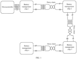
- This chip communication method based on automatic clock synchronization may be applied to the schematic diagram of an architecture of a chip communication circuit based on automatic clock synchronization shown in FIG. 1 .
- the chip communication circuit based on automatic clock synchronization includes: a controller (a microcontroller as shown in FIG. 1 ), configured to send a control instruction.
- control instruction is an ISO-SPI instruction, which is a read or write register instruction sent to the battery management chip AFE.
- the control instruction may be a voltage collection instruction, a read sampling result instruction, a balance instruction, a balance stop instruction, and so on.
- the MCU when the MCU needs to read cell voltage data, the MCU sends a voltage collection instruction the AFE and waits for the AFE to complete sampling, and sends a read sampling result instruction to the AFE to read a corresponding result.
- the MCU sends a balance instruction, and the AFE performs balancing; the MCU sends a balance stop instruction, and the AFE stops balancing.
- the fault diagnosis function also has the same mechanism, the entire process is controlled by the MCU as a scheduling role to stop and start an AFE function.
- Battery management chip 1 battery management chip 1, battery management chip 2, battery management chip 3..., battery management chip n
- battery management chip 1 battery management chip 1 and other battery management chips except for the first battery management chip (such as, battery management chip 2, battery management chip 3..., battery management chip n, etc.), where the first battery management chip is connected to the above controller through a serial peripheral interface, and a daisy chain with a sinusoidal sawtooth waveform is used for isolated communication between different battery management chips.
- the above first battery management chip is configured to determine clock synchronization information of the first battery management chip in response to the above received control instruction; replace a chip selection enable signal in the above control instruction with a clock synchronization signal carrying the clock synchronization information of the first battery management chip, to obtain a new control instruction (where other data in the original control instruction remains unchanged), and transmit the new control instruction to a subsequent battery management chip.
- the subsequent battery management chip obtains clock synchronization information from the clock synchronization signal (also known as a synchronization signal) and obtains control information from other data.
- the other battery management chips may perform automatic clock synchronization based on the clock synchronization information carried in the above new control instruction.
- FIG. 1 shows a microcontroller unit MCU and multiple battery management chips AFEs, and hardware connection interfaces between the first battery management chip AFE1 and other subsequent battery management chips AFEs.
- the connection method of the entire system is that the microcontroller unit MCU communicates with the first battery management chip AFE1 through a SPI, and the first battery management chip AFE1 and a second battery management chip AFE2, as well as all subsequent battery management chips, perform isolated communication using a daisy chain with a sinusoidal sawtooth waveform.
- each battery management chip AFE typically includes an ADC sampling module, a balance control module, a fault diagnosis module, a register module, and a data storage module.
- the ADC sampling module is mainly configured to perform voltage sampling for a cell, temperature sampling for a cell, total voltage sampling for a battery pack;
- the balance control module is used for active and passive balance control;
- the fault diagnosis module is used for fault diagnosis such as detecting a voltage collection line disconnection, a balance line disconnection, a battery over protection, etc.;
- the register module is configured to configure the AFE; and the data storage module is configured to store sampling results and system status information.
- the first battery management chip among the multiple battery management chips upon receiving a control instruction sent by the controller MCU, analyzes the control instruction to determine a chip selection enable signal in the control instruction, determines a waveform of the chip selection enable signal CS as shown in FIG. 2 , replaces the chip selection enable signal with clock synchronization information, which is automatically generated by the first battery management chip connected to the MCU, in a form of a clock synchronization signal according to falling and rising edges of the waveform of the chip selection enable signal, and transmits the new control instruction to other battery management chips among the multiple battery management chips through a daisy chain with a sinusoidal sawtooth waveform until it is transmitted to a last battery management chip.
- clock synchronization information which is automatically generated by the first battery management chip connected to the MCU
- isolated communication is performed between different battery management chips, and the daisy chain used is with a sinusoidal sawtooth wave, which has the advantages of strong signal anti-interference and easy recognition.
- the above controller is also configured to configure a scheduler mode parameter of the battery management chip and send a scheduler mode start instruction to the battery management chip, to control the above battery management chip to execute a communication task in a cyclic manner according to the above scheduler mode parameter.
- the above scheduler mode parameter includes at least one of the following: a balancing start time, a settling time after equalizing, a preparation time before self-diagnosis of a balance circuit, a preparation time before open wire self-diagnosis of a battery collection wire, and a time required for collecting battery voltage or temperature.
- scheduler mode parameters for voltage collection, temperature collection, GPIO configuration, passive balance, and fault diagnosis may be configured, and the battery management chip may be caused, by a simplified instruction, to collect data according to a configured mode.
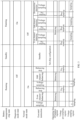
- FIG. 3 shows an optional operation timing diagram of a scheduler mode, which has been optimized and designed according to an actual operating condition to reduce power consumption of communication between battery management chips.
- battery management chip states of the battery management chip include a running state and a standby state, and diagnostic mode states of the battery management chip include an on state and an off state; normal mode states of the battery management chip includes an on state and an off state.
- commands executed by the battery management chip in the running state include but are not limited to: voltage sampling, even channel balance, balancing stop, voltage sampling, odd channel balancing, balancing stop, etc.
- the commands executed by the battery management chip in the running state may further include but are not limited to: even channel balancing (pre-sampling, voltage sampling), odd channel balancing (pre-sampling, voltage sampling), and disconnection detection (pre-sampling, voltage sampling).
- even channel balancing pre-sampling, voltage sampling
- odd channel balancing pre-sampling, voltage sampling
- disconnection detection pre-sampling, voltage sampling.
- FIG. 3 after chip configuration is set, an operating line of a balance register may be sampled and a corresponding balance processing instruction may be executed. Afterwards, a voltage pre-sampling register is sampled and a corresponding balancing stop instruction is executed, and a voltage sampling register may be sampled and a corresponding sampling instruction may be executed.
- the MCU sends a scheduler mode (scheduler system) start instruction, and the battery management chip may execute in a cyclic manner according to a scheduler cycle based on a time configured by the initialization parameters.
- Voltage information and temperature information collected in each stage are automatically stored in a register.
- voltage information and temperature information in the normal collection mode may be stored, voltage information in a self-diagnosis process of a balancing circuit may be stored, which is a data source for realizing the diagnostic function; and voltage information in an open wire self-diagnosis process of a battery collection wire (a data source for realizing the diagnostic function) may be stored.
- the battery management chip during the initialization of the battery management chip, functional parameters for voltage collection, temperature collection, GPIO configuration, passive balance, fault diagnosis, and the like are configured. Then, the battery management chip may be caused, by a simplified instruction, to collect data according to the configured mode. Compared to the MCU sending the above instructions separately to achieve these functions, it saves 60% of communication messages and can save 60% of communication power consumption.
- the MCU adopts more simplified instructions to achieve battery voltage collection, temperature collection, passive balance, and diagnostic function, reducing the quantity of instructions sent via MCU messages and thereby reducing 60% of communication power consumption.
- the synchronization of all battery collection can be guaranteed to be less than 1ms (assuming that the MCU sends an instruction to the battery management chips at least once every 1s); moreover, in the solution of the present application, isolated communication is performed between different battery management chips, and the daisy chain used is with a sinusoidal sawtooth wave, which has the advantages of strong signal anti-interference and easy recognition.
- each battery unit has multiple battery slave control units CSC to monitor voltage information and temperature information of each cell or each battery pack; the CSC may also report collected relevant information to the battery control unit BMU, and then perform cell voltage balancing according to an instruction of the BMU.
- the other battery management chips are further configured to determine whether the clock synchronization information carried in the new control instruction is the same as their own clock information each time the new control instruction is received; and calibrate their own clock information based on the clock synchronization information to perform automatic clock synchronization if it is determined that the clock synchronization information is different from their own clock information.
- the other battery management chips are further configured to determine whether the clock synchronization information carried in at least two new control instructions is the same when receiving the at least two new control instructions;, and calibrate their own clock information based on the last received clock synchronization information to perform automatic clock synchronization if it is determined that the clock synchronization information carried in the at least two new control instructions is different.
- the controller MCU can adopt more simplified instructions to control the battery management chips to achieve battery voltage collection, temperature collection, passive balance, and diagnostic function, the synchronization of all battery collection may be guaranteed to be less than 1ms (assuming that the MCU sends control instructions to the battery management chip with a maximum interval of 1 second), thereby reducing the quantity of control instructions sent via MCU messages, and reducing 60% of communication power consumption.
- a timing self-synchronization design is added.
- a data parser in the first battery management chip may analyze the control instruction to determine a chip selection enable signal in the control instruction, determine a waveform of the chip selection enable signal CS as shown in FIG. 2 , and replace the chip selection enable signal with the clock synchronization information, which is automatically generated by the first battery management chip connected to the MCU, in a form of a clock synchronization signal based on the falling and rising edges of the waveform, including but not limited to positions 0xAA and 0x55 (0xAA and 0x55 are merely taken as examples) as shown in FIG. 2 , to obtain a new control instruction.
- a daisy chain with a sinusoidal sawtooth waveform is used for isolated communication between different battery management chips.
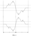
- a waveform of the sinusoidal sawtooth waveform is shown in FIG. 4
- a corresponding relationship between a pulse, a level, and a waveform in FIG. 4 is shown in Table 1.
- Vp2 2 * Vp1
- t2 2 * t1.
- Pulse name First level Second level Third level Fourth level Waveform Data sinusoidal sawtooth wave (Number 1) Vp1 (1/2 t1) Vp2 (1/2 t1) -Vp1 (1/2 t1) -Vp2 (1/2 t1) Data cosinusoidal sawtooth wave (Number 0) -Vp1 (1/2 t1) -Vp2 (1/2 t1) Vp1 (1/2 t1) Vp2 (1/2 t1) Clock synchroniza tion sinusoidal sawtooth wave (Number 1) Vp1 (1/2 t2) Vp2 (1/2 t2) -Vp1 (1/2 t2) -Vp2 (1/2 t2) Clock synchroniza tion cosinusoidal sawtooth wave (Number 0) -Vp1 (1/2 t2) -Vp2 (1/2 t2) Vp1 (1/2 t2) Vp2 (1/2 t2)
- an optional schematic circuit diagram is used to display a connection relationship between a controller and a first battery management chip.
- the controller MCU is used as a master station (a master), and the battery management chip is used as a slave station (a slave).
- the SPI is a serial peripheral interface
- the MISO is a master-in-slave-out signal line of the SPI
- MOSI is a master-out-slave-in signal line of the SPI
- the SCK is a clock signal line of the SPI
- the CS is a chip selection enable line of the SPI
- the TX represents sending, the RX represents receiving
- the SP is a high-end of a daisy chain differential communication
- the SM is a low-end of the daisy chain differential communication
- the SS is a CS signal of the SPI.
- the controller and the first battery management chip respectively include a data transmission parser, a two-stage parallel current generator, a data parser, and a timing controller.
- the data transmission parser is configured to convert a data bit 0 or 1 into a three-level sawtooth pulse with a half pulse width of t1;
- the two-stage parallel current generator is configured to generate a three-level 0V, Vp1, and Vp2 sawtooth waveforms;
- the data parser is configured to detect pulses with a pulse width of t1 received from a main port and timing controller, and trigger a comparator to compare an input voltage with two reference voltages Vp 1 and Vp2 to determine whether it is data 0 or 1;
- the timing controller is configured to control timing synchronization between multiple battery management chips.
- the master station i.e., the controller, includes a system synchronization signal generator, which is configured to fill front and back ends of the data area with a 16 bit synchronous clock synchronization signal and send to a port of the slave stations.
- each data bit has a half pulse width of t2, and it uses a two-stage current generator to generate a three-level sawtooth waveform for modulating data bits.
- the slave station i.e. the battery management chip, includes a system synchronization signal parser, configured to detect pulses with a pulse width of t2 received from the master station port and the timing controller, and if the t2 half pulse width is found, trigger a 2-level voltage comparator to determine whether the data is 0 or 1.
- a system synchronization signal parser configured to detect pulses with a pulse width of t2 received from the master station port and the timing controller, and if the t2 half pulse width is found, trigger a 2-level voltage comparator to determine whether the data is 0 or 1.
- a traditional MCU controls the battery management chips by sending relevant instructions such as voltage collection, temperature collection, GPIO configuration, balance enabling, balance disabling, fault diagnosis control, etc., via messages. There are many instructions to control the battery management chips. In the embodiments of the present application, by configuring the automatic scheduler function parameter, these instructions can be simplified. The MCU only configures the scheduler function parameters of these functions during initialization, presets behaviors and timing of these scheduling function parameters, and only periodically reads data stored in the battery management chip.
- the MCU adopts more simplified instructions to achieve battery voltage collection, temperature collection, passive balance, and diagnostic function, reducing the quantity of instructions sent via MCU messages and thereby reducing 60% of communication power consumption.
- the synchronization of all battery collection may be guaranteed to be less than 1ms (assuming that the MCU sends an instruction to the battery management chips at least once every 1s); moreover, in the present application, isolated communication is performed between different battery management chips, and the daisy chain used is with a sinusoidal sawtooth wave, which has the advantages of strong signal anti-interference and easy recognition.
- FIG. 6 is a flowchart of a chip communication method based on automatic clock synchronization provided in an embodiment of the present application. As shown in FIG. 6 , the method includes:
- control instruction is sent by a controller to the first battery management chip among multiple battery management chips through a serial peripheral interface, and a daisy chain with a sinusoidal sawtooth waveform is used for isolated communication between different battery management chips.
- the other battery management chips are battery management chips among the multiple battery management chips except for the first battery management chip.
- a daisy chain with a sinusoidal sawtooth waveform is used for isolated communication between different battery management chips, which not only has the advantages of strong anti-interference performance but also easy recognition, and thus has strong practical value and novelty.
- the first battery management chip among the multiple battery management chips upon receiving a control instruction sent by the controller MCU, may add the clock synchronization information of the first battery management chip itself to the control instruction by replacing the chip selection enable signal CS in the control instruction, and transmit the new control instruction to the other battery management chips among the multiple battery management chips through a daisy chain until it is transmitted to the last battery management chip.
- a timing self-synchronization design is added, which not only reduces the power consumption of the daisy chain communication, but also maintains the clock synchronization of the battery management chips, and achieves the technical effect of taking into consideration both communication anti-interference and signal recognition.
- isolated communication is performed between different battery management chips, and the daisy chain used is with a sinusoidal sawtooth wave, which has the advantages of strong signal anti-interference and easy recognition. It can solve the problem of high communication power consumption and unsynchronized clocks between battery management chips in existing daisy chain communication methods, and achieve the technical effect of reducing the power consumption of the daisy chain communication, maintaining the clock synchronization of the battery management chips, and taking into consideration both communication anti-interference and signal recognition.
- communication between the controller and the first battery management chip is performed using a serial peripheral interface, and isolated communication between different battery management chips is performed using a daisy chain with a sinusoidal sawtooth waveform.
- the first battery management chip determines the current clock synchronization information after receiving the control instruction, and then replaces the chip selection enable signal in the control instruction with a clock synchronization signal carrying the clock synchronization information to obtain the new control instruction, which can assist the other battery management chips in performing automatic clock synchronization based on the above clock synchronization information carried in the new control instruction.
- a traditional MCU controls the battery management chips by sending relevant instructions such as voltage collection, temperature collection, GPIO configuration, balance enabling, balance disabling, fault diagnosis control, etc., via messages. There are many instructions to control the battery management chip. In the embodiments of the present application, by configuring the automatic scheduler function parameters, these instructions can be simplified. The MCU only configures the scheduler function parameters of these functions during initialization, presets behaviors and timing of these scheduling function parameters, and only periodically reads data stored in the battery management chip.
- the chip communication method based on automatic clock synchronization further includes the following method steps:
- the above scheduler mode parameter includes at least one of the following: a balancing start time, a settling time after balancing, a preparation time before self-diagnosis of a balancing circuit, a preparation time before open wire self-diagnosis of a battery collection wire, and a time required for collecting battery voltage or temperature.
- the MCU after setting the above scheduler mode parameter, the MCU sends a scheduler mode (scheduler system) start instruction, and the battery management chip executes in a cyclic manner according to a scheduler cycle based on a time configured by the initialization parameters.
- Voltage information and temperature information collected in each stage are automatically stored in a register. For example, voltage information and temperature information under a normal collection mode may be stored, voltage information in a self-diagnosis process of a balancing circuit (a data source for realizing the diagnostic function) may be stored.
- functional parameters for voltage collection, temperature collection, GPIO configuration, passive balance, fault diagnosis, and the like are configured.
- the battery management chip may collect data according to the configured mode through simplified instructions. Compared to the MCU sending the above instructions separately to achieve these functions, it saves 60% of communication messages and can save 60% of communication power consumption.
- the MCU adopts more simplified instructions to achieve battery voltage collection, temperature collection, passive balance, and diagnostic function, reducing the quantity of instructions sent via MCU messages and thereby reducing 60% of communication power consumption.
- the synchronization of all battery collection may be guaranteed to be less than 1ms (assuming that the MCU sends an instruction to the battery management chips at least once every 1s); moreover, in the present application, isolated communication is performed between different battery management chips, and the daisy chain used is with a sinusoidal sawtooth wave, which has the advantages of strong signal anti-interference and easy recognition.
- the other battery management chips perform automatic clock synchronization based on the clock synchronization information carried in the new control instruction, which includes:
- the other battery management chips compare whether the clock synchronization information carried in the new control instruction is the same as their own clock information each time the new control instruction is received; and calibrate their own clock information based on the clock synchronization information to perform automatic clock synchronization if it is determined that the clock synchronization information is different from their own clock information.
- the above method further includes:
- the other battery management chips compare whether the clock synchronization information carried in at least two new control instructions is the same when receiving the at least two new control instructions; and calibrate their own clock information based on the last received clock synchronization information to perform automatic clock synchronization if it is determined that the clock synchronization information carried in the at least two new control instructions is different.
- the controller MCU adopts more simplified instructions to control the battery management chips to achieve functions of battery voltage collection, temperature collection, passive balance and diagnosis, the synchronization of all battery collection may be guaranteed to be less than 1ms (assuming that the MCU sends control instructions to the battery management chip with a maximum interval of 1 second), thereby reducing the quantity of control instructions sent via MCU messages, and reducing 60% of communication power consumption.
- user information including but not limited to user device information, user personal information, etc.
- data including but not limited to data used for analysis, stored data, displayed data, etc.
- user information and data involved in the present application are all information and data authorized by the user or fully authorized by all parties, and the collection, use, and processing of relevant data comply with relevant laws, regulations, and standards of relevant countries and regions.
- Corresponding operation entrances are provided for users to choose authorization or refusal.
- FIG. 7 is a structural diagram of a chip communication apparatus based on automatic clock synchronization provided in an embodiment of the present application. As shown in FIG. 7 , the apparatus includes:
- the apparatus further includes:
- the synchronization module includes:
- the apparatus further includes:
- the present application further provides an electronic device including: a processor and a memory connected to the processor;
- the present application further provides a computer-readable storage medium storing computer execution instructions, where when the computer execution instructions are used to implement any method as described above when executed by a processor.
- the present application further provides a computer program product including a computer program, where the computer program implements any method as described above when executed by a processor.
- the present application further provides an electronic device.
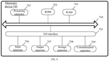
- FIG. 8 a schematic diagram of the structure of an electronic device 700 suitable for implementing an embodiment of the present application is shown, which may be a terminal device or a server.
- the electronic device 700 may include a processing apparatus (such as, a central processing unit, a graphics processor, etc.) 701, and the processing apparatus 701 may perform various appropriate actions and processing according to a program stored in a read only memory (Read only memory, ROM) 702 or a program loaded from a storage apparatus 708 into a random access memory (Random access memory, RAM) 703.
- ROM read only memory
- RAM random access memory
- Various programs and data necessary for the operation of the electronic device 700 are also stored in the RAM 703.
- the processing apparatus 701, ROM 702, and RAM 703 are connected to each other through a bus 704. And an input/output (I/O) interface 705 is also connected to the bus 704
- the following apparatuses may be connected to the I/O interface 705: an input apparatus 706 including, for example, a touch screen, a touchpad, a keyboard, a mouse, a camera, a microphone, an accelerometer, a gyroscope, etc.; an output apparatus 707 including, for example, a liquid crystal display (Liquid crystal display, LCD), a speaker, a vibrator, etc.; a storage apparatus 708 including, for example, a magnetic tape, a hard disk, etc.; and a communication apparatus 709.
- the communication apparatus 709 may allow the electronic device 700 to communicate wirelessly or by wire with other devices to exchange data.
- FIG. 8 shows the electronic device 700 having various apparatuses, it should be understood that not all of the illustrated apparatuses are required to be implemented or provided. More or fewer apparatuses may alternatively be implemented or provided.
- an embodiment of the present application includes a computer program product including a computer program carried on a computer-readable medium, where the computer program includes program code for performing the method illustrated in the respective flowcharts.
- the computer program may be downloaded and installed from a network via the communication apparatus 709, or installed from the storage apparatus 708, or installed from the ROM 702.
- the processing apparatus 701 the above functions defined in the embodiments of the present application are implemented.
- the computer-readable medium described in the present application may be a computer-readable signal medium or a computer-readable storage medium or any combination thereof.
- the computer-readable storage medium may be, for example, but not limited to, an electrical, a magnetic, an optical, an electromagnetic, an infrared, or a semiconductor system, apparatus or device, or a combination thereof.
- the computer-readable storage medium may include, but are not limited to, an electrical connection with one or more wires, a portable computer disk, a hard disk, a random-access memory (RAM), a read only memory (ROM), an erasable programmable read only memory (EPROM or flash memory), an optical fiber, a portable compact disk read only memory (CD-ROM), an optical storage device, a magnetic storage device, or any suitable combination thereof.
- the computer-readable storage medium may be any tangible medium that includes or stores a program that may be used by or used in combination with an instruction execution system, apparatus, or device.
- the computer-readable signal medium may include a data signal propagated in baseband or as part of a carrier wave, carrying computer-readable program code therein. Such propagated data signal may be in a variety of forms, including but not limited to an electromagnetic signal, an optical signal, or any suitable combination thereof.
- the computer-readable signal medium may also be any computer-readable medium other than the computer-readable storage medium, and the computer-readable signal medium can transmit, propagate, or transport the program used by or used in combination with the instruction execution system, apparatus or device.
- the program code included on the computer-readable medium may be transmitted through any suitable medium including, but not limited to, an electrical wire, an optical fiber cable, a RF (Radio Frequency), etc., or any suitable combination thereof.
- the computer-readable medium may be included in the above electronic device; and may also exist independently without being assembled into the electronic device.
- the computer-readable medium carries one or more programs, and the one or more programs, when executed by the electronic device, cause the electronic device to execute the method shown in the above embodiments.
- the computer program code for performing an operation of the present application may be written in one or more programming languages or a combination thereof, where the above programming languages include an obj ect-oriented programming language, such as Java, Smalltalk, and C++, as well as a conventional procedural programming language, such as "C" language or similar programming languages.
- the program code may be executed entirely on a user computer, executed partly on a user computer, executed as a stand-alone software package, executed partly on a user computer and partly on a remote computer, or executed entirely on a remote computer or a server.
- the remote computer may be connected to the user computer through any kind of network, including a local area network (Local Area Network, LAN) or a wide area network (Wide Area Network, WAN), or may be connected to an external computer (e.g., connected via the Internet using an Internet service provider).
- LAN Local Area Network
- WAN Wide Area Network
- each block in the flowcharts or block diagrams may represent a module, a program segment, or a portion of code that includes one or more executable instructions for implementing a specified logical function.
- functions indicated in the blocks may occur in an order different from that indicated in the figures. For example, two blocks shown in succession may, in fact, be executed substantially concurrently, or be executed in a reverse order sometimes, depending on the functionality involved.
- each block of the block diagrams and/or flowcharts, or a combination of blocks in the block diagrams and/or flowcharts may be implemented with a special-purposed hardware-based system that performs a specified function or operation, or may be implemented with a combination of special-purposed hardware and a computer instruction.
- the involved units described in embodiments of the present application may be implemented by means of software, and may also be implemented by means of hardware. Names of these units do not constitute a limitation on the units per se under certain circumstances.
- exemplary types of hardware logic components include: a field programmable gate array (Field programmable gate array, FPGA), an application specific integrated circuit (Application specific integrated circuit, ASIC), an application specific standard product (Application specific standard parts, ASSP), a system on chip (System on chip, SOC), a complex programmable logical device (Complex programmable logic device, CPLD) and more.
- FPGA field programmable gate array
- ASIC application specific integrated circuit
- ASSP application specific standard parts
- SOC System on chip
- CPLD complex programmable logical device
- a machine-readable medium may be a tangible medium that may contain or store a program for use by or in connection with an instruction execution system, apparatus or device.
- the machine-readable medium may be a machine-readable signal medium or a machine-readable storage medium.
- the machine-readable medium may include, but is not limited to, an electronic, a magnetic, an optical, an electromagnetic, an infrared, or a semiconductor system, apparatus, or device, or any suitable combination of the foregoing.
- machine-readable storage medium More specific examples of the machine-readable storage medium would include an electrical connection based on one or more wires, a portable computer disk, a hard disk, a random access memory (RAM), a read only memory (ROM), an erasable programmable read only memory (EPROM or flash memory), an optic fiber, a portable compact disk read only memory (CD-ROM), an optical storage device, a magnetic storage device, or any suitable combination of the foregoing.
- RAM random access memory
- ROM read only memory
- EPROM or flash memory erasable programmable read only memory
- CD-ROM compact disk read only memory
- magnetic storage device or any suitable combination of the foregoing.
Landscapes
- Engineering & Computer Science (AREA)
- Computer Networks & Wireless Communication (AREA)
- Signal Processing (AREA)
- Theoretical Computer Science (AREA)
- Chemical & Material Sciences (AREA)
- Chemical Kinetics & Catalysis (AREA)
- Electrochemistry (AREA)
- General Chemical & Material Sciences (AREA)
- Manufacturing & Machinery (AREA)
- Physics & Mathematics (AREA)
- General Engineering & Computer Science (AREA)
- General Physics & Mathematics (AREA)
- Microelectronics & Electronic Packaging (AREA)
- Secondary Cells (AREA)
- Power Sources (AREA)
- Dc Digital Transmission (AREA)
- Synchronisation In Digital Transmission Systems (AREA)
Abstract
Description
- The present application relates to communication technology and, in particular, to a chip communication circuit, method, and apparatus based on automatic clock synchronization.
- Existing daisy chain communication technology solutions are all achieved through converting universal serial communication into isolated serial communication of differential signals. For example, there are mainly two types: one is converting into isolated serial communication of differential signals by a universal asynchronous receiver/transmitter UART, and the other one is converting into isolated serial communication of differential signals by a serial peripheral interface SPI.
- Since the entire communication process involves a microcontroller MCU sending data to battery management chips AFEs, the communication process is mainly divided into two modes: a read mode and a write mode. However, read and the write cannot occur simultaneously on the daisy chain, and data needs to be written first before being read.
- However, the existing daisy chain communication methods have high communication power consumption and unsynchronized clocks among battery management chips, and cannot take into account both communication anti-interference and signal recognition.
- The present application provides a chip communication circuit, method, and apparatus based on automatic clock synchronization, to solve the problem of high communication power consumption and unsynchronized clocks among battery management chips in existing daisy chain communication methods, and achieve the technical effect of reducing the power consumption of the daisy chain communication, maintaining the clock synchronization of battery management chips, and taking into account both communication anti-interference and signal recognition.
- In an aspect, the present application provides a chip communication method based on automatic clock synchronization, including:
- determining clock synchronization information of a first battery management chip in response to a received control instruction, where the control instruction is sent by a controller to the first battery management chip among multiple battery management chips through a serial peripheral interface;
- replacing a chip selection enable signal in the control instruction with a clock synchronization signal carrying the clock synchronization information of the first battery management chip to obtain a new control instruction; and
- transmitting the new control instruction to other battery management chips, so that the other battery management chips perform automatic clock synchronization based on the clock synchronization information carried in the new control instruction; where the other battery management chips are battery management chips among the multiple battery management chips except for the first battery management chip, and a daisy chain with a sinusoidal sawtooth waveform is used for isolated communication between different battery management chips.
- In an optional implementation, the method further includes:
- at initialization of each of the multiple battery management chips, configuring a scheduler mode parameter of the battery management chip, where the scheduler mode parameter includes at least one of: a balancing start time, a settling time after balancing, a preparation time before self-diagnosis of a balancing circuit, a preparation time before open wire self-diagnosis of a battery collection wire, and a time required for collecting battery voltage or temperature;
- in response to a scheduler mode start instruction received by the battery management chip, executing a communication task in a cyclic manner according to the scheduler mode parameter.
- In another aspect, the present application provides a chip communication circuit based on automatic clock synchronization, including:
- a controller, configured to send a control instruction; and
- multiple battery management chips, including: a first battery management chip and other battery management chips except for the first battery management chip, where the first battery management chip is connected to the controller through a serial peripheral interface, and a daisy chain with a sinusoidal sawtooth waveform is used for isolated communication between different battery management chips;
- where the first battery management chip is configured to: determine clock synchronization information of the first battery management chip in response to the received control instruction; replace a chip selection enable signal in the control instruction with a clock synchronization signal carrying the clock synchronization information of the first battery management chip to obtain a new control instruction; and transmit the new control instruction to other battery management chips, so that the other battery management chips perform automatic clock synchronization based on the clock synchronization information carried in the new control instruction.
- In an optional implementation, at initialization of each of the multiple battery management chips, the controller is further configured to configure a scheduler mode parameter of the battery management chip, and send a scheduler mode start instruction to the battery management chip to control the battery management chip to execute a communication task in a cyclic manner according to the scheduler mode parameter, where the scheduler mode parameter includes at least one of: a balancing start time, a settling time after balancing, a preparation time before self-diagnosis of a balancing circuit, a preparation time before open wire self-diagnosis of a battery collection wire, and a time required for collecting battery voltage or temperature.
- In an optional implementation, the other battery management chips are further configured to determine whether the clock synchronization information carried in the new control instruction is the same as clock information of the other battery management chips each time the new control instruction is received; and calibrate the clock information of the other battery management chips based on the clock synchronization information to perform automatic clock synchronization if it is determined that the clock synchronization information is different from the clock information of the other battery management chips.
- In an optional implementation, the other battery management chips are further configured to determine whether the clock synchronization information carried in at least two new control instructions is the same when receiving the at least two new control instructions; and calibrate clock information of the other battery management chips based on the last received clock synchronization information to perform automatic clock synchronization if it is determined that the clock synchronization information carried in the at least two new control instructions is different.
- In another aspect, the present application provides a chip communication apparatus based on automatic clock synchronization, including:
- a determination module, configured to determine clock synchronization information of a first battery management chip in response to a received control instruction, where the control instruction is sent by a controller to the first battery management chip among multiple battery management chips through a serial peripheral interface;
- a replacement module, configured to replace a chip selection enable signal in the control instruction with a clock synchronization signal carrying the clock synchronization information of the first battery management chip to obtain a new control instruction; and
- a synchronization module, configured to transmit the new control instruction to other battery management chips, so that the other battery management chips perform automatic clock synchronization based on the clock synchronization information carried in the new control instruction; where the other battery management chips are battery management chips among the multiple battery management chips except for the first battery management chip, and a daisy chain with a sinusoidal sawtooth waveform is used for isolated communication between different battery management chips.
- In another aspect, the present application provides an electronic device including: a processor, and a memory connected to the processor; the memory stores computer execution instructions; and the processor executes the computer execution instructions stored in the memory to implement the method as described above.
- In another aspect, the present application provides a computer-readable storage medium storing computer execution instructions, where when the computer execution instructions are used to implement the method as described above when executed by a processor.
- In another aspect, the present application provides a computer program product including a computer program, where the computer program implements the method as described above when executed by a processor.
- In the chip communication circuit, method, and apparatus based on automatic clock synchronization provided in the present application, as the control instruction is sent by the controller to the first battery management chip among the multiple battery management chips through a serial peripheral interface, that is, the communication between the controller and the first battery management chip is achieved through the serial peripheral interface, the other battery management chips are battery management chips among the multiple battery management chips except for the first battery management chip, and a daisy chain with a sinusoidal sawtooth waveform is used for isolated communication between different battery management chips. Furthermore, clock synchronization information of the first battery management chip is determined in response to a received control instruction; a chip selection enable signal in the control instruction is replaced with a clock synchronization signal carrying the clock synchronization information of the first battery management chip to obtain a new control instruction; and the new control instruction is transmitted to other battery management chips, so that the other battery management chips perform automatic clock synchronization based on the clock synchronization information carried in the new control instruction.
- Therefore, in the embodiments of the present application, communication between the controller and the first battery management chip is performed using a serial peripheral interface, and isolated communication between different battery management chips is performed using a daisy chain with a sinusoidal sawtooth waveform. The first battery management chip determines the current clock synchronization information after receiving the control instruction, and then replaces the chip selection enable signal in the control instruction with a clock synchronization signal carrying the clock synchronization information to obtain the new control instruction, which can assist the other battery management chips in performing automatic clock synchronization based on the above clock synchronization information carried in the new control instruction. Moreover, isolated communication is performed between different battery management chips, and the daisy chain used is with a sinusoidal sawtooth wave, which has the advantages of strong signal anti-interference and easy recognition. It can solve the problem of high communication power consumption and unsynchronized clocks among battery management chips in existing daisy chain communication methods, and achieve the technical effect of reducing the power consumption of the daisy chain communication, maintaining the clock synchronization of battery management chips, and taking into consideration both communication anti-interference and signal recognition.
- The drawings here are incorporated into the specification and form a part of the specification, illustrating embodiments in accordance with the present application and used together with the specification to explain the principles of the present application.
-
FIG. 1 is a schematic diagram of an architecture of a chip communication circuit based on automatic clock synchronization provided in an embodiment of the present application; -
FIG. 2 is a schematic diagram of a writing position of a type of optional clock synchronization information provided in an embodiment of the present application; -
FIG. 3 is an operation timing diagram of an optional scheduler mode provided in an embodiment of the present application; -
FIG. 4 is a waveform diagram of an optional sinusoidal sawtooth waveform provided in an embodiment of the present application; -
FIG 5 is a schematic circuit diagram of a connection relationship between a controller and a first battery management chip provided in an embodiment of the present application; -
FIG. 6 is a schematic flowchart of a chip communication method based on automatic clock synchronization provided in an embodiment of the present application; -
FIG. 7 is a structural diagram of a chip communication apparatus based on automatic clock synchronization provided in an embodiment of the present application; -
FIG. 8 is a structure schematic diagram of an electronic device provided in an embodiment of the present application. - Through the above drawings, clear embodiments of the present application have been shown, and more detailed descriptions will be provided in the following. These drawings and textual descriptions illustrate the concept of the present application to those skilled in the art by referring to specific embodiments, rather than limiting the scope of the concept of the present application in any way.
- Here, illustrative embodiments will be described in detail, which are illustrated in the accompanying drawings. When the following description involves drawings, the same numbers in different drawings represent the same or similar elements unless otherwise specified. The embodiments described in the following illustrative embodiments do not represent all embodiments consistent with the present application. On the contrary, they are only examples of apparatus and methods consistent with some aspects of the present application as detailed in the attached claims.
- Firstly, terms involved in the present application is explained:
The daisy chain communication mode, refers to that a serial communication network connects like a daisy chain, hence called a daisy chain. - Battery management system (BMS): commonly known as a battery nanny or a battery manager, which is primarily designed to intelligently manage and maintain various battery units, to prevent over charging and over discharging, extend battery life, and monitor battery status.
- Battery main control unit (BMU): a core component of the battery management system, which has the function of detecting voltage of N series lithium batteries, detecting battery temperature and automatically balancing battery power, and provides an isolated CAN communication interface, and provides information of voltage, temperature, monitoring and alarm to the BMS.
- Battery slave control unit (CSC): a monitor installed on a cell, used for collecting information of this battery series and transmitting the information to the BMU for processing.
- Bus extender (GENERAL PURPOSE INPUT OUTPUT, GPIO): referring to an expansion of an IO port simplified by using an industry standard I2C, SMBUS, or SPI interface. When a microcontroller unit or a chipset does not have sufficient IO ports, or when the system requires remote serial communication or control, a GPIO product may provide additional control and monitoring functions.
- Battery management chip (Analog Front End, AFE): also known as a simulator front end, used in the new energy industry to collect voltage and temperature of a battery module and perform battery balancing, thereby achieving functions such as battery collection wire disconnection diagnosis and balancing circuit diagnosis.
- Scheduler mode (Scheduler Mode): referring to a scheduler mode of a simulation front end, which completes voltage and temperature collection, balance control, and diagnostic function of a battery module according to a specific rule.
- Serial peripheral interface (SPI): a synchronous serial communication interface specification used for chip communication.
- Master in slave out (Master In Slave Out, MISO): an antenna technology used for wireless communication, such as, in the serial peripheral interface SPI, it is a channel signal from a slave to a master to send an instruction or data.
- Master out slave in (Master Out Slave In, MOSI): a channel signal from a master to a slave to send an instruction or data.
- Differential line: referring to a signal transmission technique, the differential line should refer to a differential wiring for differential signals, two parallel and equal-length wires are used to transmit the same signals with a phase difference of 180 degrees. These two signals have the same amplitude but opposite phases. The signals transmitted on these two wires are differential signals.
- Universal asynchronous receiver/transmitter (Universal Asynchronous Receiver/Transmitter), commonly known as UART, is an asynchronous receiver/transmitter which is a part of computer hardware. It will convert data to be transmitted between serial communication and parallel communication. As a chip that converts parallel input signals into serial output signals, the UART is usually integrated into connections of other communication interfaces.
- Existing technical solutions for daisy chain communication are all achieved through converting universal serial communication into isolated serial communication of differential signals. For example, there are mainly two types: one is to use a universal asynchronous receiver/transmitter UART for conversion to isolated serial communication of differential signals, and the other one is to use a serial peripheral interface SPI for conversion to isolated serial communication of differential signals.
- In the first type, a battery main control unit BMU sends and receive data through a serial port, in an asynchronous communication mode, and after the microcontroller unit MCU sends data, a battery management chip AFE converts serial signals into differential signals designed for a daisy chain. The differential signals will be transmitted step by step through AFEs, when the differential signals reach a last AFE, the last AFE sends data that the MCU needs to read to a previous AFE, which is then transmitted step by step to a first AFE. The first AFE receives the data, converts the data into serial communication, and sends to the MCU.
- In the second type, communicating is through a SPI, with a MCU as a master and an AFE as a slave. The communication process strictly follows SPI timing. An AFE will transmit data to the MCU at a next SPI clock signal (SCK) after the MCU completes sending. The waveform on the daisy chain is specially designed to convert 4-wire SPI signals into 2-wire differential signals for transmission. In order to meet the SPI timing between the MCU and the first AFE or Transfer, this type will design a baud rate of the daisy chain to be twice the SPI baud rate.
- In order to solve the above problems, in embodiments of the present application, a configurable automatic scheduler system is added for the battery management chip, through the multi-chip clock self- synchronization technology, a daisy chain physical layer solution of multi-chip clock self-synchronization technology is implemented.
- In embodiments of the present application, a configurable automatic scheduler system (scheduler system) is added on the basis of the traditional battery management chip AFE. In this mode, the scheduler may automatically schedule functions, such as, voltage collection, temperature collection, bus extender GPIO configuration, balance enabling, balance disabling, and fault diagnosis, and etc. Among them, the controller MCU needs to first configure the scheduler system, and then turn on the scheduler system. Since there may be various combinations of constituent units and specific timing in scheduling, the present application only uses a following combination as an example. However, the method in the embodiments of the present application may be applied to all other automatic scheduler systems.
- Below are specific embodiments to provide a detailed explanation of the technical solution of the present application and how the technical solution of the present application solves the above-mentioned technical problems. The following specific embodiments can be combined with each other, and similar concepts or processes may not be repeated in some embodiments. The following will describe the embodiments of the present application with reference to the accompanying drawings.
- The chip communication method based on automatic clock synchronization provided in the present application aims to solve the above-mentioned technical problems of the existing technology. This chip communication method based on automatic clock synchronization may be applied to the schematic diagram of an architecture of a chip communication circuit based on automatic clock synchronization shown in
FIG. 1 . As shown inFIG. 1 , the chip communication circuit based on automatic clock synchronization includes:
a controller (a microcontroller as shown inFIG. 1 ), configured to send a control instruction. - Optionally, the above control instruction is an ISO-SPI instruction, which is a read or write register instruction sent to the battery management chip AFE. For example, the control instruction may be a voltage collection instruction, a read sampling result instruction, a balance instruction, a balance stop instruction, and so on.
- In an optional embodiment, for example, when the MCU needs to read cell voltage data, the MCU sends a voltage collection instruction the AFE and waits for the AFE to complete sampling, and sends a read sampling result instruction to the AFE to read a corresponding result. For another example, the MCU sends a balance instruction, and the AFE performs balancing; the MCU sends a balance stop instruction, and the AFE stops balancing. In addition, the fault diagnosis function also has the same mechanism, the entire process is controlled by the MCU as a scheduling role to stop and start an AFE function.
- Multiple battery management chips (
battery management chip 1,battery management chip 2,battery management chip 3..., battery management chip n), including: a firstbattery management chip 1 and other battery management chips except for the first battery management chip (such as,battery management chip 2,battery management chip 3..., battery management chip n, etc.), where the first battery management chip is connected to the above controller through a serial peripheral interface, and a daisy chain with a sinusoidal sawtooth waveform is used for isolated communication between different battery management chips. - The above first battery management chip is configured to determine clock synchronization information of the first battery management chip in response to the above received control instruction; replace a chip selection enable signal in the above control instruction with a clock synchronization signal carrying the clock synchronization information of the first battery management chip, to obtain a new control instruction (where other data in the original control instruction remains unchanged), and transmit the new control instruction to a subsequent battery management chip. The subsequent battery management chip obtains clock synchronization information from the clock synchronization signal (also known as a synchronization signal) and obtains control information from other data. By transmitting the above new control instruction to other battery management chips, the other battery management chips may perform automatic clock synchronization based on the clock synchronization information carried in the above new control instruction.
-
FIG. 1 shows a microcontroller unit MCU and multiple battery management chips AFEs, and hardware connection interfaces between the first battery management chip AFE1 and other subsequent battery management chips AFEs. The connection method of the entire system is that the microcontroller unit MCU communicates with the first battery management chip AFE1 through a SPI, and the first battery management chip AFE1 and a second battery management chip AFE2, as well as all subsequent battery management chips, perform isolated communication using a daisy chain with a sinusoidal sawtooth waveform. - In an optional embodiment, each battery management chip AFE typically includes an ADC sampling module, a balance control module, a fault diagnosis module, a register module, and a data storage module. The ADC sampling module is mainly configured to perform voltage sampling for a cell, temperature sampling for a cell, total voltage sampling for a battery pack; the balance control module is used for active and passive balance control; the fault diagnosis module is used for fault diagnosis such as detecting a voltage collection line disconnection, a balance line disconnection, a battery over protection, etc.; the register module is configured to configure the AFE; and the data storage module is configured to store sampling results and system status information.
- In the present embodiment, the first battery management chip among the multiple battery management chips, upon receiving a control instruction sent by the controller MCU, analyzes the control instruction to determine a chip selection enable signal in the control instruction, determines a waveform of the chip selection enable signal CS as shown in
FIG. 2 , replaces the chip selection enable signal with clock synchronization information, which is automatically generated by the first battery management chip connected to the MCU, in a form of a clock synchronization signal according to falling and rising edges of the waveform of the chip selection enable signal, and transmits the new control instruction to other battery management chips among the multiple battery management chips through a daisy chain with a sinusoidal sawtooth waveform until it is transmitted to a last battery management chip. In this way, automatic timing synchronization can be achieved among multiple battery management chips. - In the embodiment of the present application, isolated communication is performed between different battery management chips, and the daisy chain used is with a sinusoidal sawtooth wave, which has the advantages of strong signal anti-interference and easy recognition.
- In an optional implementation, at initialization of each of the multiple battery management chips, the above controller is also configured to configure a scheduler mode parameter of the battery management chip and send a scheduler mode start instruction to the battery management chip, to control the above battery management chip to execute a communication task in a cyclic manner according to the above scheduler mode parameter.
- In an example, the above scheduler mode parameter includes at least one of the following: a balancing start time, a settling time after equalizing, a preparation time before self-diagnosis of a balance circuit, a preparation time before open wire self-diagnosis of a battery collection wire, and a time required for collecting battery voltage or temperature.
- In an embodiment of the present application, during the initialization of the battery management chip, scheduler mode parameters for voltage collection, temperature collection, GPIO configuration, passive balance, and fault diagnosis may be configured, and the battery management chip may be caused, by a simplified instruction, to collect data according to a configured mode.
-
FIG. 3 shows an optional operation timing diagram of a scheduler mode, which has been optimized and designed according to an actual operating condition to reduce power consumption of communication between battery management chips. As shown inFIG. 3 , battery management chip states of the battery management chip include a running state and a standby state, and diagnostic mode states of the battery management chip include an on state and an off state; normal mode states of the battery management chip includes an on state and an off state. InFIG. 3 , commands executed by the battery management chip in the running state include but are not limited to: voltage sampling, even channel balance, balancing stop, voltage sampling, odd channel balancing, balancing stop, etc. After a standby state, the commands executed by the battery management chip in the running state may further include but are not limited to: even channel balancing (pre-sampling, voltage sampling), odd channel balancing (pre-sampling, voltage sampling), and disconnection detection (pre-sampling, voltage sampling). As shown inFIG. 3 , after chip configuration is set, an operating line of a balance register may be sampled and a corresponding balance processing instruction may be executed. Afterwards, a voltage pre-sampling register is sampled and a corresponding balancing stop instruction is executed, and a voltage sampling register may be sampled and a corresponding sampling instruction may be executed. - In an example, after the above scheduler mode parameters are set, the MCU sends a scheduler mode (scheduler system) start instruction, and the battery management chip may execute in a cyclic manner according to a scheduler cycle based on a time configured by the initialization parameters. Voltage information and temperature information collected in each stage are automatically stored in a register. For example, voltage information and temperature information in the normal collection mode may be stored, voltage information in a self-diagnosis process of a balancing circuit may be stored, which is a data source for realizing the diagnostic function; and voltage information in an open wire self-diagnosis process of a battery collection wire (a data source for realizing the diagnostic function) may be stored. In an embodiment of the present application, during the initialization of the battery management chip, functional parameters for voltage collection, temperature collection, GPIO configuration, passive balance, fault diagnosis, and the like are configured. Then, the battery management chip may be caused, by a simplified instruction, to collect data according to the configured mode. Compared to the MCU sending the above instructions separately to achieve these functions, it saves 60% of communication messages and can save 60% of communication power consumption.
- In the embodiment of the present application, the MCU adopts more simplified instructions to achieve battery voltage collection, temperature collection, passive balance, and diagnostic function, reducing the quantity of instructions sent via MCU messages and thereby reducing 60% of communication power consumption. By using multi-chip clock self-synchronization technology, the synchronization of all battery collection can be guaranteed to be less than 1ms (assuming that the MCU sends an instruction to the battery management chips at least once every 1s); moreover, in the solution of the present application, isolated communication is performed between different battery management chips, and the daisy chain used is with a sinusoidal sawtooth wave, which has the advantages of strong signal anti-interference and easy recognition.
- In an optional embodiment, each battery unit has multiple battery slave control units CSC to monitor voltage information and temperature information of each cell or each battery pack; the CSC may also report collected relevant information to the battery control unit BMU, and then perform cell voltage balancing according to an instruction of the BMU.
- In an optional embodiment, the other battery management chips are further configured to determine whether the clock synchronization information carried in the new control instruction is the same as their own clock information each time the new control instruction is received; and calibrate their own clock information based on the clock synchronization information to perform automatic clock synchronization if it is determined that the clock synchronization information is different from their own clock information.
- In another optional embodiment, the other battery management chips are further configured to determine whether the clock synchronization information carried in at least two new control instructions is the same when receiving the at least two new control instructions;, and calibrate their own clock information based on the last received clock synchronization information to perform automatic clock synchronization if it is determined that the clock synchronization information carried in the at least two new control instructions is different.
- In the daisy-chain communication mode with automatic clock synchronization provided in the embodiment of the present application, the controller MCU can adopt more simplified instructions to control the battery management chips to achieve battery voltage collection, temperature collection, passive balance, and diagnostic function, the synchronization of all battery collection may be guaranteed to be less than 1ms (assuming that the MCU sends control instructions to the battery management chip with a maximum interval of 1 second), thereby reducing the quantity of control instructions sent via MCU messages, and reducing 60% of communication power consumption.
- In an optional embodiment, in the daisy chain communication technology of the embodiment of the present application, a timing self-synchronization design is added. After the first battery management chip receives a control instruction from the controller, a data parser in the first battery management chip may analyze the control instruction to determine a chip selection enable signal in the control instruction, determine a waveform of the chip selection enable signal CS as shown in
FIG. 2 , and replace the chip selection enable signal with the clock synchronization information, which is automatically generated by the first battery management chip connected to the MCU, in a form of a clock synchronization signal based on the falling and rising edges of the waveform, including but not limited to positions 0xAA and 0x55 (0xAA and 0x55 are merely taken as examples) as shown inFIG. 2 , to obtain a new control instruction. - In an embodiment of the present application, a daisy chain with a sinusoidal sawtooth waveform is used for isolated communication between different battery management chips. In an example, a waveform of the sinusoidal sawtooth waveform is shown in
FIG. 4 , and a corresponding relationship between a pulse, a level, and a waveform inFIG. 4 is shown in Table 1. For a design of the voltage, Vp2=2 * Vp1, and for a design of time, t2=2 * t1.Pulse name First level Second level Third level Fourth level Waveform Data sinusoidal sawtooth wave (Number 1) Vp1 (1/2 t1) Vp2 (1/2 t1) -Vp1 (1/2 t1) -Vp2 (1/2 t1) 
Data cosinusoidal sawtooth wave (Number 0) -Vp1 (1/2 t1) -Vp2 (1/2 t1) Vp1 (1/2 t1) Vp2 (1/2 t1) 
Clock synchroniza tion sinusoidal sawtooth wave (Number 1) Vp1 (1/2 t2) Vp2 (1/2 t2) -Vp1 (1/2 t2) -Vp2 (1/2 t2) 
Clock synchroniza tion cosinusoidal sawtooth wave (Number 0) -Vp1 (1/2 t2) -Vp2 (1/2 t2) Vp1 (1/2 t2) Vp2 (1/2 t2) 
- In an optional embodiment, as shown in
FIG. 5 , an optional schematic circuit diagram is used to display a connection relationship between a controller and a first battery management chip. In an embodiment of the present application, the controller MCU is used as a master station (a master), and the battery management chip is used as a slave station (a slave). Among them, the SPI is a serial peripheral interface, the MISO is a master-in-slave-out signal line of the SPI, and MOSI is a master-out-slave-in signal line of the SPI; the SCK is a clock signal line of the SPI, and the CS is a chip selection enable line of the SPI; the TX represents sending, the RX represents receiving; the SP is a high-end of a daisy chain differential communication, the SM is a low-end of the daisy chain differential communication, and the SS is a CS signal of the SPI. - As shown in
FIG. 5 , the controller and the first battery management chip respectively include a data transmission parser, a two-stage parallel current generator, a data parser, and a timing controller. Among them, the data transmission parser is configured to convert adata bit reference voltages Vp 1 and Vp2 to determine whether it isdata - In addition, the master station, i.e., the controller, includes a system synchronization signal generator, which is configured to fill front and back ends of the data area with a 16 bit synchronous clock synchronization signal and send to a port of the slave stations. Among them, each data bit has a half pulse width of t2, and it uses a two-stage current generator to generate a three-level sawtooth waveform for modulating data bits.
- The slave station, i.e. the battery management chip, includes a system synchronization signal parser, configured to detect pulses with a pulse width of t2 received from the master station port and the timing controller, and if the t2 half pulse width is found, trigger a 2-level voltage comparator to determine whether the data is 0 or 1.
- A traditional MCU controls the battery management chips by sending relevant instructions such as voltage collection, temperature collection, GPIO configuration, balance enabling, balance disabling, fault diagnosis control, etc., via messages. There are many instructions to control the battery management chips. In the embodiments of the present application, by configuring the automatic scheduler function parameter, these instructions can be simplified. The MCU only configures the scheduler function parameters of these functions during initialization, presets behaviors and timing of these scheduling function parameters, and only periodically reads data stored in the battery management chip.
- In the embodiment of the present application, the MCU adopts more simplified instructions to achieve battery voltage collection, temperature collection, passive balance, and diagnostic function, reducing the quantity of instructions sent via MCU messages and thereby reducing 60% of communication power consumption. By using multi-chip clock self-synchronization technology, the synchronization of all battery collection may be guaranteed to be less than 1ms (assuming that the MCU sends an instruction to the battery management chips at least once every 1s); moreover, in the present application, isolated communication is performed between different battery management chips, and the daisy chain used is with a sinusoidal sawtooth wave, which has the advantages of strong signal anti-interference and easy recognition.
- An embodiment of the present application further proposes an embodiment of a chip communication method based on automatic clock synchronization.
FIG. 6 is a flowchart of a chip communication method based on automatic clock synchronization provided in an embodiment of the present application. As shown inFIG. 6 , the method includes: - S101, determining clock synchronization information of a first battery management chip in response to a received control instruction.
-
S 102, replacing a chip selection enable signal in the control instruction with a clock synchronization signal carrying the clock synchronization information of the first battery management chip to obtain a new control instruction. - S103, transmitting the new control instruction to other battery management chips, so that the other battery management chips performs automatic clock synchronization based on the clock synchronization information carried in the new control instruction.
- In an example, the control instruction is sent by a controller to the first battery management chip among multiple battery management chips through a serial peripheral interface, and a daisy chain with a sinusoidal sawtooth waveform is used for isolated communication between different battery management chips.
- Optionally, the other battery management chips are battery management chips among the multiple battery management chips except for the first battery management chip.
- Unlike traditional sine waves or square waves (although sine waves have slightly better anti-interference performance, they are not easy to be analyzed and recognized by chips, which can easily cause waveform misjudgment; and square waves are easy to be recognized but have poor anti-interference performance, and are prone to waveform distortion), in the embodiment of the present application, a daisy chain with a sinusoidal sawtooth waveform is used for isolated communication between different battery management chips, which not only has the advantages of strong anti-interference performance but also easy recognition, and thus has strong practical value and novelty.
- In an embodiment of the present application, the first battery management chip among the multiple battery management chips, upon receiving a control instruction sent by the controller MCU, may add the clock synchronization information of the first battery management chip itself to the control instruction by replacing the chip selection enable signal CS in the control instruction, and transmit the new control instruction to the other battery management chips among the multiple battery management chips through a daisy chain until it is transmitted to the last battery management chip.
- In the daisy chain communication technology of an embodiment of the present application, a timing self-synchronization design is added, which not only reduces the power consumption of the daisy chain communication, but also maintains the clock synchronization of the battery management chips, and achieves the technical effect of taking into consideration both communication anti-interference and signal recognition.
- More importantly, isolated communication is performed between different battery management chips, and the daisy chain used is with a sinusoidal sawtooth wave, which has the advantages of strong signal anti-interference and easy recognition. It can solve the problem of high communication power consumption and unsynchronized clocks between battery management chips in existing daisy chain communication methods, and achieve the technical effect of reducing the power consumption of the daisy chain communication, maintaining the clock synchronization of the battery management chips, and taking into consideration both communication anti-interference and signal recognition.
- In the embodiments of the present application, communication between the controller and the first battery management chip is performed using a serial peripheral interface, and isolated communication between different battery management chips is performed using a daisy chain with a sinusoidal sawtooth waveform. The first battery management chip determines the current clock synchronization information after receiving the control instruction, and then replaces the chip selection enable signal in the control instruction with a clock synchronization signal carrying the clock synchronization information to obtain the new control instruction, which can assist the other battery management chips in performing automatic clock synchronization based on the above clock synchronization information carried in the new control instruction. It can solve the problem of high communication power consumption and unsynchronized clocks among battery management chips in existing daisy chain communication methods, and achieve the technical effect of reducing the power consumption of the daisy chain communication, maintaining the clock synchronization of each battery management chip, and taking into consideration both communication anti-interference and signal recognition.
- A traditional MCU controls the battery management chips by sending relevant instructions such as voltage collection, temperature collection, GPIO configuration, balance enabling, balance disabling, fault diagnosis control, etc., via messages. There are many instructions to control the battery management chip. In the embodiments of the present application, by configuring the automatic scheduler function parameters, these instructions can be simplified. The MCU only configures the scheduler function parameters of these functions during initialization, presets behaviors and timing of these scheduling function parameters, and only periodically reads data stored in the battery management chip.
- In an optional implementation, before determining clock synchronization information of the first battery management chip in response to the received control instruction, the chip communication method based on automatic clock synchronization further includes the following method steps:
- at initialization of each of the multiple battery management chips, configuring a scheduler mode parameter of the battery management chip; and
- in response to a scheduler mode start instruction received by the battery management chip, executing a communication task in a cyclic manner according to the scheduler mode parameter.
- In an example, the above scheduler mode parameter includes at least one of the following: a balancing start time, a settling time after balancing, a preparation time before self-diagnosis of a balancing circuit, a preparation time before open wire self-diagnosis of a battery collection wire, and a time required for collecting battery voltage or temperature.
- In an example, after setting the above scheduler mode parameter, the MCU sends a scheduler mode (scheduler system) start instruction, and the battery management chip executes in a cyclic manner according to a scheduler cycle based on a time configured by the initialization parameters. Voltage information and temperature information collected in each stage are automatically stored in a register. For example, voltage information and temperature information under a normal collection mode may be stored, voltage information in a self-diagnosis process of a balancing circuit (a data source for realizing the diagnostic function) may be stored. In an embodiment of the present application, during the initialization of the battery management chip, functional parameters for voltage collection, temperature collection, GPIO configuration, passive balance, fault diagnosis, and the like are configured. And the battery management chip may collect data according to the configured mode through simplified instructions. Compared to the MCU sending the above instructions separately to achieve these functions, it saves 60% of communication messages and can save 60% of communication power consumption.
- In the embodiment of the present application, the MCU adopts more simplified instructions to achieve battery voltage collection, temperature collection, passive balance, and diagnostic function, reducing the quantity of instructions sent via MCU messages and thereby reducing 60% of communication power consumption. By using multi-chip clock self-synchronization technology, the synchronization of all battery collection may be guaranteed to be less than 1ms (assuming that the MCU sends an instruction to the battery management chips at least once every 1s); moreover, in the present application, isolated communication is performed between different battery management chips, and the daisy chain used is with a sinusoidal sawtooth wave, which has the advantages of strong signal anti-interference and easy recognition.
- In an optional implementation, the other battery management chips perform automatic clock synchronization based on the clock synchronization information carried in the new control instruction, which includes:
- the other battery management chips compare whether the clock synchronization information carried in the new control instruction is the same as their own clock information each time the new control instruction is received; and
- calibrate their own clock information based on the clock synchronization information to perform automatic clock synchronization if it is determined that the clock synchronization information is different from their own clock information.
- In an optional embodiment, the other battery management chips compare whether the clock synchronization information carried in the new control instruction is the same as their own clock information each time the new control instruction is received; and calibrate their own clock information based on the clock synchronization information to perform automatic clock synchronization if it is determined that the clock synchronization information is different from their own clock information.
- In an optional implementation, the above method further includes:
- comparing whether the clock synchronization information carried in at least two new control instructions is the same when receiving the at least two new control instructions; and
- calibrating their own clock information based on the last received clock synchronization information to perform automatic clock synchronization if it is determined that the clock synchronization information carried in the at least two new control instructions is different.
- In another optional embodiment, the other battery management chips compare whether the clock synchronization information carried in at least two new control instructions is the same when receiving the at least two new control instructions; and calibrate their own clock information based on the last received clock synchronization information to perform automatic clock synchronization if it is determined that the clock synchronization information carried in the at least two new control instructions is different.
- In the daisy-chain communication mode with automatic clock synchronization provided in the embodiment of the present application, the controller MCU adopts more simplified instructions to control the battery management chips to achieve functions of battery voltage collection, temperature collection, passive balance and diagnosis, the synchronization of all battery collection may be guaranteed to be less than 1ms (assuming that the MCU sends control instructions to the battery management chip with a maximum interval of 1 second), thereby reducing the quantity of control instructions sent via MCU messages, and reducing 60% of communication power consumption.
- It should be noted that, user information (including but not limited to user device information, user personal information, etc.) and data (including but not limited to data used for analysis, stored data, displayed data, etc.) involved in the present application are all information and data authorized by the user or fully authorized by all parties, and the collection, use, and processing of relevant data comply with relevant laws, regulations, and standards of relevant countries and regions. Corresponding operation entrances are provided for users to choose authorization or refusal.
- According to one or more embodiments of the present application, a chip communication apparatus based on automatic clock synchronization is provided.
FIG. 7 is a structural diagram of a chip communication apparatus based on automatic clock synchronization provided in an embodiment of the present application. As shown inFIG. 7 , the apparatus includes: - a
determination module 601, configured to determine clock synchronization information of a first battery management chip in response to a received control instruction, where the control instruction is sent by a controller to the first battery management chip among multiple battery management chips through a serial peripheral interface; - a
replacement module 602, configured to replace a chip selection enable signal in the control instruction with a clock synchronization signal carrying the clock synchronization information of the first battery management chip to obtain a new control instruction; and - a
synchronization module 603, configured to transmit the new control instruction to other battery management chips, so that the other battery management chips perform automatic clock synchronization based on the clock synchronization information carried in the new control instruction; where the other battery management chips are battery management chips among the multiple battery management chips except for the first battery management chip, and a daisy chain with a sinusoidal sawtooth waveform is used for isolated communication between different battery management chips. - According to one or more embodiments of the present application, the apparatus further includes:
- a configuration module, configured to configure, at initialization of each of the multiple battery management chips, a scheduler mode parameter of the battery management chip, where the scheduler mode parameter includes at least one of: a balancing start time, a settling time after balancing, a preparation time before self-diagnosis of a balancing circuit, a preparation time before open wire self-diagnosis of a battery collection wire, and a time required for collecting battery voltage or temperature; and
- an execution module, configured to execute, in response to a scheduler mode start instruction received by the battery management chip, a communication task in a cyclic manner according to the scheduler mode parameter.
- According to one or more embodiments of the present application, the synchronization module includes:
- a comparison unit, configured to compare whether the clock synchronization information carried in the new control instruction is the same as their own clock information each time the new control instruction is received by the other battery management chips; and
- a synchronization unit, configured to calibrate their own clock information based on the clock synchronization information to perform automatic clock synchronization if it is determined that the clock synchronization information is different from their own clock information.
- According to one or more embodiments of the present application, the apparatus further includes:
- a comparison module, configured to compare whether the clock synchronization information carried in at least two new control instructions is the same when the other battery management chips receive the at least two new control instructions; and
- a calibrated synchronization module, configured to calibrate their own clock information based on the last received clock synchronization information to perform automatic clock synchronization if it is determined that the clock synchronization information carried in the at least two new control instructions is different.
- In an illustrative embodiment, the present application further provides an electronic device including: a processor and a memory connected to the processor;
- where the memory stores computer execution instructions; and
- the processor executes the computer execution instructions stored in the memory to implement any method as described above.
- In an illustrative embodiment, the present application further provides a computer-readable storage medium storing computer execution instructions, where when the computer execution instructions are used to implement any method as described above when executed by a processor.
- In an illustrative embodiment, the present application further provides a computer program product including a computer program, where the computer program implements any method as described above when executed by a processor.
- In order to achieve the above embodiments, the present application further provides an electronic device. Referring to
FIG. 8 , a schematic diagram of the structure of anelectronic device 700 suitable for implementing an embodiment of the present application is shown, which may be a terminal device or a server. - As shown in
FIG. 8 , theelectronic device 700 may include a processing apparatus (such as, a central processing unit, a graphics processor, etc.) 701, and theprocessing apparatus 701 may perform various appropriate actions and processing according to a program stored in a read only memory (Read only memory, ROM) 702 or a program loaded from astorage apparatus 708 into a random access memory (Random access memory, RAM) 703. Various programs and data necessary for the operation of theelectronic device 700 are also stored in theRAM 703. Theprocessing apparatus 701,ROM 702, andRAM 703 are connected to each other through abus 704. And an input/output (I/O)interface 705 is also connected to thebus 704 - Generally, the following apparatuses may be connected to the I/O interface 705: an
input apparatus 706 including, for example, a touch screen, a touchpad, a keyboard, a mouse, a camera, a microphone, an accelerometer, a gyroscope, etc.; anoutput apparatus 707 including, for example, a liquid crystal display (Liquid crystal display, LCD), a speaker, a vibrator, etc.; astorage apparatus 708 including, for example, a magnetic tape, a hard disk, etc.; and acommunication apparatus 709. Thecommunication apparatus 709 may allow theelectronic device 700 to communicate wirelessly or by wire with other devices to exchange data. AlthoughFIG. 8 shows theelectronic device 700 having various apparatuses, it should be understood that not all of the illustrated apparatuses are required to be implemented or provided. More or fewer apparatuses may alternatively be implemented or provided. - Specially, according to an embodiment of the present application, the processes described above with reference to the flowcharts may be implemented as a computer software program. For example, an embodiment of the present application includes a computer program product including a computer program carried on a computer-readable medium, where the computer program includes program code for performing the method illustrated in the respective flowcharts. In such an embodiment, the computer program may be downloaded and installed from a network via the
communication apparatus 709, or installed from thestorage apparatus 708, or installed from theROM 702. When the computer program is executed by theprocessing apparatus 701, the above functions defined in the embodiments of the present application are implemented. - It should be noted that the computer-readable medium described in the present application may be a computer-readable signal medium or a computer-readable storage medium or any combination thereof. The computer-readable storage medium may be, for example, but not limited to, an electrical, a magnetic, an optical, an electromagnetic, an infrared, or a semiconductor system, apparatus or device, or a combination thereof. More specific examples of the computer-readable storage medium may include, but are not limited to, an electrical connection with one or more wires, a portable computer disk, a hard disk, a random-access memory (RAM), a read only memory (ROM), an erasable programmable read only memory (EPROM or flash memory), an optical fiber, a portable compact disk read only memory (CD-ROM), an optical storage device, a magnetic storage device, or any suitable combination thereof. In the present application, the computer-readable storage medium may be any tangible medium that includes or stores a program that may be used by or used in combination with an instruction execution system, apparatus, or device. And in the present application, the computer-readable signal medium may include a data signal propagated in baseband or as part of a carrier wave, carrying computer-readable program code therein. Such propagated data signal may be in a variety of forms, including but not limited to an electromagnetic signal, an optical signal, or any suitable combination thereof. The computer-readable signal medium may also be any computer-readable medium other than the computer-readable storage medium, and the computer-readable signal medium can transmit, propagate, or transport the program used by or used in combination with the instruction execution system, apparatus or device. The program code included on the computer-readable medium may be transmitted through any suitable medium including, but not limited to, an electrical wire, an optical fiber cable, a RF (Radio Frequency), etc., or any suitable combination thereof.
- The computer-readable medium may be included in the above electronic device; and may also exist independently without being assembled into the electronic device.
- The computer-readable medium carries one or more programs, and the one or more programs, when executed by the electronic device, cause the electronic device to execute the method shown in the above embodiments.
- The computer program code for performing an operation of the present application may be written in one or more programming languages or a combination thereof, where the above programming languages include an obj ect-oriented programming language, such as Java, Smalltalk, and C++, as well as a conventional procedural programming language, such as "C" language or similar programming languages. The program code may be executed entirely on a user computer, executed partly on a user computer, executed as a stand-alone software package, executed partly on a user computer and partly on a remote computer, or executed entirely on a remote computer or a server. In a case involving the remote computer, the remote computer may be connected to the user computer through any kind of network, including a local area network (Local Area Network, LAN) or a wide area network (Wide Area Network, WAN), or may be connected to an external computer (e.g., connected via the Internet using an Internet service provider).
- The flowcharts and block diagrams in the figures illustrate the architecture, functionality, and operation of possible implementations of systems, methods and computer program products according to various embodiments of the present application. In this regard, each block in the flowcharts or block diagrams may represent a module, a program segment, or a portion of code that includes one or more executable instructions for implementing a specified logical function. Furthermore, it should be noted that, in some alternative implementations, functions indicated in the blocks may occur in an order different from that indicated in the figures. For example, two blocks shown in succession may, in fact, be executed substantially concurrently, or be executed in a reverse order sometimes, depending on the functionality involved. It should also be noted that each block of the block diagrams and/or flowcharts, or a combination of blocks in the block diagrams and/or flowcharts may be implemented with a special-purposed hardware-based system that performs a specified function or operation, or may be implemented with a combination of special-purposed hardware and a computer instruction.
- The involved units described in embodiments of the present application may be implemented by means of software, and may also be implemented by means of hardware. Names of these units do not constitute a limitation on the units per se under certain circumstances.
- The foregoing functions described herein may be executed, at least in part, by one or more hardware logic components. For example, without limitation, exemplary types of hardware logic components that may be used include: a field programmable gate array (Field programmable gate array, FPGA), an application specific integrated circuit (Application specific integrated circuit, ASIC), an application specific standard product (Application specific standard parts, ASSP), a system on chip (System on chip, SOC), a complex programmable logical device (Complex programmable logic device, CPLD) and more.
- In the context of the present application, a machine-readable medium may be a tangible medium that may contain or store a program for use by or in connection with an instruction execution system, apparatus or device. The machine-readable medium may be a machine-readable signal medium or a machine-readable storage medium. The machine-readable medium may include, but is not limited to, an electronic, a magnetic, an optical, an electromagnetic, an infrared, or a semiconductor system, apparatus, or device, or any suitable combination of the foregoing. More specific examples of the machine-readable storage medium would include an electrical connection based on one or more wires, a portable computer disk, a hard disk, a random access memory (RAM), a read only memory (ROM), an erasable programmable read only memory (EPROM or flash memory), an optic fiber, a portable compact disk read only memory (CD-ROM), an optical storage device, a magnetic storage device, or any suitable combination of the foregoing.
- The person skilled in the field will easily come up with other embodiments of the present application after considering the specification and practicing the invention disclosed herein. The present application aims to cover any variations, uses, or adaptive changes of the present application, which follow the general principles of the present application and include common knowledge or conventional technical means in the technical field not disclosed in the present application. The specification and embodiments are only considered illustrative, and the true scope and spirit of the present application are indicated in the following claims.
- It should be understood that the present application is not limited to the precise structure described above and shown in the drawings, and various modifications and changes may be made without departing from its scope. The scope of the present application is limited only by the accompanying claims.
Claims (10)
- A chip communication circuit based on automatic clock synchronization, comprising:a controller, configured to send a control instruction; andmultiple battery management chips, comprising: a first battery management chip and other battery management chips except for the first battery management chip, wherein the first battery management chip is connected to the controller through a serial peripheral interface, and a daisy chain with a sinusoidal sawtooth waveform is used for isolated communication between different battery management chips;wherein the first battery management chip is configured to: determine clock synchronization information of the first battery management chip in response to the received control instruction; replace a chip selection enable signal in the control instruction with a clock synchronization signal carrying the clock synchronization information of the first battery management chip to obtain a new control instruction; and transmit the new control instruction to other battery management chips, so that the other battery management chips perform automatic clock synchronization based on the clock synchronization information carried in the new control instruction.
- The chip communication circuit according to claim 1, wherein
at initialization of each of the multiple battery management chips, the controller is further configured to configure a scheduler mode parameter of the battery management chip, and send a scheduler mode start instruction to the battery management chip to control the battery management chip to execute a communication task in a cyclic manner according to the scheduler mode parameter, wherein the scheduler mode parameter comprises at least one of: a balancing start time, a settling time after balancing, a preparation time before self-diagnosis of a balancing circuit, a preparation time before open wire self-diagnosis of a battery collection wire, and a time required for collecting battery voltage or temperature. - The chip communication circuit according to claim 1 or 2, wherein
the other battery management chips is further configured to determine whether the clock synchronization information carried in the new control instruction is the same as clock information of the other battery management chips each time the new control instruction is received; and calibrate the clock information of the other battery management chips based on the clock synchronization information to perform automatic clock synchronization if it is determined that the clock synchronization information is different from the clock information of the other battery management chips. - The chip communication circuit according to any one of claims 1 to 3, wherein
the other battery management chips are further configured to determine whether the clock synchronization information carried in at least two new control instructions is the same when receiving the at least two new control instructions; and calibrate clock information of the other battery management chips based on the last received clock synchronization information to perform automatic clock synchronization if it is determined that the clock synchronization information carried in the at least two new control instructions is different. - A chip communication method based on automatic clock synchronization, comprising:determining (S101) clock synchronization information of a first battery management chip in response to a received control instruction, wherein the control instruction is sent by a controller to the first battery management chip among multiple battery management chips through a serial peripheral interface;replacing (S102) a chip selection enable signal in the control instruction with a clock synchronization signal carrying the clock synchronization information of the first battery management chip to obtain a new control instruction; andtransmitting (S103) the new control instruction to other battery management chips, so that the other battery management chips perform automatic clock synchronization based on the clock synchronization information carried in the new control instruction; wherein the other battery management chips are battery management chips among the multiple battery management chips except for the first battery management chip, and a daisy chain with a sinusoidal sawtooth waveform is used for isolated communication between different battery management chips.
- The method according to claim 5, further comprising:at initialization of each of the multiple battery management chips, configuring a scheduler mode parameter of the battery management chip, wherein the scheduler mode parameter comprises at least one of: a balancing start time, a settling time after balancing, a preparation time before self-diagnosis of a balancing circuit, a preparation time before open wire self-diagnosis of a battery collection wire, and a time required for collecting battery voltage or temperature; andin response to a scheduler mode start instruction received by the battery management chip, executing a communication task in a cyclic manner according to the scheduler mode parameter.
- An electronic device (700), comprising a processor and a memory connected to the processor;wherein the memory stores computer execution instructions; andthe processor executes the computer execution instructions stored in the memory to:determine clock synchronization information of a first battery management chip in response to a received control instruction, wherein the control instruction is sent by a controller to the first battery management chip among multiple battery management chips through a serial peripheral interface;replace a chip selection enable signal in the control instruction with a clock synchronization signal carrying the clock synchronization information of the first battery management chip to obtain a new control instruction; andtransmit the new control instruction to other battery management chips, so that the other battery management chips perform automatic clock synchronization based on the clock synchronization information carried in the new control instruction; wherein the other battery management chips are battery management chips among the multiple battery management chips except for the first battery management chip, and a daisy chain with a sinusoidal sawtooth waveform is used for isolated communication between different battery management chips.
- The electronic device (700) according to claim 7, wherein processor is further configured to:at initialization of each of the multiple battery management chips, configure a scheduler mode parameter of the battery management chip, wherein the scheduler mode parameter comprises at least one of: a balancing start time, a settling time after balancing, a preparation time before self-diagnosis of a balancing circuit, a preparation time before open wire self-diagnosis of a battery collection wire, and a time required for collecting battery voltage or temperature; andin response to a scheduler mode start instruction received by the battery management chip, execute a communication task in a cyclic manner according to the scheduler mode parameter.
- A computer-readable storage medium storing computer execution instructions, wherein the computer execution instructions are used to implement the method according to claim 5 or 6 when executed by a processor.
- A computer program product comprising a computer program, wherein the computer program implements the method according to claim 5 or 6 when executed by a processor.
Applications Claiming Priority (1)
| Application Number | Priority Date | Filing Date | Title |
|---|---|---|---|
| CN202310887345.2A CN117040672A (en) | 2023-07-18 | 2023-07-18 | Chip communication circuit, method and device based on automatic clock synchronization |
Publications (1)
| Publication Number | Publication Date |
|---|---|
| EP4495793A1 true EP4495793A1 (en) | 2025-01-22 |
Family
ID=88621708
Family Applications (1)
| Application Number | Title | Priority Date | Filing Date |
|---|---|---|---|
| EP24179085.6A Pending EP4495793A1 (en) | 2023-07-18 | 2024-05-30 | Chip communication circuit, method, and apparatus based on automatic clock synchronization |
Country Status (6)
| Country | Link |
|---|---|
| US (1) | US12476777B2 (en) |
| EP (1) | EP4495793A1 (en) |
| JP (1) | JP7719240B2 (en) |
| KR (1) | KR20250013093A (en) |
| CN (1) | CN117040672A (en) |
| AU (1) | AU2024203670B2 (en) |
Families Citing this family (4)
| Publication number | Priority date | Publication date | Assignee | Title |
|---|---|---|---|---|
| US20240152480A1 (en) * | 2022-11-08 | 2024-05-09 | Qorvo Us, Inc. | Daisy-chained serial peripheral interface |
| CN118315695B (en) * | 2024-06-06 | 2024-09-20 | 东方旭能(山东)科技发展有限公司 | Battery monomer information acquisition method and information acquisition system thereof |
| CN118412623B (en) * | 2024-06-26 | 2024-10-11 | 杭州协能科技股份有限公司 | Energy storage device and sampling control method thereof |
| CN119363603B (en) * | 2024-12-24 | 2025-03-18 | 龙坪智能科技(常州)有限公司 | Communication simulation device for simulating front-end chip in battery management system |
Citations (5)
| Publication number | Priority date | Publication date | Assignee | Title |
|---|---|---|---|---|
| US7948373B2 (en) * | 2006-11-30 | 2011-05-24 | International Business Machines Corporation | Method for reducing power consumption of sensors |
| US20160120448A1 (en) * | 2013-12-16 | 2016-05-05 | Dexcom, Inc. | Systems and methods for monitoring and managing life of a battery in an analyte sensor system worn by a user |
| US20180368064A1 (en) * | 2017-06-15 | 2018-12-20 | Simmonds Precision Products, Inc. | Battery use management for wireless networks |
| US20210157766A1 (en) * | 2019-05-08 | 2021-05-27 | Analog Devices, Inc. | Communication systems with serial peripheral interface functionality |
| CN115291833B (en) * | 2022-10-10 | 2022-12-16 | 大唐恩智浦半导体(徐州)有限公司 | Battery management system and daisy chain communication method thereof |
Family Cites Families (11)
| Publication number | Priority date | Publication date | Assignee | Title |
|---|---|---|---|---|
| JPH089305A (en) * | 1994-06-23 | 1996-01-12 | Matsushita Electric Ind Co Ltd | Bias waveform generator |
| US8509031B2 (en) | 2007-04-12 | 2013-08-13 | Stephen Smith | H-bridge pulse generator |
| US8908779B2 (en) | 2011-04-29 | 2014-12-09 | Linear Technology Corporation | Isolated communications interface |
| US8907625B2 (en) | 2011-07-15 | 2014-12-09 | O2Micro, Inc. | Battery management systems with vertical bus circuits |
| US20130231793A1 (en) * | 2012-03-01 | 2013-09-05 | Leviton Manufacturing Co., Inc. | Relay system with branch circuit metering |
| WO2014038081A1 (en) | 2012-09-10 | 2014-03-13 | ルネサスエレクトロニクス株式会社 | Semiconductor device and battery voltage monitoring device |
| US9158728B2 (en) | 2012-09-13 | 2015-10-13 | General Electric Company | Systems and methods for improved linking of master and slave devices |
| CN106412270A (en) * | 2016-09-23 | 2017-02-15 | Tcl通讯(宁波)有限公司 | Method for supporting mobile terminal multifunctional rear cover and mobile terminal |
| EP3780526A1 (en) | 2019-08-14 | 2021-02-17 | NXP USA, Inc. | Multi-level encoding for battery management system field |
| CN115993549B (en) * | 2021-11-17 | 2026-03-27 | 江苏天合储能有限公司 | A correction method, apparatus, system, and medium for an energy storage battery management system. |
| CN114443550A (en) | 2021-12-17 | 2022-05-06 | 西安电子科技大学重庆集成电路创新研究院 | Two-wire daisy chain signal transmission system and transmission method for battery monitoring |
-
2023
- 2023-07-18 CN CN202310887345.2A patent/CN117040672A/en active Pending
-
2024
- 2024-05-30 EP EP24179085.6A patent/EP4495793A1/en active Pending
- 2024-05-31 US US18/680,750 patent/US12476777B2/en active Active
- 2024-05-31 AU AU2024203670A patent/AU2024203670B2/en active Active
- 2024-05-31 JP JP2024088645A patent/JP7719240B2/en active Active
- 2024-05-31 KR KR1020240071684A patent/KR20250013093A/en active Pending
Patent Citations (5)
| Publication number | Priority date | Publication date | Assignee | Title |
|---|---|---|---|---|
| US7948373B2 (en) * | 2006-11-30 | 2011-05-24 | International Business Machines Corporation | Method for reducing power consumption of sensors |
| US20160120448A1 (en) * | 2013-12-16 | 2016-05-05 | Dexcom, Inc. | Systems and methods for monitoring and managing life of a battery in an analyte sensor system worn by a user |
| US20180368064A1 (en) * | 2017-06-15 | 2018-12-20 | Simmonds Precision Products, Inc. | Battery use management for wireless networks |
| US20210157766A1 (en) * | 2019-05-08 | 2021-05-27 | Analog Devices, Inc. | Communication systems with serial peripheral interface functionality |
| CN115291833B (en) * | 2022-10-10 | 2022-12-16 | 大唐恩智浦半导体(徐州)有限公司 | Battery management system and daisy chain communication method thereof |
Non-Patent Citations (3)
| Title |
|---|
| ANONYMOUS: "Pulse-amplitude modulation - Wikipedia", 30 June 2023 (2023-06-30), XP093216638, Retrieved from the Internet <URL:https://en.wikipedia.org/w/index.php?title=Pulse-amplitude_modulation&oldid=1162690118> [retrieved on 20241021] * |
| ANONYMOUS: "Sawtooth wave - Wikipedia", 17 February 2023 (2023-02-17), XP093216625, Retrieved from the Internet <URL:https://en.wikipedia.org/w/index.php?title=Sawtooth_wave&oldid=1139895676> [retrieved on 20241021] * |
| ANONYMOUS: "Square wave - Wikipedia", 10 May 2023 (2023-05-10), XP093216178, Retrieved from the Internet <URL:https://en.wikipedia.org/w/index.php?title=Square_wave&oldid=1154134949> [retrieved on 20241021] * |
Also Published As
| Publication number | Publication date |
|---|---|
| KR20250013093A (en) | 2025-01-31 |
| JP2025015429A (en) | 2025-01-30 |
| AU2024203670B2 (en) | 2025-07-17 |
| US20250030530A1 (en) | 2025-01-23 |
| CN117040672A (en) | 2023-11-10 |
| JP7719240B2 (en) | 2025-08-05 |
| US12476777B2 (en) | 2025-11-18 |
| AU2024203670A1 (en) | 2025-02-06 |
Similar Documents
| Publication | Publication Date | Title |
|---|---|---|
| EP4495793A1 (en) | Chip communication circuit, method, and apparatus based on automatic clock synchronization | |
| CN100373780C (en) | Data transmission control device and electronic equipment | |
| US11023409B2 (en) | MIPI D-PHY receiver auto rate detection and high-speed settle time control | |
| CN101312302A (en) | Parallel signal transmission method of uninterrupted power source | |
| CN101174251A (en) | Data transmission control device and electronic equipment | |
| CN201936188U (en) | Universal external system integrated test system | |
| CN114201440A (en) | Clock detection method, circuit, serial port communication system, medium and device | |
| CN108983951A (en) | Function control method, device, equipment, storage medium and wearable device | |
| CN102882624B (en) | PXI/PCI bus-based remote synchronization device of test signal source devices and method thereof | |
| CN103441811B (en) | A kind of AIS slot synchronization triggering system based on the UTC time | |
| CN101726708B (en) | Battery voltage data acquisition system | |
| CN103245866A (en) | Portable telecontrol digital channel testing device and telecontrol digital channel testing method | |
| CN202661873U (en) | Intelligent phone-based automobile diagnosing system | |
| CN114840369A (en) | Multifunctional bus testing device | |
| CN108614795A (en) | A kind of Digital Implementation method of USB data transmission | |
| CN104932325A (en) | Synchronous voltage signal phase frequency check instrument based on cable partial discharge test | |
| CN204406391U (en) | A kind of data of optical fiber gyroscope R-T unit based on SPI | |
| CN103926861B (en) | Intelligent interface adapter of universal test equipment for aviation ammunition | |
| CN218866117U (en) | Two-dimensional and three-dimensional full-function electric field time sequence acquisition and processing system | |
| CN110365710A (en) | Multi-protocol aggregation transmission device, system and method | |
| CN104122820A (en) | Sensor interface chip and sensor signal detection system | |
| CN201328003Y (en) | Optical fiber current differential protection device and electric protection device | |
| WO2024112352A1 (en) | Flexible bus communication | |
| CN210617896U (en) | DC charging controller | |
| CN223582484U (en) | Double-chip cascade data communication system |
Legal Events
| Date | Code | Title | Description |
|---|---|---|---|
| PUAI | Public reference made under article 153(3) epc to a published international application that has entered the european phase |
Free format text: ORIGINAL CODE: 0009012 |
|
| STAA | Information on the status of an ep patent application or granted ep patent |
Free format text: STATUS: REQUEST FOR EXAMINATION WAS MADE |
|
| 17P | Request for examination filed |
Effective date: 20240530 |
|
| AK | Designated contracting states |
Kind code of ref document: A1 Designated state(s): AL AT BE BG CH CY CZ DE DK EE ES FI FR GB GR HR HU IE IS IT LI LT LU LV MC ME MK MT NL NO PL PT RO RS SE SI SK SM TR |
|
| STAA | Information on the status of an ep patent application or granted ep patent |
Free format text: STATUS: EXAMINATION IS IN PROGRESS |
|
| 17Q | First examination report despatched |
Effective date: 20250723 |
|
| GRAP | Despatch of communication of intention to grant a patent |
Free format text: ORIGINAL CODE: EPIDOSNIGR1 |
|
| STAA | Information on the status of an ep patent application or granted ep patent |
Free format text: STATUS: GRANT OF PATENT IS INTENDED |
|
| INTG | Intention to grant announced |
Effective date: 20260123 |
|
| GRAS | Grant fee paid |
Free format text: ORIGINAL CODE: EPIDOSNIGR3 |
|
| GRAA | (expected) grant |
Free format text: ORIGINAL CODE: 0009210 |
|
| STAA | Information on the status of an ep patent application or granted ep patent |
Free format text: STATUS: THE PATENT HAS BEEN GRANTED |