EP4492942A1 - Display device and method for manufacturing same - Google Patents
Display device and method for manufacturing same Download PDFInfo
- Publication number
- EP4492942A1 EP4492942A1 EP23767101.1A EP23767101A EP4492942A1 EP 4492942 A1 EP4492942 A1 EP 4492942A1 EP 23767101 A EP23767101 A EP 23767101A EP 4492942 A1 EP4492942 A1 EP 4492942A1
- Authority
- EP
- European Patent Office
- Prior art keywords
- sub
- area
- pixel area
- pixel
- border
- Prior art date
- Legal status (The legal status is an assumption and is not a legal conclusion. Google has not performed a legal analysis and makes no representation as to the accuracy of the status listed.)
- Pending
Links
Images









Classifications
-
- H—ELECTRICITY
- H10—SEMICONDUCTOR DEVICES; ELECTRIC SOLID-STATE DEVICES NOT OTHERWISE PROVIDED FOR
- H10K—ORGANIC ELECTRIC SOLID-STATE DEVICES
- H10K59/00—Integrated devices, or assemblies of multiple devices, comprising at least one organic light-emitting element covered by group H10K50/00
- H10K59/10—OLED displays
- H10K59/12—Active-matrix OLED [AMOLED] displays
- H10K59/121—Active-matrix OLED [AMOLED] displays characterised by the geometry or disposition of pixel elements
-
- C—CHEMISTRY; METALLURGY
- C23—COATING METALLIC MATERIAL; COATING MATERIAL WITH METALLIC MATERIAL; CHEMICAL SURFACE TREATMENT; DIFFUSION TREATMENT OF METALLIC MATERIAL; COATING BY VACUUM EVAPORATION, BY SPUTTERING, BY ION IMPLANTATION OR BY CHEMICAL VAPOUR DEPOSITION, IN GENERAL; INHIBITING CORROSION OF METALLIC MATERIAL OR INCRUSTATION IN GENERAL
- C23C—COATING METALLIC MATERIAL; COATING MATERIAL WITH METALLIC MATERIAL; SURFACE TREATMENT OF METALLIC MATERIAL BY DIFFUSION INTO THE SURFACE, BY CHEMICAL CONVERSION OR SUBSTITUTION; COATING BY VACUUM EVAPORATION, BY SPUTTERING, BY ION IMPLANTATION OR BY CHEMICAL VAPOUR DEPOSITION, IN GENERAL
- C23C14/00—Coating by vacuum evaporation, by sputtering or by ion implantation of the coating forming material
- C23C14/04—Coating on selected surface areas, e.g. using masks
- C23C14/042—Coating on selected surface areas, e.g. using masks using masks
-
- H—ELECTRICITY
- H10—SEMICONDUCTOR DEVICES; ELECTRIC SOLID-STATE DEVICES NOT OTHERWISE PROVIDED FOR
- H10K—ORGANIC ELECTRIC SOLID-STATE DEVICES
- H10K59/00—Integrated devices, or assemblies of multiple devices, comprising at least one organic light-emitting element covered by group H10K50/00
- H10K59/10—OLED displays
- H10K59/12—Active-matrix OLED [AMOLED] displays
- H10K59/1201—Manufacture or treatment
-
- H—ELECTRICITY
- H10—SEMICONDUCTOR DEVICES; ELECTRIC SOLID-STATE DEVICES NOT OTHERWISE PROVIDED FOR
- H10K—ORGANIC ELECTRIC SOLID-STATE DEVICES
- H10K59/00—Integrated devices, or assemblies of multiple devices, comprising at least one organic light-emitting element covered by group H10K50/00
- H10K59/10—OLED displays
- H10K59/12—Active-matrix OLED [AMOLED] displays
- H10K59/122—Pixel-defining structures or layers, e.g. banks
-
- H—ELECTRICITY
- H10—SEMICONDUCTOR DEVICES; ELECTRIC SOLID-STATE DEVICES NOT OTHERWISE PROVIDED FOR
- H10K—ORGANIC ELECTRIC SOLID-STATE DEVICES
- H10K59/00—Integrated devices, or assemblies of multiple devices, comprising at least one organic light-emitting element covered by group H10K50/00
- H10K59/30—Devices specially adapted for multicolour light emission
- H10K59/35—Devices specially adapted for multicolour light emission comprising red-green-blue [RGB] subpixels
- H10K59/351—Devices specially adapted for multicolour light emission comprising red-green-blue [RGB] subpixels comprising more than three subpixels, e.g. red-green-blue-white [RGBW]
-
- H—ELECTRICITY
- H10—SEMICONDUCTOR DEVICES; ELECTRIC SOLID-STATE DEVICES NOT OTHERWISE PROVIDED FOR
- H10K—ORGANIC ELECTRIC SOLID-STATE DEVICES
- H10K59/00—Integrated devices, or assemblies of multiple devices, comprising at least one organic light-emitting element covered by group H10K50/00
- H10K59/30—Devices specially adapted for multicolour light emission
- H10K59/35—Devices specially adapted for multicolour light emission comprising red-green-blue [RGB] subpixels
- H10K59/352—Devices specially adapted for multicolour light emission comprising red-green-blue [RGB] subpixels the areas of the RGB subpixels being different
-
- H—ELECTRICITY
- H10—SEMICONDUCTOR DEVICES; ELECTRIC SOLID-STATE DEVICES NOT OTHERWISE PROVIDED FOR
- H10K—ORGANIC ELECTRIC SOLID-STATE DEVICES
- H10K59/00—Integrated devices, or assemblies of multiple devices, comprising at least one organic light-emitting element covered by group H10K50/00
- H10K59/30—Devices specially adapted for multicolour light emission
- H10K59/35—Devices specially adapted for multicolour light emission comprising red-green-blue [RGB] subpixels
- H10K59/353—Devices specially adapted for multicolour light emission comprising red-green-blue [RGB] subpixels characterised by the geometrical arrangement of the RGB subpixels
-
- H—ELECTRICITY
- H10—SEMICONDUCTOR DEVICES; ELECTRIC SOLID-STATE DEVICES NOT OTHERWISE PROVIDED FOR
- H10K—ORGANIC ELECTRIC SOLID-STATE DEVICES
- H10K71/00—Manufacture or treatment specially adapted for the organic devices covered by this subclass
-
- H—ELECTRICITY
- H10—SEMICONDUCTOR DEVICES; ELECTRIC SOLID-STATE DEVICES NOT OTHERWISE PROVIDED FOR
- H10K—ORGANIC ELECTRIC SOLID-STATE DEVICES
- H10K71/00—Manufacture or treatment specially adapted for the organic devices covered by this subclass
- H10K71/10—Deposition of organic active material
- H10K71/16—Deposition of organic active material using physical vapour deposition [PVD], e.g. vacuum deposition or sputtering
- H10K71/166—Deposition of organic active material using physical vapour deposition [PVD], e.g. vacuum deposition or sputtering using selective deposition, e.g. using a mask
Definitions
- aspects of one or more embodiments of the present disclosure relate generally to an organic light emitting display device, and a method of manufacturing the same.
- An organic light emitting display device is a device for displaying an image, and may include a pixel, which is a minimum unit for displaying an image.
- the pixel may include a pixel electrode, a pixel defining layer defining an opening exposing the pixel electrode, an organic light emitting material disposed on the pixel electrode to correspond to the opening, a cathode electrode disposed on the organic light emitting material, and/or the like.
- the opening of the pixel defining layer may define an area and shape of the pixel by exposing the pixel electrode.
- the organic light emitting material constituting the pixel of the organic light emitting display device may be deposited using a mask including a fine metal mask (FMM).
- FMM fine metal mask
- a size of an opening pattern formed in the mask may be very small. Accordingly, it may be difficult to form the opening pattern in the mask, and thus, manufacturing yield of the mask may be reduced.
- a distance between two adjacent pixels may be relatively short.
- an end of the deposited organic light emitting material may invade another opening of the pixel defining layer, so that two or more organic light emitting materials may be stacked in the other opening of the pixel defining layer. Accordingly, light emitted by the pixel corresponding to the other opening may emit a plurality of different colored light, so that the colors of the light may be mixed with each other.
- An object of the present invention is to provide a display device capable of displaying a high-resolution image in a limited display area.
- An object of the present invention is to provide a method of manufacturing the display device.
- a display device includes: a plurality of unit areas, each of the plurality of unit areas including a first border having a hexagonal shape including: a first outer side; and a second outer side parallel to the first outer side, and having a length equal to a length of the first outer side; a pixel area in each of the plurality of unit areas, and including a second border having a hexagonal shape including: a first inner side adjacent to the first outer side; and a second inner side adjacent to the second outer side; a first sub-pixel area in the pixel area, a border of the first sub-pixel area including the first inner side; a first light emitting material in the first sub-pixel area; a second sub-pixel area in the pixel area, a border of the second sub-pixel area including a first portion of the second border; a second light emitting material in the second sub-pixel area; a third sub-pixel area in the pixel area, a border of the third sub-pixel area including a second
- a plurality of pixel columns defined by unit areas from among the plurality of unit areas arranged in the column direction may be interlocked with each other, and may be arranged along a row direction crossing the column direction.
- the first border may be point-symmetric with respect to a reference point surrounded by the first border.
- the first outer side may be parallel to a row direction crossing the column direction; and the first border may be line-symmetric with respect to each of a first reference line passing through the reference point and extending in the row direction, and a second reference line passing through the reference point and extending in the column direction.
- each of all interior angles of the first border and all interior angles of the second border may be less than 180 degrees.
- the first border may include: a third outer side contacting one end of the first outer side; a fourth outer side connecting the third outer side to one end of the second outer side; a fifth outer side contacting another end of the first outer side opposite to the one end of the first outer side; and a sixth outer side connecting the fifth outer side to another end of the second outer side opposite to the one end of the second outer side.
- the second border may include: a third inner side contacting one end of the first inner side; a fourth inner side connecting the third inner side to one end of the second inner side; a fifth inner side contacting another end of the first inner side opposite to the one end of the first inner side; and a sixth inner side connecting the fifth inner side to another end of the second inner side opposite to the one end of the second inner side.
- first inner side and the first outer side may be parallel to each other; the second inner side and the second outer side may be parallel to each other; the third inner side and the third outer side may be parallel to each other; the fourth inner side and the fourth outer side may be parallel to each other; the fifth inner side and the fifth outer side may be parallel to each other; and the sixth inner side and the sixth outer side may be parallel to each other.
- first inner side and the first outer side may be spaced from each other by a first distance; the second inner side and the second outer side may be spaced from each other by a second distance; the third inner side and the third outer side may be spaced from each other by a third distance; the fourth inner side and the fourth outer side may be spaced from each other by a fourth distance; the fifth inner side and the fifth outer side may be spaced from each other by a fifth distance; the sixth inner side and the sixth outer side may be spaced from each other by a sixth distance; and the first distance, the second distance, the third distance, the fourth distance, the fifth distance, and the sixth distance may be equal to each other.
- the border of the second sub-pixel area may include a portion of the third inner side adjacent to the fourth inner side, and a portion of the fourth inner side adjacent to the third inner side; and the border of the third sub-pixel area may include a portion of the fifth inner side adjacent to the sixth inner side, and a portion of the sixth inner side adjacent to the fifth inner side.
- each of the border of the first sub-pixel area and the border of the fourth sub-pixel area may have an N-sided polygon shape, where N is equal to 3, 4, 5, or 6.
- each of the border of the second sub-pixel area and the border of the third sub-pixel area may have an M-sided polygon shape, where M is equal to 4 or 5.
- an area of the first sub-pixel area may be the same size as that of an area of the fourth sub-pixel area.
- an area of the first sub-pixel area may be smaller than an area of the second sub-pixel area, and smaller than an area of the third sub-pixel area; and an area of the fourth sub-pixel area may be smaller than the area of the second sub-pixel area, and smaller than the area of the third sub-pixel area.
- an area of the third sub-pixel area may be larger than an area of the second sub-pixel area.
- the first light emitting material may be configured to emit light having a first color; the second light emitting material may be configured to emit light having a second color different from the first color; and the third light emitting material may be configured to emit light having a third color different from each of the first color and the second color.
- the light of the first color may have a peak wavelength in a range of 510 nanometers or more, and 550 nanometers or less; the light of the second color may have a peak wavelength in a range of 610 nanometers or more, and 650 nanometers or less; and the light of the third color may have a peak wavelength in a range of 440 nanometers or more, and 480 nanometers or less.
- a method of manufacturing a display device includes: forming a pixel defining layer including: a plurality of unit areas, each of the plurality of unit areas including a first border having a hexagonal shape including: a first outer side; and a second outer side parallel to the first outer side, and having a length equal to a length of the first outer side; and a pixel area disposed in each of the plurality of unit areas, and including a second border having a hexagonal shape including: a first inner side adjacent to the first outer side; and a second inner side adjacent to the second outer side; forming a plurality of pixel openings in the pixel defining layer, the plurality of pixel openings including: a first pixel opening defining a first sub-pixel area in the pixel area, a border of the first sub-pixel area including the first inner side; a second pixel opening defining a second sub-pixel area in the pixel area, a border of the second sub-pixel area including
- the depositing of the first light emitting material may include disposing a first mask defining a first opening pattern on the pixel defining layer; the depositing of the second light emitting material may include disposing a second mask defining a second opening pattern on the pixel defining layer; and the depositing of the third light emitting material may include disposing a third mask defining a third opening pattern on the pixel defining layer.
- the first opening pattern may concurrently expose the fourth sub-pixel area of the one unit area from among the two unit areas and the first sub-pixel area of the other unit area from among the two unit areas.
- an area of the first opening pattern may be 80% or more, and 120% or less of an area of the third opening pattern; and an area of the second opening pattern may be 80% or more, and 120% or less of the area of the third opening pattern.
- the display device may include a plurality of unit areas, a pixel area disposed in each of the plurality of unit areas, and first to fourth sub-pixel areas disposed in the pixel areas. Accordingly, a high-resolution image may be displayed in a display area having a limited area.
- the method of manufacturing the display device may include depositing a first light emitting material in first and fourth pixel openings corresponding to first and fourth sub-pixel areas, depositing a second light emitting material in a second pixel opening corresponding to a second sub-pixel area, and depositing a third light emitting material in a third pixel opening corresponding to a third sub-pixel area.
- the first light emitting material may be concurrently (e.g., simultaneously) deposited in the fourth pixel opening of one unit area of two adjacent unit areas, and the first pixel opening of another unit area of the two adjacent unit areas. Accordingly, yield of the deposition process may be improved.
- FIG. 1 is a plan view illustrating a display device according to an embodiment.
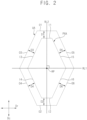
- FIG. 2 is a diagram illustrating a unit area and a pixel area included in the display device of FIG. 1 .
- a display device may include a display area DA.
- the display area DA may be an area for displaying an image.
- a portion of the display area DA is illustrated for convenience of illustration.
- the display area DA may be divided into a plurality of unit areas UA.
- the plurality of unit areas UA may be defined as a set of minimum units capable of filling the display area DA without blanking or overlapping with each other.
- Each of the plurality of unit areas UA may have the same or substantially the same shape as each other.
- the unit area UA may have a hexagonal shape in which each of all interior angles is less than 180 degrees.
- Each of the plurality of unit areas UA may have a first border defining a boundary of each of the plurality of unit areas UA.
- the first border may be an imaginary line that is not recognized by a user of the display device.
- the first border may be point-symmetric with respect to a reference point RP located within (e.g., at a center of) the unit area UA.
- the phrase "the reference point RP is located within the unit area UA” may have the same or substantially the same meaning as the phrase "the reference point RP is surrounded (e.g., around a periphery thereof) by the first border”.
- first border may be line-symmetric with respect to each of a first reference line RL1 passing (e.g., extending) through the reference point in a row direction Dr, and a second reference line RL2 passing (e.g., extending) through the reference point in a column direction Dc crossing (e.g., perpendicular to or substantially perpendicular to) the row direction Dr.
- first reference line RL1 passing (e.g., extending) through the reference point in a row direction Dr
- second reference line RL2 passing (e.g., extending) through the reference point in a column direction Dc crossing (e.g., perpendicular to or substantially perpendicular to) the row direction Dr.
- the first border may have a hexagonal shape including a first outer side O1, a second outer side O2, a third outer side O3, a fourth outer side O4, a fifth outer side O5, and a sixth outer side O6.
- a length of the first outer side O1 may be the same or substantially the same as a length of the second outer side O2, and the first outer side O1 may be parallel to or substantially parallel to the second outer side O2.
- the first outer side O1 may be parallel to or substantially parallel to the row direction Dr. Accordingly, the second outer side O2 of one unit area UA from among two unit areas UA that are adjacent to each other in the column direction Dc from among the plurality of unit areas UA may contact the first outer side O1 of the other unit area UA from among the two unit areas UA.
- the third outer side O3 and the fourth outer side O4 may connect one end of the first outer side O1 and one end of the second outer side O2 to each other.
- the fifth outer side O5 and the sixth outer side O6 may connect the other end of the first outer side O1 opposite to the one end of the first outer side O1 and the other end of the second outer side O2 opposite to the one end of the second outer side O2 to each other.
- a pixel area PXA may be disposed in each of the plurality of unit areas UA.
- the pixel area PXA may have a hexagonal shape in which a size of each of all interior angles is less than 180 degrees.
- the pixel area PXA may have a second border defining a boundary of the pixel area PXA.
- the second border may be an imaginary line that is not recognized by a user of the display device. Because the pixel area PXA is disposed in each of the plurality of unit areas UA, the second border may be disposed inside (e.g., within) the first border. In this case, the second border may be spaced apart from the first border.
- the second border may be point-symmetric with respect to the reference point RP located within (e.g., at a center of) the unit area UA (e.g., or within (e.g., at a center of) the pixel area PXA).
- the second border may be line-symmetric with respect to each of the first reference line RL1 passing (e.g., extending) through the reference point in the row direction Dr and the second reference line RL2 passing (e.g., extending) through the reference point in the column direction Dc.
- the second border may have a hexagonal shape including a first inner side I1 adjacent to the first outer side O1, a second inner side I2 adjacent to the second outer side O2, a third inner side I3 adjacent to the third outer side O3, a fourth inner side I4 adjacent to the fourth outer side O4, a fifth inner side I5 adjacent to the fifth outer side O5, and a sixth inner side I6 adjacent to the sixth outer side O6.
- the third inner side I3 and the fourth inner side I4 may connect one end of the first inner side I1 and one end of the second inner side I2 to each other.
- the fifth inner side I5 and the sixth inner side I6 may connect the other end of the first inner side I1 opposite to the one end of the first inner side I1 and the other end of the second inner side I2 opposite to the one end of the second inner side I2 to each other.
- first inner side I1 may be parallel to or substantially parallel to the first outer side O1
- second inner side I2 may be parallel to or substantially parallel to the second outer side O2
- third inner side I3 may be parallel to or substantially parallel to the third outer side O3
- fourth inner side I4 may be parallel to or substantially parallel to the fourth outer side O4
- fifth inner side I5 may be parallel to or substantially parallel to the fifth outer side O5
- sixth inner side I6 may be parallel to or substantially parallel to the sixth outer side O6.
- the first inner side I1 may be spaced apart from the first outer side O1 by a first distance D1
- the second inner side I2 may be spaced apart from the second outer side O2 by a second distance D2
- the third inner side I3 may be spaced apart from the third outer side O3 by a third distance D3
- the fourth inner side I4 may be spaced apart from the fourth outer side O4 by a fourth distance D4
- the fifth inner side I5 may be spaced apart from the fifth outer side O5 by a fifth distance D5
- the sixth inner side I6 may be spaced apart from the sixth outer side O6 by a sixth distance D6.
- the first distance D1, the second distance D2, the third distance D3, the fourth distance D4, the fifth distance D5, and the sixth distance D6 may be identical or substantially identical to each other.
- a first sub-pixel area SA1a, a second sub-pixel area SA2a, a third sub-pixel area SA3a, and a fourth sub-pixel area SA4a may be disposed in the pixel area PXA.
- Each of the first to fourth sub-pixel areas SA1a, SA2a, SA3a, and SA4a may be a minimum unit for emitting or substantially emitting light.
- each of the first to fourth sub-pixel areas SA1a, SA2a, SA3a, and SA4a may correspond to an opening of a pixel defining layer (e.g., refer to PDL of FIG. 4 ), and a light emitting material may be disposed in the opening. This will be described in more detail below with reference to FIG. 3 and FIG. 4 .
- a border of the first sub-pixel area SA1a may include the first inner side I1.
- a border of the fourth sub-pixel area SA4a may include the second inner side I2. Accordingly, in one or more embodiments of the present disclosure, the fourth sub-pixel area SA4a disposed in one unit area UA from among two unit areas UA that are adjacent to each other in the column direction Dc from among the plurality of unit areas UA may be adjacent to the first sub-pixel area SA1a of the other unit area UA from among the two unit areas UA.
- a border of the second sub-pixel area SA2a may include a portion of the second border.
- the second sub-pixel area SA2a may include a portion of the third inner side I3 adjacent to the fourth inner side I4, and a portion of the fourth inner side I4 adjacent to the third inner side I3.
- a border of the third sub-pixel area SA3a may include another portion of the second border.
- the third sub-pixel area SA3a may include a portion of the fifth inner side I5 adjacent to the sixth inner side I6, and a portion of the sixth inner side I6 adjacent to the fifth inner side I5.
- Unit areas UA arranged in the column direction Dc from among the plurality of unit areas UA may define a plurality of pixel columns.
- the plurality of pixel columns may include a first pixel column C1, and a second pixel column C2 adjacent to the first pixel column C1 in the row direction Dr.
- the second pixel column C2 may be a pixel column in which the first pixel column C1 is shifted by a suitable distance (e.g., a predetermined distance) in the column direction Dc.
- the plurality of pixel columns may be interlocked with one another, and arranged along the row direction Dr.
- the first pixel column C1 and the second pixel column C2 may be interlocked with each other, and alternately arranged along the row direction Dr.
- FIG. 3 is a plan view illustrating a sub-pixel area according to a first embodiment.
- FIG. 4 is a cross-sectional view taken along the line I-I' of FIG. 3 .
- the unit area UA, the pixel area PXA, and the first to fourth sub-pixel areas SA1a, SA2a, SA3a, and SA4a illustrated in FIG. 3 may be the same or substantially the same as the unit area UA, the pixel area PXA, and the first to fourth sub-pixel areas SA1a, SA2a, SA3a, and SA4a described above with reference to FIG. 1 and FIG. 2 , and thus, redundant description thereof may not be repeated.
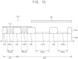
- the display device may include a substrate SUB, first to fourth pixel electrodes PXE1, PXE2, PXE3, and PXE4, a pixel defining layer PDL, and first to third light emitting materials EL1, EL2, and EL3.
- the substrate SUB may include a plurality of insulation layers, and a plurality of transistors.
- the substrate SUB may include a material having flexibility, so as to be repeatedly folded and/or unfolded.
- the first to fourth pixel electrodes PXE1, PXE2, PXE3, and PXE4 may be disposed on the substrate SUB.
- the first to fourth pixel electrodes PXE1, PXE2, PXE3, and PXE4 may be disposed to be spaced apart from each other.
- the first to fourth pixel electrodes PXE1, PXE2, PXE3, and PXE4 may be disposed in the unit area UA.
- Each of the first to fourth pixel electrodes PXE1, PXE2, PXE3, and PXE4 may be electrically connected to the plurality of transistors.
- each of the first to fourth pixel electrodes PXE1, PXE2, PXE3, and PXE4 may be referred to as an anode electrode.
- the pixel defining layer PDL may be disposed on the first to fourth pixel electrodes PXE1, PXE2, PXE3, and PXE4.
- the pixel defining layer PDL may include an organic material.
- the pixel defining layer PDL may define an opening exposing each of the first to fourth pixel electrodes PXE1, PXE2, PXE3, and PXE4.
- the opening may include a first pixel opening exposing the first pixel electrode PXE1, a second pixel opening exposing the second pixel electrode PXE2, a third pixel opening exposing the third pixel electrode PXE3, and a fourth pixel opening exposing the fourth pixel electrode PXE4.
- the first to third light emitting materials EL1, EL2, and EL3 may include a suitable material for emitting light.
- the first to third light emitting materials EL1, EL2, and EL3 may include an organic light emitting material.
- the first to third light emitting materials EL1, EL2, and EL3 may be disposed in the opening.
- the first light emitting material EL1 may be disposed in the first pixel opening and the fourth pixel opening
- the second light emitting material EL2 may be disposed in the second pixel opening
- the third light emitting material EL3 may be disposed in the third pixel opening.
- the first to third light emitting materials EL1, EL2, and EL3 may be further disposed on the pixel defining layer PDL.
- an area in which the first light emitting material EL1 may be located may be a first area A1a and a fourth area A4a
- an area in which the second light emitting material EL2 may be located may be a second area A2a
- an area in which the third light emitting material EL3 may be located may be a third area A3a.
- the first to fourth areas A1a, A2a, A3a, and A4a may be disposed in the unit area UA.
- an entire outer border of the first to fourth areas A1a, A2a, A3a, and A4a may be the same or substantially the same as the first border of the unit area UA.
- the first light emitting material EL1 may emit light having a first color
- the second light emitting material EL2 may emit light having a second color
- the third light emitting material EL3 may emit light having a third color.
- the light of the first color may have a peak wavelength in a range of about 510 nm or more and about 550 nm or less
- the light of the second color may have a peak wavelength in a range of about 610 nm or more and about 650 nm or less
- the light of the third color may have a peak wavelength in a range of about 440 nm or more and about 480 nm or less.
- the first color may be green
- the second color may be red
- the third color may be blue.
- a common electrode covering the first to third light emitting materials EL1, EL2, and EL3 may be disposed on the pixel defining layer PDL.
- the common electrode may include a transparent conductive material.
- the common electrode may be referred to as a cathode electrode.
- the first sub-pixel area SA1a may be defined as an area corresponding to the first pixel opening.
- the first sub-pixel area SA1a may be an area in which light is emitted or substantially emitted from the first light emitting material EL1 among the first area A1a.
- the first sub-pixel area SA1a may have a pentagonal shape.
- a border of the first sub-pixel area SA1a may include the first inner side I1, a portion of the third inner side I3 adjacent to the first inner side I1, and a portion of the fifth inner side I5 adjacent to the first inner side I1.
- the first area A1a may have a pentagonal shape.
- a border of the first area A1a may surround (e.g., around a periphery of) the border of the first sub-pixel area SA1a.
- the second sub-pixel area SA2a may be defined as an area corresponding to the second pixel opening.
- the second sub-pixel area SA2a may be an area in which light is emitted or substantially emitted from the second light emitting material EL2 among the second area A2a.
- the second sub-pixel area SA2a may have a pentagonal shape.
- a border of the second sub-pixel area SA2a may include a portion of the third inner side I3 adjacent to the fourth inner side I4, and a portion of the fourth inner side I4 adjacent to the third inner side I3.
- the second area A2a may have a pentagonal shape.
- a border of the second area A2a may surround (e.g., around a periphery of) the border of the second sub-pixel area SA2a.
- the third sub-pixel area SA3a may be defined as an area corresponding to the third pixel opening.
- the third sub-pixel area SA3a may be an area in which light is emitted or substantially emitted from the third light emitting material EL3 among the third area A3a.
- the third sub-pixel area SA3a may have a pentagonal shape.
- a border of the third sub-pixel area SA3a may include a portion of the fifth inner side I5 adjacent to the sixth inner side I6, and a portion of the sixth inner side I6 adjacent to the fifth inner side I5.
- the third area A3a may have a pentagonal shape.
- a border of the third area A3a may surround (e.g., around a periphery of) the third sub-pixel area SA3a.
- the fourth sub-pixel area SA4a may be defined as an area corresponding to the fourth pixel opening.
- the fourth sub-pixel area SA4a may be an area in which light is emitted or substantially emitted from the first light emitting material EL1 among the fourth area A4a.
- the fourth sub-pixel area SA4a may have a pentagonal shape.
- a border of the fourth sub-pixel area SA4a may include the second inner side I2, a portion of the fourth inner side I4 adjacent to the second inner side I2, and a portion of the sixth inner side I6 adjacent to the second inner side I2.
- the border of the fourth sub-pixel area SA4a and the border of the first sub-pixel area SA1a may be line-symmetric with each other with respect to the first reference line RL1 described above with reference to FIG. 2 .
- the fourth area A4a may have a pentagonal shape.
- a border of the fourth area SA4a may surround (e.g., around a periphery of) the fourth sub-pixel area SA4a.
- each of the first to fourth sub-pixel areas SA1a, SA2a, SA3a, and SA4a may have various suitable areas.
- an area of the first sub-pixel area SA1a may be the same or substantially the same as an area of the fourth sub-pixel area SA4a.
- an area of the second sub-pixel area SA2a may be different from an area of the third sub-pixel area SA3a.
- the area of the third sub-pixel area SA3a may be larger than the area of the second sub-pixel area SA2a.
- the area of the third sub-pixel area SA3a may be smaller than the area of the second sub-pixel area SA2a.
- the area of the first sub-pixel area SA1a may be smaller than the area of the second sub-pixel area SA2a, and may be smaller than the area of the third sub-pixel area SA3a.
- the area of the fourth sub-pixel area SA4a may be smaller than the area of the second sub-pixel area SA2a, and may be smaller than the area of the third sub-pixel area SA3a.
- FIG. 5 is a plan view illustrating a sub-pixel area according to a second embodiment.
- the unit area UA and the pixel area PXA illustrated in FIG. 5 may be the same or substantially same as (or similar to) the unit area UA and the pixel area PXA described above with reference to FIG. 1 and FIG. 2 , and thus, redundant description thereof may not be repeated.
- first to fourth sub-pixel areas SA1b, SA2b, SA3b, and SA4b according to the second embodiment may be the same or substantially the same as (or similar to) the first to fourth sub-pixel areas SA1a, SA2a, SA3a, and SA4a described above with reference to FIG. 3 and FIG. 4 , except for a planar shape thereof.
- first to fourth areas A1b, A2b, A3b, and A4b according to the second embodiment may be the same or substantially same as the first to fourth areas A1a, A2a, A3a, and A4a described above with reference to FIG. 3 and FIG. 4 , except for a planar shape thereof. Accordingly, redundant description thereof may not be repeated, and the differences therebetween may be mainly described hereinafter.
- the first sub-pixel area SA1b may have a pentagonal shape.
- a border of the first sub-pixel area SA1b may include the first inner side I1, a portion of the third inner side I3 adjacent to the first inner side I1, and a portion of the fifth inner side I5 adjacent to the first inner side I1.
- the first area A1b may have a pentagonal shape.
- a border of the first area A1b may surround (e.g., around a periphery of) the border of the first sub-pixel area SA1b.
- the second sub-pixel area SA2b may have a quadrangular shape.
- a border of the second sub-pixel area SA2b may include a portion of the third inner side I3 adjacent to the fourth inner side I4, and a portion of the fourth inner side I4 adjacent to the third inner side I3.
- the second area A2b may have a quadrangular shape.
- a border of the second area A2b may surround (e.g., around a periphery of) the border of the second sub-pixel area SA2b.
- the third sub-pixel area SA3b may have a quadrangular shape.
- a border of the third sub-pixel area SA3b may include a portion of the fifth inner side I5 adjacent to the sixth inner side I6, and a portion of the sixth inner side I6 adjacent to the fifth inner side I5.
- the third area A3b may have a quadrangular shape.
- a border of the third area A3b may surround (e.g., around a periphery of) the border of the third sub-pixel area SA3a.
- the fourth sub-pixel area SA4b may have a pentagonal shape.
- a border of the fourth sub-pixel area SA4b may include the second inner side I2, a portion of the fourth inner side I4 adjacent to the second inner side I2, and a portion of the sixth inner side I6 adjacent to the second inner side I2.
- the border of the fourth sub-pixel area SA4b and the border of the first sub-pixel area SA1b may be line-symmetric with each other with respect to the first reference line RL1 described above with reference to FIG. 2 .
- the fourth area SA4b may have a pentagonal shape.
- a border of the fourth area A4b may surround (e.g., around a periphery of) the border of the fourth sub-pixel area SA4b.
- Each of the first to fourth sub-pixel areas SA1b, SA2b, SA3b, and SA4b may have various suitable areas.
- an area of the first sub-pixel area SA1b may be the same or substantially the same as an area of the fourth sub-pixel area SA4b.
- an area of the second sub-pixel area SA2b may be different from an area of the third sub-pixel area SA3b.
- the area of the third sub-pixel area SA3b may be larger than the area of the second sub-pixel area SA2b.
- the area of the third sub-pixel area SA3b may be smaller than the area of the second sub-pixel area SA2b.
- the area of the first sub-pixel area SA1b may be smaller than the area of the second sub-pixel area SA2b, and may be smaller than the area of the third sub-pixel area SA3b.
- the area of the fourth sub-pixel area SA4b may be smaller than the area of the second sub-pixel area SA2b, and may be smaller than the area of the third sub-pixel area SA3b.
- FIG. 6 is a plan view illustrating a sub-pixel area according to a third embodiment.
- the unit area UA and the pixel area PXA illustrated in FIG. 6 may be the same or substantially the same as the unit area UA and the pixel area PXA described above with reference to FIG. 1 and FIG. 2 , and thus, redundant description thereof may not be repeated.
- first to fourth sub-pixel areas SA1c, SA2c, SA3c, and SA4c according to the third embodiment may be the same or substantially the same as the first to fourth sub-pixel areas SA1a, SA2a, SA3a, and SA4a described above with reference to FIG. 3 and FIG. 4 , except for a planar shape thereof.
- first to fourth areas A1c, A2c, A3c, and A4c according to the third embodiment may be the same or substantially the same as the first to fourth areas A1a, A2a, A3a, and A4a described above with reference to FIG. 3 and FIG. 4 , except for a planar shape thereof. Accordingly, redundant description thereof may not be repeated, and the differences therebetween may be mainly described hereinafter.
- the first sub-pixel area SA1c may have a quadrangular shape.
- a border of the first sub-pixel area SA1c may include the first inner side I1, a portion of the third inner side I3 adjacent to the first inner side I1, and a portion of the fifth inner side I5 adjacent to the first inner side I1.
- the first area A1c may have a quadrangular shape.
- a border of the first area A1c may surround (e.g., around a periphery of) the border of the first sub-pixel area SA1c.
- the second sub-pixel area SA2c may have a pentagonal shape.
- a border of the second sub-pixel area SA2c may include a portion of the third inner side I3 adjacent to the fourth inner side I4, and a portion of the fourth inner side I4 adjacent to the third inner side I3.
- the second area A2c may have a pentagonal shape.
- a border of the second area A2c may surround (e.g., around a periphery of) the border of the second sub-pixel area SA2c.
- the third sub-pixel area SA3c may have a pentagonal shape.
- a border of the third sub-pixel area SA3c may include a portion of the fifth inner side I5 adjacent to the sixth inner side I6 and a portion of the sixth inner side I6 adjacent to the fifth inner side I5.
- the third area A3c may have a pentagonal shape.
- a border of the third area A3c may surround (e.g., around a periphery of) the third sub-pixel area SA3c.
- the fourth sub-pixel area SA4c may have a quadrangular shape.
- a border of the fourth sub-pixel area SA4c may include the second inner side I2, a portion of the fourth inner side I4 adjacent to the second inner side I2, and a portion of the sixth inner side I6 adjacent to the second inner side I2.
- the border of the fourth sub-pixel area SA4c and the border of the first sub-pixel area SA1c may be line-symmetric with each other with respect to the first reference line RL1 described above with reference to FIG. 2 .
- each of the border of the fourth sub-pixel area SA4c and the border of the first sub-pixel area SA1c may be line-symmetric with each other with respect to the second reference line RL2 described above with reference to FIG. 2 .
- the fourth area A4c may have a quadrangular shape.
- a border of the fourth area A4c may surround (e.g., around a periphery of) the border of the fourth sub-pixel area SA4c.
- Each of the first to fourth sub-pixel areas SA1c, SA2c, SA3c, and SA4c may have various suitable areas.
- an area of the first sub-pixel area SA1c may be the same or substantially the same as an area of the fourth sub-pixel area SA4c.
- an area of the second sub-pixel area SA2c may be different from an area of the third sub-pixel area SA3c.
- the area of the third sub-pixel area SA3c may be larger than the area of the second sub-pixel area SA2c.
- the area of the third sub-pixel area SA3c may be smaller than the area of the second sub-pixel area SA2c.
- the area of the first sub-pixel area SA1c may be smaller than the area of the second sub-pixel area SA2c, and may be smaller than the area of the third sub-pixel area SA3c.
- the area of the fourth sub-pixel area SA4c may be smaller than the area of the second sub-pixel area SA2c, and may be smaller than the area of the third sub-pixel area SA3c.
- FIG. 7 is a plan view illustrating a sub-pixel area according to a fourth embodiment.
- the unit area UA and the pixel area PXA illustrated in FIG. 7 may be the same or substantially the same as the unit area UA and the pixel area PXA described above with reference to FIG. 1 and FIG. 2 , and thus, redundant description thereof may not be repeated.
- first to fourth sub-pixel areas SA1d, SA2d, SA3d, and SA4d according to the fourth embodiment may be the same or substantially same as the first to fourth sub-pixel areas SA1a, SA2a, SA3a, and SA4a described above with reference to FIG. 3 and FIG. 4 , except for a planar shape thereof.
- first to fourth areas A1d, A2d, A3d, and A4d according to the fourth embodiment may be the same or substantially the same as the first to fourth areas A1a, A2a, A3a, and A4a described above with reference to FIG. 3 and FIG. 4 , except for a planar shape thereof. Accordingly, redundant description thereof may not be repeated, and the differences therebetween may be mainly described hereinafter.
- the first sub-pixel area SA1d may have a quadrangular shape.
- a border of the first sub-pixel area SA1d may include the first inner side I1, a portion of the third inner side I3 adjacent to the first inner side I1, and a portion of the fifth inner side I5 adjacent to the first inner side I1.
- the first area A1d may have a quadrangular shape.
- a border of the first area A1d may surround (e.g., around a periphery of) the border of the first sub-pixel area SA1d.
- the second sub-pixel area SA2d may have a quadrangular shape.
- a border of the second sub-pixel area SA2d may include a portion of the third inner side I3 adjacent to the fourth inner side I4, and a portion of the fourth inner side I4 adjacent to the third inner side I3.
- the second area A2d may have a pentagonal shape.
- a border of the second area A2c may surround (e.g., around a periphery of) the border of the second sub-pixel area SA2c.
- the third sub-pixel area SA3d may have a quadrangular shape.
- a border of the third sub-pixel area SA3d may include a portion of the fifth inner side I5 adjacent to the sixth inner side I6, and a portion of the sixth inner side I6 adjacent to the fifth inner side I5.
- the third area A3d may have a pentagonal shape.
- a border of the third area A3d may surround (e.g., around a periphery of) the third sub-pixel area SA3d.
- the fourth sub-pixel area SA4d may have a quadrangular shape.
- a border of the fourth sub-pixel area SA4d may include the second inner side I2, a portion of the fourth inner side I4 adjacent to the second inner side I2, and a portion of the sixth inner side I6 adjacent to the second inner side I2.
- the border of the fourth sub-pixel area SA4d and the border of the first sub-pixel area SA1d may be line-symmetric with each other with respect to the first reference line RL1 described above with reference to FIG. 2 .
- each of the border of the fourth sub-pixel area SA4d and the border of the first sub-pixel area SA1d may be line-symmetric with each other with respect to the second reference line RL2 described above with reference to FIG. 2 .
- the fourth area A4d may have a quadrangular shape.
- a border of the fourth area A4d may surround (e.g., around a periphery of) the border of the fourth sub-pixel area SA4d.
- Each of the first to fourth sub-pixel areas SA1d, SA2d, SA3d, and SA4d may have various suitable areas.
- an area of the first sub-pixel area SA1d may be the same or substantially the same as an area of the fourth sub-pixel area SA4d.
- an area of the second sub-pixel area SA2d may be different from an area of the third sub-pixel area SA3d.
- the area of the third sub-pixel area SA3d may be larger than the area of the second sub-pixel area SA2d.
- the area of the third sub-pixel area SA3d may be smaller than the area of the second sub-pixel area SA2d.
- the area of the first sub-pixel area SA1d may be smaller than the area of the second sub-pixel area SA2d, and may be smaller than the area of the third sub-pixel area SA3d.
- the area of the fourth sub-pixel area SA4d may be smaller than the area of the second sub-pixel area SA2d, and may be smaller than the area of the third sub-pixel area SA3d.
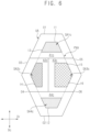
- FIG. 8 is a plan view illustrating a sub-pixel area according to a fifth embodiment.
- the unit area UA and the pixel area PXA illustrated in FIG. 8 may be the same or substantially the same as the unit area UA and the pixel area PXA described above with reference to FIG. 1 and FIG. 2 , and thus, redundant description thereof may not be repeated.
- first to fourth sub-pixel areas SA1e, SA2e, SA3e, and SA4e according to the fifth embodiment may be the same or substantially the same as the first to fourth sub-pixel areas SA1a, SA2a, SA3a, and SA4a described above with reference to FIG. 3 and FIG. 4 , except for a planar shape thereof.
- first to fourth areas A1e, A2e, A3e, and A4e according to the fifth embodiment may be the same or substantially same as the first to fourth areas A1a, A2a, A3a, and A4a described above with reference to FIG. 3 and FIG. 4 , except for a planar shape thereof. Accordingly, redundant description thereof may not be repeated, and the differences therebetween may be mainly described hereinafter.
- the first sub-pixel area SA1e may have a quadrangular shape.
- a border of the first sub-pixel area SA1e may include the first inner side I1, and a portion of the fifth inner side I5 adjacent to the first inner side I1.
- the first area A1e may have a pentagonal shape.
- a border of the first area A1e may surround (e.g., around a periphery of) the border of the first sub-pixel area SA1e.
- the second sub-pixel area SA2e may have a pentagonal shape.
- a border of the second sub-pixel area SA2e may include a portion of the third inner side I3 adjacent to the fourth inner side I4, and a portion of the fourth inner side I4 adjacent to the third inner side I3.
- the second area A2e may have a pentagonal shape.
- a border of the second area A2e may surround (e.g., around a periphery of) the border of the second sub-pixel area SA2e.
- the third sub-pixel area SA3e may have a pentagonal shape.
- a border of the third sub-pixel area SA3e may include a portion of the fifth inner side I5 adjacent to the sixth inner side I6, and a portion of the sixth inner side I6 adjacent to the fifth inner side I5.
- the third area A3e may have a pentagonal shape.
- a border of the third area A3e may surround (e.g., around a periphery of) the third sub-pixel area SA3e.
- the fourth sub-pixel area SA4e may have a quadrangular shape.
- a border of the fourth sub-pixel area SA4e may include the second inner side I2, and a portion of the sixth inner side I6 adjacent to the second inner side I2.
- the border of the fourth sub-pixel area SA4e and the border of the first sub-pixel area SA1e may be line-symmetric with each other with respect to the first reference line RL1 described above with reference to FIG. 2 .
- the fourth area A4d may have a pentagonal shape.
- a border of the fourth area A4e may surround (e.g., around a periphery of) the border of the fourth sub-pixel area SA4e.
- Each of the first to fourth sub-pixel areas SA1e, SA2e, SA3e, and SA4e may have various suitable areas.
- an area of the first sub-pixel area SA1e may be the same or substantially the same as an area of the fourth sub-pixel area SA4e.
- an area of the second sub-pixel area SA2e may be different from an area of the third sub-pixel area SA3e.
- the area of the third sub-pixel area SA3e may be larger than the area of the second sub-pixel area SA2e.
- the area of the third sub-pixel area SA3e may be smaller than the area of the second sub-pixel area SA2e.
- the area of the first sub-pixel area SA1e may be smaller than the area of the second sub-pixel area SA2e, and may be smaller than the area of the third sub-pixel area SA3e.
- the area of the fourth sub-pixel area SA4e may be smaller than the area of the second sub-pixel area SA2e, and may be smaller than the area of the third sub-pixel area SA3e.
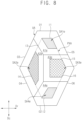
- FIG. 9 is a plan view illustrating a sub-pixel area according to a sixth embodiment.
- the unit area UA and the pixel area PXA illustrated in FIG. 9 may be the same or substantially the same as the unit area UA and the pixel area PXA described above with reference to FIG. 1 and FIG. 2 , and thus, redundant description thereof may not be repeated.
- first to fourth sub-pixel areas SA1f, SA2f, SA3f, and SA4f according to the sixth embodiment may be the same or substantially the same as the first to fourth sub-pixel areas SA1a, SA2a, SA3a, and SA4a described above with reference to FIG. 3 and FIG. 4 , except for a planar shape thereof.
- first to fourth areas A1f, A2f, A3f, and A4f according to the sixth embodiment may be the same or substantially the same as the first to fourth areas A1a, A2a, A3a, and A4a described above with reference to FIG. 3 and FIG. 4 , except for a planar shape thereof. Accordingly, redundant description thereof may not be repeated, and the differences therebetween may be mainly described hereinafter.
- the first sub-pixel area SA1f may have a hexagonal shape.
- a border of the first sub-pixel area SA1f may include the first inner side I1, a portion of the third inner side I3 adjacent to the first inner side I1, and a portion of the fifth inner side I5 adjacent to the first inner side I1.
- the first area A1f may have a pentagonal shape.
- a border of the first area A1f may surround (e.g., around a periphery of) the border of the first sub-pixel area SA1f.
- the second sub-pixel area SA2f may have a pentagonal shape.
- a border of the second sub-pixel area SA2f may include a portion of the third inner side I3 adjacent to the fourth inner side I4, and a portion of the fourth inner side I4 adjacent to the third inner side I3.
- the second area A2f may have a pentagonal shape.
- a border of the second area A2f may surround (e.g., around a periphery of) the border of the second sub-pixel area SA2f.
- the third sub-pixel area SA3f may have a pentagonal shape.
- a border of the third sub-pixel area SA3f may include a portion of the fifth inner side I5 adjacent to the sixth inner side I6, and a portion of the sixth inner side I6 adjacent to the fifth inner side I5.
- the third area A3f may have a pentagonal shape.
- a border of the third area A3f may surround (e.g., around a periphery of) the third sub-pixel area SA3f.
- the fourth sub-pixel area SA4f may have a hexagonal shape.
- a border of the fourth sub-pixel area SA4f may include the second inner side I2, a portion of the fourth inner side I4 adjacent to the second inner side I2, and a portion of the sixth inner side I6 adjacent to the second inner side I2.
- the border of the fourth sub-pixel area SA4f and the border of the first sub-pixel area SA1f may be line-symmetric with each other with respect to the first reference line RL1 described above with reference to FIG. 2 .
- the fourth area A4f may have a pentagonal shape.
- a border of the fourth area A4f may surround (e.g., around a periphery of) the border of the fourth sub-pixel area SA4f.
- Each of the first to fourth sub-pixel areas SA1f, SA2f, SA3f, and SA4f may have various suitable areas.
- an area of the first sub-pixel area SA1f may be the same or substantially the same as an area of the fourth sub-pixel area SA4f.
- an area of the second sub-pixel area SA2f may be different from an area of the third sub-pixel area SA3f.
- the area of the third sub-pixel area SA3f may be larger than the area of the second sub-pixel area SA2f.
- the area of the third sub-pixel area SA3f may be smaller than the area of the second sub-pixel area SA2f.
- the area of the first sub-pixel area SA1f may be smaller than the area of the second sub-pixel area SA2f, and may be smaller than the area of the third sub-pixel area SA3f.
- the area of the fourth sub-pixel area SA4f may be smaller than the area of the second sub-pixel area SA2f, and may be smaller than the area of the third sub-pixel area SA3f.
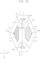
- FIG. 10 is a plan view illustrating a sub-pixel area according to a seventh embodiment.
- the unit area UA and the pixel area PXA illustrated in FIG. 10 may be the same or substantially the same as the unit area UA and the pixel area PXA described above with reference to FIG. 1 and FIG. 2 , and thus, redundant description thereof may not be repeated.
- first to fourth sub-pixel areas SA1g, SA2g, SA3g, and SA4g according to the seventh embodiment may be the same or substantially the same as the first to fourth sub-pixel areas SA1a, SA2a, SA3a, and SA4a described above with reference to FIG. 3 and FIG. 4 , except for a planar shape thereof.
- first to fourth areas A1g, A2g, A3g, and A4g according to the seventh embodiment may be the same or substantially the same as the first to fourth areas A1a, A2a, A3a, and A4a described above with reference to FIG. 3 and FIG. 4 , except for a planar shape thereof. Accordingly, redundant description thereof may not be repeated, and the differences therebetween may be mainly described hereinafter.
- the first sub-pixel area SA1g may have a triangle shape.
- a border of the first sub-pixel area SA1g may include the first inner side I1.
- the first area A1g may have a pentagonal shape.
- a border of the first area A1g may surround (e.g., around a periphery of) the border of the first sub-pixel area SA1g.
- the second sub-pixel area SA2g may have a pentagonal shape.
- a border of the second sub-pixel area SA2g may include a portion of the third inner side I3 adjacent to the fourth inner side I4, and a portion of the fourth inner side I4 adjacent to the third inner side I3.
- the second area A2g may have a pentagonal shape.
- a border of the second area A2g may surround (e.g., around a periphery of) the border of the second sub-pixel area SA2g.
- the third sub-pixel area SA3g may have a pentagonal shape.
- a border of the third sub-pixel area SA3g may include a portion of the fifth inner side I5 adjacent to the sixth inner side I6, and a portion of the sixth inner side I6 adjacent to the fifth inner side I5.
- the third area A3g may have a pentagonal shape.
- a border of the third area A3g may surround (e.g., around a periphery of) the third sub-pixel area SA3g.
- the fourth sub-pixel area SA4g may have a triangle shape.
- a border of the fourth sub-pixel area SA4g may include the second inner side I2.
- the border of the fourth sub-pixel area SA4g and the border of the first sub-pixel area SA1g may be line-symmetric with each other with respect to the first reference line RL1 described above with reference to FIG. 2 .
- the fourth area A4g may have a pentagonal shape.
- a border of the fourth area A4g may surround (e.g., around a periphery of) the border of the fourth sub-pixel area SA4g.
- Each of the first to fourth sub-pixel areas SA1g, SA2g, SA3g, and SA4g may have various suitable areas.
- an area of the first sub-pixel area SA1g may be the same or substantially the same as an area of the fourth sub-pixel area SA4g.
- an area of the second sub-pixel area SA2g may be different from an area of the third sub-pixel area SA3g.
- the area of the third sub-pixel area SA3g may be larger than the area of the second sub-pixel area SA2g.
- the area of the third sub-pixel area SA3g may be smaller than the area of the second sub-pixel area SA2g.
- the area of the first sub-pixel area SA1g may be smaller than the area of the second sub-pixel area SA2g, and may be smaller than the area of the third sub-pixel area SA3g.
- the area of the fourth sub-pixel area SA4g may be smaller than the area of the second sub-pixel area SA2g, and may be smaller than the area of the third sub-pixel area SA3g.
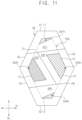
- FIG. 11 is a plan view illustrating a sub-pixel area according to an eighth embodiment.
- the unit area UA and the pixel area PXA illustrated in FIG. 11 may be the same or substantially the same as the unit area UA and the pixel area PXA described above with reference to FIG. 1 and FIG. 2 , and thus, redundant description thereof may not be repeated.
- first to fourth sub-pixel areas SA1h, SA2h, SA3h, and SA4h according to the eighth embodiment may be the same or substantially the same as the first to fourth sub-pixel areas SA1a, SA2a, SA3a, and SA4a described above with reference to FIG. 3 and FIG. 4 , except for a planar shape thereof.
- first to fourth areas A1h, A2h, A3h, and A4h according to the eighth embodiment may be the same or substantially the same as the first to fourth areas A1a, A2a, A3a, and A4a described above with reference to FIG. 3 and FIG. 4 , except for a planar shape thereof. Accordingly, redundant description thereof may not be repeated, and the differences therebetween may be mainly described hereinafter.
- the first sub-pixel area SA1h may have a triangle shape.
- a border of the first sub-pixel area SA1h may include the first inner side I1, and a portion of the third inner side I3 adjacent to the first inner side I1.
- the first area A1h may have a quadrangular shape.
- a border of the first area A1h may surround (e.g., around a periphery of) the border of the first sub-pixel area SA1h.
- the second sub-pixel area SA2h may have a quadrangular shape.
- a border of the second sub-pixel area SA2h may include a portion of the third inner side I3 adjacent to the fourth inner side I4, and a portion of the fourth inner side I4 adjacent to the third inner side I3.
- the second area A2h may have a pentagonal shape.
- a border of the second area A2h may surround (e.g., around a periphery of) the border of the second sub-pixel area SA2h.
- the third sub-pixel area SA3h may have a quadrangular shape.
- a border of the third sub-pixel area SA3h may include a portion of the fifth inner side I5 adjacent to the sixth inner side I6, and a portion of the sixth inner side I6 adjacent to the fifth inner side I5.
- the third area A3h may have a pentagonal shape.
- a border of the third area A3h may surround (e.g., around a periphery of) the third sub-pixel area SA3h.
- the fourth sub-pixel area SA4h may have a triangle shape.
- a border of the fourth sub-pixel area SA4h may include the second inner side I2, and a portion of the sixth inner side I6 adjacent to the second inner side I2.
- the border of the fourth sub-pixel area SA4h and the border of the first sub-pixel area SA1h may be point-symmetric with each other with respect to the reference point RP described above with reference to FIG. 2 .
- the fourth area A4h may have a quadrangular shape.
- a border of the fourth area A4h may surround (e.g., around a periphery of) the border of the fourth sub-pixel area SA4h.
- Each of the first to fourth sub-pixel areas SA1h, SA2h, SA3h, and SA4h may have various suitable areas.
- an area of the first sub-pixel area SA1h may be the same or substantially the same as an area of the fourth sub-pixel area SA4h.
- an area of the second sub-pixel area SA2h may be different from an area of the third sub-pixel area SA3h.
- the area of the third sub-pixel area SA3h may be larger than the area of the second sub-pixel area SA2h.
- the area of the third sub-pixel area SA3h may be smaller than the area of the second sub-pixel area SA2h.
- the area of the first sub-pixel area SA1h may be smaller than the area of the second sub-pixel area SA2h, and may be smaller than the area of the third sub-pixel area SA3h.
- the area of the fourth sub-pixel area SA4h may be smaller than the area of the second sub-pixel area SA2h, and may be smaller than the area of the third sub-pixel area SA3h.
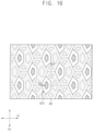
- FIG. 12 through FIG. 19 are diagrams illustrating a method of manufacturing the display device of FIG. 1 .
- a portion of the display area DA is illustrated in FIG. 12 , and redundant description as those of the embodiments described above with reference to FIG. 1 , FIG. 2 , FIG. 3 , and FIG. 4 may not be repeated.
- the pixel defining layer PDL may be formed.
- the pixel defining layer PDL may define the opening exposing each of the pixel electrodes PXE1, PXE2, PXE3, and PXE4.
- the pixel defining layer PDL may include a plurality of unit areas UA, and a pixel area disposed in each of the plurality of unit areas UA.
- the plurality of unit areas UA may include a first unit area UA1, and a second unit area UA2 adjacent to the first unit area UA1 in the column direction Dc.
- the second outer side O2 of the first unit area UA1 may be in contact with the first outer side O1 of the second unit area UA2.
- a first pixel area PXA1 may be disposed in the first unit area UA1, and a second pixel area PXA2 may be disposed in the second unit area UA2.
- the opening may include the first pixel opening exposing the first pixel electrode PXE1, the second pixel opening exposing the second pixel electrode PXE2, the third pixel opening exposing the third pixel electrode PXE3, and the fourth pixel opening exposing the fourth pixel electrode PXE4.
- the first pixel opening may correspond to the first sub-pixel area SA1a
- the second pixel opening may correspond to the second sub-pixel area SA2a
- the third pixel opening may correspond to the third sub-pixel area SA3a
- the fourth pixel opening may correspond to the fourth sub-pixel area SA4a.
- the first light emitting material EL1 may be deposited in the first pixel opening and the fourth pixel opening. In this case, the first light emitting material EL1 may be concurrently (e.g., simultaneously) deposited in the first pixel opening disposed in the second unit area UA2 and the fourth pixel opening disposed in the first unit area UA1.
- a first mask M1 may be disposed on the pixel defining layer PDL.
- the first mask M1 may define a first opening pattern OP1.
- the first opening pattern OP1 may expose the first and fourth sub-pixel areas SA1a and SA4a disposed in each of the plurality of unit areas UA.
- the first opening pattern OP1 may concurrently (e.g., simultaneously) expose the fourth sub-pixel area SA4a disposed in one of two unit areas UA that are adjacent to each other in the column direction Dc from among the plurality of unit areas UA and the first sub-pixel area SA1a disposed in the other of the two unit areas UA.
- the first opening pattern OP1 may concurrently (e.g., simultaneously) expose the fourth sub-pixel area SA4a disposed in the first unit area UA1 and the first sub-pixel area SA1a disposed in the second unit area UA2.
- the first light emitting material EL1 may be deposited on a portion exposed by the first opening pattern OP1.
- a border of the first opening pattern OP1 concurrently (e.g., simultaneously) exposing the fourth sub-pixel area SA4a disposed in the first unit area UA1 and the first sub-pixel area SA1a disposed in the second unit area UA2 may be the same or substantially the same as an overall border of the fourth area A4a disposed in the first unit area UA1 and the first area A1a (e.g., refer to FIG. 4 ) disposed in the second unit area UA2.
- the second light emitting material EL2 may be deposited in the second pixel opening.
- a second mask M2 may be disposed on the pixel defining layer PDL.
- the second mask M2 may define a second opening pattern OP2.
- the second opening pattern OP2 may expose the second sub-pixel area SA2a disposed in each of the plurality of unit areas UA.
- the second light emitting material EL2 may be deposited on a portion exposed by the second opening pattern OP2.
- a border of the second opening pattern OP2 may be the same or substantially the same as the border of the second area A2a (e.g., refer to FIG. 4 ).
- the third light emitting material EL3 may be deposited in the third pixel opening.
- a third mask M3 may be disposed on the pixel defining layer PDL.
- the third mask M3 may define a third opening pattern OP3.
- the third opening pattern OP3 may expose the third sub-pixel area SA3a disposed in each of the plurality of unit areas UA.
- the third light emitting material EL3 may be deposited on a portion exposed by the third opening pattern OP3.
- a border of the third opening pattern OP3 may be the same or substantially the same as the border of the third area A3a (e.g., refer to FIG. 4 ).
- the order of the deposition of the first to third light emitting materials EL1, EL2, and EL3 is not limited thereto.
- the third light emitting material EL3 may be deposited, and then the first light emitting material EL1 may be finally deposited.
- the second light emitting material EL2 is deposited, the first light emitting material EL1 may be deposited, and then the third light emitting material EL3 may be finally deposited.
- an area of the first opening pattern OP1 may be greater than or equal to about 80%, and less than or equal to about 120%, of an area of the third opening pattern OP3, and an area of the second opening pattern OP2 may be greater than or equal to about 80%, and less than or equal to about 120%, of the area of the third opening pattern OP3. Accordingly, an opening ratio of each of the first to third opening patterns OP1, OP2, and OP3 may be sufficiently secured, and a manufacturing yield of the first to third masks M1, M2, and M3 may be sufficiently secured.
- the border of the unit area UA may surround (e.g., around a periphery of) the border of the pixel area PXA, and the border of the unit area UA may be spaced apart from the border of the pixel area PXA.
- the pixel area PXA disposed in one of two adjacent unit areas UA and the pixel area PXA disposed in the other of the two adjacent unit areas UA may be spaced apart from each other.
- the first to third light emitting materials EL1, EL2, and EL3 are deposited, even if an alignment of the first to third masks M1, M2, and M3 is partially misaligned, the first to third light emitting materials EL1, EL2, and EL3 may be sufficiently deposited in the first to fourth pixel openings.
- FIG. 20 is a plan view illustrating a display device according to another embodiment.
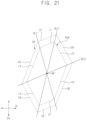
- FIG. 21 is diagram illustrating a unit area and a pixel area included in the display device of FIG. 20 .
- a display device may include a display area DA.
- the display area DA may be an area for displaying an image.
- a portion of the display area DA is illustrated for convenience of illustration.
- the display area DA may be divided into a plurality of unit areas UA'.
- the plurality of unit areas UA' may be defined as a set of minimum units capable of filling the display area DA without blanking or overlapping with each other.
- Each of the plurality of unit areas UA' may have the same or substantially the same shape as each other.
- the unit area UA' may have a hexagonal shape in which each of all interior angles is less than 180 degrees.
- Each of the plurality of unit areas UA' may have a first border defining a boundary of each of the plurality of unit areas UA'.
- the first border may be an imaginary line that is not recognized by a user of the display device.
- the first border may be point-symmetric with respect to a reference point RP' located within the unit area UA'.
- the phrase "the reference point RP' is located within the unit area UA'” may have the same or substantially the same meaning as the phrase "the reference point RP' is surrounded (e.g., around a periphery thereof) by the first border".
- first to third reference lines RL1', RL2', and RL3' that are different from each other may pass through the reference point RP' thorough all vertices of the first border, and each of the first to third reference lines RL1', RL2', and RL3' may bisect an area of the unit area UA'.
- the first border may have a hexagonal shape including a first outer side O1', a second outer side O2', a third outer side O3', a fourth outer side O4', a fifth outer side O5', and a sixth outer side O6'.
- a length of the first outer side O1' may be the same or substantially the same as a length of the second outer side O2', and the first outer side O1' may be parallel to or substantially parallel to the second outer side O2'.
- the first outer side O1' may extend or substantially extend in (e.g., may be parallel to or substantially parallel to) the row direction Dr. Accordingly, the second outer side O2' of one unit area UA' from among two unit areas UA' that are adjacent to each other in the column direction Dc from among the plurality of unit areas UA' may contact the first outer side O1' of the other unit area UA' from among the two unit areas UA'.
- the third outer side O3' and the fourth outer side O4' may connect one end of the first outer side O1' and one end of the second outer side O2' to each other.
- the fifth outer side O5' and the sixth outer side O6' may connect the other end of the first outer side O1' opposite to the one end of the first outer side O1' and other end of the second outer side O2' opposite to the one end of the second outer side O2' to each other.
- a pixel area PXA' may be disposed in each of the plurality of unit areas UA'.
- the pixel area PXA' may have a hexagonal shape in which a size of each of all interior angles is less than 180 degrees.
- the pixel area PXA' may have a second border defining a boundary of the pixel area PXA'.
- the second border may be an imaginary line that is not recognized by a user of the display device. Because the pixel area PXA' is disposed in each of the plurality of unit areas UA', the second border may be disposed inside (e.g., within) the first border. In this case, the second border may be spaced apart from the first border.
- the second border may be point-symmetric with respect to the reference point RP' located within the unit area UA' (e.g., or located within the pixel area PXA').
- the first to third reference lines RL1', RL2', and RL3' that are different from each other and passing through the reference point RP' may pass thorough all vertices of the second border, and each of the first to third reference lines RL1', RL2', and RL3' may bisect an area of the pixel area PXA'.
- the second border may have a hexagonal shape including a first inner side I1' adjacent to the first outer side O1', a second inner side I2' adjacent to the second outer side O2', a third inner side I3' adjacent to the third outer side O3', a fourth inner side I4' adjacent to the fourth outer side O4', a fifth inner side I5' adjacent to the fifth outer side O5', and a sixth inner side I6' adjacent to the sixth outer side O6'.
- the third inner side I3' and the fourth inner side I4' may connect one end of the first inner side I1' and one end of the second inner side I2' to each other.
- the fifth inner side I5' and the sixth inner side I6' may connect the other end of the first inner side I1' opposite to the one end of the first inner side I1' and the other end of the second inner side I2' opposite to the one end of the second inner side I2' to each other.
- first inner side I1' may be parallel to or substantially parallel to the first outer side O1'
- second inner side I2' may be parallel to or substantially parallel to the second outer side O2'
- third inner side I3' may be parallel to or substantially parallel to the third outer side O3'
- fourth inner side I4' may be parallel to or substantially parallel to the fourth outer side O4'
- fifth inner side I5' may be parallel to or substantially parallel to the fifth outer side O5'
- sixth inner side I6' may be parallel to or substantially parallel to the sixth outer side O6'.
- a first sub-pixel area SA1a', a second sub-pixel area SA2a', a third sub-pixel area SA3a', and a fourth sub-pixel area SA4a' may be disposed in the pixel area PXA'.
- Each of the first to fourth sub-pixel areas SA1a', SA2a', SA3a', and SA4a' may be a minimum unit for emitting or substantially emitting light.
- a border of the first sub-pixel area SA1a' may include the first inner side I1'.
- a border of the fourth sub-pixel area SA4a' may include the second inner side I2'. Accordingly, in one or more embodiments of the present disclosure, the fourth sub-pixel area SA4a' disposed in one unit area UA' from among two unit areas UA' that are adjacent to each other in the column direction Dc from among the plurality of unit areas UA' may be adjacent to the first sub-pixel area SA1a' of the other unit area UA' from among the two unit areas UA'.
- a border of the second sub-pixel area SA2a' may include a portion of the second border.
- the second sub-pixel area SA2a' may include a portion of the third inner side I3' adjacent to the fourth inner side I4', and a portion of the fourth inner side I4' adjacent to the third inner side I3'.
- a border of the third sub-pixel area SA3a' may include another portion of the second border.
- the third sub-pixel area SA3a' may include a portion of the fifth inner side I5' adjacent to the sixth inner side I6', and a portion of the sixth inner side I6' adjacent to the fifth inner side I5'.
- the first to fourth sub-pixel areas SA1a', SA2a', SA3a', and SA4a' having a pentagonal shape are illustrated, but the shape of the first to fourth sub-pixel areas SA1a', SA2a', SA3a', and SA4a' is not limited thereto.
- the border of the first sub-pixel area SA1a' and the border of the fourth sub-pixel area SA4a' may have a N-sided polygon shape (where N is 3, 4, 5, or 6).
- N is 3, 4, 5, or 6
- the border of the second sub-pixel area SA2a' and the border of the third sub-pixel area SA3a' may have a M-sided polygon shape (where M is 4 or 5).
- M is 4 or 5
- the border of the first sub-pixel area SA1a' and the border of the fourth sub-pixel area SA4a' may be point-symmetric with each other with respect to the reference point RP'.
- Unit areas UA' arranged along the column direction Dc from among the plurality of unit areas UA' may define a plurality of pixel columns.
- the plurality of pixel columns may include a first pixel column C1', a second pixel column C2' adjacent to the first pixel column C1' in the row direction Dr, and a third pixel column C3' adjacent to the second pixel column C2' in the row direction Dr.
- the second pixel column C2' may be a pixel column in which the first pixel column C1' is shifted by a suitable distance (e.g., a predetermined distance) in the column direction Dc
- the third pixel column C3' may be a pixel column in which the second pixel column C2' is shifted by a suitable distance (e.g., a predetermined distance) in the column direction Dc.
- the plurality of pixel columns may be interlocked with one another, and arranged along the row direction Dr.
- the first pixel column C1' and the second pixel column C2' may be interlocked with each other
- the second pixel column C2' and the third pixel column C3' may be interlocked with each other
- the third pixel column C3' and the first pixel column C1' may be interlocked with each other.
- the first to third pixel columns C1', C2', and C3' may be interlocked with one another, and alternately arranged along the row direction Dr.
- the present invention can be applied to various display devices and manufacturing methods of the display devices.
- the present invention can be applied to various display devices such as display devices for vehicles, ships, and aircraft, portable communication devices, display devices for exhibition or information delivery, medical display devices, etc.
Landscapes
- Engineering & Computer Science (AREA)
- Manufacturing & Machinery (AREA)
- Microelectronics & Electronic Packaging (AREA)
- Chemical & Material Sciences (AREA)
- Chemical Kinetics & Catalysis (AREA)
- Materials Engineering (AREA)
- Mechanical Engineering (AREA)
- Metallurgy (AREA)
- Organic Chemistry (AREA)
- Physics & Mathematics (AREA)
- Geometry (AREA)
- Electroluminescent Light Sources (AREA)
- Devices For Indicating Variable Information By Combining Individual Elements (AREA)
- Physical Vapour Deposition (AREA)
Abstract
Description
- Aspects of one or more embodiments of the present disclosure relate generally to an organic light emitting display device, and a method of manufacturing the same.
- An organic light emitting display device is a device for displaying an image, and may include a pixel, which is a minimum unit for displaying an image. The pixel may include a pixel electrode, a pixel defining layer defining an opening exposing the pixel electrode, an organic light emitting material disposed on the pixel electrode to correspond to the opening, a cathode electrode disposed on the organic light emitting material, and/or the like. The opening of the pixel defining layer may define an area and shape of the pixel by exposing the pixel electrode.
- The organic light emitting material constituting the pixel of the organic light emitting display device may be deposited using a mask including a fine metal mask (FMM). In this case, when a size of one pixel is designed to be relatively small in order to display a high-resolution image in a limited display area, a size of an opening pattern formed in the mask may be very small. Accordingly, it may be difficult to form the opening pattern in the mask, and thus, manufacturing yield of the mask may be reduced.
- Further, in a high-resolution organic light emitting display device, a distance between two adjacent pixels may be relatively short. In this case, when the organic light emitting material is deposited in one opening of the pixel defining layer through the opening pattern of the mask, an end of the deposited organic light emitting material may invade another opening of the pixel defining layer, so that two or more organic light emitting materials may be stacked in the other opening of the pixel defining layer. Accordingly, light emitted by the pixel corresponding to the other opening may emit a plurality of different colored light, so that the colors of the light may be mixed with each other.
- An object of the present invention is to provide a display device capable of displaying a high-resolution image in a limited display area.
- An object of the present invention is to provide a method of manufacturing the display device.
- However, the problem to be solved by the present invention is not limited to the above-mentioned problem, and may be expanded in various ways without departing from the spirit and scope of the present invention.
- According to one or more embodiments of the present disclosure, a display device includes: a plurality of unit areas, each of the plurality of unit areas including a first border having a hexagonal shape including: a first outer side; and a second outer side parallel to the first outer side, and having a length equal to a length of the first outer side; a pixel area in each of the plurality of unit areas, and including a second border having a hexagonal shape including: a first inner side adjacent to the first outer side; and a second inner side adjacent to the second outer side; a first sub-pixel area in the pixel area, a border of the first sub-pixel area including the first inner side; a first light emitting material in the first sub-pixel area; a second sub-pixel area in the pixel area, a border of the second sub-pixel area including a first portion of the second border; a second light emitting material in the second sub-pixel area; a third sub-pixel area in the pixel area, a border of the third sub-pixel area including a second portion of the second border different from the first portion of the second border; a third light emitting material in the third sub-pixel area; a fourth sub-pixel area in the pixel area, a border of the fourth sub-pixel area including the second inner side; and the first light emitting material in the fourth sub-pixel area. The second outer side of one unit area from among two unit areas adjacent to each other in a column direction from among the plurality of unit areas contacts the first outer side of another unit area from among the two unit areas.
- In an embodiment, a plurality of pixel columns defined by unit areas from among the plurality of unit areas arranged in the column direction may be interlocked with each other, and may be arranged along a row direction crossing the column direction.
- In an embodiment, the first border may be point-symmetric with respect to a reference point surrounded by the first border.
- In an embodiment, the first outer side may be parallel to a row direction crossing the column direction; and the first border may be line-symmetric with respect to each of a first reference line passing through the reference point and extending in the row direction, and a second reference line passing through the reference point and extending in the column direction.
- In an embodiment, each of all interior angles of the first border and all interior angles of the second border may be less than 180 degrees.
- In an embodiment, the first border may include: a third outer side contacting one end of the first outer side; a fourth outer side connecting the third outer side to one end of the second outer side; a fifth outer side contacting another end of the first outer side opposite to the one end of the first outer side; and a sixth outer side connecting the fifth outer side to another end of the second outer side opposite to the one end of the second outer side.
- In an embodiment, the second border may include: a third inner side contacting one end of the first inner side; a fourth inner side connecting the third inner side to one end of the second inner side; a fifth inner side contacting another end of the first inner side opposite to the one end of the first inner side; and a sixth inner side connecting the fifth inner side to another end of the second inner side opposite to the one end of the second inner side.
- In an embodiment, the first inner side and the first outer side may be parallel to each other; the second inner side and the second outer side may be parallel to each other; the third inner side and the third outer side may be parallel to each other; the fourth inner side and the fourth outer side may be parallel to each other; the fifth inner side and the fifth outer side may be parallel to each other; and the sixth inner side and the sixth outer side may be parallel to each other.
- In an embodiment, the first inner side and the first outer side may be spaced from each other by a first distance; the second inner side and the second outer side may be spaced from each other by a second distance; the third inner side and the third outer side may be spaced from each other by a third distance; the fourth inner side and the fourth outer side may be spaced from each other by a fourth distance; the fifth inner side and the fifth outer side may be spaced from each other by a fifth distance; the sixth inner side and the sixth outer side may be spaced from each other by a sixth distance; and the first distance, the second distance, the third distance, the fourth distance, the fifth distance, and the sixth distance may be equal to each other.
- In an embodiment, the border of the second sub-pixel area may include a portion of the third inner side adjacent to the fourth inner side, and a portion of the fourth inner side adjacent to the third inner side; and the border of the third sub-pixel area may include a portion of the fifth inner side adjacent to the sixth inner side, and a portion of the sixth inner side adjacent to the fifth inner side.
- In an embodiment, each of the border of the first sub-pixel area and the border of the fourth sub-pixel area may have an N-sided polygon shape, where N is equal to 3, 4, 5, or 6.
- In an embodiment, each of the border of the second sub-pixel area and the border of the third sub-pixel area may have an M-sided polygon shape, where M is equal to 4 or 5.
- In an embodiment, an area of the first sub-pixel area may be the same size as that of an area of the fourth sub-pixel area.
- In an embodiment, an area of the first sub-pixel area may be smaller than an area of the second sub-pixel area, and smaller than an area of the third sub-pixel area; and an area of the fourth sub-pixel area may be smaller than the area of the second sub-pixel area, and smaller than the area of the third sub-pixel area.
- In an embodiment, an area of the third sub-pixel area may be larger than an area of the second sub-pixel area.
- In an embodiment, the first light emitting material may be configured to emit light having a first color; the second light emitting material may be configured to emit light having a second color different from the first color; and the third light emitting material may be configured to emit light having a third color different from each of the first color and the second color.
- In an embodiment, the light of the first color may have a peak wavelength in a range of 510 nanometers or more, and 550 nanometers or less; the light of the second color may have a peak wavelength in a range of 610 nanometers or more, and 650 nanometers or less; and the light of the third color may have a peak wavelength in a range of 440 nanometers or more, and 480 nanometers or less.
- According to one or more embodiments of the present disclosure, a method of manufacturing a display device, includes: forming a pixel defining layer including: a plurality of unit areas, each of the plurality of unit areas including a first border having a hexagonal shape including: a first outer side; and a second outer side parallel to the first outer side, and having a length equal to a length of the first outer side; and a pixel area disposed in each of the plurality of unit areas, and including a second border having a hexagonal shape including: a first inner side adjacent to the first outer side; and a second inner side adjacent to the second outer side; forming a plurality of pixel openings in the pixel defining layer, the plurality of pixel openings including: a first pixel opening defining a first sub-pixel area in the pixel area, a border of the first sub-pixel area including the first inner side; a second pixel opening defining a second sub-pixel area in the pixel area, a border of the second sub-pixel area including a first portion of the second border; a third pixel opening defining a third sub-pixel area in the pixel area, a border of the third sub-pixel area including a second portion of the second border different from the first portion of the second border; and a fourth pixel opening defining a fourth sub-pixel area in the pixel area, a border of the fourth sub-pixel area including the second inner side; depositing a first light emitting material in the first pixel opening and the fourth pixel opening; depositing a second light emitting material in the second pixel opening; and depositing a third light emitting material in the third pixel opening. The second outer side of one unit area from among two unit areas adjacent to each other in a column direction from among the plurality of unit areas contacts the first outer side of another unit area from among the two unit areas.
- In an embodiment, the depositing of the first light emitting material may include disposing a first mask defining a first opening pattern on the pixel defining layer; the depositing of the second light emitting material may include disposing a second mask defining a second opening pattern on the pixel defining layer; and the depositing of the third light emitting material may include disposing a third mask defining a third opening pattern on the pixel defining layer.
- In an embodiment, the first opening pattern may concurrently expose the fourth sub-pixel area of the one unit area from among the two unit areas and the first sub-pixel area of the other unit area from among the two unit areas.
- In an embodiment, an area of the first opening pattern may be 80% or more, and 120% or less of an area of the third opening pattern; and an area of the second opening pattern may be 80% or more, and 120% or less of the area of the third opening pattern.
- The display device according to embodiments of the present disclosure may include a plurality of unit areas, a pixel area disposed in each of the plurality of unit areas, and first to fourth sub-pixel areas disposed in the pixel areas. Accordingly, a high-resolution image may be displayed in a display area having a limited area.
- The method of manufacturing the display device according to embodiments of the present disclosure may include depositing a first light emitting material in first and fourth pixel openings corresponding to first and fourth sub-pixel areas, depositing a second light emitting material in a second pixel opening corresponding to a second sub-pixel area, and depositing a third light emitting material in a third pixel opening corresponding to a third sub-pixel area. In this case, the first light emitting material may be concurrently (e.g., simultaneously) deposited in the fourth pixel opening of one unit area of two adjacent unit areas, and the first pixel opening of another unit area of the two adjacent unit areas. Accordingly, yield of the deposition process may be improved.
- However, the effects of the present invention are not limited to the above-mentioned effects, and may be expanded in various ways without departing from the spirit and scope of the present invention.
-
-
FIG. 1 is a plan view illustrating a display device according to an embodiment. -
FIG. 2 is a diagram illustrating a unit area and a pixel area included in the display device ofFIG. 1 . -
FIG. 3 is a plan view illustrating a sub-pixel area according to a first embodiment. -
FIG. 4 is a cross-sectional view taken along the line I-I' ofFIG. 3 . -
FIG. 5 is a plan view illustrating a sub-pixel area according to a second embodiment. -
FIG. 6 is a plan view illustrating a sub-pixel area according to a third embodiment. -
FIG. 7 is a plan view illustrating a sub-pixel area according to a fourth embodiment. -
FIG. 8 is a plan view illustrating a sub-pixel area according to a fifth embodiment. -
FIG. 9 is a plan view illustrating a sub-pixel area according to a sixth embodiment. -
FIG. 10 is a plan view illustrating a sub-pixel area according to a seventh embodiment. -
FIG. 11 is a plan view illustrating a sub-pixel area according to an eighth embodiment. -
FIGS. 12-19 are diagrams illustrating a method of manufacturing the display device ofFIG. 1 . -
FIG. 20 is a plan view illustrating a display device according to another embodiment. -
FIG. 21 is diagram illustrating a unit area and a pixel area included in the display device ofFIG. 20 . - Hereinafter, embodiments will be described in more detail with reference to the accompanying drawings. Like or similar reference numerals refer to like or similar elements throughout, and duplicated description will be omitted.
-
FIG. 1 is a plan view illustrating a display device according to an embodiment.FIG. 2 is a diagram illustrating a unit area and a pixel area included in the display device ofFIG. 1 . - Referring to
FIG. 1 andFIG. 2 , a display device may include a display area DA. The display area DA may be an area for displaying an image. InFIG. 1 , a portion of the display area DA is illustrated for convenience of illustration. - The display area DA may be divided into a plurality of unit areas UA. The plurality of unit areas UA may be defined as a set of minimum units capable of filling the display area DA without blanking or overlapping with each other. Each of the plurality of unit areas UA may have the same or substantially the same shape as each other. In more detail, in any one unit area UA from among the plurality of unit areas UA, the unit area UA may have a hexagonal shape in which each of all interior angles is less than 180 degrees.
- Each of the plurality of unit areas UA may have a first border defining a boundary of each of the plurality of unit areas UA. The first border may be an imaginary line that is not recognized by a user of the display device.
- In an embodiment, the first border may be point-symmetric with respect to a reference point RP located within (e.g., at a center of) the unit area UA. In this case, the phrase "the reference point RP is located within the unit area UA" may have the same or substantially the same meaning as the phrase "the reference point RP is surrounded (e.g., around a periphery thereof) by the first border". In addition, the first border may be line-symmetric with respect to each of a first reference line RL1 passing (e.g., extending) through the reference point in a row direction Dr, and a second reference line RL2 passing (e.g., extending) through the reference point in a column direction Dc crossing (e.g., perpendicular to or substantially perpendicular to) the row direction Dr.
- In an embodiment, the first border may have a hexagonal shape including a first outer side O1, a second outer side O2, a third outer side O3, a fourth outer side O4, a fifth outer side O5, and a sixth outer side O6.
- A length of the first outer side O1 may be the same or substantially the same as a length of the second outer side O2, and the first outer side O1 may be parallel to or substantially parallel to the second outer side O2. In addition, the first outer side O1 may be parallel to or substantially parallel to the row direction Dr. Accordingly, the second outer side O2 of one unit area UA from among two unit areas UA that are adjacent to each other in the column direction Dc from among the plurality of unit areas UA may contact the first outer side O1 of the other unit area UA from among the two unit areas UA.
- The third outer side O3 and the fourth outer side O4 may connect one end of the first outer side O1 and one end of the second outer side O2 to each other. The fifth outer side O5 and the sixth outer side O6 may connect the other end of the first outer side O1 opposite to the one end of the first outer side O1 and the other end of the second outer side O2 opposite to the one end of the second outer side O2 to each other.
- A pixel area PXA may be disposed in each of the plurality of unit areas UA. The pixel area PXA may have a hexagonal shape in which a size of each of all interior angles is less than 180 degrees.
- The pixel area PXA may have a second border defining a boundary of the pixel area PXA. The second border may be an imaginary line that is not recognized by a user of the display device. Because the pixel area PXA is disposed in each of the plurality of unit areas UA, the second border may be disposed inside (e.g., within) the first border. In this case, the second border may be spaced apart from the first border.
- In an embodiment, the second border may be point-symmetric with respect to the reference point RP located within (e.g., at a center of) the unit area UA (e.g., or within (e.g., at a center of) the pixel area PXA). In addition, the second border may be line-symmetric with respect to each of the first reference line RL1 passing (e.g., extending) through the reference point in the row direction Dr and the second reference line RL2 passing (e.g., extending) through the reference point in the column direction Dc.
- In an embodiment, the second border may have a hexagonal shape including a first inner side I1 adjacent to the first outer side O1, a second inner side I2 adjacent to the second outer side O2, a third inner side I3 adjacent to the third outer side O3, a fourth inner side I4 adjacent to the fourth outer side O4, a fifth inner side I5 adjacent to the fifth outer side O5, and a sixth inner side I6 adjacent to the sixth outer side O6.
- The third inner side I3 and the fourth inner side I4 may connect one end of the first inner side I1 and one end of the second inner side I2 to each other. The fifth inner side I5 and the sixth inner side I6 may connect the other end of the first inner side I1 opposite to the one end of the first inner side I1 and the other end of the second inner side I2 opposite to the one end of the second inner side I2 to each other.
- In an embodiment, the first inner side I1 may be parallel to or substantially parallel to the first outer side O1, the second inner side I2 may be parallel to or substantially parallel to the second outer side O2, the third inner side I3 may be parallel to or substantially parallel to the third outer side O3, the fourth inner side I4 may be parallel to or substantially parallel to the fourth outer side O4, the fifth inner side I5 may be parallel to or substantially parallel to the fifth outer side O5, and the sixth inner side I6 may be parallel to or substantially parallel to the sixth outer side O6.
- In this case, the first inner side I1 may be spaced apart from the first outer side O1 by a first distance D1, the second inner side I2 may be spaced apart from the second outer side O2 by a second distance D2, the third inner side I3 may be spaced apart from the third outer side O3 by a third distance D3, the fourth inner side I4 may be spaced apart from the fourth outer side O4 by a fourth distance D4, the fifth inner side I5 may be spaced apart from the fifth outer side O5 by a fifth distance D5, and the sixth inner side I6 may be spaced apart from the sixth outer side O6 by a sixth distance D6.
- In an embodiment, the first distance D1, the second distance D2, the third distance D3, the fourth distance D4, the fifth distance D5, and the sixth distance D6 may be identical or substantially identical to each other.
- A first sub-pixel area SA1a, a second sub-pixel area SA2a, a third sub-pixel area SA3a, and a fourth sub-pixel area SA4a may be disposed in the pixel area PXA. Each of the first to fourth sub-pixel areas SA1a, SA2a, SA3a, and SA4a may be a minimum unit for emitting or substantially emitting light. For example, each of the first to fourth sub-pixel areas SA1a, SA2a, SA3a, and SA4a may correspond to an opening of a pixel defining layer (e.g., refer to PDL of
FIG. 4 ), and a light emitting material may be disposed in the opening. This will be described in more detail below with reference toFIG. 3 andFIG. 4 . - A border of the first sub-pixel area SA1a may include the first inner side I1. A border of the fourth sub-pixel area SA4a may include the second inner side I2. Accordingly, in one or more embodiments of the present disclosure, the fourth sub-pixel area SA4a disposed in one unit area UA from among two unit areas UA that are adjacent to each other in the column direction Dc from among the plurality of unit areas UA may be adjacent to the first sub-pixel area SA1a of the other unit area UA from among the two unit areas UA.
- A border of the second sub-pixel area SA2a may include a portion of the second border. For example, the second sub-pixel area SA2a may include a portion of the third inner side I3 adjacent to the fourth inner side I4, and a portion of the fourth inner side I4 adjacent to the third inner side I3.
- A border of the third sub-pixel area SA3a may include another portion of the second border. For example, the third sub-pixel area SA3a may include a portion of the fifth inner side I5 adjacent to the sixth inner side I6, and a portion of the sixth inner side I6 adjacent to the fifth inner side I5.
- Unit areas UA arranged in the column direction Dc from among the plurality of unit areas UA may define a plurality of pixel columns. For example, the plurality of pixel columns may include a first pixel column C1, and a second pixel column C2 adjacent to the first pixel column C1 in the row direction Dr. The second pixel column C2 may be a pixel column in which the first pixel column C1 is shifted by a suitable distance (e.g., a predetermined distance) in the column direction Dc.
- The plurality of pixel columns may be interlocked with one another, and arranged along the row direction Dr. For example, the first pixel column C1 and the second pixel column C2 may be interlocked with each other, and alternately arranged along the row direction Dr.
-
FIG. 3 is a plan view illustrating a sub-pixel area according to a first embodiment.FIG. 4 is a cross-sectional view taken along the line I-I' ofFIG. 3 . - The unit area UA, the pixel area PXA, and the first to fourth sub-pixel areas SA1a, SA2a, SA3a, and SA4a illustrated in
FIG. 3 may be the same or substantially the same as the unit area UA, the pixel area PXA, and the first to fourth sub-pixel areas SA1a, SA2a, SA3a, and SA4a described above with reference toFIG. 1 andFIG. 2 , and thus, redundant description thereof may not be repeated. - Referring to
FIG. 3 andFIG. 4 , the display device may include a substrate SUB, first to fourth pixel electrodes PXE1, PXE2, PXE3, and PXE4, a pixel defining layer PDL, and first to third light emitting materials EL1, EL2, and EL3. - The substrate SUB may include a plurality of insulation layers, and a plurality of transistors. In an embodiment, the substrate SUB may include a material having flexibility, so as to be repeatedly folded and/or unfolded.
- The first to fourth pixel electrodes PXE1, PXE2, PXE3, and PXE4 may be disposed on the substrate SUB. The first to fourth pixel electrodes PXE1, PXE2, PXE3, and PXE4 may be disposed to be spaced apart from each other. The first to fourth pixel electrodes PXE1, PXE2, PXE3, and PXE4 may be disposed in the unit area UA. Each of the first to fourth pixel electrodes PXE1, PXE2, PXE3, and PXE4 may be electrically connected to the plurality of transistors. In an embodiment, each of the first to fourth pixel electrodes PXE1, PXE2, PXE3, and PXE4 may be referred to as an anode electrode.
- The pixel defining layer PDL may be disposed on the first to fourth pixel electrodes PXE1, PXE2, PXE3, and PXE4. The pixel defining layer PDL may include an organic material. The pixel defining layer PDL may define an opening exposing each of the first to fourth pixel electrodes PXE1, PXE2, PXE3, and PXE4. The opening may include a first pixel opening exposing the first pixel electrode PXE1, a second pixel opening exposing the second pixel electrode PXE2, a third pixel opening exposing the third pixel electrode PXE3, and a fourth pixel opening exposing the fourth pixel electrode PXE4.
- The first to third light emitting materials EL1, EL2, and EL3 may include a suitable material for emitting light. For example, the first to third light emitting materials EL1, EL2, and EL3 may include an organic light emitting material. The first to third light emitting materials EL1, EL2, and EL3 may be disposed in the opening. In more detail, the first light emitting material EL1 may be disposed in the first pixel opening and the fourth pixel opening, the second light emitting material EL2 may be disposed in the second pixel opening, and the third light emitting material EL3 may be disposed in the third pixel opening.
- In an embodiment, the first to third light emitting materials EL1, EL2, and EL3 may be further disposed on the pixel defining layer PDL. In this case, an area in which the first light emitting material EL1 may be located may be a first area A1a and a fourth area A4a, an area in which the second light emitting material EL2 may be located may be a second area A2a, and an area in which the third light emitting material EL3 may be located may be a third area A3a. The first to fourth areas A1a, A2a, A3a, and A4a may be disposed in the unit area UA. In an embodiment, an entire outer border of the first to fourth areas A1a, A2a, A3a, and A4a may be the same or substantially the same as the first border of the unit area UA.
- In an embodiment, the first light emitting material EL1 may emit light having a first color, the second light emitting material EL2 may emit light having a second color, and the third light emitting material EL3 may emit light having a third color. In this case, the light of the first color may have a peak wavelength in a range of about 510 nm or more and about 550 nm or less, the light of the second color may have a peak wavelength in a range of about 610 nm or more and about 650 nm or less, and the light of the third color may have a peak wavelength in a range of about 440 nm or more and about 480 nm or less. In other words, the first color may be green, the second color may be red, and the third color may be blue.
- Although not shown in
FIG. 3 andFIG. 4 , a common electrode covering the first to third light emitting materials EL1, EL2, and EL3 may be disposed on the pixel defining layer PDL. The common electrode may include a transparent conductive material. In an embodiment, the common electrode may be referred to as a cathode electrode. - The first sub-pixel area SA1a may be defined as an area corresponding to the first pixel opening. The first sub-pixel area SA1a may be an area in which light is emitted or substantially emitted from the first light emitting material EL1 among the first area A1a.
- The first sub-pixel area SA1a may have a pentagonal shape. In this case, a border of the first sub-pixel area SA1a may include the first inner side I1, a portion of the third inner side I3 adjacent to the first inner side I1, and a portion of the fifth inner side I5 adjacent to the first inner side I1.
- When the first sub-pixel area SA1a has the pentagonal shape, the first area A1a may have a pentagonal shape. In this case, a border of the first area A1a may surround (e.g., around a periphery of) the border of the first sub-pixel area SA1a.
- The second sub-pixel area SA2a may be defined as an area corresponding to the second pixel opening. The second sub-pixel area SA2a may be an area in which light is emitted or substantially emitted from the second light emitting material EL2 among the second area A2a.
- The second sub-pixel area SA2a may have a pentagonal shape. In this case, a border of the second sub-pixel area SA2a may include a portion of the third inner side I3 adjacent to the fourth inner side I4, and a portion of the fourth inner side I4 adjacent to the third inner side I3.
- When the second sub-pixel area SA2a has the pentagonal shape, the second area A2a may have a pentagonal shape. In this case, a border of the second area A2a may surround (e.g., around a periphery of) the border of the second sub-pixel area SA2a.
- The third sub-pixel area SA3a may be defined as an area corresponding to the third pixel opening. The third sub-pixel area SA3a may be an area in which light is emitted or substantially emitted from the third light emitting material EL3 among the third area A3a.
- The third sub-pixel area SA3a may have a pentagonal shape. In this case, a border of the third sub-pixel area SA3a may include a portion of the fifth inner side I5 adjacent to the sixth inner side I6, and a portion of the sixth inner side I6 adjacent to the fifth inner side I5.
- When the third sub-pixel area SA3a has the pentagonal shape, the third area A3a may have a pentagonal shape. In this case, a border of the third area A3a may surround (e.g., around a periphery of) the third sub-pixel area SA3a.
- The fourth sub-pixel area SA4a may be defined as an area corresponding to the fourth pixel opening. The fourth sub-pixel area SA4a may be an area in which light is emitted or substantially emitted from the first light emitting material EL1 among the fourth area A4a.
- The fourth sub-pixel area SA4a may have a pentagonal shape. In this case, a border of the fourth sub-pixel area SA4a may include the second inner side I2, a portion of the fourth inner side I4 adjacent to the second inner side I2, and a portion of the sixth inner side I6 adjacent to the second inner side I2.
- In an embodiment, the border of the fourth sub-pixel area SA4a and the border of the first sub-pixel area SA1a may be line-symmetric with each other with respect to the first reference line RL1 described above with reference to
FIG. 2 . - When the fourth-sub-pixel area SA4a has the pentagonal shape, the fourth area A4a may have a pentagonal shape. In this case, a border of the fourth area SA4a may surround (e.g., around a periphery of) the fourth sub-pixel area SA4a.
- In order to increase or maximize luminous efficiency of the first to third light emitting materials EL1, EL2, and EL3, each of the first to fourth sub-pixel areas SA1a, SA2a, SA3a, and SA4a may have various suitable areas.
- In an embodiment, an area of the first sub-pixel area SA1a may be the same or substantially the same as an area of the fourth sub-pixel area SA4a.
- In an embodiment, an area of the second sub-pixel area SA2a may be different from an area of the third sub-pixel area SA3a. For example, the area of the third sub-pixel area SA3a may be larger than the area of the second sub-pixel area SA2a. As another example, the area of the third sub-pixel area SA3a may be smaller than the area of the second sub-pixel area SA2a.
- In an embodiment, the area of the first sub-pixel area SA1a may be smaller than the area of the second sub-pixel area SA2a, and may be smaller than the area of the third sub-pixel area SA3a. In addition, the area of the fourth sub-pixel area SA4a may be smaller than the area of the second sub-pixel area SA2a, and may be smaller than the area of the third sub-pixel area SA3a.
-
FIG. 5 is a plan view illustrating a sub-pixel area according to a second embodiment. - The unit area UA and the pixel area PXA illustrated in
FIG. 5 may be the same or substantially same as (or similar to) the unit area UA and the pixel area PXA described above with reference toFIG. 1 andFIG. 2 , and thus, redundant description thereof may not be repeated. - Referring to
FIG. 5 , first to fourth sub-pixel areas SA1b, SA2b, SA3b, and SA4b according to the second embodiment may be the same or substantially the same as (or similar to) the first to fourth sub-pixel areas SA1a, SA2a, SA3a, and SA4a described above with reference toFIG. 3 andFIG. 4 , except for a planar shape thereof. In addition, first to fourth areas A1b, A2b, A3b, and A4b according to the second embodiment may be the same or substantially same as the first to fourth areas A1a, A2a, A3a, and A4a described above with reference toFIG. 3 andFIG. 4 , except for a planar shape thereof. Accordingly, redundant description thereof may not be repeated, and the differences therebetween may be mainly described hereinafter. - The first sub-pixel area SA1b may have a pentagonal shape. In this case, a border of the first sub-pixel area SA1b may include the first inner side I1, a portion of the third inner side I3 adjacent to the first inner side I1, and a portion of the fifth inner side I5 adjacent to the first inner side I1.
- When the first sub-pixel area SA1b has the pentagonal shape, the first area A1b may have a pentagonal shape. In this case, a border of the first area A1b may surround (e.g., around a periphery of) the border of the first sub-pixel area SA1b.
- The second sub-pixel area SA2b may have a quadrangular shape. In this case, a border of the second sub-pixel area SA2b may include a portion of the third inner side I3 adjacent to the fourth inner side I4, and a portion of the fourth inner side I4 adjacent to the third inner side I3.
- When the second sub-pixel area SA2b has the quadrangular shape, the second area A2b may have a quadrangular shape. In this case, a border of the second area A2b may surround (e.g., around a periphery of) the border of the second sub-pixel area SA2b.
- The third sub-pixel area SA3b may have a quadrangular shape. In this case, a border of the third sub-pixel area SA3b may include a portion of the fifth inner side I5 adjacent to the sixth inner side I6, and a portion of the sixth inner side I6 adjacent to the fifth inner side I5.
- When the third sub-pixel area SA3b has the quadrangular shape, the third area A3b may have a quadrangular shape. In this case, a border of the third area A3b may surround (e.g., around a periphery of) the border of the third sub-pixel area SA3a.
- The fourth sub-pixel area SA4b may have a pentagonal shape. In this case, a border of the fourth sub-pixel area SA4b may include the second inner side I2, a portion of the fourth inner side I4 adjacent to the second inner side I2, and a portion of the sixth inner side I6 adjacent to the second inner side I2.
- In an embodiment, the border of the fourth sub-pixel area SA4b and the border of the first sub-pixel area SA1b may be line-symmetric with each other with respect to the first reference line RL1 described above with reference to
FIG. 2 . - When the fourth sub-pixel area SA4b has the pentagonal shape, the fourth area SA4b may have a pentagonal shape. In this case, a border of the fourth area A4b may surround (e.g., around a periphery of) the border of the fourth sub-pixel area SA4b.
- Each of the first to fourth sub-pixel areas SA1b, SA2b, SA3b, and SA4b may have various suitable areas.
- In an embodiment, an area of the first sub-pixel area SA1b may be the same or substantially the same as an area of the fourth sub-pixel area SA4b.
- In an embodiment, an area of the second sub-pixel area SA2b may be different from an area of the third sub-pixel area SA3b. For example, the area of the third sub-pixel area SA3b may be larger than the area of the second sub-pixel area SA2b. As another example, the area of the third sub-pixel area SA3b may be smaller than the area of the second sub-pixel area SA2b.
- In an embodiment, the area of the first sub-pixel area SA1b may be smaller than the area of the second sub-pixel area SA2b, and may be smaller than the area of the third sub-pixel area SA3b. In addition, the area of the fourth sub-pixel area SA4b may be smaller than the area of the second sub-pixel area SA2b, and may be smaller than the area of the third sub-pixel area SA3b.
-
FIG. 6 is a plan view illustrating a sub-pixel area according to a third embodiment. - The unit area UA and the pixel area PXA illustrated in
FIG. 6 may be the same or substantially the same as the unit area UA and the pixel area PXA described above with reference toFIG. 1 andFIG. 2 , and thus, redundant description thereof may not be repeated. - Referring to
FIG. 6 , first to fourth sub-pixel areas SA1c, SA2c, SA3c, and SA4c according to the third embodiment may be the same or substantially the same as the first to fourth sub-pixel areas SA1a, SA2a, SA3a, and SA4a described above with reference toFIG. 3 andFIG. 4 , except for a planar shape thereof. In addition, first to fourth areas A1c, A2c, A3c, and A4c according to the third embodiment may be the same or substantially the same as the first to fourth areas A1a, A2a, A3a, and A4a described above with reference toFIG. 3 andFIG. 4 , except for a planar shape thereof. Accordingly, redundant description thereof may not be repeated, and the differences therebetween may be mainly described hereinafter. - The first sub-pixel area SA1c may have a quadrangular shape. In this case, a border of the first sub-pixel area SA1c may include the first inner side I1, a portion of the third inner side I3 adjacent to the first inner side I1, and a portion of the fifth inner side I5 adjacent to the first inner side I1.
- When the first sub-pixel area SA1c has the quadrangular shape, the first area A1c may have a quadrangular shape. In this case, a border of the first area A1c may surround (e.g., around a periphery of) the border of the first sub-pixel area SA1c.
- The second sub-pixel area SA2c may have a pentagonal shape. In this case, a border of the second sub-pixel area SA2c may include a portion of the third inner side I3 adjacent to the fourth inner side I4, and a portion of the fourth inner side I4 adjacent to the third inner side I3.
- When the second sub-pixel area SA2c has the pentagonal shape, the second area A2c may have a pentagonal shape. In this case, a border of the second area A2c may surround (e.g., around a periphery of) the border of the second sub-pixel area SA2c.
- The third sub-pixel area SA3c may have a pentagonal shape. In this case, a border of the third sub-pixel area SA3c may include a portion of the fifth inner side I5 adjacent to the sixth inner side I6 and a portion of the sixth inner side I6 adjacent to the fifth inner side I5.
- When the third sub-pixel area SA3c has the pentagonal shape, the third area A3c may have a pentagonal shape. In this case, a border of the third area A3c may surround (e.g., around a periphery of) the third sub-pixel area SA3c.
- The fourth sub-pixel area SA4c may have a quadrangular shape. In this case, a border of the fourth sub-pixel area SA4c may include the second inner side I2, a portion of the fourth inner side I4 adjacent to the second inner side I2, and a portion of the sixth inner side I6 adjacent to the second inner side I2.
- In an embodiment, the border of the fourth sub-pixel area SA4c and the border of the first sub-pixel area SA1c may be line-symmetric with each other with respect to the first reference line RL1 described above with reference to
FIG. 2 . In addition, each of the border of the fourth sub-pixel area SA4c and the border of the first sub-pixel area SA1c may be line-symmetric with each other with respect to the second reference line RL2 described above with reference toFIG. 2 . - When the fourth sub-pixel area SA4c has the quadrangular shape, the fourth area A4c may have a quadrangular shape. In this case, a border of the fourth area A4c may surround (e.g., around a periphery of) the border of the fourth sub-pixel area SA4c.
- Each of the first to fourth sub-pixel areas SA1c, SA2c, SA3c, and SA4c may have various suitable areas.
- In an embodiment, an area of the first sub-pixel area SA1c may be the same or substantially the same as an area of the fourth sub-pixel area SA4c.
- In an embodiment, an area of the second sub-pixel area SA2c may be different from an area of the third sub-pixel area SA3c. For example, the area of the third sub-pixel area SA3c may be larger than the area of the second sub-pixel area SA2c. As another example, the area of the third sub-pixel area SA3c may be smaller than the area of the second sub-pixel area SA2c.
- In an embodiment, the area of the first sub-pixel area SA1c may be smaller than the area of the second sub-pixel area SA2c, and may be smaller than the area of the third sub-pixel area SA3c. In addition, the area of the fourth sub-pixel area SA4c may be smaller than the area of the second sub-pixel area SA2c, and may be smaller than the area of the third sub-pixel area SA3c.
-
FIG. 7 is a plan view illustrating a sub-pixel area according to a fourth embodiment. - The unit area UA and the pixel area PXA illustrated in
FIG. 7 may be the same or substantially the same as the unit area UA and the pixel area PXA described above with reference toFIG. 1 andFIG. 2 , and thus, redundant description thereof may not be repeated. - Referring to
FIG. 7 , first to fourth sub-pixel areas SA1d, SA2d, SA3d, and SA4d according to the fourth embodiment may be the same or substantially same as the first to fourth sub-pixel areas SA1a, SA2a, SA3a, and SA4a described above with reference toFIG. 3 andFIG. 4 , except for a planar shape thereof. In addition, first to fourth areas A1d, A2d, A3d, and A4d according to the fourth embodiment may be the same or substantially the same as the first to fourth areas A1a, A2a, A3a, and A4a described above with reference toFIG. 3 andFIG. 4 , except for a planar shape thereof. Accordingly, redundant description thereof may not be repeated, and the differences therebetween may be mainly described hereinafter. - The first sub-pixel area SA1d may have a quadrangular shape. In this case, a border of the first sub-pixel area SA1d may include the first inner side I1, a portion of the third inner side I3 adjacent to the first inner side I1, and a portion of the fifth inner side I5 adjacent to the first inner side I1.
- When the first sub-pixel area SA1d has the quadrangular shape, the first area A1d may have a quadrangular shape. In this case, a border of the first area A1d may surround (e.g., around a periphery of) the border of the first sub-pixel area SA1d.
- The second sub-pixel area SA2d may have a quadrangular shape. In this case, a border of the second sub-pixel area SA2d may include a portion of the third inner side I3 adjacent to the fourth inner side I4, and a portion of the fourth inner side I4 adjacent to the third inner side I3.
- When the second sub-pixel area SA2d has the quadrangular shape, the second area A2d may have a pentagonal shape. In this case, a border of the second area A2c may surround (e.g., around a periphery of) the border of the second sub-pixel area SA2c.
- The third sub-pixel area SA3d may have a quadrangular shape. In this case, a border of the third sub-pixel area SA3d may include a portion of the fifth inner side I5 adjacent to the sixth inner side I6, and a portion of the sixth inner side I6 adjacent to the fifth inner side I5.
- When the third sub-pixel area SA3d has the quadrangular shape, the third area A3d may have a pentagonal shape. In this case, a border of the third area A3d may surround (e.g., around a periphery of) the third sub-pixel area SA3d.
- The fourth sub-pixel area SA4d may have a quadrangular shape. In this case, a border of the fourth sub-pixel area SA4d may include the second inner side I2, a portion of the fourth inner side I4 adjacent to the second inner side I2, and a portion of the sixth inner side I6 adjacent to the second inner side I2.
- In an embodiment, the border of the fourth sub-pixel area SA4d and the border of the first sub-pixel area SA1d may be line-symmetric with each other with respect to the first reference line RL1 described above with reference to
FIG. 2 . In addition, each of the border of the fourth sub-pixel area SA4d and the border of the first sub-pixel area SA1d may be line-symmetric with each other with respect to the second reference line RL2 described above with reference toFIG. 2 . - When the fourth sub-pixel area SA4d has the quadrangular shape, the fourth area A4d may have a quadrangular shape. In this case, a border of the fourth area A4d may surround (e.g., around a periphery of) the border of the fourth sub-pixel area SA4d.
- Each of the first to fourth sub-pixel areas SA1d, SA2d, SA3d, and SA4d may have various suitable areas.
- In an embodiment, an area of the first sub-pixel area SA1d may be the same or substantially the same as an area of the fourth sub-pixel area SA4d.
- In an embodiment, an area of the second sub-pixel area SA2d may be different from an area of the third sub-pixel area SA3d. For example, the area of the third sub-pixel area SA3d may be larger than the area of the second sub-pixel area SA2d. As another example, the area of the third sub-pixel area SA3d may be smaller than the area of the second sub-pixel area SA2d.
- In an embodiment, the area of the first sub-pixel area SA1d may be smaller than the area of the second sub-pixel area SA2d, and may be smaller than the area of the third sub-pixel area SA3d. In addition, the area of the fourth sub-pixel area SA4d may be smaller than the area of the second sub-pixel area SA2d, and may be smaller than the area of the third sub-pixel area SA3d.
-
FIG. 8 is a plan view illustrating a sub-pixel area according to a fifth embodiment. - The unit area UA and the pixel area PXA illustrated in
FIG. 8 may be the same or substantially the same as the unit area UA and the pixel area PXA described above with reference toFIG. 1 andFIG. 2 , and thus, redundant description thereof may not be repeated. - Referring to
FIG. 8 , first to fourth sub-pixel areas SA1e, SA2e, SA3e, and SA4e according to the fifth embodiment may be the same or substantially the same as the first to fourth sub-pixel areas SA1a, SA2a, SA3a, and SA4a described above with reference toFIG. 3 andFIG. 4 , except for a planar shape thereof. In addition, first to fourth areas A1e, A2e, A3e, and A4e according to the fifth embodiment may be the same or substantially same as the first to fourth areas A1a, A2a, A3a, and A4a described above with reference toFIG. 3 andFIG. 4 , except for a planar shape thereof. Accordingly, redundant description thereof may not be repeated, and the differences therebetween may be mainly described hereinafter. - The first sub-pixel area SA1e may have a quadrangular shape. In this case, a border of the first sub-pixel area SA1e may include the first inner side I1, and a portion of the fifth inner side I5 adjacent to the first inner side I1.
- When the first sub-pixel area SA1e has the quadrangular shape, the first area A1e may have a pentagonal shape. In this case, a border of the first area A1e may surround (e.g., around a periphery of) the border of the first sub-pixel area SA1e.
- The second sub-pixel area SA2e may have a pentagonal shape. In this case, a border of the second sub-pixel area SA2e may include a portion of the third inner side I3 adjacent to the fourth inner side I4, and a portion of the fourth inner side I4 adjacent to the third inner side I3.
- When the second sub-pixel area SA2e has the pentagonal shape, the second area A2e may have a pentagonal shape. In this case, a border of the second area A2e may surround (e.g., around a periphery of) the border of the second sub-pixel area SA2e.
- The third sub-pixel area SA3e may have a pentagonal shape. In this case, a border of the third sub-pixel area SA3e may include a portion of the fifth inner side I5 adjacent to the sixth inner side I6, and a portion of the sixth inner side I6 adjacent to the fifth inner side I5.
- When the third sub-pixel area SA3e has the pentagonal shape, the third area A3e may have a pentagonal shape. In this case, a border of the third area A3e may surround (e.g., around a periphery of) the third sub-pixel area SA3e.
- The fourth sub-pixel area SA4e may have a quadrangular shape. In this case, a border of the fourth sub-pixel area SA4e may include the second inner side I2, and a portion of the sixth inner side I6 adjacent to the second inner side I2.
- In an embodiment, the border of the fourth sub-pixel area SA4e and the border of the first sub-pixel area SA1e may be line-symmetric with each other with respect to the first reference line RL1 described above with reference to
FIG. 2 . - When the fourth sub-pixel area SA4d has the quadrangular shape, the fourth area A4d may have a pentagonal shape. In this case, a border of the fourth area A4e may surround (e.g., around a periphery of) the border of the fourth sub-pixel area SA4e.
- Each of the first to fourth sub-pixel areas SA1e, SA2e, SA3e, and SA4e may have various suitable areas.
- In an embodiment, an area of the first sub-pixel area SA1e may be the same or substantially the same as an area of the fourth sub-pixel area SA4e.
- In an embodiment, an area of the second sub-pixel area SA2e may be different from an area of the third sub-pixel area SA3e. For example, the area of the third sub-pixel area SA3e may be larger than the area of the second sub-pixel area SA2e. As another example, the area of the third sub-pixel area SA3e may be smaller than the area of the second sub-pixel area SA2e.
- In an embodiment, the area of the first sub-pixel area SA1e may be smaller than the area of the second sub-pixel area SA2e, and may be smaller than the area of the third sub-pixel area SA3e. In addition, the area of the fourth sub-pixel area SA4e may be smaller than the area of the second sub-pixel area SA2e, and may be smaller than the area of the third sub-pixel area SA3e.
-
FIG. 9 is a plan view illustrating a sub-pixel area according to a sixth embodiment. - The unit area UA and the pixel area PXA illustrated in
FIG. 9 may be the same or substantially the same as the unit area UA and the pixel area PXA described above with reference toFIG. 1 andFIG. 2 , and thus, redundant description thereof may not be repeated. - Referring to
FIG. 9 , first to fourth sub-pixel areas SA1f, SA2f, SA3f, and SA4f according to the sixth embodiment may be the same or substantially the same as the first to fourth sub-pixel areas SA1a, SA2a, SA3a, and SA4a described above with reference toFIG. 3 andFIG. 4 , except for a planar shape thereof. In addition, first to fourth areas A1f, A2f, A3f, and A4f according to the sixth embodiment may be the same or substantially the same as the first to fourth areas A1a, A2a, A3a, and A4a described above with reference toFIG. 3 andFIG. 4 , except for a planar shape thereof. Accordingly, redundant description thereof may not be repeated, and the differences therebetween may be mainly described hereinafter. - The first sub-pixel area SA1f may have a hexagonal shape. In this case, a border of the first sub-pixel area SA1f may include the first inner side I1, a portion of the third inner side I3 adjacent to the first inner side I1, and a portion of the fifth inner side I5 adjacent to the first inner side I1.
- When the first sub-pixel area SA1f has the hexagonal shape, the first area A1f may have a pentagonal shape. In this case, a border of the first area A1f may surround (e.g., around a periphery of) the border of the first sub-pixel area SA1f.
- The second sub-pixel area SA2f may have a pentagonal shape. In this case, a border of the second sub-pixel area SA2f may include a portion of the third inner side I3 adjacent to the fourth inner side I4, and a portion of the fourth inner side I4 adjacent to the third inner side I3.
- When the second sub-pixel area SA2f has the pentagonal shape, the second area A2f may have a pentagonal shape. In this case, a border of the second area A2f may surround (e.g., around a periphery of) the border of the second sub-pixel area SA2f.
- The third sub-pixel area SA3f may have a pentagonal shape. In this case, a border of the third sub-pixel area SA3f may include a portion of the fifth inner side I5 adjacent to the sixth inner side I6, and a portion of the sixth inner side I6 adjacent to the fifth inner side I5.
- When the third sub-pixel area SA3f has the pentagonal shape, the third area A3f may have a pentagonal shape. In this case, a border of the third area A3f may surround (e.g., around a periphery of) the third sub-pixel area SA3f.
- The fourth sub-pixel area SA4f may have a hexagonal shape. In this case, a border of the fourth sub-pixel area SA4f may include the second inner side I2, a portion of the fourth inner side I4 adjacent to the second inner side I2, and a portion of the sixth inner side I6 adjacent to the second inner side I2.
- In an embodiment, the border of the fourth sub-pixel area SA4f and the border of the first sub-pixel area SA1f may be line-symmetric with each other with respect to the first reference line RL1 described above with reference to
FIG. 2 . - When the fourth sub-pixel area SA4f has the hexagonal shape, the fourth area A4f may have a pentagonal shape. In this case, a border of the fourth area A4f may surround (e.g., around a periphery of) the border of the fourth sub-pixel area SA4f.
- Each of the first to fourth sub-pixel areas SA1f, SA2f, SA3f, and SA4f may have various suitable areas.
- In an embodiment, an area of the first sub-pixel area SA1f may be the same or substantially the same as an area of the fourth sub-pixel area SA4f.
- In an embodiment, an area of the second sub-pixel area SA2f may be different from an area of the third sub-pixel area SA3f. For example, the area of the third sub-pixel area SA3f may be larger than the area of the second sub-pixel area SA2f. As another example, the area of the third sub-pixel area SA3f may be smaller than the area of the second sub-pixel area SA2f.
- In an embodiment, the area of the first sub-pixel area SA1f may be smaller than the area of the second sub-pixel area SA2f, and may be smaller than the area of the third sub-pixel area SA3f. In addition, the area of the fourth sub-pixel area SA4f may be smaller than the area of the second sub-pixel area SA2f, and may be smaller than the area of the third sub-pixel area SA3f.
-
FIG. 10 is a plan view illustrating a sub-pixel area according to a seventh embodiment. - The unit area UA and the pixel area PXA illustrated in
FIG. 10 may be the same or substantially the same as the unit area UA and the pixel area PXA described above with reference toFIG. 1 andFIG. 2 , and thus, redundant description thereof may not be repeated. - Referring to
FIG. 10 , first to fourth sub-pixel areas SA1g, SA2g, SA3g, and SA4g according to the seventh embodiment may be the same or substantially the same as the first to fourth sub-pixel areas SA1a, SA2a, SA3a, and SA4a described above with reference toFIG. 3 andFIG. 4 , except for a planar shape thereof. In addition, first to fourth areas A1g, A2g, A3g, and A4g according to the seventh embodiment may be the same or substantially the same as the first to fourth areas A1a, A2a, A3a, and A4a described above with reference toFIG. 3 andFIG. 4 , except for a planar shape thereof. Accordingly, redundant description thereof may not be repeated, and the differences therebetween may be mainly described hereinafter. - The first sub-pixel area SA1g may have a triangle shape. In this case, a border of the first sub-pixel area SA1g may include the first inner side I1.
- When the first sub-pixel area SA1g has the triangle shape, the first area A1g may have a pentagonal shape. In this case, a border of the first area A1g may surround (e.g., around a periphery of) the border of the first sub-pixel area SA1g.
- The second sub-pixel area SA2g may have a pentagonal shape. In this case, a border of the second sub-pixel area SA2g may include a portion of the third inner side I3 adjacent to the fourth inner side I4, and a portion of the fourth inner side I4 adjacent to the third inner side I3.
- When the second sub-pixel area SA2g has the pentagonal shape, the second area A2g may have a pentagonal shape. In this case, a border of the second area A2g may surround (e.g., around a periphery of) the border of the second sub-pixel area SA2g.
- The third sub-pixel area SA3g may have a pentagonal shape. In this case, a border of the third sub-pixel area SA3g may include a portion of the fifth inner side I5 adjacent to the sixth inner side I6, and a portion of the sixth inner side I6 adjacent to the fifth inner side I5.
- When the third sub-pixel area SA3g has the pentagonal shape, the third area A3g may have a pentagonal shape. In this case, a border of the third area A3g may surround (e.g., around a periphery of) the third sub-pixel area SA3g.
- The fourth sub-pixel area SA4g may have a triangle shape. In this case, a border of the fourth sub-pixel area SA4g may include the second inner side I2.
- In an embodiment, the border of the fourth sub-pixel area SA4g and the border of the first sub-pixel area SA1g may be line-symmetric with each other with respect to the first reference line RL1 described above with reference to
FIG. 2 . - When the fourth sub-pixel area SA4g has the triangle shape, the fourth area A4g may have a pentagonal shape. In this case, a border of the fourth area A4g may surround (e.g., around a periphery of) the border of the fourth sub-pixel area SA4g.
- Each of the first to fourth sub-pixel areas SA1g, SA2g, SA3g, and SA4g may have various suitable areas.
- In an embodiment, an area of the first sub-pixel area SA1g may be the same or substantially the same as an area of the fourth sub-pixel area SA4g.
- In an embodiment, an area of the second sub-pixel area SA2g may be different from an area of the third sub-pixel area SA3g. For example, the area of the third sub-pixel area SA3g may be larger than the area of the second sub-pixel area SA2g. As another example, the area of the third sub-pixel area SA3g may be smaller than the area of the second sub-pixel area SA2g.
- In an embodiment, the area of the first sub-pixel area SA1g may be smaller than the area of the second sub-pixel area SA2g, and may be smaller than the area of the third sub-pixel area SA3g. In addition, the area of the fourth sub-pixel area SA4g may be smaller than the area of the second sub-pixel area SA2g, and may be smaller than the area of the third sub-pixel area SA3g.
-
FIG. 11 is a plan view illustrating a sub-pixel area according to an eighth embodiment. - The unit area UA and the pixel area PXA illustrated in
FIG. 11 may be the same or substantially the same as the unit area UA and the pixel area PXA described above with reference toFIG. 1 andFIG. 2 , and thus, redundant description thereof may not be repeated. - Referring to
FIG. 11 , first to fourth sub-pixel areas SA1h, SA2h, SA3h, and SA4h according to the eighth embodiment may be the same or substantially the same as the first to fourth sub-pixel areas SA1a, SA2a, SA3a, and SA4a described above with reference toFIG. 3 andFIG. 4 , except for a planar shape thereof. In addition, first to fourth areas A1h, A2h, A3h, and A4h according to the eighth embodiment may be the same or substantially the same as the first to fourth areas A1a, A2a, A3a, and A4a described above with reference toFIG. 3 andFIG. 4 , except for a planar shape thereof. Accordingly, redundant description thereof may not be repeated, and the differences therebetween may be mainly described hereinafter. - The first sub-pixel area SA1h may have a triangle shape. In this case, a border of the first sub-pixel area SA1h may include the first inner side I1, and a portion of the third inner side I3 adjacent to the first inner side I1.
- When the first sub-pixel area SA1h has the triangle shape, the first area A1h may have a quadrangular shape. In this case, a border of the first area A1h may surround (e.g., around a periphery of) the border of the first sub-pixel area SA1h.
- The second sub-pixel area SA2h may have a quadrangular shape. In this case, a border of the second sub-pixel area SA2h may include a portion of the third inner side I3 adjacent to the fourth inner side I4, and a portion of the fourth inner side I4 adjacent to the third inner side I3.
- When the second sub-pixel area SA2h has the quadrangular shape, the second area A2h may have a pentagonal shape. In this case, a border of the second area A2h may surround (e.g., around a periphery of) the border of the second sub-pixel area SA2h.
- The third sub-pixel area SA3h may have a quadrangular shape. In this case, a border of the third sub-pixel area SA3h may include a portion of the fifth inner side I5 adjacent to the sixth inner side I6, and a portion of the sixth inner side I6 adjacent to the fifth inner side I5.
- When the third sub-pixel area SA3h has the quadrangular shape, the third area A3h may have a pentagonal shape. In this case, a border of the third area A3h may surround (e.g., around a periphery of) the third sub-pixel area SA3h.
- The fourth sub-pixel area SA4h may have a triangle shape. In this case, a border of the fourth sub-pixel area SA4h may include the second inner side I2, and a portion of the sixth inner side I6 adjacent to the second inner side I2.
- In an embodiment, the border of the fourth sub-pixel area SA4h and the border of the first sub-pixel area SA1h may be point-symmetric with each other with respect to the reference point RP described above with reference to
FIG. 2 . - When the fourth sub-pixel area SA4h has the triangle shape, the fourth area A4h may have a quadrangular shape. In this case, a border of the fourth area A4h may surround (e.g., around a periphery of) the border of the fourth sub-pixel area SA4h.
- Each of the first to fourth sub-pixel areas SA1h, SA2h, SA3h, and SA4h may have various suitable areas.
- In an embodiment, an area of the first sub-pixel area SA1h may be the same or substantially the same as an area of the fourth sub-pixel area SA4h.
- In an embodiment, an area of the second sub-pixel area SA2h may be different from an area of the third sub-pixel area SA3h. For example, the area of the third sub-pixel area SA3h may be larger than the area of the second sub-pixel area SA2h. As another example, the area of the third sub-pixel area SA3h may be smaller than the area of the second sub-pixel area SA2h.
- In an embodiment, the area of the first sub-pixel area SA1h may be smaller than the area of the second sub-pixel area SA2h, and may be smaller than the area of the third sub-pixel area SA3h. In addition, the area of the fourth sub-pixel area SA4h may be smaller than the area of the second sub-pixel area SA2h, and may be smaller than the area of the third sub-pixel area SA3h.
-
FIG. 12 through FIG. 19 are diagrams illustrating a method of manufacturing the display device ofFIG. 1 . For convenience of illustration, a portion of the display area DA is illustrated inFIG. 12 , and redundant description as those of the embodiments described above with reference toFIG. 1 ,FIG. 2 ,FIG. 3 , andFIG. 4 may not be repeated. - Referring to
FIG. 12 andFIG 13 , after forming the pixel electrodes PXE1, PXE2, PXE3, and PXE4, the pixel defining layer PDL may be formed. The pixel defining layer PDL may define the opening exposing each of the pixel electrodes PXE1, PXE2, PXE3, and PXE4. - The pixel defining layer PDL may include a plurality of unit areas UA, and a pixel area disposed in each of the plurality of unit areas UA. The plurality of unit areas UA may include a first unit area UA1, and a second unit area UA2 adjacent to the first unit area UA1 in the column direction Dc. The second outer side O2 of the first unit area UA1 may be in contact with the first outer side O1 of the second unit area UA2.
- A first pixel area PXA1 may be disposed in the first unit area UA1, and a second pixel area PXA2 may be disposed in the second unit area UA2.
- The opening may include the first pixel opening exposing the first pixel electrode PXE1, the second pixel opening exposing the second pixel electrode PXE2, the third pixel opening exposing the third pixel electrode PXE3, and the fourth pixel opening exposing the fourth pixel electrode PXE4. The first pixel opening may correspond to the first sub-pixel area SA1a, the second pixel opening may correspond to the second sub-pixel area SA2a, the third pixel opening may correspond to the third sub-pixel area SA3a, and the fourth pixel opening may correspond to the fourth sub-pixel area SA4a.
- Referring to
FIG. 14 andFIG. 15 , the first light emitting material EL1 may be deposited in the first pixel opening and the fourth pixel opening. In this case, the first light emitting material EL1 may be concurrently (e.g., simultaneously) deposited in the first pixel opening disposed in the second unit area UA2 and the fourth pixel opening disposed in the first unit area UA1. - In more detail, a first mask M1 may be disposed on the pixel defining layer PDL. The first mask M1 may define a first opening pattern OP1. The first opening pattern OP1 may expose the first and fourth sub-pixel areas SA1a and SA4a disposed in each of the plurality of unit areas UA. In this case, the first opening pattern OP1 may concurrently (e.g., simultaneously) expose the fourth sub-pixel area SA4a disposed in one of two unit areas UA that are adjacent to each other in the column direction Dc from among the plurality of unit areas UA and the first sub-pixel area SA1a disposed in the other of the two unit areas UA. For example, the first opening pattern OP1 may concurrently (e.g., simultaneously) expose the fourth sub-pixel area SA4a disposed in the first unit area UA1 and the first sub-pixel area SA1a disposed in the second unit area UA2.
- After disposing the mask M1, the first light emitting material EL1 may be deposited on a portion exposed by the first opening pattern OP1. In an embodiment, a border of the first opening pattern OP1 concurrently (e.g., simultaneously) exposing the fourth sub-pixel area SA4a disposed in the first unit area UA1 and the first sub-pixel area SA1a disposed in the second unit area UA2 may be the same or substantially the same as an overall border of the fourth area A4a disposed in the first unit area UA1 and the first area A1a (e.g., refer to
FIG. 4 ) disposed in the second unit area UA2. - Referring to
FIG. 16 andFIG. 17 , the second light emitting material EL2 may be deposited in the second pixel opening. - In more detail, a second mask M2 may be disposed on the pixel defining layer PDL. The second mask M2 may define a second opening pattern OP2. The second opening pattern OP2 may expose the second sub-pixel area SA2a disposed in each of the plurality of unit areas UA.
- After disposing the second mask M2, the second light emitting material EL2 may be deposited on a portion exposed by the second opening pattern OP2. In an embodiment, a border of the second opening pattern OP2 may be the same or substantially the same as the border of the second area A2a (e.g., refer to
FIG. 4 ). - Referring to
FIG. 18 andFIG. 19 , the third light emitting material EL3 may be deposited in the third pixel opening. - In more detail, a third mask M3 may be disposed on the pixel defining layer PDL. The third mask M3 may define a third opening pattern OP3. The third opening pattern OP3 may expose the third sub-pixel area SA3a disposed in each of the plurality of unit areas UA.
- After disposing the third mask M3, the third light emitting material EL3 may be deposited on a portion exposed by the third opening pattern OP3. In an embodiment, a border of the third opening pattern OP3 may be the same or substantially the same as the border of the third area A3a (e.g., refer to
FIG. 4 ). - Referring to
FIG. 14 through FIG. 19 , an embodiment in which the first light emitting material is disposed, and after the first light emitting material E1 is disposed, the second light emitting material EL2 is disposed, and then the third light emitting material EL3 is finally disposed is described. However, the order of the deposition of the first to third light emitting materials EL1, EL2, and EL3 is not limited thereto. For example, after depositing the second light emitting material EL2, the third light emitting material EL3 may be deposited, and then the first light emitting material EL1 may be finally deposited. As another example, after the second light emitting material EL2 is deposited, the first light emitting material EL1 may be deposited, and then the third light emitting material EL3 may be finally deposited. - In an embodiment, an area of the first opening pattern OP1 may be greater than or equal to about 80%, and less than or equal to about 120%, of an area of the third opening pattern OP3, and an area of the second opening pattern OP2 may be greater than or equal to about 80%, and less than or equal to about 120%, of the area of the third opening pattern OP3. Accordingly, an opening ratio of each of the first to third opening patterns OP1, OP2, and OP3 may be sufficiently secured, and a manufacturing yield of the first to third masks M1, M2, and M3 may be sufficiently secured.
- Referring to
FIG. 2 , andFIG. 14 toFIG. 19 , the border of the unit area UA may surround (e.g., around a periphery of) the border of the pixel area PXA, and the border of the unit area UA may be spaced apart from the border of the pixel area PXA. In this case, in the plurality of unit areas UA, the pixel area PXA disposed in one of two adjacent unit areas UA and the pixel area PXA disposed in the other of the two adjacent unit areas UA may be spaced apart from each other. Accordingly, when the first to third light emitting materials EL1, EL2, and EL3 are deposited, even if an alignment of the first to third masks M1, M2, and M3 is partially misaligned, the first to third light emitting materials EL1, EL2, and EL3 may be sufficiently deposited in the first to fourth pixel openings. -
FIG. 20 is a plan view illustrating a display device according to another embodiment.FIG. 21 is diagram illustrating a unit area and a pixel area included in the display device ofFIG. 20 . - Referring to
FIG. 20 andFIG. 21 , a display device may include a display area DA. The display area DA may be an area for displaying an image. InFIG. 20 , a portion of the display area DA is illustrated for convenience of illustration. - The display area DA may be divided into a plurality of unit areas UA'. The plurality of unit areas UA' may be defined as a set of minimum units capable of filling the display area DA without blanking or overlapping with each other. Each of the plurality of unit areas UA' may have the same or substantially the same shape as each other. In more detail, in any one unit area UA' from among the plurality of unit areas UA', the unit area UA' may have a hexagonal shape in which each of all interior angles is less than 180 degrees.
- Each of the plurality of unit areas UA' may have a first border defining a boundary of each of the plurality of unit areas UA'. The first border may be an imaginary line that is not recognized by a user of the display device.
- In an embodiment, the first border may be point-symmetric with respect to a reference point RP' located within the unit area UA'. In this case, the phrase "the reference point RP' is located within the unit area UA'" may have the same or substantially the same meaning as the phrase "the reference point RP' is surrounded (e.g., around a periphery thereof) by the first border". In other words, first to third reference lines RL1', RL2', and RL3' that are different from each other may pass through the reference point RP' thorough all vertices of the first border, and each of the first to third reference lines RL1', RL2', and RL3' may bisect an area of the unit area UA'.
- In an embodiment, the first border may have a hexagonal shape including a first outer side O1', a second outer side O2', a third outer side O3', a fourth outer side O4', a fifth outer side O5', and a sixth outer side O6'.
- A length of the first outer side O1' may be the same or substantially the same as a length of the second outer side O2', and the first outer side O1' may be parallel to or substantially parallel to the second outer side O2'. In addition, the first outer side O1' may extend or substantially extend in (e.g., may be parallel to or substantially parallel to) the row direction Dr. Accordingly, the second outer side O2' of one unit area UA' from among two unit areas UA' that are adjacent to each other in the column direction Dc from among the plurality of unit areas UA' may contact the first outer side O1' of the other unit area UA' from among the two unit areas UA'.
- The third outer side O3' and the fourth outer side O4' may connect one end of the first outer side O1' and one end of the second outer side O2' to each other. The fifth outer side O5' and the sixth outer side O6' may connect the other end of the first outer side O1' opposite to the one end of the first outer side O1' and other end of the second outer side O2' opposite to the one end of the second outer side O2' to each other.
- A pixel area PXA' may be disposed in each of the plurality of unit areas UA'. The pixel area PXA' may have a hexagonal shape in which a size of each of all interior angles is less than 180 degrees.
- The pixel area PXA' may have a second border defining a boundary of the pixel area PXA'. The second border may be an imaginary line that is not recognized by a user of the display device. Because the pixel area PXA' is disposed in each of the plurality of unit areas UA', the second border may be disposed inside (e.g., within) the first border. In this case, the second border may be spaced apart from the first border.
- In an embodiment, the second border may be point-symmetric with respect to the reference point RP' located within the unit area UA' (e.g., or located within the pixel area PXA'). In other words, the first to third reference lines RL1', RL2', and RL3' that are different from each other and passing through the reference point RP' may pass thorough all vertices of the second border, and each of the first to third reference lines RL1', RL2', and RL3' may bisect an area of the pixel area PXA'.
- In an embodiment, the second border may have a hexagonal shape including a first inner side I1' adjacent to the first outer side O1', a second inner side I2' adjacent to the second outer side O2', a third inner side I3' adjacent to the third outer side O3', a fourth inner side I4' adjacent to the fourth outer side O4', a fifth inner side I5' adjacent to the fifth outer side O5', and a sixth inner side I6' adjacent to the sixth outer side O6'.
- The third inner side I3' and the fourth inner side I4' may connect one end of the first inner side I1' and one end of the second inner side I2' to each other. The fifth inner side I5' and the sixth inner side I6' may connect the other end of the first inner side I1' opposite to the one end of the first inner side I1' and the other end of the second inner side I2' opposite to the one end of the second inner side I2' to each other.
- In an embodiment, the first inner side I1' may be parallel to or substantially parallel to the first outer side O1', the second inner side I2' may be parallel to or substantially parallel to the second outer side O2', the third inner side I3' may be parallel to or substantially parallel to the third outer side O3', the fourth inner side I4' may be parallel to or substantially parallel to the fourth outer side O4', the fifth inner side I5' may be parallel to or substantially parallel to the fifth outer side O5', and the sixth inner side I6' may be parallel to or substantially parallel to the sixth outer side O6'.
- A first sub-pixel area SA1a', a second sub-pixel area SA2a', a third sub-pixel area SA3a', and a fourth sub-pixel area SA4a' may be disposed in the pixel area PXA'. Each of the first to fourth sub-pixel areas SA1a', SA2a', SA3a', and SA4a' may be a minimum unit for emitting or substantially emitting light.
- A border of the first sub-pixel area SA1a' may include the first inner side I1'. A border of the fourth sub-pixel area SA4a' may include the second inner side I2'. Accordingly, in one or more embodiments of the present disclosure, the fourth sub-pixel area SA4a' disposed in one unit area UA' from among two unit areas UA' that are adjacent to each other in the column direction Dc from among the plurality of unit areas UA' may be adjacent to the first sub-pixel area SA1a' of the other unit area UA' from among the two unit areas UA'.
- A border of the second sub-pixel area SA2a' may include a portion of the second border. For example, the second sub-pixel area SA2a' may include a portion of the third inner side I3' adjacent to the fourth inner side I4', and a portion of the fourth inner side I4' adjacent to the third inner side I3'.
- A border of the third sub-pixel area SA3a' may include another portion of the second border. For example, the third sub-pixel area SA3a' may include a portion of the fifth inner side I5' adjacent to the sixth inner side I6', and a portion of the sixth inner side I6' adjacent to the fifth inner side I5'.
- In
FIG. 20 , the first to fourth sub-pixel areas SA1a', SA2a', SA3a', and SA4a' having a pentagonal shape are illustrated, but the shape of the first to fourth sub-pixel areas SA1a', SA2a', SA3a', and SA4a' is not limited thereto. For example, as described above with reference toFIG. 5 through FIG. 11 , the border of the first sub-pixel area SA1a' and the border of the fourth sub-pixel area SA4a' may have a N-sided polygon shape (where N is 3, 4, 5, or 6). As another example, as described above with reference toFIG. 5 through FIG. 11 , the border of the second sub-pixel area SA2a' and the border of the third sub-pixel area SA3a' may have a M-sided polygon shape (where M is 4 or 5). In this case, in some embodiments, the border of the first sub-pixel area SA1a' and the border of the fourth sub-pixel area SA4a' may be point-symmetric with each other with respect to the reference point RP'. - Unit areas UA' arranged along the column direction Dc from among the plurality of unit areas UA' may define a plurality of pixel columns. For example, the plurality of pixel columns may include a first pixel column C1', a second pixel column C2' adjacent to the first pixel column C1' in the row direction Dr, and a third pixel column C3' adjacent to the second pixel column C2' in the row direction Dr. The second pixel column C2' may be a pixel column in which the first pixel column C1' is shifted by a suitable distance (e.g., a predetermined distance) in the column direction Dc, and the third pixel column C3' may be a pixel column in which the second pixel column C2' is shifted by a suitable distance (e.g., a predetermined distance) in the column direction Dc.
- The plurality of pixel columns may be interlocked with one another, and arranged along the row direction Dr. For example, the first pixel column C1' and the second pixel column C2' may be interlocked with each other, the second pixel column C2' and the third pixel column C3' may be interlocked with each other, and the third pixel column C3' and the first pixel column C1' may be interlocked with each other. In other words, as shown in
FIG. 20 , the first to third pixel columns C1', C2', and C3' may be interlocked with one another, and alternately arranged along the row direction Dr. - Although some embodiments have been described, those skilled in the art will readily appreciate that various modifications are possible in the embodiments without departing from the spirit and scope of the present disclosure.
- The present invention can be applied to various display devices and manufacturing methods of the display devices. For example, the present invention can be applied to various display devices such as display devices for vehicles, ships, and aircraft, portable communication devices, display devices for exhibition or information delivery, medical display devices, etc.
-
- DA : display area C1, C2 : first and second pixel columns
- UA : unit area PXA : pixel area
- SA1a, SA2a, SA3a, SA4a : first to fourth sub-pixel areas
- SUB : substrate PDL : pixel defining layer
- EL1, EL2, EL3 : first to third light emitting materials
- M1, M2, M3 : first to third masks
- OP1, OP2, OP3 : first to third opening patterns
Claims (23)
- A display device, comprising:a plurality of unit areas, each of the plurality of unit areas including a first border having a hexagonal shape comprising:a first outer side; anda second outer side parallel to the first outer side, and having a length equal to a length of the first outer side;a pixel area in each of the plurality of unit areas, and including a second border having a hexagonal shape comprising:a first inner side adjacent to the first outer side; anda second inner side adjacent to the second outer side;a first sub-pixel area in the pixel area, a border of the first sub-pixel area comprising the first inner side;a first light emitting material in the first sub-pixel area;a second sub-pixel area in the pixel area, a border of the second sub-pixel area comprising a first portion of the second border;a second light emitting material in the second sub-pixel area;a third sub-pixel area in the pixel area, a border of the third sub-pixel area comprising a second portion of the second border different from the first portion of the second border;a third light emitting material in the third sub-pixel area;a fourth sub-pixel area in the pixel area, a border of the fourth sub-pixel area comprising the second inner side; andthe first light emitting material in the fourth sub-pixel area,wherein the second outer side of one unit area from among two unit areas adjacent to each other in a column direction from among the plurality of unit areas contacts the first outer side of another unit area from among the two unit areas.
- The display device of claim 1, wherein a plurality of pixel columns defined by unit areas from among the plurality of unit areas arranged in the column direction are interlocked with each other, and are arranged along a row direction crossing the column direction.
- The display device of claim 1, wherein the first border is point-symmetric with respect to a reference point surrounded by the first border.
- The display device of claim 3, wherein the border of the first sub-pixel area and the border of the fourth sub-pixel area are point-symmetric with each other with respect to the reference point.
- The display device of claim 3, wherein:the first outer side is parallel to a row direction crossing the column direction; andthe first border is line-symmetric with respect to each of a first reference line passing through the reference point and extending in the row direction, and a second reference line passing through the reference point and extending in the column direction.
- The display device of claim 5, wherein the border of the first sub-pixel area and the border of the fourth sub-pixel area are line-symmetric with each other with respect to the first reference line.
- The display device of claim 1, wherein each of all interior angles of the first border and all interior angles of the second border is less than 180 degrees.
- The display device of claim 1, wherein the first border comprises:a third outer side contacting one end of the first outer side;a fourth outer side connecting the third outer side to one end of the second outer side;a fifth outer side contacting another end of the first outer side opposite to the one end of the first outer side; anda sixth outer side connecting the fifth outer side to another end of the second outer side opposite to the one end of the second outer side.
- The display device of claim 8, wherein the second border comprises:a third inner side contacting one end of the first inner side;a fourth inner side connecting the third inner side to one end of the second inner side;a fifth inner side contacting another end of the first inner side opposite to the one end of the first inner side; anda sixth inner side connecting the fifth inner side to another end of the second inner side opposite to the one end of the second inner side.
- The display device of claim 9, wherein:the first inner side and the first outer side are parallel to each other;the second inner side and the second outer side are parallel to each other;the third inner side and the third outer side are parallel to each other;the fourth inner side and the fourth outer side are parallel to each other;the fifth inner side and the fifth outer side are parallel to each other; andthe sixth inner side and the sixth outer side are parallel to each other.
- The display device of claim 10, wherein:the first inner side and the first outer side are spaced from each other by a first distance;the second inner side and the second outer side are spaced from each other by a second distance;the third inner side and the third outer side are spaced from each other by a third distance;the fourth inner side and the fourth outer side are spaced from each other by a fourth distance;the fifth inner side and the fifth outer side are spaced from each other by a fifth distance;the sixth inner side and the sixth outer side are spaced from each other by a sixth distance; andthe first distance, the second distance, the third distance, the fourth distance, the fifth distance, and the sixth distance are equal to each other.
- The display device of claim 9, wherein:the border of the second sub-pixel area comprises a portion of the third inner side adjacent to the fourth inner side, and a portion of the fourth inner side adjacent to the third inner side; andthe border of the third sub-pixel area comprises a portion of the fifth inner side adjacent to the sixth inner side, and a portion of the sixth inner side adjacent to the fifth inner side.
- The display device of claim 1, wherein each of the border of the first sub-pixel area and the border of the fourth sub-pixel area has an N-sided polygon shape, where N is equal to 3, 4, 5, or 6.
- The display device of claim 1, wherein each of the border of the second sub-pixel area and the border of the third sub-pixel area has an M-sided polygon shape, where M is equal to 4 or 5.
- The display device of claim 1, wherein an area of the first sub-pixel area is the same size as that of an area of the fourth sub-pixel area.
- The display device of claim 1, wherein:an area of the first sub-pixel area is smaller than an area of the second sub-pixel area, and smaller than an area of the third sub-pixel area; andan area of the fourth sub-pixel area is smaller than the area of the second sub-pixel area, and smaller than the area of the third sub-pixel area.
- The display device of claim 1, wherein an area of the third sub-pixel area is larger than an area of the second sub-pixel area.
- The display device of claim 1, wherein:the first light emitting material is configured to emit light having a first color;the second light emitting material is configured to emit light having a second color different from the first color; andthe third light emitting material is configured to emit light having a third color different from each of the first color and the second color.
- The display device of claim 18, wherein:the light of the first color has a peak wavelength in a range of 510 nanometers or more, and 550 nanometers or less;the light of the second color has a peak wavelength in a range of 610 nanometers or more, and 650 nanometers or less; andthe light of the third color has a peak wavelength in a range of 440 nanometers or more, and 480 nanometers or less.
- A method of manufacturing a display device, comprising:forming a pixel defining layer comprising:a plurality of unit areas, each of the plurality of unit areas including a first border having a hexagonal shape comprising:a first outer side; anda second outer side parallel to the first outer side, and having a length equal to a length of the first outer side; anda pixel area disposed in each of the plurality of unit areas, and including a second border having a hexagonal shape comprising:a first inner side adjacent to the first outer side; anda second inner side adjacent to the second outer side;forming a plurality of pixel openings in the pixel defining layer, the plurality of pixel openings comprising:a first pixel opening defining a first sub-pixel area in the pixel area, a border of the first sub-pixel area comprising the first inner side;a second pixel opening defining a second sub-pixel area in the pixel area, a border of the second sub-pixel area comprising a first portion of the second border;a third pixel opening defining a third sub-pixel area in the pixel area, a border of the third sub-pixel area comprising a second portion of the second border different from the first portion of the second border; anda fourth pixel opening defining a fourth sub-pixel area in the pixel area, a border of the fourth sub-pixel area comprising the second inner side;depositing a first light emitting material in the first pixel opening and the fourth pixel opening;depositing a second light emitting material in the second pixel opening; anddepositing a third light emitting material in the third pixel opening,wherein the second outer side of one unit area from among two unit areas adjacent to each other in a column direction from among the plurality of unit areas contacts the first outer side of another unit area from among the two unit areas.
- The method of claim 20, wherein:the depositing of the first light emitting material comprises disposing a first mask defining a first opening pattern on the pixel defining layer;the depositing of the second light emitting material comprises disposing a second mask defining a second opening pattern on the pixel defining layer; andthe depositing of the third light emitting material comprises disposing a third mask defining a third opening pattern on the pixel defining layer.
- The method of claim 21, wherein the first opening pattern concurrently exposes the fourth sub-pixel area of the one unit area from among the two unit areas and the first sub-pixel area of the other unit area from among the two unit areas.
- The method of claim 21, wherein:an area of the first opening pattern is 80% or more, and 120% or less of an area of the third opening pattern; andan area of the second opening pattern is 80% or more, and 120% or less of the area of the third opening pattern.
Applications Claiming Priority (2)
| Application Number | Priority Date | Filing Date | Title |
|---|---|---|---|
| KR1020220031042A KR102965030B1 (en) | 2022-03-11 | Display device and method of manufacturing the same | |
| PCT/KR2023/003017 WO2023172000A1 (en) | 2022-03-11 | 2023-03-06 | Display device and method for manufacturing same |
Publications (2)
| Publication Number | Publication Date |
|---|---|
| EP4492942A1 true EP4492942A1 (en) | 2025-01-15 |
| EP4492942A4 EP4492942A4 (en) | 2026-05-20 |
Family
ID=87769054
Family Applications (1)
| Application Number | Title | Priority Date | Filing Date |
|---|---|---|---|
| EP23767101.1A Pending EP4492942A4 (en) | 2022-03-11 | 2023-03-06 | Display device and method for manufacturing it |
Country Status (5)
| Country | Link |
|---|---|
| US (1) | US12550576B2 (en) |
| EP (1) | EP4492942A4 (en) |
| JP (1) | JP2025506831A (en) |
| CN (2) | CN116744727A (en) |
| WO (1) | WO2023172000A1 (en) |
Family Cites Families (13)
| Publication number | Priority date | Publication date | Assignee | Title |
|---|---|---|---|---|
| GB2437110B (en) | 2006-04-12 | 2009-01-28 | Cambridge Display Tech Ltd | Optoelectronic display and method of manufacturing the same |
| KR102061283B1 (en) | 2012-09-13 | 2020-01-02 | 삼성디스플레이 주식회사 | Pixel arrangement structure for organic light emitting diode display |
| KR101615332B1 (en) | 2012-03-06 | 2016-04-26 | 삼성디스플레이 주식회사 | Pixel arrangement structure for organic light emitting display device |
| KR102190843B1 (en) | 2013-07-09 | 2020-12-15 | 삼성디스플레이 주식회사 | Unit pixel and organic light emitting display device having the same |
| CN110133899A (en) | 2018-02-09 | 2019-08-16 | 京东方科技集团股份有限公司 | Pixel arrangement structure, display substrate and display device |
| KR101826432B1 (en) * | 2016-04-08 | 2018-02-07 | 엘지디스플레이 주식회사 | Organic light emitting display device |
| CN106653804B (en) | 2016-11-24 | 2019-04-30 | 上海天马有机发光显示技术有限公司 | An OLED display device |
| US11574960B2 (en) | 2018-02-09 | 2023-02-07 | Boe Technology Group Co., Ltd. | Pixel arrangement structure, display substrate, display device and mask plate group |
| CN113990912B (en) * | 2018-02-09 | 2026-02-10 | 京东方科技集团股份有限公司 | Pixel arrangement structure, display substrate and display device |
| KR102679426B1 (en) * | 2019-01-17 | 2024-07-01 | 삼성디스플레이 주식회사 | Organic light emitting display device and method of manufacturing the same |
| SE2050493A1 (en) | 2019-04-30 | 2020-10-31 | Reliance Jio Infocomm Ltd | System and method for identification of aggressor cells |
| CN113437233B (en) * | 2020-03-23 | 2024-11-26 | 京东方科技集团股份有限公司 | Display substrate and manufacturing method thereof, and display device |
| CN114122093B (en) * | 2021-11-19 | 2025-09-23 | 维信诺科技股份有限公司 | Pixel arrangement structure, display panel and display device |
-
2023
- 2023-01-24 US US18/101,042 patent/US12550576B2/en active Active
- 2023-03-06 JP JP2024550338A patent/JP2025506831A/en active Pending
- 2023-03-06 CN CN202310203162.4A patent/CN116744727A/en active Pending
- 2023-03-06 CN CN202320392100.8U patent/CN219628271U/en active Active
- 2023-03-06 EP EP23767101.1A patent/EP4492942A4/en active Pending
- 2023-03-06 WO PCT/KR2023/003017 patent/WO2023172000A1/en not_active Ceased
Also Published As
| Publication number | Publication date |
|---|---|
| US12550576B2 (en) | 2026-02-10 |
| US20230292569A1 (en) | 2023-09-14 |
| JP2025506831A (en) | 2025-03-13 |
| EP4492942A4 (en) | 2026-05-20 |
| KR20230134073A (en) | 2023-09-20 |
| WO2023172000A1 (en) | 2023-09-14 |
| CN219628271U (en) | 2023-09-01 |
| CN116744727A (en) | 2023-09-12 |
Similar Documents
| Publication | Publication Date | Title |
|---|---|---|
| CN111725288B (en) | Pixel structure and display panel | |
| US12604630B2 (en) | Pixel arrangement structures, display panels, and display devices | |
| US11871620B2 (en) | OLED display panel having fence structure under anode | |
| KR20210119952A (en) | display panel and display device | |
| CN110828534B (en) | A pixel arrangement structure, display panel and mask plate group | |
| CN110518049B (en) | Array substrate, display panel and display device | |
| CN109585522B (en) | Display substrate, display panel and display device | |
| CN111384096B (en) | Pixel structure and display panel | |
| JP2003068212A (en) | Plasma display panel | |
| CN111383542A (en) | Pixel structure and display panel | |
| CN117202716A (en) | Display panel and display device | |
| CN117529146A (en) | Display panel and display device | |
| CN113299727B (en) | Pixel arrangement structure and display device | |
| CN112382649B (en) | Pixel arrangement structure, mask plate assembly and display panel | |
| KR102965030B1 (en) | Display device and method of manufacturing the same | |
| CN112909060A (en) | Pixel structure and mask plate | |
| CN219628271U (en) | Display device | |
| CN101089697B (en) | Color filter substrate, liquid crystal display device using same, and color display device | |
| CN120642608A (en) | Display substrate, display panel, and display device | |
| CN118119228A (en) | Array substrate and manufacturing method thereof, display device, and mask | |
| US12490618B2 (en) | Display panel | |
| CN215578570U (en) | Pixel arrangement structure and display device | |
| US20250126980A1 (en) | Display panel and display device | |
| CN119580583B (en) | Display panel and display device | |
| CN119947505B (en) | Display panel and display device |
Legal Events
| Date | Code | Title | Description |
|---|---|---|---|
| STAA | Information on the status of an ep patent application or granted ep patent |
Free format text: STATUS: THE INTERNATIONAL PUBLICATION HAS BEEN MADE |
|
| PUAI | Public reference made under article 153(3) epc to a published international application that has entered the european phase |
Free format text: ORIGINAL CODE: 0009012 |
|
| STAA | Information on the status of an ep patent application or granted ep patent |
Free format text: STATUS: REQUEST FOR EXAMINATION WAS MADE |
|
| 17P | Request for examination filed |
Effective date: 20240823 |
|
| AK | Designated contracting states |
Kind code of ref document: A1 Designated state(s): AL AT BE BG CH CY CZ DE DK EE ES FI FR GB GR HR HU IE IS IT LI LT LU LV MC ME MK MT NL NO PL PT RO RS SE SI SK SM TR |
|
| DAV | Request for validation of the european patent (deleted) | ||
| DAX | Request for extension of the european patent (deleted) | ||
| P01 | Opt-out of the competence of the unified patent court (upc) registered |
Free format text: CASE NUMBER: UPC_APP_0007447_4492942/2026 Effective date: 20260226 |