EP4492925A1 - Substrate structure and electric compressor having same - Google Patents
Substrate structure and electric compressor having same Download PDFInfo
- Publication number
- EP4492925A1 EP4492925A1 EP23784603.5A EP23784603A EP4492925A1 EP 4492925 A1 EP4492925 A1 EP 4492925A1 EP 23784603 A EP23784603 A EP 23784603A EP 4492925 A1 EP4492925 A1 EP 4492925A1
- Authority
- EP
- European Patent Office
- Prior art keywords
- layer
- pattern
- pattern part
- substrate
- circuit board
- Prior art date
- Legal status (The legal status is an assumption and is not a legal conclusion. Google has not performed a legal analysis and makes no representation as to the accuracy of the status listed.)
- Pending
Links
Images



Classifications
-
- H—ELECTRICITY
- H05—ELECTRIC TECHNIQUES NOT OTHERWISE PROVIDED FOR
- H05K—PRINTED CIRCUITS; CASINGS OR CONSTRUCTIONAL DETAILS OF ELECTRIC APPARATUS; MANUFACTURE OF ASSEMBLAGES OF ELECTRICAL COMPONENTS
- H05K1/00—Printed circuits
- H05K1/02—Details
- H05K1/0201—Thermal arrangements, e.g. for cooling, heating or preventing overheating
-
- F—MECHANICAL ENGINEERING; LIGHTING; HEATING; WEAPONS; BLASTING
- F04—POSITIVE - DISPLACEMENT MACHINES FOR LIQUIDS; PUMPS FOR LIQUIDS OR ELASTIC FLUIDS
- F04B—POSITIVE-DISPLACEMENT MACHINES FOR LIQUIDS; PUMPS
- F04B49/00—Control, e.g. of pump delivery, or pump pressure of, or safety measures for, machines, pumps, or pumping installations, not otherwise provided for, or of interest apart from, groups F04B1/00 - F04B47/00
- F04B49/06—Control using electricity
-
- F—MECHANICAL ENGINEERING; LIGHTING; HEATING; WEAPONS; BLASTING
- F04—POSITIVE - DISPLACEMENT MACHINES FOR LIQUIDS; PUMPS FOR LIQUIDS OR ELASTIC FLUIDS
- F04B—POSITIVE-DISPLACEMENT MACHINES FOR LIQUIDS; PUMPS
- F04B35/00—Piston pumps specially adapted for elastic fluids and characterised by the driving means to their working members, or by combination with, or adaptation to, specific driving engines or motors, not otherwise provided for
- F04B35/04—Piston pumps specially adapted for elastic fluids and characterised by the driving means to their working members, or by combination with, or adaptation to, specific driving engines or motors, not otherwise provided for the means being electric
-
- F—MECHANICAL ENGINEERING; LIGHTING; HEATING; WEAPONS; BLASTING
- F04—POSITIVE - DISPLACEMENT MACHINES FOR LIQUIDS; PUMPS FOR LIQUIDS OR ELASTIC FLUIDS
- F04B—POSITIVE-DISPLACEMENT MACHINES FOR LIQUIDS; PUMPS
- F04B39/00—Component parts, details, or accessories, of pumps or pumping systems specially adapted for elastic fluids, not otherwise provided for in, or of interest apart from, groups F04B25/00 - F04B37/00
-
- G—PHYSICS
- G01—MEASURING; TESTING
- G01K—MEASURING TEMPERATURE; MEASURING QUANTITY OF HEAT; THERMALLY-SENSITIVE ELEMENTS NOT OTHERWISE PROVIDED FOR
- G01K1/00—Details of thermometers not specially adapted for particular types of thermometer
- G01K1/16—Special arrangements for conducting heat from the object to the sensitive element
-
- G—PHYSICS
- G01—MEASURING; TESTING
- G01K—MEASURING TEMPERATURE; MEASURING QUANTITY OF HEAT; THERMALLY-SENSITIVE ELEMENTS NOT OTHERWISE PROVIDED FOR
- G01K7/00—Measuring temperature based on the use of electric or magnetic elements directly sensitive to heat ; Power supply therefor, e.g. using thermoelectric elements
- G01K7/16—Measuring temperature based on the use of electric or magnetic elements directly sensitive to heat ; Power supply therefor, e.g. using thermoelectric elements using resistive elements
- G01K7/18—Measuring temperature based on the use of electric or magnetic elements directly sensitive to heat ; Power supply therefor, e.g. using thermoelectric elements using resistive elements the element being a linear resistance, e.g. platinum resistance thermometer
- G01K7/20—Measuring temperature based on the use of electric or magnetic elements directly sensitive to heat ; Power supply therefor, e.g. using thermoelectric elements using resistive elements the element being a linear resistance, e.g. platinum resistance thermometer in a specially-adapted circuit, e.g. bridge circuit
-
- G—PHYSICS
- G01—MEASURING; TESTING
- G01K—MEASURING TEMPERATURE; MEASURING QUANTITY OF HEAT; THERMALLY-SENSITIVE ELEMENTS NOT OTHERWISE PROVIDED FOR
- G01K7/00—Measuring temperature based on the use of electric or magnetic elements directly sensitive to heat ; Power supply therefor, e.g. using thermoelectric elements
- G01K7/16—Measuring temperature based on the use of electric or magnetic elements directly sensitive to heat ; Power supply therefor, e.g. using thermoelectric elements using resistive elements
- G01K7/22—Measuring temperature based on the use of electric or magnetic elements directly sensitive to heat ; Power supply therefor, e.g. using thermoelectric elements using resistive elements the element being a non-linear resistance, e.g. thermistor
-
- H—ELECTRICITY
- H05—ELECTRIC TECHNIQUES NOT OTHERWISE PROVIDED FOR
- H05K—PRINTED CIRCUITS; CASINGS OR CONSTRUCTIONAL DETAILS OF ELECTRIC APPARATUS; MANUFACTURE OF ASSEMBLAGES OF ELECTRICAL COMPONENTS
- H05K1/00—Printed circuits
- H05K1/02—Details
- H05K1/11—Printed elements for providing electric connections to or between printed circuits
- H05K1/115—Via connections; Lands around holes or via connections
-
- H—ELECTRICITY
- H05—ELECTRIC TECHNIQUES NOT OTHERWISE PROVIDED FOR
- H05K—PRINTED CIRCUITS; CASINGS OR CONSTRUCTIONAL DETAILS OF ELECTRIC APPARATUS; MANUFACTURE OF ASSEMBLAGES OF ELECTRICAL COMPONENTS
- H05K1/00—Printed circuits
- H05K1/02—Details
- H05K1/0201—Thermal arrangements, e.g. for cooling, heating or preventing overheating
- H05K1/0203—Cooling of mounted components
- H05K1/0204—Cooling of mounted components using means for thermal conduction connection in the thickness direction of the substrate
- H05K1/0206—Cooling of mounted components using means for thermal conduction connection in the thickness direction of the substrate by printed thermal vias
-
- H—ELECTRICITY
- H05—ELECTRIC TECHNIQUES NOT OTHERWISE PROVIDED FOR
- H05K—PRINTED CIRCUITS; CASINGS OR CONSTRUCTIONAL DETAILS OF ELECTRIC APPARATUS; MANUFACTURE OF ASSEMBLAGES OF ELECTRICAL COMPONENTS
- H05K1/00—Printed circuits
- H05K1/02—Details
- H05K1/0201—Thermal arrangements, e.g. for cooling, heating or preventing overheating
- H05K1/0203—Cooling of mounted components
- H05K1/0207—Cooling of mounted components using internal conductor planes parallel to the surface for thermal conduction, e.g. power planes
-
- H—ELECTRICITY
- H05—ELECTRIC TECHNIQUES NOT OTHERWISE PROVIDED FOR
- H05K—PRINTED CIRCUITS; CASINGS OR CONSTRUCTIONAL DETAILS OF ELECTRIC APPARATUS; MANUFACTURE OF ASSEMBLAGES OF ELECTRICAL COMPONENTS
- H05K1/00—Printed circuits
- H05K1/02—Details
- H05K1/0296—Conductive pattern lay-out details not covered by sub groups H05K1/02 - H05K1/0295
- H05K1/0298—Multilayer circuits
-
- H—ELECTRICITY
- H05—ELECTRIC TECHNIQUES NOT OTHERWISE PROVIDED FOR
- H05K—PRINTED CIRCUITS; CASINGS OR CONSTRUCTIONAL DETAILS OF ELECTRIC APPARATUS; MANUFACTURE OF ASSEMBLAGES OF ELECTRICAL COMPONENTS
- H05K2201/00—Indexing scheme relating to printed circuits covered by H05K1/00
- H05K2201/09—Shape and layout
- H05K2201/09209—Shape and layout details of conductors
- H05K2201/09372—Pads and lands
- H05K2201/09418—Special orientation of pads, lands or terminals of component, e.g. radial or polygonal orientation
-
- H—ELECTRICITY
- H05—ELECTRIC TECHNIQUES NOT OTHERWISE PROVIDED FOR
- H05K—PRINTED CIRCUITS; CASINGS OR CONSTRUCTIONAL DETAILS OF ELECTRIC APPARATUS; MANUFACTURE OF ASSEMBLAGES OF ELECTRICAL COMPONENTS
- H05K2201/00—Indexing scheme relating to printed circuits covered by H05K1/00
- H05K2201/09—Shape and layout
- H05K2201/09209—Shape and layout details of conductors
- H05K2201/09654—Shape and layout details of conductors covering at least two types of conductors provided for in H05K2201/09218 - H05K2201/095
- H05K2201/09672—Superposed layout, i.e. in different planes
-
- H—ELECTRICITY
- H05—ELECTRIC TECHNIQUES NOT OTHERWISE PROVIDED FOR
- H05K—PRINTED CIRCUITS; CASINGS OR CONSTRUCTIONAL DETAILS OF ELECTRIC APPARATUS; MANUFACTURE OF ASSEMBLAGES OF ELECTRICAL COMPONENTS
- H05K2201/00—Indexing scheme relating to printed circuits covered by H05K1/00
- H05K2201/10—Details of components or other objects attached to or integrated in a printed circuit board
- H05K2201/10007—Types of components
- H05K2201/10151—Sensor
-
- H—ELECTRICITY
- H05—ELECTRIC TECHNIQUES NOT OTHERWISE PROVIDED FOR
- H05K—PRINTED CIRCUITS; CASINGS OR CONSTRUCTIONAL DETAILS OF ELECTRIC APPARATUS; MANUFACTURE OF ASSEMBLAGES OF ELECTRICAL COMPONENTS
- H05K2201/00—Indexing scheme relating to printed circuits covered by H05K1/00
- H05K2201/10—Details of components or other objects attached to or integrated in a printed circuit board
- H05K2201/10007—Types of components
- H05K2201/10219—Thermoelectric component
Definitions
- the present disclosure relates to a circuit board structure and an electric compressor including the same.
- Patent Literature 1 discloses a structure that transfers heat of an FET element to a thermistor element via a through-hole and a metal wiring layer.
- Patent Literature 1 is used in a metal wiring layer connecting two FET elements to each other to transfer the heat of the FET elements to the thermistor element and may involve constraints in the design of the metal wiring layer.
- the present disclosure has been made in view of such circumstances and intends to provide a circuit board structure and an electric compressor including the same that can acquire a temperature closer to the true value of a heat element by effectively using a pattern on which the heat element is mounted.
- circuit board structure and the electric compressor including the same of the present disclosure employ the following solutions.
- the circuit board structure includes: a first layer substrate including a first insulating layer and a first layer pattern formed on a front side of the first insulating layer; a second layer substrate including a second insulating layer and a second layer pattern formed on a front side of the second insulating layer, the second layer substrate being stacked on the first layer substrate such that the second layer pattern is located on a backside of the first insulating layer; a heat element mounted on the first layer pattern and the second layer pattern; and a temperature acquisition unit mounted on the first layer substrate at a position not in contact with and adjacent to the heat element and configured to acquire a temperature of the heat element, and the second layer pattern has a second layer main pattern part overlapping with the heat element when planarly viewed in a laminating direction of the first layer substrate and the second layer substrate, the heat element being mounted on the second layer main pattern part, and a second layer expanded pattern part formed so as to overlap with the temperature acquisition unit when planarly viewed in the laminating direction and connected
- the electric compressor according to one aspect of the present disclosure includes the circuit board structure described above.
- a temperature closer to the true value of a heat element can be acquired by effectively using a pattern on which the heat element is mounted.
- a circuit board structure 10 is a part of an electronic device forming a control unit used for controlling driving of an electric compressor.
- the circuit board structure 10 is provided in the electric compressor.
- the circuit board structure 10 is formed of a plurality of substrates laminated in the Z-axis direction and includes, for example, a first layer substrate 110 and a second layer substrate 120. Note that the number of substrates to be laminated can be changed as appropriate in accordance with the specification.
- an electronic component 210 and a temperature sensor 220 are arranged on the front side (the top face in the Z-axis direction in Fig. 2 ) of the first layer substrate 110.
- the electronic component 210 is a component that is electrically connected to patterns of each substrate described later and generates heat when current is supplied thereto.
- An example of the electronic component 210 may be a capacitor.
- the temperature sensor 220 is a sensor that acquires the temperature of the electronic component 210 and is arranged adjacent to the electronic component 210.
- the expression of an object being "adjacent to" as used herein means a state where the object is not in contact with the electronic component 210 and is arranged near the electronic component 210 while maintaining a distance that can ensure electrical insulation between the object and the electronic component 210 or a first layer pattern 112 described later.
- An example of the temperature sensor 220 may be a thermistor.
- the first layer substrate 110 has a first insulating layer 111 and first layer patterns 112.
- the first insulating layer 111 is a plate-like insulating component.
- Each first layer pattern 112 is a circuit with a conductor foil (for example, a copper foil) formed on the front side of the first insulating layer 111.
- a conductor foil for example, a copper foil
- FIG. 1 two first layer patterns 112 are represented, and each first layer pattern has a width in the X direction and extends in the Y direction.
- the second layer substrate 120 is a substrate stacked on the backside (the bottom face in the Z-axis direction in Fig. 2 ) of the first layer substrate 110.
- the second layer substrate 120 has a second insulating layer 121 and second layer patterns 122.
- the second insulating layer 121 is a plate-like insulating component.
- Each second layer pattern 122 is a circuit with a conductor foil (for example, a copper foil) formed on the front side of the second insulating layer 121.
- a conductor foil for example, a copper foil
- two second layer patterns 122 are represented, and each second layer pattern has a width in the Y direction and extends in the X direction.
- the second layer patterns 122 are located on the backside of the first insulating layer 111 in a state where the second layer substrate 120 is stacked on the first layer substrate 110.
- One second layer pattern 122 of the two second layer patterns 122 has a second layer main pattern part 122a and a second layer expanded pattern part 122b.
- the second layer main pattern part 122a is a portion having a width in the Y direction and extending in the X direction in the same manner as the other second layer pattern 122 and the first layer main pattern.
- the second layer expanded pattern part 122b is a portion formed so as to protrude from the edge along the Y direction of the second layer main pattern part 122a.
- the second layer expanded pattern part 122b is a partially expanded portion of the edge along the Y direction of the second layer main pattern part 122a.
- the second layer expanded pattern part 122b is electrically/thermally connected to the second layer main pattern part 122a.
- a lead terminal 211 and a lead terminal 212 of the electronic component 210 are electrically connected to the first layer patterns 112 and the second layer patterns 122 (the second layer main pattern part 122a) described above.
- the electronic component 210 is mounted on the first layer pattern 112 and the second layer pattern 122.
- the lead terminal 211 and the lead terminal 212 are inserted through and mounted on respective through-holes 230 penetrating through the first layer substrate 110 including the first layer patterns 112 and the second layer substrate 120 including the second layer patterns 122.
- any one of the lead terminal 211 and the lead terminal 212 is the plus terminal, and the other is the minus terminal.
- first layer pattern 112 and the second layer pattern 122 electrically connected to the plus terminal of the electronic component 210 are the plus patterns
- the first layer pattern 112 and the second layer pattern 122 electrically connected to the minus terminal of the electronic component 210 are the minus patterns.
- the second layer main pattern part 122a is at a position overlapping with the electronic component 210 in the XY direction when planarly viewed in the Z-axis direction.
- the second layer expanded pattern part 122b is at a position overlapping with the temperature sensor 220 in the XY direction when planarly viewed in the Z-axis direction.
- the temperature sensor 220 is located right above in the Z-axis direction of the second layer expanded pattern part 122b.
- the second layer expanded pattern part 122b can be formed so as to include the region right under in the Z-axis direction of the temperature sensor 220.
- the second layer expanded pattern part 122b can be formed by partially expanding the edge (contour) of the second layer main pattern part to surround the temperature sensor 220 when planarly viewed in the Z-axis direction.
- the second layer expanded pattern part 122b may be formed as illustrated in Fig. 4 .
- the second layer expanded pattern part 122b formed as described above functions as follows.
- the heat of the electronic component 210 is transferred to the second layer main pattern part 122a located right under in the Z-axis direction of the electronic component 210.
- the heat is transferred via the first layer pattern 112, the first insulating layer 111, the lead terminal 211, and the through-hole 230.
- the heat is transferred to the second layer expanded pattern part 122b electrically/thermally connected to the second layer main pattern part 122a.
- the heat is then transferred to the temperature sensor 220 located right above in the Z-axis direction of the second layer expanded pattern part 122b.
- the temperature sensor 220 is at least arranged near the electronic component 210, but it is preferable to arrange the temperature sensor 220 on the straight line L passing through the two through-holes 230 as illustrated in Fig. 1 in terms of efficiently receiving the heat of the electronic component 210 by radiation.
- the n-th layer substrate having the same structure as the second layer substrate 120 may be laminated.
- n is an integer of three or greater, and the n-th layer substrate is stacked on the backside of the (n-1)-th layer substrate.
- electronic components 210 may be installed at multiple positions on the front side of the first layer substrate 110.
- the expanded pattern part is not necessarily required to be formed on the substrates subsequent to the third layer substrate 130.
- the second layer pattern 122 has the second layer main pattern part 122a overlapping with the electronic component 210 when planarly viewed in the Z-axis direction and the second layer expanded pattern part 122b formed so as to overlap with the temperature sensor 220 when planarly viewed in the Z-axis direction and connected to the second layer main pattern part 122a.
- the temperature sensor 220 can acquire the temperature by radiation from the adjacent electronic component 210 and by heat conduction via the second layer expanded pattern part 122b located right under the temperature sensor 220.
- the temperature closer to the true value can be acquired compared to a case where the temperature is acquired mainly by radiation from the electronic component 210.
- first layer pattern 112 and the second layer main pattern part 122a are connected to each other via the lead terminal 211 of the electronic component 210, and thus heat can be efficiently transferred from the first layer pattern 112, which is heated by the electronic component 210, to the second layer main pattern part 122a.
- the temperature sensor 220 is arranged on the straight line L passing through the two through-holes 230, and thus the temperature sensor 220 can be arranged at a position near the electronic component 210.
- heat can be efficiently transferred from the electronic component 210 to the temperature sensor 220 by radiation.
- the first layer pattern 112 may have a surrounding pattern part 112a.
- the surrounding pattern part 112a is a path using a conductor foil (for example, a copper foil) formed on the front side of the first insulating layer 111 and is formed so as to entirely surround the temperature sensor 220 in the XY direction.
- a conductor foil for example, a copper foil
- the wiring patterns 221 functioning as the power line and the signal line of the temperature sensor 220 extend in the Z-axis direction via other through-holes or the like so that the wiring patterns 221 are not in contact with the surrounding pattern part 112a.
- surrounding pattern part 112a may be formed so as to partially surround the temperature sensor 220 in the XY direction without entirely surrounding the temperature sensor 220 as illustrated in Fig. 6 .
- the circuit board structure (10) includes: a first layer substrate (110) including a first insulating layer (111) and a first layer pattern (112) formed on the front side of the first insulating layer; a second layer substrate (120) including a second insulating layer (121) and a second layer pattern (122) formed on the front side of the second insulating layer, the second layer substrate being stacked on the first layer substrate such that the second layer pattern is located on the backside of the first insulating layer; a heat element (210) mounted on the first layer pattern and the second layer pattern; and a temperature acquisition unit (220) mounted on the first layer substrate at a position not in contact with and adjacent to the heat element and configured to acquire the temperature of the heat element, and the second layer pattern has a second layer main pattern part (122a) overlapping with the heat element when planarly viewed in a laminating direction of the first layer substrate and the second layer substrate, the heat element being mounted on the second layer main pattern part, and a second layer expanded pattern part
- the circuit board structure includes: the first layer substrate; the second layer substrate stacked on the first layer substrate; the heat element mounted on the first layer pattern and the second layer pattern; and the temperature acquisition unit mounted on the first layer substrate at a position not in contact with and adjacent to the heat element and configured to acquire the temperature of the heat element, and the second layer pattern has the second layer main pattern part overlapping with the heat element when planarly viewed in a laminating direction of the first layer substrate and the second layer substrate and has the second layer expanded pattern part formed so as to overlap with the temperature acquisition unit when planarly viewed in the laminating direction and connected to the second layer main pattern part.
- the temperature acquisition unit can acquire the temperature by radiation from the adjacent heat element and by heat conduction via the second layer expanded pattern part of the second layer pattern located right under the temperature acquisition unit (in detail, also via the first insulating layer).
- the temperature closer to the true value can be acquired compared to a case where the temperature is acquired mainly by radiation from the heat element.
- An example of the heat element may be an electronic component such as a capacitor.
- An example of the temperature acquisition unit may be a temperature sensor such as a thermistor.
- the first layer pattern and the second layer main pattern part are connected to each other via a lead terminal (211) of the heat element.
- the first layer pattern and the second layer main pattern part are connected to each other via the lead terminal of the heat element, and thus heat can be efficiently transferred from the first layer pattern, which is heated by the heat element, to the second layer main pattern part.
- the first layer substrate has two through-holes (230) penetrating through the first layer pattern, and the temperature acquisition unit is arranged on a straight line (L) passing through the two through-holes.
- the first layer substrate has two through-holes penetrating through the first layer pattern, and the temperature acquisition unit is arranged on a straight line passing through the two through-holes.
- the temperature acquisition unit can be arranged at a position near the heat element.
- heat can be efficiently transferred from the heat element to the temperature acquisition unit by radiation.
- the circuit board structure when the circuit board structure includes an (n-1)-th layer substrate having an (n-1)-th insulating layer and an (n-1)-th layer pattern formed on the front side of the (n-1)-th insulating layer, the (n-1)-th layer substrate being stacked on an (n-2)-th layer substrate such that the (n-1)-th layer pattern is located on the backside of an (n-2)-th insulating layer, and where n is an integer of three or greater, the circuit board structure includes an n-th layer substrate having an n-th insulating layer and an n-th layer pattern formed on the front side of the n-th insulating layer, the n-th layer substrate being stacked on the (n-1)-th layer substrate such that the n-th layer pattern is located on the backside of the (n-1)-th insulating layer, the heat element is also mounted on the
- the n-th layer pattern has the n-th layer expanded pattern part.
- the temperature acquisition unit can acquire the temperature by heat conduction via each expanded pattern part.
- the first layer pattern has a surrounding pattern part (112a) surrounding the temperature acquisition unit when planarly viewed in the laminating direction.
- the first layer pattern has a surrounding pattern part surrounding the temperature acquisition unit when planarly viewed in the laminating direction, and thus heat can be efficiently transferred from the first layer pattern, which is heated by the heat element, to the temperature acquisition unit via the surrounding pattern part.
- the electric compressor according to a sixth aspect of the present disclosure includes the circuit board structure according to any one of the first aspect to the fifth aspect.
Landscapes
- Engineering & Computer Science (AREA)
- Physics & Mathematics (AREA)
- Microelectronics & Electronic Packaging (AREA)
- General Physics & Mathematics (AREA)
- Mechanical Engineering (AREA)
- General Engineering & Computer Science (AREA)
- Nonlinear Science (AREA)
- Structure Of Printed Boards (AREA)
- Production Of Multi-Layered Print Wiring Board (AREA)
Abstract
Description
- The present disclosure relates to a circuit board structure and an electric compressor including the same.
- On some circuit boards used for controlling driving of electric compressors, electronic components that may be heat elements are mounted. To acquire temperatures of such electronic components, temperature sensors are conventionally installed near the electronic components on the circuit boards.
- Further, for example, Patent Literature 1 discloses a structure that transfers heat of an FET element to a thermistor element via a through-hole and a metal wiring layer.
- [PTL 1]
Japanese Patent Application Laid-Open No. 2014-116329 - However, the structure of Patent Literature 1 is used in a metal wiring layer connecting two FET elements to each other to transfer the heat of the FET elements to the thermistor element and may involve constraints in the design of the metal wiring layer.
- The present disclosure has been made in view of such circumstances and intends to provide a circuit board structure and an electric compressor including the same that can acquire a temperature closer to the true value of a heat element by effectively using a pattern on which the heat element is mounted.
- To solve the above problem, the circuit board structure and the electric compressor including the same of the present disclosure employ the following solutions.
- The circuit board structure according to one aspect of the present disclosure includes: a first layer substrate including a first insulating layer and a first layer pattern formed on a front side of the first insulating layer; a second layer substrate including a second insulating layer and a second layer pattern formed on a front side of the second insulating layer, the second layer substrate being stacked on the first layer substrate such that the second layer pattern is located on a backside of the first insulating layer; a heat element mounted on the first layer pattern and the second layer pattern; and a temperature acquisition unit mounted on the first layer substrate at a position not in contact with and adjacent to the heat element and configured to acquire a temperature of the heat element, and the second layer pattern has a second layer main pattern part overlapping with the heat element when planarly viewed in a laminating direction of the first layer substrate and the second layer substrate, the heat element being mounted on the second layer main pattern part, and a second layer expanded pattern part formed so as to overlap with the temperature acquisition unit when planarly viewed in the laminating direction and connected to the second layer main pattern part.
- Further, the electric compressor according to one aspect of the present disclosure includes the circuit board structure described above.
- According to the present disclosure, a temperature closer to the true value of a heat element can be acquired by effectively using a pattern on which the heat element is mounted.
-
- [
Fig. 1 ]
Fig. 1 is a plan view of a first layer substrate of a circuit board structure according to one embodiment of the present disclosure. - [
Fig. 2 ]
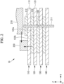
Fig. 2 is a longitudinal sectional view taken along the cutting line II-II illustrated inFig. 1 . - [
Fig. 3 ]
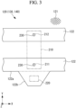
Fig. 3 is a plan view of a second layer substrate, a third layer substrate, or a fourth layer substrate of the circuit board structure according to one embodiment of the present disclosure. - [
Fig. 4 ]
Fig. 4 is a plan view of a second layer substrate, a third layer substrate, or a fourth layer substrate according to another example of the circuit board structure according to one embodiment of the present disclosure. - [
Fig. 5 ]
Fig. 5 is a plan view of a first layer substrate according to a modified example of the circuit board structure according one embodiment of the present disclosure. - [
Fig. 6 ]
Fig. 6 is a plan view of a first layer substrate according to a modified example of the circuit board structure according one embodiment of the present disclosure. - A circuit board structure and an electric compressor including the same according to one embodiment of the present disclosure will be described below with reference to the drawings.
- A
circuit board structure 10 is a part of an electronic device forming a control unit used for controlling driving of an electric compressor. Thus, thecircuit board structure 10 is provided in the electric compressor. - As illustrated in
Fig. 1 andFig. 2 , thecircuit board structure 10 is formed of a plurality of substrates laminated in the Z-axis direction and includes, for example, afirst layer substrate 110 and asecond layer substrate 120. Note that the number of substrates to be laminated can be changed as appropriate in accordance with the specification. - Further, an
electronic component 210 and atemperature sensor 220 are arranged on the front side (the top face in the Z-axis direction inFig. 2 ) of thefirst layer substrate 110. - The
electronic component 210 is a component that is electrically connected to patterns of each substrate described later and generates heat when current is supplied thereto. An example of theelectronic component 210 may be a capacitor. - The
temperature sensor 220 is a sensor that acquires the temperature of theelectronic component 210 and is arranged adjacent to theelectronic component 210. The expression of an object being "adjacent to" as used herein means a state where the object is not in contact with theelectronic component 210 and is arranged near theelectronic component 210 while maintaining a distance that can ensure electrical insulation between the object and theelectronic component 210 or afirst layer pattern 112 described later. An example of thetemperature sensor 220 may be a thermistor. - The
first layer substrate 110 has a firstinsulating layer 111 andfirst layer patterns 112. - The first
insulating layer 111 is a plate-like insulating component. - Each
first layer pattern 112 is a circuit with a conductor foil (for example, a copper foil) formed on the front side of the firstinsulating layer 111. In the case ofFig. 1 , twofirst layer patterns 112 are represented, and each first layer pattern has a width in the X direction and extends in the Y direction. - As illustrated in
Fig. 2 , thesecond layer substrate 120 is a substrate stacked on the backside (the bottom face in the Z-axis direction inFig. 2 ) of thefirst layer substrate 110. - As illustrated in
Fig. 2 andFig. 3 , thesecond layer substrate 120 has a secondinsulating layer 121 andsecond layer patterns 122. - The second
insulating layer 121 is a plate-like insulating component. - Each
second layer pattern 122 is a circuit with a conductor foil (for example, a copper foil) formed on the front side of the secondinsulating layer 121. In the case ofFig. 3 , twosecond layer patterns 122 are represented, and each second layer pattern has a width in the Y direction and extends in the X direction. Thesecond layer patterns 122 are located on the backside of the firstinsulating layer 111 in a state where thesecond layer substrate 120 is stacked on thefirst layer substrate 110. - One
second layer pattern 122 of the twosecond layer patterns 122 has a second layermain pattern part 122a and a second layer expandedpattern part 122b. - The second layer
main pattern part 122a is a portion having a width in the Y direction and extending in the X direction in the same manner as the othersecond layer pattern 122 and the first layer main pattern. - The second layer expanded
pattern part 122b is a portion formed so as to protrude from the edge along the Y direction of the second layermain pattern part 122a. Thus, it can be said that the second layer expandedpattern part 122b is a partially expanded portion of the edge along the Y direction of the second layermain pattern part 122a. Herein, the second layer expandedpattern part 122b is electrically/thermally connected to the second layermain pattern part 122a. - Note that, in
Fig. 2 andFig. 3 , boundaries illustrated by two-dot chain lines are depicted between the second layermain pattern part 122a and the second layer expandedpattern part 122b, but these boundaries are virtual lines for illustration. Further, in the case illustrated inFig. 3 , the second layer expandedpattern part 122b is formed so as to have a smaller area than the second layermain pattern part 122a. - A
lead terminal 211 and alead terminal 212 of theelectronic component 210 are electrically connected to thefirst layer patterns 112 and the second layer patterns 122 (the second layermain pattern part 122a) described above. Thus, theelectronic component 210 is mounted on thefirst layer pattern 112 and thesecond layer pattern 122. For example, thelead terminal 211 and thelead terminal 212 are inserted through and mounted on respective through-holes 230 penetrating through thefirst layer substrate 110 including thefirst layer patterns 112 and thesecond layer substrate 120 including thesecond layer patterns 122. - Note that any one of the
lead terminal 211 and thelead terminal 212 is the plus terminal, and the other is the minus terminal. - Further, it is apparent that the
first layer pattern 112 and thesecond layer pattern 122 electrically connected to the plus terminal of theelectronic component 210 are the plus patterns, and thefirst layer pattern 112 and thesecond layer pattern 122 electrically connected to the minus terminal of theelectronic component 210 are the minus patterns. - In the above configuration, as illustrated in
Fig. 2 andFig. 3 , the second layermain pattern part 122a is at a position overlapping with theelectronic component 210 in the XY direction when planarly viewed in the Z-axis direction. - This is natural in view of the
lead terminal 211 of theelectronic component 210 being connected to the second layermain pattern part 122a. - On the other hand, the second layer expanded
pattern part 122b is at a position overlapping with thetemperature sensor 220 in the XY direction when planarly viewed in the Z-axis direction. Thus, thetemperature sensor 220 is located right above in the Z-axis direction of the second layer expandedpattern part 122b. In other words, the second layer expandedpattern part 122b can be formed so as to include the region right under in the Z-axis direction of thetemperature sensor 220. In yet other words, the second layer expandedpattern part 122b can be formed by partially expanding the edge (contour) of the second layer main pattern part to surround thetemperature sensor 220 when planarly viewed in the Z-axis direction. - Note that the second layer expanded
pattern part 122b may be formed as illustrated inFig. 4 . - The second layer expanded
pattern part 122b formed as described above functions as follows. - As illustrated in
Fig. 2 , first, the heat of theelectronic component 210 is transferred to the second layermain pattern part 122a located right under in the Z-axis direction of theelectronic component 210. - Note that the heat is transferred via the
first layer pattern 112, the first insulatinglayer 111, thelead terminal 211, and the through-hole 230. - Next, the heat is transferred to the second layer expanded
pattern part 122b electrically/thermally connected to the second layermain pattern part 122a. - The heat is then transferred to the
temperature sensor 220 located right above in the Z-axis direction of the second layer expandedpattern part 122b. - Note that the heat is transferred via the first insulating
layer 111. - This makes it possible to realize heat transfer in the Z-axis direction by heat conduction via the second layer pattern 122 (see the dashed line arrow illustrated in
Fig. 2 ) in addition to heat transfer in the XY direction mainly by radiation above the first layer substrate 110 (see the two-dot chain line arrow illustrated inFig. 2 ). - Note that it is sufficient that the
temperature sensor 220 is at least arranged near theelectronic component 210, but it is preferable to arrange thetemperature sensor 220 on the straight line L passing through the two through-holes 230 as illustrated inFig. 1 in terms of efficiently receiving the heat of theelectronic component 210 by radiation. - Further, as with the
third layer substrate 130 and thefourth layer substrate 140 illustrated inFig. 2 , the n-th layer substrate having the same structure as thesecond layer substrate 120 may be laminated. Herein, n is an integer of three or greater, and the n-th layer substrate is stacked on the backside of the (n-1)-th layer substrate. - Further,
electronic components 210 may be installed at multiple positions on the front side of thefirst layer substrate 110. - Further, the expanded pattern part is not necessarily required to be formed on the substrates subsequent to the
third layer substrate 130. - According to the present embodiment, the following effects and advantages are achieved.
- The
second layer pattern 122 has the second layermain pattern part 122a overlapping with theelectronic component 210 when planarly viewed in the Z-axis direction and the second layer expandedpattern part 122b formed so as to overlap with thetemperature sensor 220 when planarly viewed in the Z-axis direction and connected to the second layermain pattern part 122a. Thus, thetemperature sensor 220 can acquire the temperature by radiation from the adjacentelectronic component 210 and by heat conduction via the second layer expandedpattern part 122b located right under thetemperature sensor 220. - Accordingly, the temperature closer to the true value can be acquired compared to a case where the temperature is acquired mainly by radiation from the
electronic component 210. - Further, the
first layer pattern 112 and the second layermain pattern part 122a are connected to each other via thelead terminal 211 of theelectronic component 210, and thus heat can be efficiently transferred from thefirst layer pattern 112, which is heated by theelectronic component 210, to the second layermain pattern part 122a. - Further, the
temperature sensor 220 is arranged on the straight line L passing through the two through-holes 230, and thus thetemperature sensor 220 can be arranged at a position near theelectronic component 210. - Accordingly, heat can be efficiently transferred from the
electronic component 210 to thetemperature sensor 220 by radiation. - As illustrated in
Fig. 5 , in thefirst layer substrate 110, thefirst layer pattern 112 may have asurrounding pattern part 112a. - The surrounding
pattern part 112a is a path using a conductor foil (for example, a copper foil) formed on the front side of the first insulatinglayer 111 and is formed so as to entirely surround thetemperature sensor 220 in the XY direction. - In such a case, the
wiring patterns 221 functioning as the power line and the signal line of thetemperature sensor 220 extend in the Z-axis direction via other through-holes or the like so that thewiring patterns 221 are not in contact with the surroundingpattern part 112a. - Note that the surrounding
pattern part 112a may be formed so as to partially surround thetemperature sensor 220 in the XY direction without entirely surrounding thetemperature sensor 220 as illustrated inFig. 6 . - With such a configuration, heat can be efficiently transferred from the
first layer pattern 112, which is heated by theelectronic component 210, to thetemperature sensor 220 via the surroundingpattern part 112a. - One embodiment described above is understood as follows, for example.
- The circuit board structure (10) according to a first aspect of the present disclosure includes: a first layer substrate (110) including a first insulating layer (111) and a first layer pattern (112) formed on the front side of the first insulating layer; a second layer substrate (120) including a second insulating layer (121) and a second layer pattern (122) formed on the front side of the second insulating layer, the second layer substrate being stacked on the first layer substrate such that the second layer pattern is located on the backside of the first insulating layer; a heat element (210) mounted on the first layer pattern and the second layer pattern; and a temperature acquisition unit (220) mounted on the first layer substrate at a position not in contact with and adjacent to the heat element and configured to acquire the temperature of the heat element, and the second layer pattern has a second layer main pattern part (122a) overlapping with the heat element when planarly viewed in a laminating direction of the first layer substrate and the second layer substrate, the heat element being mounted on the second layer main pattern part, and a second layer expanded pattern part (122b) formed so as to overlap with the temperature acquisition unit when planarly viewed in the laminating direction and connected to the second layer main pattern part.
- The circuit board structure includes: the first layer substrate; the second layer substrate stacked on the first layer substrate; the heat element mounted on the first layer pattern and the second layer pattern; and the temperature acquisition unit mounted on the first layer substrate at a position not in contact with and adjacent to the heat element and configured to acquire the temperature of the heat element, and the second layer pattern has the second layer main pattern part overlapping with the heat element when planarly viewed in a laminating direction of the first layer substrate and the second layer substrate and has the second layer expanded pattern part formed so as to overlap with the temperature acquisition unit when planarly viewed in the laminating direction and connected to the second layer main pattern part. Thus, the temperature acquisition unit can acquire the temperature by radiation from the adjacent heat element and by heat conduction via the second layer expanded pattern part of the second layer pattern located right under the temperature acquisition unit (in detail, also via the first insulating layer).
- Accordingly, the temperature closer to the true value can be acquired compared to a case where the temperature is acquired mainly by radiation from the heat element.
- An example of the heat element may be an electronic component such as a capacitor.
- An example of the temperature acquisition unit may be a temperature sensor such as a thermistor.
- Further, for the circuit board structure according toa second aspect of the present disclosure, which is dependent on the first aspect, the first layer pattern and the second layer main pattern part are connected to each other via a lead terminal (211) of the heat element.
- According to the circuit board structure of the present aspect, the first layer pattern and the second layer main pattern part are connected to each other via the lead terminal of the heat element, and thus heat can be efficiently transferred from the first layer pattern, which is heated by the heat element, to the second layer main pattern part.
- Further, for the circuit board structure according to a third aspect of the present disclosure, which is dependent on the first aspect or the second aspect, the first layer substrate has two through-holes (230) penetrating through the first layer pattern, and the temperature acquisition unit is arranged on a straight line (L) passing through the two through-holes.
- According to the circuit board structure of the present aspect, the first layer substrate has two through-holes penetrating through the first layer pattern, and the temperature acquisition unit is arranged on a straight line passing through the two through-holes. Thus, the temperature acquisition unit can be arranged at a position near the heat element.
- Accordingly, heat can be efficiently transferred from the heat element to the temperature acquisition unit by radiation.
- Further, for the circuit board structure according to a fourth aspect of the present disclosure, which is dependent on any one of the first aspect to the third aspect, when the circuit board structure includes an (n-1)-th layer substrate having an (n-1)-th insulating layer and an (n-1)-th layer pattern formed on the front side of the (n-1)-th insulating layer, the (n-1)-th layer substrate being stacked on an (n-2)-th layer substrate such that the (n-1)-th layer pattern is located on the backside of an (n-2)-th insulating layer, and where n is an integer of three or greater, the circuit board structure includes an n-th layer substrate having an n-th insulating layer and an n-th layer pattern formed on the front side of the n-th insulating layer, the n-th layer substrate being stacked on the (n-1)-th layer substrate such that the n-th layer pattern is located on the backside of the (n-1)-th insulating layer, the heat element is also mounted on the n-th layer pattern, and the n-th layer pattern has an n-th layer main pattern part overlapping with the heat element when planarly viewed in a laminating direction, the heat element being mounted on the n-th layer main pattern part, and an n-th layer expanded pattern part formed so as to overlap with the temperature acquisition unit when planarly viewed in the laminating direction and connected to the n-th layer main pattern part.
- According to the circuit board structure of the present aspect, the n-th layer pattern has the n-th layer expanded pattern part. Thus, even when the third layer substrate (130), the fourth layer substrate (140), ... are stacked on the second layer substrate, the temperature acquisition unit can acquire the temperature by heat conduction via each expanded pattern part.
- Further, for the circuit board structure according to a fifth aspect of the present disclosure, which is dependent on any one of the first aspect to the fourth aspect, the first layer pattern has a surrounding pattern part (112a) surrounding the temperature acquisition unit when planarly viewed in the laminating direction.
- According to the circuit board structure of the present aspect, the first layer pattern has a surrounding pattern part surrounding the temperature acquisition unit when planarly viewed in the laminating direction, and thus heat can be efficiently transferred from the first layer pattern, which is heated by the heat element, to the temperature acquisition unit via the surrounding pattern part.
- Further, the electric compressor according to a sixth aspect of the present disclosure includes the circuit board structure according to any one of the first aspect to the fifth aspect.
-
- 10 circuit board structure
- 110 first layer substrate
- 111 first insulating layer
- 112 first layer pattern
- 112a surrounding pattern part
- 120 second layer substrate
- 121 second insulating layer
- 122 second layer pattern
- 122a second layer main pattern part
- 122b second layer expanded pattern part
- 130 third layer substrate
- 140 fourth layer substrate
- 210 electronic component (heat element)
- 211 lead terminal
- 212 lead terminal
- 220 temperature sensor (temperature acquisition unit)
- 221 wiring pattern
- 230 through-hole
Claims (6)
- A circuit board structure comprising:a first layer substrate including a first insulating layer and a first layer pattern formed on a front side of the first insulating layer;a second layer substrate including a second insulating layer and a second layer pattern formed on a front side of the second insulating layer, the second layer substrate being stacked on the first layer substrate such that the second layer pattern is located on a backside of the first insulating layer;a heat element mounted on the first layer pattern and the second layer pattern; anda temperature acquisition unit mounted on the first layer substrate at a position not in contact with and adjacent to the heat element and configured to acquire a temperature of the heat element,wherein the second layer pattern includesa second layer main pattern part overlapping with the heat element when planarly viewed in a laminating direction of the first layer substrate and the second layer substrate, the heat element being mounted on the second layer main pattern part, anda second layer expanded pattern part formed so as to overlap with the temperature acquisition unit when planarly viewed in the laminating direction and connected to the second layer main pattern part.
- The circuit board structure according to claim 1, wherein the first layer pattern and the second layer main pattern part are connected to each other via a lead terminal of the heat element.
- The circuit board structure according to claim 1 or 2,wherein the first layer substrate includes two through-holes penetrating through the first layer pattern, andwherein the temperature acquisition unit is arranged on a straight line passing through the two through-holes.
- The circuit board structure according to claim 1 or 2, whereinwhen the circuit board structure comprises an (n-1)-th layer substrate including an (n-1)-th insulating layer and an (n-1)-th layer pattern formed on a front side of the (n-1)-th insulating layer, the (n-1)-th layer substrate being stacked on an (n-2)-th layer substrate such that the (n-1)-th layer pattern is located on a backside of an (n-2)-th insulating layer, and where n is an integer of three or greater,the circuit board further comprises an n-th layer substrate including an n-th insulating layer and an n-th layer pattern formed on a front side of the n-th insulating layer, the n-th layer substrate being stacked on the (n-1)-th layer substrate such that the n-th layer pattern is located on a backside of the (n-1)-th insulating layer,the heat element is also mounted on the n-th layer pattern, andthe n-th layer pattern includesan n-th layer main pattern part overlapping with the heat element when planarly viewed in the laminating direction, the heat element being mounted on the n-th layer main pattern part, andan n-th layer expanded pattern part formed so as to overlap with the temperature acquisition unit when planarly viewed in the laminating direction and connected to the n-th layer main pattern part.
- The circuit board structure according to claim 1 or 2, wherein the first layer pattern includes a surrounding pattern part surrounding the temperature acquisition unit when planarly viewed in the laminating direction.
- An electric compressor comprising the circuit board structure according to claim 1 or 2.
Applications Claiming Priority (2)
| Application Number | Priority Date | Filing Date | Title |
|---|---|---|---|
| JP2022064489A JP2023154870A (en) | 2022-04-08 | 2022-04-08 | Substrate structure and electric compressor equipped with the same |
| PCT/JP2023/009987 WO2023195311A1 (en) | 2022-04-08 | 2023-03-15 | Substrate structure and electric compressor having same |
Publications (2)
| Publication Number | Publication Date |
|---|---|
| EP4492925A1 true EP4492925A1 (en) | 2025-01-15 |
| EP4492925A4 EP4492925A4 (en) | 2025-06-18 |
Family
ID=88001153
Family Applications (1)
| Application Number | Title | Priority Date | Filing Date |
|---|---|---|---|
| EP23784603.5A Pending EP4492925A4 (en) | 2022-04-08 | 2023-03-15 | Substrate structure and electric compressor having same |
Country Status (5)
| Country | Link |
|---|---|
| US (1) | US20250247943A1 (en) |
| EP (1) | EP4492925A4 (en) |
| JP (1) | JP2023154870A (en) |
| CN (2) | CN219718576U (en) |
| WO (1) | WO2023195311A1 (en) |
Family Cites Families (6)
| Publication number | Priority date | Publication date | Assignee | Title |
|---|---|---|---|---|
| JP2005278344A (en) * | 2004-03-25 | 2005-10-06 | Denso Corp | Motor control device |
| JP5458966B2 (en) * | 2010-03-08 | 2014-04-02 | 日本電気株式会社 | Mounting structure of temperature detection element |
| JP2014116329A (en) | 2011-04-01 | 2014-06-26 | Sanyo Electric Co Ltd | Protection circuit module and battery pack |
| JP6119602B2 (en) * | 2013-12-26 | 2017-04-26 | 株式会社デンソー | Electronic equipment |
| JP6597420B2 (en) * | 2016-03-11 | 2019-10-30 | 日本精工株式会社 | Motor control device and electric power steering device equipped with the same |
| JP2020003268A (en) * | 2018-06-26 | 2020-01-09 | 株式会社オートネットワーク技術研究所 | Substrate structure |
-
2022
- 2022-04-08 JP JP2022064489A patent/JP2023154870A/en active Pending
-
2023
- 2023-03-15 CN CN202320492341.XU patent/CN219718576U/en active Active
- 2023-03-15 CN CN202380030444.7A patent/CN118947227A/en active Pending
- 2023-03-15 EP EP23784603.5A patent/EP4492925A4/en active Pending
- 2023-03-15 US US18/854,856 patent/US20250247943A1/en active Pending
- 2023-03-15 WO PCT/JP2023/009987 patent/WO2023195311A1/en not_active Ceased
Also Published As
| Publication number | Publication date |
|---|---|
| CN118947227A (en) | 2024-11-12 |
| EP4492925A4 (en) | 2025-06-18 |
| JP2023154870A (en) | 2023-10-20 |
| US20250247943A1 (en) | 2025-07-31 |
| CN219718576U (en) | 2023-09-19 |
| WO2023195311A1 (en) | 2023-10-12 |
Similar Documents
| Publication | Publication Date | Title |
|---|---|---|
| US10251261B2 (en) | Circuit structure | |
| EP1100294A3 (en) | Bus bar heat sink | |
| EP2215899B1 (en) | Junction box | |
| WO2002049104A3 (en) | Power module having improved transient thermal impedance | |
| US4313262A (en) | Molybdenum substrate thick film circuit | |
| KR100525936B1 (en) | Electronic control apparatus | |
| US7265983B2 (en) | Power unit comprising a heat sink, and assembly method | |
| US8004849B2 (en) | Control unit with flexible circuit board | |
| EP2117044A1 (en) | Printed circuit board and method of manufacuring the same | |
| EP2953437A1 (en) | Three-dimensional power distribution interconnect structure | |
| US20250247943A1 (en) | Circuit board structure and electric compressor including the same | |
| GB1407201A (en) | Printed electric wiring arrangements | |
| EP2635097B1 (en) | An electric and/or electronic circuit including a printed circuit board, a separate circuit board and a power connector | |
| US10129987B2 (en) | Circuit carrier and a method for producing a circuit carrier | |
| JP2007128929A (en) | Metal core substrate, manufacturing method thereof, and electrical junction box | |
| JPH04118984A (en) | Mounting structure for electronic component | |
| US10420255B2 (en) | Electronic control device | |
| EP2200408B1 (en) | Circuit board device, in particular for an electric power consuming device in a motor vehicle | |
| US10225926B2 (en) | Contact arrangement for a multi-layer circuit board | |
| US20250311105A1 (en) | Printed circuit board and electronic control device | |
| US20190174619A1 (en) | Circuit boards and method to manufacture circuit boards | |
| JP4073682B2 (en) | Electronic component with shield cap | |
| US6301120B1 (en) | Circuit board apparatus | |
| US20250311086A1 (en) | Printed circuit board and electronic control device | |
| JP2003283169A (en) | Laminated structure of multilayer flexible printed circuit board and multilayer flat cable, and electric junction box using this structure |
Legal Events
| Date | Code | Title | Description |
|---|---|---|---|
| STAA | Information on the status of an ep patent application or granted ep patent |
Free format text: STATUS: THE INTERNATIONAL PUBLICATION HAS BEEN MADE |
|
| PUAI | Public reference made under article 153(3) epc to a published international application that has entered the european phase |
Free format text: ORIGINAL CODE: 0009012 |
|
| STAA | Information on the status of an ep patent application or granted ep patent |
Free format text: STATUS: REQUEST FOR EXAMINATION WAS MADE |
|
| 17P | Request for examination filed |
Effective date: 20241007 |
|
| AK | Designated contracting states |
Kind code of ref document: A1 Designated state(s): AL AT BE BG CH CY CZ DE DK EE ES FI FR GB GR HR HU IE IS IT LI LT LU LV MC ME MK MT NL NO PL PT RO RS SE SI SK SM TR |
|
| A4 | Supplementary search report drawn up and despatched |
Effective date: 20250516 |
|
| RIC1 | Information provided on ipc code assigned before grant |
Ipc: G01K 7/22 20060101ALI20250512BHEP Ipc: G01K 1/16 20060101ALI20250512BHEP Ipc: F04B 49/06 20060101ALI20250512BHEP Ipc: F04B 39/00 20060101ALI20250512BHEP Ipc: F04B 35/04 20060101ALI20250512BHEP Ipc: H05K 1/02 20060101AFI20250512BHEP |
|
| DAV | Request for validation of the european patent (deleted) | ||
| DAX | Request for extension of the european patent (deleted) |