EP4492823A1 - Hearing device with multiple input multiple output dc-dc converter - Google Patents
Hearing device with multiple input multiple output dc-dc converter Download PDFInfo
- Publication number
- EP4492823A1 EP4492823A1 EP23184842.5A EP23184842A EP4492823A1 EP 4492823 A1 EP4492823 A1 EP 4492823A1 EP 23184842 A EP23184842 A EP 23184842A EP 4492823 A1 EP4492823 A1 EP 4492823A1
- Authority
- EP
- European Patent Office
- Prior art keywords
- voltage
- input
- hearing device
- output
- converter
- Prior art date
- Legal status (The legal status is an assumption and is not a legal conclusion. Google has not performed a legal analysis and makes no representation as to the accuracy of the status listed.)
- Pending
Links
Images



Classifications
-
- H—ELECTRICITY
- H04—ELECTRIC COMMUNICATION TECHNIQUE
- H04R—LOUDSPEAKERS, MICROPHONES, GRAMOPHONE PICK-UPS OR LIKE ACOUSTIC ELECTROMECHANICAL TRANSDUCERS; ELECTRIC HEARING AIDS; PUBLIC ADDRESS SYSTEMS
- H04R25/00—Electric hearing aids
- H04R25/40—Arrangements for obtaining a desired directivity characteristic
- H04R25/407—Circuits for combining signals of a plurality of transducers
-
- H—ELECTRICITY
- H04—ELECTRIC COMMUNICATION TECHNIQUE
- H04R—LOUDSPEAKERS, MICROPHONES, GRAMOPHONE PICK-UPS OR LIKE ACOUSTIC ELECTROMECHANICAL TRANSDUCERS; ELECTRIC HEARING AIDS; PUBLIC ADDRESS SYSTEMS
- H04R3/00—Circuits for transducers
-
- H—ELECTRICITY
- H02—GENERATION; CONVERSION OR DISTRIBUTION OF ELECTRIC POWER
- H02M—APPARATUS FOR CONVERSION BETWEEN AC AND AC, BETWEEN AC AND DC, OR BETWEEN DC AND DC, AND FOR USE WITH MAINS OR SIMILAR POWER SUPPLY SYSTEMS; CONVERSION OF DC OR AC INPUT POWER INTO SURGE OUTPUT POWER; CONTROL OR REGULATION THEREOF
- H02M1/00—Details of apparatus for conversion
- H02M1/0083—Converters characterised by their input or output configuration
- H02M1/009—Converters characterised by their input or output configuration having two or more independently controlled outputs
-
- H—ELECTRICITY
- H02—GENERATION; CONVERSION OR DISTRIBUTION OF ELECTRIC POWER
- H02M—APPARATUS FOR CONVERSION BETWEEN AC AND AC, BETWEEN AC AND DC, OR BETWEEN DC AND DC, AND FOR USE WITH MAINS OR SIMILAR POWER SUPPLY SYSTEMS; CONVERSION OF DC OR AC INPUT POWER INTO SURGE OUTPUT POWER; CONTROL OR REGULATION THEREOF
- H02M3/00—Conversion of DC power input into DC power output
- H02M3/02—Conversion of DC power input into DC power output without intermediate conversion into AC
- H02M3/04—Conversion of DC power input into DC power output without intermediate conversion into AC by static converters
- H02M3/06—Conversion of DC power input into DC power output without intermediate conversion into AC by static converters using resistors or capacitors, e.g. potential divider
- H02M3/07—Conversion of DC power input into DC power output without intermediate conversion into AC by static converters using resistors or capacitors, e.g. potential divider using capacitors charged and discharged alternately by semiconductor devices with control electrode, e.g. charge pumps
-
- H—ELECTRICITY
- H02—GENERATION; CONVERSION OR DISTRIBUTION OF ELECTRIC POWER
- H02M—APPARATUS FOR CONVERSION BETWEEN AC AND AC, BETWEEN AC AND DC, OR BETWEEN DC AND DC, AND FOR USE WITH MAINS OR SIMILAR POWER SUPPLY SYSTEMS; CONVERSION OF DC OR AC INPUT POWER INTO SURGE OUTPUT POWER; CONTROL OR REGULATION THEREOF
- H02M3/00—Conversion of DC power input into DC power output
- H02M3/02—Conversion of DC power input into DC power output without intermediate conversion into AC
- H02M3/04—Conversion of DC power input into DC power output without intermediate conversion into AC by static converters
- H02M3/06—Conversion of DC power input into DC power output without intermediate conversion into AC by static converters using resistors or capacitors, e.g. potential divider
- H02M3/07—Conversion of DC power input into DC power output without intermediate conversion into AC by static converters using resistors or capacitors, e.g. potential divider using capacitors charged and discharged alternately by semiconductor devices with control electrode, e.g. charge pumps
- H02M3/073—Charge pumps of the Schenkel-type
- H02M3/075—Charge pumps of the Schenkel-type including a plurality of stages and two sets of clock signals, one set for the odd and one set for the even numbered stages
-
- H—ELECTRICITY
- H04—ELECTRIC COMMUNICATION TECHNIQUE
- H04R—LOUDSPEAKERS, MICROPHONES, GRAMOPHONE PICK-UPS OR LIKE ACOUSTIC ELECTROMECHANICAL TRANSDUCERS; ELECTRIC HEARING AIDS; PUBLIC ADDRESS SYSTEMS
- H04R25/00—Electric hearing aids
- H04R25/60—Mounting or interconnection of hearing aid parts, e.g. inside tips, housings or to ossicles
- H04R25/602—Mounting or interconnection of hearing aid parts, e.g. inside tips, housings or to ossicles of batteries
-
- H—ELECTRICITY
- H04—ELECTRIC COMMUNICATION TECHNIQUE
- H04R—LOUDSPEAKERS, MICROPHONES, GRAMOPHONE PICK-UPS OR LIKE ACOUSTIC ELECTROMECHANICAL TRANSDUCERS; ELECTRIC HEARING AIDS; PUBLIC ADDRESS SYSTEMS
- H04R25/00—Electric hearing aids
- H04R25/60—Mounting or interconnection of hearing aid parts, e.g. inside tips, housings or to ossicles
- H04R25/609—Mounting or interconnection of hearing aid parts, e.g. inside tips, housings or to ossicles of circuitry
-
- H—ELECTRICITY
- H02—GENERATION; CONVERSION OR DISTRIBUTION OF ELECTRIC POWER
- H02M—APPARATUS FOR CONVERSION BETWEEN AC AND AC, BETWEEN AC AND DC, OR BETWEEN DC AND DC, AND FOR USE WITH MAINS OR SIMILAR POWER SUPPLY SYSTEMS; CONVERSION OF DC OR AC INPUT POWER INTO SURGE OUTPUT POWER; CONTROL OR REGULATION THEREOF
- H02M1/00—Details of apparatus for conversion
- H02M1/10—Arrangements incorporating converting means for enabling loads to be operated at will from different kinds of power supplies, e.g. from AC or DC
-
- H—ELECTRICITY
- H04—ELECTRIC COMMUNICATION TECHNIQUE
- H04R—LOUDSPEAKERS, MICROPHONES, GRAMOPHONE PICK-UPS OR LIKE ACOUSTIC ELECTROMECHANICAL TRANSDUCERS; ELECTRIC HEARING AIDS; PUBLIC ADDRESS SYSTEMS
- H04R1/00—Details of transducers, loudspeakers or microphones
- H04R1/10—Earpieces; Attachments therefor ; Earphones; Monophonic headphones
- H04R1/1025—Accumulators specially adapted for earpieces; Arrangements specially adapted for charging thereof
-
- H—ELECTRICITY
- H04—ELECTRIC COMMUNICATION TECHNIQUE
- H04R—LOUDSPEAKERS, MICROPHONES, GRAMOPHONE PICK-UPS OR LIKE ACOUSTIC ELECTROMECHANICAL TRANSDUCERS; ELECTRIC HEARING AIDS; PUBLIC ADDRESS SYSTEMS
- H04R2225/00—Details of deaf aids covered by H04R25/00, not provided for in any of its subgroups
- H04R2225/31—Aspects of the use of accumulators in hearing aids, e.g. rechargeable batteries or fuel cells
-
- H—ELECTRICITY
- H04—ELECTRIC COMMUNICATION TECHNIQUE
- H04R—LOUDSPEAKERS, MICROPHONES, GRAMOPHONE PICK-UPS OR LIKE ACOUSTIC ELECTROMECHANICAL TRANSDUCERS; ELECTRIC HEARING AIDS; PUBLIC ADDRESS SYSTEMS
- H04R2225/00—Details of deaf aids covered by H04R25/00, not provided for in any of its subgroups
- H04R2225/33—Aspects relating to adaptation of the battery voltage, e.g. its regulation, increase or decrease
-
- H—ELECTRICITY
- H04—ELECTRIC COMMUNICATION TECHNIQUE
- H04R—LOUDSPEAKERS, MICROPHONES, GRAMOPHONE PICK-UPS OR LIKE ACOUSTIC ELECTROMECHANICAL TRANSDUCERS; ELECTRIC HEARING AIDS; PUBLIC ADDRESS SYSTEMS
- H04R2225/00—Details of deaf aids covered by H04R25/00, not provided for in any of its subgroups
- H04R2225/57—Aspects of electrical interconnection between hearing aid parts
-
- H—ELECTRICITY
- H04—ELECTRIC COMMUNICATION TECHNIQUE
- H04R—LOUDSPEAKERS, MICROPHONES, GRAMOPHONE PICK-UPS OR LIKE ACOUSTIC ELECTROMECHANICAL TRANSDUCERS; ELECTRIC HEARING AIDS; PUBLIC ADDRESS SYSTEMS
- H04R25/00—Electric hearing aids
- H04R25/02—Electric hearing aids adapted to be supported entirely by ear
Definitions
- the present disclosure relates to a hearing device comprising a multiple input multiple output, MIMO, switched capacitor, SC, DC-DC converter.
- Modern hearing devices comprise chipsets that incorporate a wide variety of switched capacitor, SC, DC-DC power converters to provide efficient voltage conversion from the input voltage levels of their power units, e.g., lithium-ion batteries, which typically provide a battery cell voltage in the range from ⁇ 4,2 V to ⁇ 2,8 V depending on the battery's state of charge, and down to lower voltages.
- SC switched capacitor
- This downconversion is crucial in ensuring a long-lasting source of power while enabling increasingly power-demanding functions in the hearing device.
- Many hearing devices utilize multiple voltage levels below that of the input voltage level in order to minimize power consumption. To provide these supply voltages, hearing devices have been provided with multiple SC DC-DC converters in addition to several linear regulators, each of which degrades the power conversion efficiency.
- SC converters further requires a large amount of off-chip multilayer ceramic capacitors. This increases the printed circuit board area, and consequently the total volume of the electronics, which can be an issue, especially for miniature devices such as hearing aids and ear buds.
- SC converter topologies require high-voltage, HV, power switches and therefore a process with HV transistors which may limit their integrability in modern low-voltage integrated circuit, IC, process nodes and require dedicated HV processes or additional process options.
- SC converters are electromagnetic interference, EMI, aggressors with varying switching frequencies, pulse widths and/or pulse densities, which means that careful switching frequency/load current planning is required to avoid interference in adjacent radio systems.
- EP 3 447 894 B1 relates to a head-wearable hearing device comprising a multiple-output switched capacitor DC-DC converter.
- Said multiple-output switched capacitor DC-DC converter comprises a switch matrix comprising a plurality of individually controllable semiconductor switches and a plurality of flying capacitors connected between respective sets of circuit nodes of the switch matrix.
- a controller is connected to respective control terminals of the plurality of individually controllable semiconductor switches of the switch matrix to configure first and second converter sections to form first and second converter topologies, respectively, based on a topology selection rule.
- this disclosure does not support multiple input voltages and only provides a single output voltage at a time depending on the configuration of the SC DC-DC converter circuit.
- the invention achieves this by a hearing device configured to be worn at an ear of a user.
- the hearing device comprises an input transducer adapted for capturing sound and providing a microphone input transducer signal based on the captured sound.
- the hearing device comprises a signal processing unit adapted for processing the input transducer signal and providing an output signal based on the processed input transducer signal.
- the hearing device comprises an output transducer adapted for providing a stimulation output signal based on the output signal.
- the hearing device comprises a battery configured for providing a battery cell voltage.
- the hearing device comprises a multiple input multiple output, MIMO, switched capacitor, SC, DC-DC converter coupled to the battery.
- the MIMO SC DC-DC converter comprises two or more inputs, each adapted for receiving a voltage input.
- the MIMO SC DC-DC converter comprises two or more outputs, each adapted for providing a voltage output of a different voltage from the other outputs. At least two of the two or more outputs can provide a voltage output simultaneously.
- the MIMO SC DC-DC converter is configured for converting each voltage input to a voltage output of a different voltage.
- the MIMO SC DC-DC converter comprises multiple inputs configured for receiving different input voltages as this allows the hearing MIMO SC DC-DC converter to maintain efficient power conversion and supply of power, even during use as the battery is depleted and the battery cell voltage drops, as the battery may be coupled to the input configured for receiving the voltage input closest to the current battery cell voltage.
- the disclosed MIMO SC DC-DC converter can replace multiple current SC converters in existing hearing devices while providing higher conversion efficiencies to more voltage levels.
- the converter can make use of an integrated voltage input demultiplexer, which allows efficient conversion across a battery's, e.g., lithium-ion, discharge cycle.
- a battery's e.g., lithium-ion, discharge cycle.
- the battery should merely be routed to another voltage input, corresponding to a minimal product change.
- MIMO SC DC-DC converter is slightly more complex during start-up than some of the existing series-parallel converters, the overall system complexity is reduced by replacing multiple converters by one MIMO SC DC-DC converter. This also applies to EMI issues, which current SC converters often are associated with.
- the disclosed MIMO SC DC-DC converter's power switches can occupy an area of less than 0,5 mm 2 . This is because they can be implemented as highly efficient thin-oxide devices in semiconductor process nodes suitable for the hearing device's signal processing unit's chip. Often SC converters are implemented in more mature process node along with EMI- and noise-sensitive analog circuitry like analog-to-digital converters or radios. By moving the SC converter to an inherently noise-immune chip, it is possible to remove noisy switching regulators from the sensitive circuit types. The disclosed MIMO SC DC-DC converter can thus help enable a hearing device solution with a higher level of integration and fewer integrated circuits in the product.
- One or more first electronic component(s) of the hearing device is/are coupled to a first output of the two or more outputs and one or more second electronic component(s) of the hearing device is/are coupled to a second output of the two or more outputs.
- any of the named components e.g., the microphone, the signal processing unit, and the output transducer, may be comprised in the one or more first electronic component(s) or in the one or more second electronic component(s).
- low and high voltage depends on context.
- high and low voltages are used in the context of micro electronic devices and are used relative to each other.
- differences between high voltage and low voltage might be less than 1 V, a voltage difference that can be a lot for certain transistor types to handle, in contrast to other fields of electrical engineering or a layman's definition which would categorize high voltage as starting around 1000-1500V depending on whether AC or DC voltage is used.
- a voltage output is an output from which an output current may be drawn.
- the current flowing out of the output voltage node may be positive or zero.
- the current flowing out of an output node may also be negative, as for example when the output node is used as an input node.
- the hearing device is configured to be worn by a user.
- the hearing device may be arranged at the user's ear, on the user's ear, over the user's ear, in the user's ear, in the user's ear canal, behind the user's ear and/or in the user's concha, i.e., the hearing device is configured to be worn in, on, over and/or at the user's ear.
- the user may wear two hearing devices, one hearing device at each ear.
- the two hearing devices may be connected, such as wirelessly connected and/or connected by wires, such as a binaural hearing aid system.
- the hearing device may be a hearable such as a headset, headphone, earphone, earbud, hearing aid, a personal sound amplification product, PSAP, an over-the-counter, OTC, hearing device, a hearing protection device, a one-size-fits-all hearing device, a custom hearing device or another head-wearable hearing device.
- Hearing devices can include both prescription devices and non-prescription devices.
- the hearing device may be embodied in various housing styles or form factors. Some of these form factors are Behind-the-Ear, BTE, hearing device, Receiver-in-Canal, RIC, hearing device, Receiver-in-Ear, RIE, also known as RITE, hearing device or Microphone-and-Receiver-in-Ear, MaRIE, hearing device.
- BTE Back-the-Ear
- hearing device Receiver-in-Canal
- RIC hearing device
- Receiver-in-Ear also known as RITE
- hearing device or Microphone-and-Receiver-in-Ear, MaRIE hearing device.
- These devices may comprise a BTE unit configured to be worn behind the ear of the user and an in the ear, ITE, unit configured to be inserted partly or fully into the user's ear canal.
- the BTE unit may comprise at least one input transducer, a battery and a processing unit.
- BTE hearing device refers to a hearing device where the receiver, i.e.
- the output transducer is comprised in the BTE unit and sound is guided to the ITE unit via a sound tube connecting the BTE and ITE units
- the terms RIE, RIC and MaRIE hearing devices refer to hearing devices where the receiver may be comprise in the ITE unit, which is coupled to the BTE unit via a connector cable or wire configured for transferring electric signals between the BTE and ITE units.
- Some of these form factors are In-the-Ear, ITE, hearing device, Completely-in-Canal, CIC, hearing device or Invisible-in-Canal, IIC, hearing device.
- These hearing devices may comprise an ITE unit, wherein the ITE unit may comprise at least one input transducer, a battery, a processing unit and an output transducer.
- These form factors may be custom devices, meaning that the ITE unit may comprise a housing having a shell made from a hard material, such as a hard polymer or metal, or a soft material such as a rubber-like polymer, molded to have an outer shape conforming to the shape of the specific user's ear canal.
- earbuds on the ear headphones or over the ear headphones.
- the person skilled in the art is well aware of different kinds of hearing devices and of different options for arranging the hearing device in, on, over and/or at the ear of the hearing device wearer.
- the hearing device (or pair of hearing devices) may be custom fitted, standard fitted, open fitted and/or occlusive fitted.
- the hearing device may comprise one or more input transducers, e.g., microphones.
- the one or more input transducers may comprise one or more microphones.
- the one or more input transducers may comprise one or more vibration sensors configured for detecting bone vibration.
- the one or more input transducer(s) may be configured for converting an acoustic signal into a first electric input signal.
- the first electric input signal may be an analogue signal.
- the first electric input signal may be a digital signal.
- the one or more input transducer(s) may be coupled to one or more analogue-to-digital converter(s) configured for converting the analogue first input signal into a digital first input signal.
- the hearing device may comprise one or more antenna(s) configured for wireless communication.
- the one or more antenna(s) may comprise an electric antenna.
- the electric antenna may be configured for wireless communication at a first frequency.
- the first frequency may be above 800 MHz, preferably a wavelength between 900 MHz and 6 GHz.
- the first frequency may be 902 MHz to 928 MHz.
- the first frequency may be 2,4 to 2,5 GHz.
- the first frequency may be 5,725 GHz to 5,875 GHz.
- the one or more antenna(s) may comprise a magnetic antenna.
- the magnetic antenna may comprise a magnetic core.
- the magnetic antenna may comprise a coil.
- the coil may be coiled around the magnetic core.
- the magnetic antenna may be configured for wireless communication at a second frequency.
- the second frequency may be below 100 MHz.
- the second frequency may be between 9 MHz and 15 MHz.
- the hearing device may comprise one or more wireless communication unit(s).
- the one or more wireless communication unit(s) may comprise one or more wireless receiver(s), one or more wireless transmitter(s), one or more transmitter-receiver pair(s) and/or one or more transceiver(s). At least one of the one or more wireless communication unit(s) may be coupled to the one or more antenna(s).
- the wireless communication unit may be configured for converting a wireless signal received by at least one of the one or more antenna(s) into a second electric input signal.
- the hearing device may be configured for wired/wireless audio communication, e.g., enabling the user to listen to media, such as music or radio and/or enabling the user to perform phone calls.
- the wireless signal may originate from one or more external source(s) and/or external devices, such as spouse microphone device(s), wireless audio transmitter(s), smart computer(s) and/or distributed microphone array(s) associated with a wireless transmitter.
- the wireless input signal(s) may origin from another hearing device, e.g., as part of a binaural hearing system and/or from one or more accessory device(s), such as a smartphone and/or a smart watch.
- the hearing device may include a processing unit.
- the processing unit may be configured for processing the first and/or second electric input signal(s).
- the processing may comprise compensating for a hearing loss of the user, i.e., apply frequency dependent gain to input signals in accordance with the user's frequency dependent hearing impairment.
- the processing may comprise performing feedback cancelation, beamforming, tinnitus reduction/masking, noise reduction, noise cancellation, speech recognition, bass adjustment, treble adjustment and/or processing of user input.
- the processing unit may be a processor, an integrated circuit, an application, functional module, etc.
- the processing unit may be implemented in a signal-processing chip or a printed circuit board, PCB.
- the processing unit may be configured to provide a first electric output signal based on the processing of the first and/or second electric input signal(s).
- the processing unit may be configured to provide a second electric output signal.
- the second electric output signal may be based on the processing of the first and/or second electric input signal(s).
- the hearing device may comprise an output transducer.
- the output transducer may be coupled to the processing unit.
- the output transducer may be a receiver. It is noted that in this context, a receiver may be a loudspeaker, whereas a wireless receiver may be a device configured for processing a wireless signal. The receiver may be configured for converting the first electric output signal into an acoustic output signal.
- the output transducer may be coupled to the processing unit via the magnetic antenna.
- the output transducer may be comprised in an ITE unit or in an earpiece, e.g., for Receiver-in-Ear (RIE) unit or Microphone-and-Receiver-in-Ear (MaRIE) unit, of the hearing device.
- RIE Receiver-in-Ear
- MaRIE Microphone-and-Receiver-in-Ear
- the battery may be a rechargeable battery, e.g., a Li-lon battery.
- the battery may be a replaceable battery.
- the hearing device may comprise a power management unit.
- the battery may be coupled to a charging coil configured for wireless recharging of the battery.
- the charging coil may be provided by the magnetic antenna.
- the battery may be a non-rechargeable battery, e.g., a ZnO battery.
- the hearing device may comprise a memory, including volatile and non-volatile forms of memory.
- the voltage input may be the battery cell voltage.
- the hearing device may further comprise an input power de-multiplexer comprising:
- the input power de-multiplexer may comprise one or more further de-multiplexer outputs, each coupled to a different input of the two or more inputs.
- the battery may be coupled to the MIMO SC DC-DC converter in a manner that allows for efficient switching between inputs. This is particularly advantageous as the battery runs through its discharge cycle, as the de-multiplexer may channel the battery cell voltage to the input of the of the two or more inputs that is best suited for handling the current battery cell voltage.
- the MIMO SC DC-DC converter may comprise multiple voltage stages, each voltage stage comprising:
- the first switch may be a controllable semiconductor switch, e.g., a transistor.
- the first switch may comprise:
- the second switch may be a controllable semiconductor switch, e.g., a transistor.
- the second switch may comprise:
- the terminology primary may be used instead of “upper”, e.g., the upper flying capacitor terminal may also be denoted as the primary flying capacitor terminal, and the terminology secondary may be used instead of “lower”, e.g., lower second capacitor terminal may also be denoted as the secondary second capacitor terminal.
- the voltage stages may be coupled together so that each voltage stage below the highest voltage stage comprises:
- highest voltage stage is used to denote the voltage stage configured for handling the highest voltage amongst the voltage stages.
- the first switches may be controlled by a first clock signal and the second switches may be controlled by a second clock signal, wherein the first and second clock signals are non-overlapping.
- the non-overlapping clock signals ensure that the first and second clock signals never cause their associated first and second switches to be closed (conductive, in a low-ohmic state) at the same time as to prevent cross-conduction.
- the first switches and the second switches thus alternate between the first switches being closed while the second switches are open and the first switches being open while the second switches are closed.
- the term "closed” is used for switches that are "on”, meaning that the provide a low-ohmic electrical path between their primary and secondary terminals.
- the term “open” is used for switches that are "off”, meaning that they do not provide a low-ohmic electrical path between their primary and secondary terminals.
- the first and second clock signals may comprise a first phase, in which the first switches are closed, and the second switches are open, and second phase, in which the first switches are open and the second switches are closed, wherein the first and second phases are separated in time by a pause duration, in which both the first switches and the second switches are open. This ensures that the first and second switches are never closed at the same time, which would lead to cross-conduction and potentially cause damage to the MIMO SC DC-DC converter and/or connected systems.
- One or more of the voltage stages may comprise an input of the two or more inputs and/or and output of the two or more outputs.
- the MIMO SC DC-DC converter may comprise five to ten voltage stages.
- the MIMO SC DC-DC converter may have a ladder topology, e.g., an asymmetric ladder topology. Each voltage stage below the highest voltage stage may be configured so that:
- the MIMO SC DC-DC may comprise a bootstrap capacitor and/or a bootstrap diode arranged to connect the flying capacitor of the highest voltage stage to the input of the two or more inputs that is configured for receiving the highest voltage input. It is advantageous to include a bootstrap capacitor and/or a bootstrap diode as this makes start-up of the MIMO SC DC-DC easier and provides a voltage level above the input voltage level to efficiently drive N-type transistors.
- the MIMO SC DC-DC may comprise a third capacitor coupled to the input of the two or more inputs that is configured for receiving the highest voltage input and to the input of the two or more inputs that is configured for receiving the second highest voltage input.
- the third capacitor is arranged between the input of the two or more inputs that is configured for receiving the highest voltage input and the input of the two or more inputs that is configured for receiving the second highest voltage input.
- the signal processing unit may be comprised by a signal processing chip, and the MIMO SC DC-DC converter may be integrated or co-integrated in the signal processing chip.
- the MIMO SC DC-DC converter When the MIMO SC DC-DC converter is co-integrated in the signal processing chip, one or more of the flying capacitors and/or one or more of the second capacitors may be implemented outside the signal processing chip, for example as discrete multilayer ceramic capacitors or capacitors integrated in a silicon interposer.
- the MIMO SC DC-DC converter is co-integrated in the signal processing chip, one or more of the first switches and/or one or more of the second switches may be implemented in the signal processing chip.
- the first switches and/or the second switches may be integrated metal-oxide-semiconductor field effect transistors, MOSFETs.
- the flying capacitors, the second capacitors, the third capacitor, and/or the bootstrap capacitor may be integrated metal-oxide-semiconductor, MOS, capacitors, metal-oxide-metal, MOM, capacitors, metal-insulator-metal, MIM, capacitors, or (deep) trench capacitors.
- each output may depend on the voltage level of the voltage input and/or which input is provided with the voltage input.
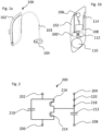
- Fig. 1a shows a hearing device 100, which in the shown embodiment is a RIE- or MaRie-type hearing aid.
- the hearing device 100 comprises a BTE component 102 adapted to be worn behind the ear of the user and an ITE component 104 adapted to be worn in the ear of the user.
- the hearing device comprises one or more input transducers 106, e.g., one or more microphones and/or one or more bone vibration sensors, configured for capturing sound in ambient air or through vibrations in the user's body respectively.
- the one or more input transducers may be arranged in the BTE component 102 and/or in the ITE component 104.
- the hearing device 100 comprises at least one output transducer, e.g., a loudspeaker, which in the shown embodiment is arranged in the ITE component 104, but which may alternatively be arranged in the BTE component 102.
- the BTE component 102 and the ITE component 104 are coupled by a connector 103 which comprises one or more electrically conducting wires for transferring electric signals between the BTE component 102 and the ITE component 104.
- the connector 103 comprises a hollow core for providing a fluid connection to the ITE component 104 for sound generated by the output transducer to be guided to the ear.
- Fig. 1b shows a schematic view of the BTE component 102 of the hearing device 100 shown in Fig. 1a .
- the BTE component 102 comprises an input transducer 106 in the form of a microphone.
- the input transducer 106 is coupled to a signal processing unit 108 adapted to process the signals representing the sound captured by the input transducer 106.
- the BTE component 102 comprises an electrical interface 114 configured for being connected to the connector 103 and therethrough to the ITE component 104. Through the electrical interface 114, the signal processing unit 108 is connected to the output transducer, whereby processed signals may be sent to the output transducer and converted into an acoustic output.
- the hearing device 100 further comprises a battery 110, preferably a rechargeable battery, e.g., a Li-lon battery.
- the battery can supply a battery cell voltage, e.g., 4,2V when at full capacity. As the battery 110 goes through its discharge cycle the battery cell voltage will drop whereby the battery 110 will supply a reduced battery cell voltage.
- the battery 110 is connected to an input power de-multiplexer 112 configured for receiving the battery cell voltage, and depending on the current battery cell voltage, route the battery cell voltage to a suitable input of a MIMO SC DC-DC converter 300.
- the MIMO SC DC-DC converter 300 comprises multiple inputs, each configured for receiving a voltage input.
- the MIMO SC DC-DC converter 300 may thus receive the battery cell voltage at one of the inputs, and convert the battery cell voltage, e.g., step up or step down, whereby the outputs may provide a voltage output that depends on the voltage level of the voltage input and which input the voltage input is supplied to.
- the MIMO SC DC-DC converter 300 is configured for converting the battery cell voltage received at one of the inputs to multiple voltage outputs with different voltages and provide the voltage outputs from respective outputs.
- the different electronic components of the hearing device 100 may thus be supplied with power from the output of the MIMO SC DC-DC converter 300 that provides the output voltages closest to the voltage the respective electronic component is configured to operate at. Examples of the MIMO SC DC-DC converter 300 and the voltage stages 200 will be disclosed in detail below.
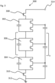
- Fig. 2 shows an example of a voltage stage 200 comprised by the MIMO SC DC-DC converter 300.
- the voltage stage 200 comprises a first upper connection node 202 and a second upper connection node 204 for connecting the voltage stage 200 to another voltage stage 200 in a higher voltage domain and/or to an input 218 of the multiple inputs.
- the voltage stage 200 comprises a first lower connection node 206 and a second lower connection node 208 for connecting the voltage stage 200 to another voltage stage 200 in a lower voltage domain and/or to a ground connection 312.
- the voltage stage 200 comprises a flying capacitor 210 with an upper flying capacitor terminal connected to the first upper connection node 202, and a lower flying capacitor terminal connected to the first lower connection node 206.
- the voltage stage 200 comprises a second capacitor 212 with an upper second capacitor terminal galvanically connected to the second upper connection node 204, and a lower second capacitor terminal connected to the second lower connection node 208.
- the voltage stage 200 comprises a first switch 214 with a lower first switch terminal galvanically connected to the first lower connection node 206 and the lower flying capacitor terminal, and an upper first switch terminal galvanically connected to the second upper connection node 204 and the upper second capacitor terminal.
- the voltage stage 200 comprises a second switch 216 with an upper second switch terminal galvanically connected to the first upper connection node 202 and the upper flying capacitor terminal, and a lower second switch terminal galvanically connected to the first upper connection node 204, the upper first switch terminal, and the upper second capacitor terminal.
- the second switch 216 is adapted for selectively providing a low-ohmic electrical connection between the upper flying capacitor terminal and the upper second capacitor terminal
- the first switch 214 is adapted for selectively providing a low-ohmic electrical connection between the lower flying capacitor terminal and the upper second capacitor terminal.
- Each of the first switch 214 and the second switch 216 are preferably provided by a controllable semiconductor switch, such as a transistor.
- Each of the first switch 214 and the second switch 216 may advantageously be implemented in fully-depleted silicon-on-insulator, FDSOI, semiconductor processes.
- the first switch 214 is controlled by a first clock signal cp
- the second switch 216 is controlled by a second clock signal ⁇ 2 .
- the first and second clock signals ⁇ 1 , ⁇ 2 are complimentary, meaning that they control the first and second switches 214, 216 so that the first switch 214 and the second switch 216 are never closed at the same time.
- the first and second clock signals ⁇ 1 , ⁇ 2 are separated by a pause duration 506 between opening the first switch 214 and closing the second switch 216 and between closing the first switch 214 and opening the second switch 216, in which pause duration 506 both the first switch 214 and the second switch 216 are open, i.e., off.
- the clock signals are said to be non-overlapping.
- the voltage stage 200 may comprise an input node 218 providing an input of the one or more inputs.
- the input node 218 can be coupled to the battery 110, e.g., via the input power de-multiplexer 112, so that the input node 218 can receive a voltage input.
- the voltage stage 200 may comprise an output node 220 providing an output of the one or more outputs.
- the output node 220 can be coupled to electronic components of the hearing device 100 that are configured for running on the voltage provided by that output node 220.
- Fig. 3 shows an example of the MIMO SC DC-DC converter 300 comprising multiple voltage stages 200 as described for Fig. 2 .
- the MIMO SC DC-DC converter 300 comprises a highest voltage stage 302, i.e., the voltage stage 200 amongst the multiple voltage stages that is configured to be in the highest voltage domain amongst the multiple voltage stages.
- the MIMO SC DC-DC converter 300 comprises a lowest voltage stage 304, i.e., the voltage stage 200 amongst the multiple voltage stages that is configured to be in the lowest voltage domain amongst the multiple voltage stages.
- the MIMO SC DC-DC converter 300 comprises n middle voltage stage(s) 306, where n is a positive integer or 0.
- the voltage stages 302, 304, 306 are connected, so that a respective voltage stage will be connected to its adjacent upper voltage stage through a connection of its first upper connection node 202 to the adjacent upper voltage stage's first lower connection node 206 and a connection of its second upper connection node 204 to the adjacent upper voltage stage's second lower connection node 208.
- the first upper connection node 202 is connected to a highest input node 314, i.e., the input of the two or more inputs that is configured for receiving the highest voltage.
- the first upper connection node 202 is connected to the highest input node 314 via a first switch 308.
- the second upper connection node 204 is left un-connected.
- a respective voltage stage will be connected to its adjacent lower voltage stage through a connection of its first lower connection node 206 to the adjacent lower voltage stage's first upper connection node 202 and a connection of its second lower connection node 206 to the adjacent lower voltage stage's second upper connection node 204.
- the first and second lower connection nodes 206, 208 are connected to ground 312.
- the first lower connection node 206 is connected to ground via a second switch 310 whereas the second lower connection node 208 is directly connected to ground 312.
- the MIMO SC DC-DC converter 300 has a ladder topology that allow a voltage output for each voltage stage 200. Additionally, these multiple voltage outputs are simultaneously available, meaning that all voltage outputs are available at the same time.
- the voltage level of respective voltage stage 200 is not constant but will vary depending on the voltage input and to which voltage stage the voltage input is applied. This also means that the shown MIMO SC DC-DC converter 300 has more possible output voltages than the number of voltage stages, as the voltage output of a voltage stage may be changed by controlling the voltage level of the voltage input and/or the voltage stage to which the voltage input is applied.
- Fig. 4 illustrates a further development of the MIMO SC DC-DC converter 300 shown in Fig. 3 .
- This MIMO SC DC-DC converter 300 further comprises a third capacitor 320 arranged between and connecting the highest input 314 and the second upper connection node 204 of the highest voltage stage 302. It is advantageous to include the third capacitor 320 as it enables the MIMO SC DC-DC converter 300 to perform step-up conversion of a voltage input applied to a lower voltage stage up to the voltage level of the highest input 314, which may thereby also act as an output.
- the MIMO SC DC-DC converter 300 also comprises a bootstrap diode 316 and a bootstrap capacitor 318 arranged between the first upper connection node 202 of the highest voltage stage 302 and the highest voltage node 314.
- the bootstrap diode 316 and the bootstrap capacitor 318 are arranged in series with each other, and the two are arranged in parallel with the first switch 308 that connects the first upper connection node 202 of the highest voltage stage 302 and the highest voltage node 314.
- the bootstrap diode 316 and the bootstrap capacitor 318 are advantageous as they make the startup of the MIMO SC DC-DC converter 300 easier.
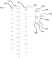
- Fig. 5 shows an example of the MIMO SC DC-DC converter 300 of Fig. 4 , where n is 3 so that the MIMO SC DC-DC converter 300 comprises 5 voltage stages 200, i.e., a highest voltage stage 302, a lowest voltage stage 304, and three middle voltage stages 306.
- the shown MIMO SC DC-DC converter 300 also comprises the third capacitor 320 to enable step-up conversion and a bootstrap diode 316 and a bootstrap capacitor 318 to facilitate startup.
- the first switches (S even ) are controlled by a first clock signal ⁇ 1
- the second switches (S odd ) are controlled by a second clock signal ⁇ 2 .
- the MIMO SC DC-DC converter 300 comprises 6 voltage nodes, i.e., one for each voltage stage and the highest input node 314, which may be used as inputs and/or outputs.
- the voltage nodes are denoted V o1 , V o2 , V o3 , V o4 , V o5 , and V o6 , where the o is short for output, although it may also be used for input, and the number 1-6 denotes the number of the voltage node counted from the lowest voltage stage 304 upwards.
- the MIMO SC DC-DC converter 300 comprises an input power de-multiplexer 112, 400, also denoted Batmux, which selectively connects the battery 110 to at least some of the inputs, i.e., routes the input voltage to a selected one of the inputs.
- the input power de-multiplexer 112, 400 comprises a de-multiplexer input 402 coupled to the battery 110 for receiving the battery cell voltage.
- the input power de-multiplexer 112, 400 also comprises a first de-multiplexer output 404 coupled to the highest input node 314, V o6 , a second de-multiplexer output 406 coupled to the input node of the highest voltage stage, V o5 , and a third de-multiplexer output 408 coupled to the input node of the voltage stage below the highest voltage stage, V o4 .
- the input power de-multiplexer 112, 400 may comprise fewer or more de-multiplexer outputs and/or the de-multiplexer outputs may be coupled to other voltage inputs. It is noted the input power de-multiplexer 112, 400 is controlled to select one of the de-multiplexer outputs at a time so that only one input receives an input voltage at any given time.
- the input power de-multiplexer 112, 400 may route the battery cell voltage to the desired input of the MIMO SC DC-DC converter 300, thereby providing the voltage input for conversion.
- the input power de-multiplexer 112, 400 comprises one or more control ports 410, 412 which can be coupled to the signal processing unit 108 or a dedicated control circuit. Through the control port(s) 410, 412, the input power de-multiplexer 112, 400 may be controlled to set which of the de-multiplexer outputs 404, 406, 408 should be used, and thus also which of the inputs of the MIMO SC DC-DC converter 300 should receive the voltage input.
- the voltage at the voltage nodes V o1 , V o2 , V o3 , V o4 , V o5 , and V o6 will depend on the level of the voltage input, and which input the input power de-multiplexer 112, 400 provides with the voltage input according to eq. 1.
- Table 1 below show the voltage level of the voltage output provided by each voltage node depending on the voltage level of the voltage input applied to the highest input node 314, V o6 .
- the battery is provided by a Li-lon battery, which can provide a battery cell voltage of 4,2 V when fully charged.
- a Li-lon battery which can provide a battery cell voltage of 4,2 V when fully charged.
- each of the electrical components of the hearing device 100 are configured for running on their respective optimal voltages, they may run on a voltage deviating from this if the provided voltage is not so high that it damages the electrical components or so low that it cannot power the respective component.
- linear low dropout regulators may be used to alleviate issues with too high voltages if desired.
- the voltage input may simply be applied to another of the input nodes.
- Tables 2 and 3 below shows the voltage outputs available when the voltage input is applied to V o5 and V o4 respectively.
- the asterisks indicate an overvoltage in an implementation where all switches, i.e., first and second switches, are effective thin-oxide (1.0 V nominal (+10% max)) NMOS transistors. This is possible due to the stacked voltage domains that occur by using this topology. These stacked voltage domains furthermore make gate-driving simple, even when using high-side NMOS transistors. By adding a simple integrated bootstrap circuit (C boot and D boot ) implemented using MOS capacitors and diode coupled NMOS transistors, use of PMOS power switches can be avoided altogether.
- C boot and D boot simple integrated bootstrap circuit
- Fig. 6 shows the MIMO SC DC-DC converter 300 of Fig. 6 without the input power de-multiplexer 112, 400 and where the battery 110 is provided by a zinc-air, ZnO, battery that provides a battery cell voltage of 1,3 V when at full capacity.
- the battery 110 is coupled to the second lowest input V o2 through a switch (not shown).
- An alternative use case might call for two series-connected ZnO batteries, in which case the series-connected batteries (REFERENCE TO FIG?) can be coupled to the fourth lowest input V o4 or alternatively to the third lowest input V o3 .
- the three tables to the right, show the possible voltage outputs that can be provided by the outputs, depending on the voltage level of the voltage input and to which input the voltage input is provided.
- the MIMO SC DC-DC converter 300 Due to the bi-directionality inherent to the topology of the shown the MIMO SC DC-DC converter 300, step-up conversion is possible. Thus, when either one or more ZnO batteries are connected to the input nodes V o2 , V o3 or V o4 respectively, the converter will be able to supply the same voltages as with a Li-lon battery, thereby allowing ZnO compatibility with a Li-lon device without any changes to device.
- Fig. 7 is a graph that shows the voltage of the first clock signal cp, and the voltage of the second clock signal ⁇ 2 as a function of time.
- the first clock signal ⁇ 1 is applied to the gates of the first switches 214 and the second clock signal ⁇ 2 is applied to the gates of the second switches 216.
- the second clock signal ⁇ 2 has been displaced upward for easy comparison with the with the first clock signal ⁇ 1 .
- the first and second clock signals ⁇ 1 , ⁇ 2 each change between respective up-periods, also referred to as positive duty cycles, and down-periods and are complimentary so that the first and second switches alternate between being open and closed. If the first and second switches 214, 216 are implemented with NMOS transistors, they will close/become conducting during up-periods of their controlling clock signal and open/become isolating during down-periods of their controlling clock signal.
- Fig. 8 is similar to Fig. 7 but shows the first clock signal cp, and the second clock signal ⁇ 2 overlaid.
Landscapes
- Engineering & Computer Science (AREA)
- Physics & Mathematics (AREA)
- Acoustics & Sound (AREA)
- Signal Processing (AREA)
- Power Engineering (AREA)
- Health & Medical Sciences (AREA)
- General Health & Medical Sciences (AREA)
- Neurosurgery (AREA)
- Otolaryngology (AREA)
- Dc-Dc Converters (AREA)
Abstract
The invention relates to a hearing device configured to be worn at an ear of a user. The hearing device comprises an input transducer adapted for capturing sound and providing a microphone input transducer signal based on the captured sound. The hearing device comprises a signal processing unit adapted for processing the input transducer signal and providing an output signal based on the processed input transducer signal. The hearing device comprises an output transducer adapted for providing a stimulation output signal based on the output signal. The hearing device comprises a battery configured for providing a battery cell voltage. The hearing device comprises a multiple input multiple output, MIMO, switched capacitor, SC, DC-DC converter coupled to the battery. The MIMO SC DC-DC converter comprises two or more inputs, each adapted for receiving a voltage input. The MIMO SC DC-DC converter comprises two or more outputs, each adapted for providing a voltage output of a different voltage from the other outputs. At least two of the two or more outputs can provide a voltage output simultaneously. The MIMO SC DC-DC converter is configured for converting each voltage input to a voltage output of a different voltage.
Description
- The present disclosure relates to a hearing device comprising a multiple input multiple output, MIMO, switched capacitor, SC, DC-DC converter.
- Modern hearing devices comprise chipsets that incorporate a wide variety of switched capacitor, SC, DC-DC power converters to provide efficient voltage conversion from the input voltage levels of their power units, e.g., lithium-ion batteries, which typically provide a battery cell voltage in the range from ~4,2 V to ~2,8 V depending on the battery's state of charge, and down to lower voltages. This downconversion is crucial in ensuring a long-lasting source of power while enabling increasingly power-demanding functions in the hearing device. Many hearing devices utilize multiple voltage levels below that of the input voltage level in order to minimize power consumption. To provide these supply voltages, hearing devices have been provided with multiple SC DC-DC converters in addition to several linear regulators, each of which degrades the power conversion efficiency.
- The use of such converters is often inefficient from a power efficiency perspective. Even with good power conversion efficiency from each SC DC-DC power converter, achieving a good power conversion efficiency when stepping down the voltage multiple times remains a challenge.
- Using multiple SC converters further requires a large amount of off-chip multilayer ceramic capacitors. This increases the printed circuit board area, and consequently the total volume of the electronics, which can be an issue, especially for miniature devices such as hearing aids and ear buds. Furthermore, many SC converter topologies require high-voltage, HV, power switches and therefore a process with HV transistors which may limit their integrability in modern low-voltage integrated circuit, IC, process nodes and require dedicated HV processes or additional process options.
- Additionally, SC converters are electromagnetic interference, EMI, aggressors with varying switching frequencies, pulse widths and/or pulse densities, which means that careful switching frequency/load current planning is required to avoid interference in adjacent radio systems.
- Furthermore, systems comprising multiple SC converters are interdependent, causing additional design challenges including startup-sequencing.
-
EP 3 447 894 B1 - It is an object of the invention to overcome one or more of the above-mentioned shortcomings.
- The invention achieves this by a hearing device configured to be worn at an ear of a user. The hearing device comprises an input transducer adapted for capturing sound and providing a microphone input transducer signal based on the captured sound. The hearing device comprises a signal processing unit adapted for processing the input transducer signal and providing an output signal based on the processed input transducer signal. The hearing device comprises an output transducer adapted for providing a stimulation output signal based on the output signal. The hearing device comprises a battery configured for providing a battery cell voltage. The hearing device comprises a multiple input multiple output, MIMO, switched capacitor, SC, DC-DC converter coupled to the battery. The MIMO SC DC-DC converter comprises two or more inputs, each adapted for receiving a voltage input. The MIMO SC DC-DC converter comprises two or more outputs, each adapted for providing a voltage output of a different voltage from the other outputs. At least two of the two or more outputs can provide a voltage output simultaneously. The MIMO SC DC-DC converter is configured for converting each voltage input to a voltage output of a different voltage.
- It is an advantage of the invention that the MIMO SC DC-DC converter comprises multiple inputs configured for receiving different input voltages as this allows the hearing MIMO SC DC-DC converter to maintain efficient power conversion and supply of power, even during use as the battery is depleted and the battery cell voltage drops, as the battery may be coupled to the input configured for receiving the voltage input closest to the current battery cell voltage.
- The disclosed MIMO SC DC-DC converter can replace multiple current SC converters in existing hearing devices while providing higher conversion efficiencies to more voltage levels. The converter can make use of an integrated voltage input demultiplexer, which allows efficient conversion across a battery's, e.g., lithium-ion, discharge cycle. For zinc-air battery support, the battery should merely be routed to another voltage input, corresponding to a minimal product change.
- While the MIMO SC DC-DC converter is slightly more complex during start-up than some of the existing series-parallel converters, the overall system complexity is reduced by replacing multiple converters by one MIMO SC DC-DC converter. This also applies to EMI issues, which current SC converters often are associated with.
- The disclosed MIMO SC DC-DC converter's power switches can occupy an area of less than 0,5 mm2. This is because they can be implemented as highly efficient thin-oxide devices in semiconductor process nodes suitable for the hearing device's signal processing unit's chip. Often SC converters are implemented in more mature process node along with EMI- and noise-sensitive analog circuitry like analog-to-digital converters or radios. By moving the SC converter to an inherently noise-immune chip, it is possible to remove noisy switching regulators from the sensitive circuit types. The disclosed MIMO SC DC-DC converter can thus help enable a hearing device solution with a higher level of integration and fewer integrated circuits in the product.
- One or more first electronic component(s) of the hearing device is/are coupled to a first output of the two or more outputs and one or more second electronic component(s) of the hearing device is/are coupled to a second output of the two or more outputs. It is noted that any of the named components, e.g., the microphone, the signal processing unit, and the output transducer, may be comprised in the one or more first electronic component(s) or in the one or more second electronic component(s).
- It is worth noting, that the numerical definition of low and high voltage depends on context. In this context the terms high and low voltages are used in the context of micro electronic devices and are used relative to each other. Hence, for this text the differences between high voltage and low voltage might be less than 1 V, a voltage difference that can be a lot for certain transistor types to handle, in contrast to other fields of electrical engineering or a layman's definition which would categorize high voltage as starting around 1000-1500V depending on whether AC or DC voltage is used.
- It should be noted that it is implied that a voltage output is an output from which an output current may be drawn. The current flowing out of the output voltage node may be positive or zero. The current flowing out of an output node may also be negative, as for example when the output node is used as an input node.
- The above and other features and advantages of the present invention will become readily apparent to those skilled in the art by the following detailed description of exemplary embodiments thereof with reference to the attached drawings, in which:
-
Fig. 1a is a drawing of a hearing device, -
Fig. 1b is a schematic drawing of a hearing device, -
Fig. 2 is a schematic drawing of a voltage stage, -
Fig. 3 is a schematic drawing of a multiple input multiple output switched capacitor DC-DC converter, -
Fig. 4 is a schematic drawing of a multiple input multiple output switched capacitor DC-DC converter, -
Fig. 5 is a schematic drawing of a multiple input multiple output switched capacitor DC-DC converter, -
Fig. 6 is a schematic drawing of a multiple input multiple output switched capacitor DC-DC converter, -
Fig. 7 is a graph showing first and second clock signals displaced relative to each other, and -
Fig. 8 is a graph showing first and second clock signals. - Various exemplary embodiments and details are described hereinafter, with reference to the figures when relevant. It should be noted that the figures may or may not be drawn to scale and that elements of similar structures or functions are represented by like reference numerals throughout the figures. It should also be noted that the figures are only intended to facilitate the description of the embodiments. They are not intended as an exhaustive description of the invention or as a limitation on the scope of the invention. In addition, an illustrated embodiment needs not have all the aspects or advantages shown. An aspect or an advantage described in conjunction with a particular embodiment is not necessarily limited to that embodiment and can be practiced in any other embodiments even if not so illustrated, or if not so explicitly described.
- The hearing device is configured to be worn by a user. The hearing device may be arranged at the user's ear, on the user's ear, over the user's ear, in the user's ear, in the user's ear canal, behind the user's ear and/or in the user's concha, i.e., the hearing device is configured to be worn in, on, over and/or at the user's ear. The user may wear two hearing devices, one hearing device at each ear. The two hearing devices may be connected, such as wirelessly connected and/or connected by wires, such as a binaural hearing aid system.
- The hearing device may be a hearable such as a headset, headphone, earphone, earbud, hearing aid, a personal sound amplification product, PSAP, an over-the-counter, OTC, hearing device, a hearing protection device, a one-size-fits-all hearing device, a custom hearing device or another head-wearable hearing device. Hearing devices can include both prescription devices and non-prescription devices.
- The hearing device may be embodied in various housing styles or form factors. Some of these form factors are Behind-the-Ear, BTE, hearing device, Receiver-in-Canal, RIC, hearing device, Receiver-in-Ear, RIE, also known as RITE, hearing device or Microphone-and-Receiver-in-Ear, MaRIE, hearing device. These devices may comprise a BTE unit configured to be worn behind the ear of the user and an in the ear, ITE, unit configured to be inserted partly or fully into the user's ear canal. Generally, the BTE unit may comprise at least one input transducer, a battery and a processing unit. The term BTE hearing device refers to a hearing device where the receiver, i.e. the output transducer, is comprised in the BTE unit and sound is guided to the ITE unit via a sound tube connecting the BTE and ITE units, whereas the terms RIE, RIC and MaRIE hearing devices refer to hearing devices where the receiver may be comprise in the ITE unit, which is coupled to the BTE unit via a connector cable or wire configured for transferring electric signals between the BTE and ITE units.
- Some of these form factors are In-the-Ear, ITE, hearing device, Completely-in-Canal, CIC, hearing device or Invisible-in-Canal, IIC, hearing device. These hearing devices may comprise an ITE unit, wherein the ITE unit may comprise at least one input transducer, a battery, a processing unit and an output transducer. These form factors may be custom devices, meaning that the ITE unit may comprise a housing having a shell made from a hard material, such as a hard polymer or metal, or a soft material such as a rubber-like polymer, molded to have an outer shape conforming to the shape of the specific user's ear canal.
- Some of these form factors are earbuds, on the ear headphones or over the ear headphones. The person skilled in the art is well aware of different kinds of hearing devices and of different options for arranging the hearing device in, on, over and/or at the ear of the hearing device wearer. The hearing device (or pair of hearing devices) may be custom fitted, standard fitted, open fitted and/or occlusive fitted.
- In an embodiment, the hearing device may comprise one or more input transducers, e.g., microphones. The one or more input transducers may comprise one or more microphones. The one or more input transducers may comprise one or more vibration sensors configured for detecting bone vibration. The one or more input transducer(s) may be configured for converting an acoustic signal into a first electric input signal. The first electric input signal may be an analogue signal. The first electric input signal may be a digital signal. The one or more input transducer(s) may be coupled to one or more analogue-to-digital converter(s) configured for converting the analogue first input signal into a digital first input signal.
- In an embodiment, the hearing device may comprise one or more antenna(s) configured for wireless communication. The one or more antenna(s) may comprise an electric antenna. The electric antenna may be configured for wireless communication at a first frequency. The first frequency may be above 800 MHz, preferably a wavelength between 900 MHz and 6 GHz. The first frequency may be 902 MHz to 928 MHz. The first frequency may be 2,4 to 2,5 GHz. The first frequency may be 5,725 GHz to 5,875 GHz. The one or more antenna(s) may comprise a magnetic antenna. The magnetic antenna may comprise a magnetic core. The magnetic antenna may comprise a coil. The coil may be coiled around the magnetic core. The magnetic antenna may be configured for wireless communication at a second frequency. The second frequency may be below 100 MHz. The second frequency may be between 9 MHz and 15 MHz.
- In an embodiment, the hearing device may comprise one or more wireless communication unit(s). The one or more wireless communication unit(s) may comprise one or more wireless receiver(s), one or more wireless transmitter(s), one or more transmitter-receiver pair(s) and/or one or more transceiver(s). At least one of the one or more wireless communication unit(s) may be coupled to the one or more antenna(s). The wireless communication unit may be configured for converting a wireless signal received by at least one of the one or more antenna(s) into a second electric input signal. The hearing device may be configured for wired/wireless audio communication, e.g., enabling the user to listen to media, such as music or radio and/or enabling the user to perform phone calls. In an embodiment, the wireless signal may originate from one or more external source(s) and/or external devices, such as spouse microphone device(s), wireless audio transmitter(s), smart computer(s) and/or distributed microphone array(s) associated with a wireless transmitter. The wireless input signal(s) may origin from another hearing device, e.g., as part of a binaural hearing system and/or from one or more accessory device(s), such as a smartphone and/or a smart watch.
- In an embodiment, the hearing device may include a processing unit. The processing unit may be configured for processing the first and/or second electric input signal(s). The processing may comprise compensating for a hearing loss of the user, i.e., apply frequency dependent gain to input signals in accordance with the user's frequency dependent hearing impairment. The processing may comprise performing feedback cancelation, beamforming, tinnitus reduction/masking, noise reduction, noise cancellation, speech recognition, bass adjustment, treble adjustment and/or processing of user input. The processing unit may be a processor, an integrated circuit, an application, functional module, etc. The processing unit may be implemented in a signal-processing chip or a printed circuit board, PCB. The processing unit may be configured to provide a first electric output signal based on the processing of the first and/or second electric input signal(s). The processing unit may be configured to provide a second electric output signal. The second electric output signal may be based on the processing of the first and/or second electric input signal(s).
- In an embodiment, the hearing device may comprise an output transducer. The output transducer may be coupled to the processing unit. The output transducer may be a receiver. It is noted that in this context, a receiver may be a loudspeaker, whereas a wireless receiver may be a device configured for processing a wireless signal. The receiver may be configured for converting the first electric output signal into an acoustic output signal. The output transducer may be coupled to the processing unit via the magnetic antenna. The output transducer may be comprised in an ITE unit or in an earpiece, e.g., for Receiver-in-Ear (RIE) unit or Microphone-and-Receiver-in-Ear (MaRIE) unit, of the hearing device. One or more of the input transducer(s) may be comprised in an ITE unit or in an earpiece.
- The battery may be a rechargeable battery, e.g., a Li-lon battery. The battery may be a replaceable battery. The hearing device may comprise a power management unit. The battery may be coupled to a charging coil configured for wireless recharging of the battery. The charging coil may be provided by the magnetic antenna. The battery may be a non-rechargeable battery, e.g., a ZnO battery.
- In an embodiment, the hearing device may comprise a memory, including volatile and non-volatile forms of memory.
- The voltage input may be the battery cell voltage.
- The hearing device may further comprise an input power de-multiplexer comprising:
- a de-multiplexer input coupled to the battery,
- a first de-multiplexer output coupled to a first input of the two or more inputs, and
- a second de-multiplexer output coupled to a second input of the two or more inputs.
- The input power de-multiplexer may comprise one or more further de-multiplexer outputs, each coupled to a different input of the two or more inputs. By providing a de-multiplexer, the battery may be coupled to the MIMO SC DC-DC converter in a manner that allows for efficient switching between inputs. This is particularly advantageous as the battery runs through its discharge cycle, as the de-multiplexer may channel the battery cell voltage to the input of the of the two or more inputs that is best suited for handling the current battery cell voltage.
- The MIMO SC DC-DC converter may comprise multiple voltage stages, each voltage stage comprising:
- a flying capacitor having an upper flying capacitor terminal and a lower flying capacitor terminal,
- a second capacitor having an upper second capacitor terminal and a lower second capacitor terminal,
- a first switch, and
- a second switch.
- The first switch may be a controllable semiconductor switch, e.g., a transistor. The first switch may comprise:
- an upper first switch terminal connected to the upper second capacitor terminal, and
- a lower first switch terminal connected to the lower flying capacitor terminal.
- The second switch may be a controllable semiconductor switch, e.g., a transistor. The second switch may comprise:
- an upper second switch terminal connected to the upper flying capacitor terminal, and
- a lower second switch terminal connected to the upper second capacitor terminal.
- Throughout this text, the terms "upper" and "lower" is used to describe an arrangement with regards to higher and lower voltage domains of the MIMO SC DC-DC converter, not a spatial arrangement.
- Alternatively, the terminology primary may be used instead of "upper", e.g., the upper flying capacitor terminal may also be denoted as the primary flying capacitor terminal, and the terminology secondary may be used instead of "lower", e.g., lower second capacitor terminal may also be denoted as the secondary second capacitor terminal.
- The voltage stages may be coupled together so that each voltage stage below the highest voltage stage comprises:
- a connection from the upper flying capacitor terminal to the lower flying capacitor terminal of the voltage stage above it, and
- a connection from the upper second capacitor terminal connected to the lower second capacitor terminal of the voltage stage above it.
- The term "highest" voltage stage is used to denote the voltage stage configured for handling the highest voltage amongst the voltage stages.
- The first switches may be controlled by a first clock signal and the second switches may be controlled by a second clock signal, wherein the first and second clock signals are non-overlapping. The non-overlapping clock signals ensure that the first and second clock signals never cause their associated first and second switches to be closed (conductive, in a low-ohmic state) at the same time as to prevent cross-conduction. The first switches and the second switches thus alternate between the first switches being closed while the second switches are open and the first switches being open while the second switches are closed. Throughout this text, the term "closed" is used for switches that are "on", meaning that the provide a low-ohmic electrical path between their primary and secondary terminals. Likewise, the term "open" is used for switches that are "off", meaning that they do not provide a low-ohmic electrical path between their primary and secondary terminals.
- The first and second clock signals may comprise a first phase, in which the first switches are closed, and the second switches are open, and second phase, in which the first switches are open and the second switches are closed, wherein the first and second phases are separated in time by a pause duration, in which both the first switches and the second switches are open. This ensures that the first and second switches are never closed at the same time, which would lead to cross-conduction and potentially cause damage to the MIMO SC DC-DC converter and/or connected systems.
- One or more of the voltage stages may comprise an input of the two or more inputs and/or and output of the two or more outputs. The MIMO SC DC-DC converter may comprise five to ten voltage stages. The MIMO SC DC-DC converter may have a ladder topology, e.g., an asymmetric ladder topology. Each voltage stage below the highest voltage stage may be configured so that:
- when the first switch is closed, its lower flying capacitor terminal has a low-ohmic connection to the lower second capacitor terminal of the voltage stage above it and the lower flying capacitor terminal has a low-ohmic connection to the upper second capacitor, and
- when the second switch is closed, its upper flying capacitor terminal has a low-ohmic connection to its upper second capacitor terminal and its upper flying capacitor terminal has a low-ohmic connection to the lower second capacitor terminal of the voltage stage above it.
- The MIMO SC DC-DC may comprise a bootstrap capacitor and/or a bootstrap diode arranged to connect the flying capacitor of the highest voltage stage to the input of the two or more inputs that is configured for receiving the highest voltage input. It is advantageous to include a bootstrap capacitor and/or a bootstrap diode as this makes start-up of the MIMO SC DC-DC easier and provides a voltage level above the input voltage level to efficiently drive N-type transistors.
- The MIMO SC DC-DC may comprise a third capacitor coupled to the input of the two or more inputs that is configured for receiving the highest voltage input and to the input of the two or more inputs that is configured for receiving the second highest voltage input. The third capacitor is arranged between the input of the two or more inputs that is configured for receiving the highest voltage input and the input of the two or more inputs that is configured for receiving the second highest voltage input. This enables the MIMO SC DC-DC to function as a step-up converter when the battery cell voltage drops to a voltage level where the input of the two or more inputs that is configured for receiving the highest voltage input is no longer the suitable input, so the battery cell voltage is routed to one of the lower inputs. In such cases, it will be advantageous if the MIMO SC DC-DC can function as a step-up converter if the hearing device comprise electronic components that require a voltage higher than the current battery cell voltage.
- The signal processing unit may be comprised by a signal processing chip, and the MIMO SC DC-DC converter may be integrated or co-integrated in the signal processing chip. When the MIMO SC DC-DC converter is co-integrated in the signal processing chip, one or more of the flying capacitors and/or one or more of the second capacitors may be implemented outside the signal processing chip, for example as discrete multilayer ceramic capacitors or capacitors integrated in a silicon interposer. When the MIMO SC DC-DC converter is co-integrated in the signal processing chip, one or more of the first switches and/or one or more of the second switches may be implemented in the signal processing chip. The first switches and/or the second switches may be integrated metal-oxide-semiconductor field effect transistors, MOSFETs. The flying capacitors, the second capacitors, the third capacitor, and/or the bootstrap capacitor may be integrated metal-oxide-semiconductor, MOS, capacitors, metal-oxide-metal, MOM, capacitors, metal-insulator-metal, MIM, capacitors, or (deep) trench capacitors.
- The voltage output provided by each output may depend on the voltage level of the voltage input and/or which input is provided with the voltage input.
-
Fig. 1a shows ahearing device 100, which in the shown embodiment is a RIE- or MaRie-type hearing aid. Thehearing device 100 comprises aBTE component 102 adapted to be worn behind the ear of the user and anITE component 104 adapted to be worn in the ear of the user. The hearing device comprises one ormore input transducers 106, e.g., one or more microphones and/or one or more bone vibration sensors, configured for capturing sound in ambient air or through vibrations in the user's body respectively. The one or more input transducers may be arranged in theBTE component 102 and/or in theITE component 104. Thehearing device 100 comprises at least one output transducer, e.g., a loudspeaker, which in the shown embodiment is arranged in theITE component 104, but which may alternatively be arranged in theBTE component 102. TheBTE component 102 and theITE component 104 are coupled by aconnector 103 which comprises one or more electrically conducting wires for transferring electric signals between theBTE component 102 and theITE component 104. In embodiments where the output transducer is arranged in theBTE component 102, theconnector 103 comprises a hollow core for providing a fluid connection to theITE component 104 for sound generated by the output transducer to be guided to the ear. -
Fig. 1b shows a schematic view of theBTE component 102 of thehearing device 100 shown inFig. 1a . TheBTE component 102 comprises aninput transducer 106 in the form of a microphone. Theinput transducer 106 is coupled to asignal processing unit 108 adapted to process the signals representing the sound captured by theinput transducer 106. TheBTE component 102 comprises anelectrical interface 114 configured for being connected to theconnector 103 and therethrough to theITE component 104. Through theelectrical interface 114, thesignal processing unit 108 is connected to the output transducer, whereby processed signals may be sent to the output transducer and converted into an acoustic output. - The
hearing device 100 further comprises abattery 110, preferably a rechargeable battery, e.g., a Li-lon battery. The battery can supply a battery cell voltage, e.g., 4,2V when at full capacity. As thebattery 110 goes through its discharge cycle the battery cell voltage will drop whereby thebattery 110 will supply a reduced battery cell voltage. Thebattery 110 is connected to aninput power de-multiplexer 112 configured for receiving the battery cell voltage, and depending on the current battery cell voltage, route the battery cell voltage to a suitable input of a MIMO SC DC-DC converter 300. - The MIMO SC DC-
DC converter 300 comprises multiple inputs, each configured for receiving a voltage input. The MIMO SC DC-DC converter 300 may thus receive the battery cell voltage at one of the inputs, and convert the battery cell voltage, e.g., step up or step down, whereby the outputs may provide a voltage output that depends on the voltage level of the voltage input and which input the voltage input is supplied to. The MIMO SC DC-DC converter 300 is configured for converting the battery cell voltage received at one of the inputs to multiple voltage outputs with different voltages and provide the voltage outputs from respective outputs. - The different electronic components of the
hearing device 100, e.g., theinput transducer 106, the output transducer, and thesignal processing unit 108, may thus be supplied with power from the output of the MIMO SC DC-DC converter 300 that provides the output voltages closest to the voltage the respective electronic component is configured to operate at. Examples of the MIMO SC DC-DC converter 300 and the voltage stages 200 will be disclosed in detail below. -
Fig. 2 shows an example of avoltage stage 200 comprised by the MIMO SC DC-DC converter 300. Thevoltage stage 200 comprises a firstupper connection node 202 and a secondupper connection node 204 for connecting thevoltage stage 200 to anothervoltage stage 200 in a higher voltage domain and/or to aninput 218 of the multiple inputs. Thevoltage stage 200 comprises a firstlower connection node 206 and a secondlower connection node 208 for connecting thevoltage stage 200 to anothervoltage stage 200 in a lower voltage domain and/or to aground connection 312. - The
voltage stage 200 comprises a flyingcapacitor 210 with an upper flying capacitor terminal connected to the firstupper connection node 202, and a lower flying capacitor terminal connected to the firstlower connection node 206. Thevoltage stage 200 comprises asecond capacitor 212 with an upper second capacitor terminal galvanically connected to the secondupper connection node 204, and a lower second capacitor terminal connected to the secondlower connection node 208. - The
voltage stage 200 comprises afirst switch 214 with a lower first switch terminal galvanically connected to the firstlower connection node 206 and the lower flying capacitor terminal, and an upper first switch terminal galvanically connected to the secondupper connection node 204 and the upper second capacitor terminal. Thevoltage stage 200 comprises asecond switch 216 with an upper second switch terminal galvanically connected to the firstupper connection node 202 and the upper flying capacitor terminal, and a lower second switch terminal galvanically connected to the firstupper connection node 204, the upper first switch terminal, and the upper second capacitor terminal. - Through this configuration, the
second switch 216 is adapted for selectively providing a low-ohmic electrical connection between the upper flying capacitor terminal and the upper second capacitor terminal, while thefirst switch 214 is adapted for selectively providing a low-ohmic electrical connection between the lower flying capacitor terminal and the upper second capacitor terminal. Each of thefirst switch 214 and thesecond switch 216 are preferably provided by a controllable semiconductor switch, such as a transistor. Each of thefirst switch 214 and thesecond switch 216 may advantageously be implemented in fully-depleted silicon-on-insulator, FDSOI, semiconductor processes. - The
first switch 214 is controlled by a first clock signal cp, and thesecond switch 216 is controlled by a second clock signal ϕ2. The first and second clock signals ϕ1, ϕ2 are complimentary, meaning that they control the first andsecond switches first switch 214 and thesecond switch 216 are never closed at the same time. Preferably, the first and second clock signals ϕ1, ϕ2 are separated by a pause duration 506 between opening thefirst switch 214 and closing thesecond switch 216 and between closing thefirst switch 214 and opening thesecond switch 216, in which pause duration 506 both thefirst switch 214 and thesecond switch 216 are open, i.e., off. When this is the case, the clock signals are said to be non-overlapping. - The
voltage stage 200 may comprise aninput node 218 providing an input of the one or more inputs. Theinput node 218 can be coupled to thebattery 110, e.g., via theinput power de-multiplexer 112, so that theinput node 218 can receive a voltage input. Thevoltage stage 200 may comprise anoutput node 220 providing an output of the one or more outputs. Theoutput node 220 can be coupled to electronic components of thehearing device 100 that are configured for running on the voltage provided by thatoutput node 220. -
Fig. 3 shows an example of the MIMO SC DC-DC converter 300 comprisingmultiple voltage stages 200 as described forFig. 2 . The MIMO SC DC-DC converter 300 comprises ahighest voltage stage 302, i.e., thevoltage stage 200 amongst the multiple voltage stages that is configured to be in the highest voltage domain amongst the multiple voltage stages. The MIMO SC DC-DC converter 300 comprises alowest voltage stage 304, i.e., thevoltage stage 200 amongst the multiple voltage stages that is configured to be in the lowest voltage domain amongst the multiple voltage stages. The MIMO SC DC-DC converter 300 comprises n middle voltage stage(s) 306, where n is a positive integer or 0. - The voltage stages 302, 304, 306 are connected, so that a respective voltage stage will be connected to its adjacent upper voltage stage through a connection of its first
upper connection node 202 to the adjacent upper voltage stage's firstlower connection node 206 and a connection of its secondupper connection node 204 to the adjacent upper voltage stage's secondlower connection node 208. For thehighest voltage stage 302, that does not have an adjacent upper voltage stage, the firstupper connection node 202 is connected to ahighest input node 314, i.e., the input of the two or more inputs that is configured for receiving the highest voltage. The firstupper connection node 202 is connected to thehighest input node 314 via afirst switch 308. In the shown embodiment, the secondupper connection node 204 is left un-connected. - Likewise, a respective voltage stage will be connected to its adjacent lower voltage stage through a connection of its first
lower connection node 206 to the adjacent lower voltage stage's firstupper connection node 202 and a connection of its secondlower connection node 206 to the adjacent lower voltage stage's secondupper connection node 204. For thelowest voltage stage 304, that does not have an adjacent lower voltage stage, the first and secondlower connection nodes ground 312. The firstlower connection node 206 is connected to ground via asecond switch 310 whereas the secondlower connection node 208 is directly connected toground 312. - Through this arrangement of the voltage stages 200, the MIMO SC DC-
DC converter 300 has a ladder topology that allow a voltage output for eachvoltage stage 200. Additionally, these multiple voltage outputs are simultaneously available, meaning that all voltage outputs are available at the same time. For the shown ladder topology, the voltage output provided at each voltage stage is given by the following equation:
lowest voltage stage 304. Here it is important to note that the voltage level ofrespective voltage stage 200 is not constant but will vary depending on the voltage input and to which voltage stage the voltage input is applied. This also means that the shown MIMO SC DC-DC converter 300 has more possible output voltages than the number of voltage stages, as the voltage output of a voltage stage may be changed by controlling the voltage level of the voltage input and/or the voltage stage to which the voltage input is applied. -
Fig. 4 illustrates a further development of the MIMO SC DC-DC converter 300 shown inFig. 3 . This MIMO SC DC-DC converter 300 further comprises athird capacitor 320 arranged between and connecting thehighest input 314 and the secondupper connection node 204 of thehighest voltage stage 302. It is advantageous to include thethird capacitor 320 as it enables the MIMO SC DC-DC converter 300 to perform step-up conversion of a voltage input applied to a lower voltage stage up to the voltage level of thehighest input 314, which may thereby also act as an output. - The MIMO SC DC-
DC converter 300 also comprises abootstrap diode 316 and abootstrap capacitor 318 arranged between the firstupper connection node 202 of thehighest voltage stage 302 and thehighest voltage node 314. Thebootstrap diode 316 and thebootstrap capacitor 318 are arranged in series with each other, and the two are arranged in parallel with thefirst switch 308 that connects the firstupper connection node 202 of thehighest voltage stage 302 and thehighest voltage node 314. Thebootstrap diode 316 and thebootstrap capacitor 318 are advantageous as they make the startup of the MIMO SC DC-DC converter 300 easier. -
Fig. 5 shows an example of the MIMO SC DC-DC converter 300 ofFig. 4 , where n is 3 so that the MIMO SC DC-DC converter 300 comprises 5 voltage stages 200, i.e., ahighest voltage stage 302, alowest voltage stage 304, and three middle voltage stages 306. The shown MIMO SC DC-DC converter 300 also comprises thethird capacitor 320 to enable step-up conversion and abootstrap diode 316 and abootstrap capacitor 318 to facilitate startup. The first switches (Seven) are controlled by a first clock signal ϕ1, and the second switches (Sodd) are controlled by a second clock signal ϕ2. - In this configuration, the MIMO SC DC-
DC converter 300 comprises 6 voltage nodes, i.e., one for each voltage stage and thehighest input node 314, which may be used as inputs and/or outputs. The voltage nodes are denoted Vo1, Vo2, Vo3, Vo4, Vo5, and Vo6, where the o is short for output, although it may also be used for input, and the number 1-6 denotes the number of the voltage node counted from thelowest voltage stage 304 upwards. - The MIMO SC DC-
DC converter 300 comprises aninput power de-multiplexer battery 110 to at least some of the inputs, i.e., routes the input voltage to a selected one of the inputs. Theinput power de-multiplexer de-multiplexer input 402 coupled to thebattery 110 for receiving the battery cell voltage. Theinput power de-multiplexer de-multiplexer output 404 coupled to thehighest input node 314, Vo6, a secondde-multiplexer output 406 coupled to the input node of the highest voltage stage, Vo5, and a thirdde-multiplexer output 408 coupled to the input node of the voltage stage below the highest voltage stage, Vo4. Theinput power de-multiplexer input power de-multiplexer - Through the
de-multiplexer outputs input power de-multiplexer DC converter 300, thereby providing the voltage input for conversion. Theinput power de-multiplexer more control ports signal processing unit 108 or a dedicated control circuit. Through the control port(s) 410, 412, theinput power de-multiplexer de-multiplexer outputs DC converter 300 should receive the voltage input. - The voltage at the voltage nodes Vo1, Vo2, Vo3, Vo4, Vo5, and Vo6 will depend on the level of the voltage input, and which input the
input power de-multiplexer highest input node 314, Vo6.

- For the example shown in table 1, the battery is provided by a Li-lon battery, which can provide a battery cell voltage of 4,2 V when fully charged. While each of the electrical components of the
hearing device 100 are configured for running on their respective optimal voltages, they may run on a voltage deviating from this if the provided voltage is not so high that it damages the electrical components or so low that it cannot power the respective component. However, it is desired to run a component with a voltage as close to its optimal voltage as possible as this improves power efficiency and component performance. Hence it is advantageous to have multiple voltage outputs available simultaneously as this allows multiple electrical components with different optimal voltages to be run simultaneously and run at their most efficient. Furthermore, linear low dropout regulators may be used to alleviate issues with too high voltages if desired. - If the hearing device requires different voltage outputs, the voltage input may simply be applied to another of the input nodes. Tables 2 and 3 below shows the voltage outputs available when the voltage input is applied to Vo5 and Vo4 respectively.


- In table 3, the asterisks indicate an overvoltage in an implementation where all switches, i.e., first and second switches, are effective thin-oxide (1.0 V nominal (+10% max)) NMOS transistors. This is possible due to the stacked voltage domains that occur by using this topology. These stacked voltage domains furthermore make gate-driving simple, even when using high-side NMOS transistors. By adding a simple integrated bootstrap circuit (Cboot and Dboot) implemented using MOS capacitors and diode coupled NMOS transistors, use of PMOS power switches can be avoided altogether.
-
Fig. 6 shows the MIMO SC DC-DC converter 300 ofFig. 6 without theinput power de-multiplexer battery 110 is provided by a zinc-air, ZnO, battery that provides a battery cell voltage of 1,3 V when at full capacity. Thebattery 110 is coupled to the second lowest input Vo2 through a switch (not shown). An alternative use case might call for two series-connected ZnO batteries, in which case the series-connected batteries (REFERENCE TO FIG?) can be coupled to the fourth lowest input Vo4 or alternatively to the third lowest input Vo3. The three tables to the right, show the possible voltage outputs that can be provided by the outputs, depending on the voltage level of the voltage input and to which input the voltage input is provided. - Due to the bi-directionality inherent to the topology of the shown the MIMO SC DC-
DC converter 300, step-up conversion is possible. Thus, when either one or more ZnO batteries are connected to the input nodes Vo2, Vo3 or Vo4 respectively, the converter will be able to supply the same voltages as with a Li-lon battery, thereby allowing ZnO compatibility with a Li-lon device without any changes to device. -
Fig. 7 is a graph that shows the voltage of the first clock signal cp, and the voltage of the second clock signal ϕ2 as a function of time. As explained above, the first clock signal ϕ1 is applied to the gates of thefirst switches 214 and the second clock signal ϕ2 is applied to the gates of the second switches 216. InFig. 7 , the second clock signal ϕ2 has been displaced upward for easy comparison with the with the first clock signal ϕ1. As can be seen on the figure, the first and second clock signals ϕ1, ϕ2 each change between respective up-periods, also referred to as positive duty cycles, and down-periods and are complimentary so that the first and second switches alternate between being open and closed. If the first andsecond switches -
Fig. 8 is similar toFig. 7 but shows the first clock signal cp, and the second clock signal ϕ2 overlaid. Here it can be seen that there is apause duration 502 put in between the positive duty cycles of the first clock signal cp, and the positive duty cycles of the second clock signal ϕ2 so that the first andsecond switches DC converter 300 as it is avoided that the first andsecond switches DC converter 300. - The use of the terms "first", "second", "third" and "fourth", "primary", "secondary", "tertiary" etc. does not imply any particular order but are included to identify individual elements. Moreover, the use of the terms "first", "second", "third" and "fourth", "primary", "secondary", "tertiary" etc. does not denote any order or importance, but rather the terms "first", "second", "third" and "fourth", "primary", "secondary", "tertiary" etc. are used to distinguish one element from another. Note that the words "first", "second", "third" and "fourth", "primary", "secondary", "tertiary" etc. are used here and elsewhere for labelling purposes only and are not intended to denote any specific spatial or temporal ordering. Furthermore, the labelling of a first element does not imply the presence of a second element and vice versa.
- It is to be noted that the word "comprising" does not necessarily exclude the presence of other elements or steps than those listed. It is to be noted that the words "a" or "an" preceding an element do not exclude the presence of a plurality of such elements.
- It should further be noted that any reference signs do not limit the scope of the claims, that the exemplary embodiments may be implemented at least in part by means of both hardware and software, and that several "means", "units" or "devices" may be represented by the same item of hardware.
- Although features have been shown and described, it will be understood that they are not intended to limit the claimed invention, and it will be made obvious to those skilled in the art that various changes and modifications may be made without departing from the spirit and scope of the claimed invention. The specification and drawings are, accordingly, to be regarded in an illustrative rather than restrictive sense. The claimed invention is intended to cover all alternatives, modifications, and equivalents.
-
- 100
- Hearing device
- 102
- BTE component
- 103
- Connector
- 104
- ITE component
- 106
- Input transducer
- 108
- Signal processing unit
- 110
- Battery
- 112
- Input power de-multiplexer
- 114
- Electrical interface
- 200
- Voltage stage
- 202
- First upper connection node
- 204
- Second upper connection node
- 206
- First lower connection node
- 208
- Second lower connection node
- 210
- Flying capacitor
- 212
- Second capacitor
- 214
- First switch
- 216
- Second switch
- 218
- Input node
- 220
- Output node
- 300
- Multiple input multiple output switched capacitor DC-DC converter
- 302
- Highest voltage stage
- 304
- Lowest voltage stage
- 306
- Middle voltage stage
- 308
- First switch
- 310
- Second switch
- 312
- Ground
- 314
- Highest input
- 316
- Bootstrap diode
- 318
- Bootstrap capacitor
- 320
- Third capacitor
- 400
- Input power de-multiplexer
- 402
- De-multiplexer input
- 404
- First de-multiplexer output
- 406
- Second de-multiplexer output
- 408
- Third de-multiplexer output
- 410
- Control port
- 412
- Control port
- ϕ1
- First clock Signal
- ϕ2
- Second clock Signal
- 502
- Pause duration
Claims (10)
- Hearing device configured to be worn at an ear of a user, wherein the hearing device comprises:- an input transducer adapted for capturing sound and providing a microphone input transducer signal based on the captured sound,- a signal processing unit adapted for processing the input transducer signal and providing an output signal based on the processed input transducer signal,- an output transducer adapted for providing a stimulation output signal based on the output signal,- a battery configured for providing a battery cell voltage, and- a multiple input multiple output, MIMO, switched capacitor, SC, DC-DC converter coupled to the battery and comprising:wherein the MIMO SC DC-DC converter is configured for converting each voltage input to a voltage output of a different voltage.• two or more inputs, each configured for receiving a voltage input, and• two or more outputs, each configured for providing a voltage output of a different voltage from the other outputs, wherein at least two of the two or more outputs can provide a voltage output simultaneously,
- Hearing device according to claim 1, wherein the hearing device further comprises an input power de-multiplexer comprising:• a de-multiplexer input coupled to the battery,• a first de-multiplexer output coupled to a first input of the two or more inputs, and• a second de-multiplexer output coupled to a second input of the two or more inputs.
- Hearing device according to claims 1 or 2, wherein the MIMO SC DC-DC converter comprises multiple voltage stages, each voltage stage comprising:• a flying capacitor having an upper flying capacitor terminal and a lower flying capacitor terminal,• a second capacitor having an upper second capacitor terminal and a lower second capacitor terminal,• a first switch, and• a second switch.
- Hearing device according to claim 3, wherein the voltage stages are coupled together so that each voltage stage below the highest voltage stage comprises:• a galvanic connection from the upper flying capacitor terminal to the lower flying capacitor terminal of the voltage stage above it, and• a galvanic connection from the upper second capacitor terminal connected to the lower second capacitor terminal of the voltage stage above it.
- Hearing device according to any of claims 3 or 4, wherein the first switches are controlled by a first clock signal and the second switches are controlled by a second clock signal, wherein the first and second clock signals are complementary.
- Hearing device according to any of claims 3-5, wherein the MIMO SC DC-DC converter comprises five to ten voltage stages.
- Hearing device according to any of claims 3-6, wherein each voltage stage below the highest voltage stage is configured so that:• when the first switches are closed, its upper flying capacitor terminal has a low-ohmic electrical connection to the upper second capacitor terminal of the voltage stage above it and its lower flying capacitor terminal has a low-ohmic electrical connection to the lower second capacitor terminal of the voltage stage above it, and• when the second switches are closed, its upper flying capacitor terminal has a low-ohmic electrical connection to its upper second capacitor terminal and its lower flying capacitor terminal has a low-ohmic electrical connection to its lower second capacitor terminal.
- Hearing device according to any of the previous claims, wherein the MIMO SC DC-DC converter is a ladder topology.
- Hearing device according to any of the previous claims, wherein the signal processing unit is comprised by a signal processing chip, and wherein the MIMO SC DC-DC converter is integrated or co-integrated in the signal processing chip.
- Hearing device according to any of the previous claims, wherein the voltage output provided by each output depends on the voltage level of the voltage input and/or which input is provided with the voltage input.
Priority Applications (3)
| Application Number | Priority Date | Filing Date | Title |
|---|---|---|---|
| EP23184842.5A EP4492823A1 (en) | 2023-07-11 | 2023-07-11 | Hearing device with multiple input multiple output dc-dc converter |
| US18/658,064 US20250024207A1 (en) | 2023-07-11 | 2024-05-08 | Hearing device with multiple input multiple output dc-dc converter |
| CN202410926068.6A CN119315831A (en) | 2023-07-11 | 2024-07-11 | Hearing device with multi-input multi-output DC-DC converter |
Applications Claiming Priority (1)
| Application Number | Priority Date | Filing Date | Title |
|---|---|---|---|
| EP23184842.5A EP4492823A1 (en) | 2023-07-11 | 2023-07-11 | Hearing device with multiple input multiple output dc-dc converter |
Publications (1)
| Publication Number | Publication Date |
|---|---|
| EP4492823A1 true EP4492823A1 (en) | 2025-01-15 |
Family
ID=87245528
Family Applications (1)
| Application Number | Title | Priority Date | Filing Date |
|---|---|---|---|
| EP23184842.5A Pending EP4492823A1 (en) | 2023-07-11 | 2023-07-11 | Hearing device with multiple input multiple output dc-dc converter |
Country Status (3)
| Country | Link |
|---|---|
| US (1) | US20250024207A1 (en) |
| EP (1) | EP4492823A1 (en) |
| CN (1) | CN119315831A (en) |
Citations (1)
| Publication number | Priority date | Publication date | Assignee | Title |
|---|---|---|---|---|
| EP3447894A1 (en) * | 2017-08-24 | 2019-02-27 | GN Hearing A/S | A reconfigurable switched capacitor dc-dc converter for head-wearable hearing devices |
Family Cites Families (5)
| Publication number | Priority date | Publication date | Assignee | Title |
|---|---|---|---|---|
| GB2444988B (en) * | 2006-12-22 | 2011-07-20 | Wolfson Microelectronics Plc | Audio amplifier circuit and electronic apparatus including the same |
| US8995679B2 (en) * | 2011-12-13 | 2015-03-31 | Bose Corporation | Power supply voltage-based headset function control |
| KR102353272B1 (en) * | 2015-06-10 | 2022-01-19 | 삼성전자주식회사 | Wireless power transceiver |
| EP3490127A1 (en) * | 2017-11-28 | 2019-05-29 | Oticon A/s | A switched capacitor voltage converter for a rechargeable battery in a hearing aid |
| EP4096078A1 (en) * | 2021-05-28 | 2022-11-30 | Oticon A/s | Hearing device having a power source |
-
2023
- 2023-07-11 EP EP23184842.5A patent/EP4492823A1/en active Pending
-
2024
- 2024-05-08 US US18/658,064 patent/US20250024207A1/en active Pending
- 2024-07-11 CN CN202410926068.6A patent/CN119315831A/en active Pending
Patent Citations (2)
| Publication number | Priority date | Publication date | Assignee | Title |
|---|---|---|---|---|
| EP3447894A1 (en) * | 2017-08-24 | 2019-02-27 | GN Hearing A/S | A reconfigurable switched capacitor dc-dc converter for head-wearable hearing devices |
| EP3447894B1 (en) | 2017-08-24 | 2021-05-26 | GN Hearing A/S | A reconfigurable switched capacitor dc-dc converter for head-wearable hearing devices |
Non-Patent Citations (4)
| Title |
|---|
| BUTZEN NICOLAS ET AL: "MIMO Switched-Capacitor DC-DC Converters Using Only Parasitic Capacitances Through Scalable Parasitic Charge Redistribution", IEEE JOURNAL OF SOLID-STATE CIRCUITS, IEEE, USA, vol. 52, no. 7, 1 July 2017 (2017-07-01), pages 1814 - 1824, XP011654106, ISSN: 0018-9200, [retrieved on 20170623], DOI: 10.1109/JSSC.2017.2700009 * |
| FRANCO SUPERVISOR PROF ET AL: "POLITECNICO DI TORINO Department of Electronics and Telecommunications Master's Degree in Electronic Engineering Design of a Switched-Capacitor Step-Down Converter", 30 April 2018 (2018-04-30), XP055881169, Retrieved from the Internet <URL:https://webthesis.biblio.polito.it/7627/1/tesi.pdf> [retrieved on 20220119] * |
| LIU JINGQI ET AL: "Switched-Capacitor Boost-Buck Ladder Converters With Extended Voltage Range in Standard CMOS", IEEE TRANSACTIONS ON CIRCUITS AND SYSTEMS I: REGULAR PAPERS, IEEE, US, vol. 67, no. 12, 1 December 2020 (2020-12-01), pages 4593 - 4606, XP011823614, ISSN: 1549-8328, [retrieved on 20201201], DOI: 10.1109/TCSI.2020.3028268 * |
| MEYVAERT HANS ET AL: "20.1 A light-load-efficient 11/1 switched-capacitor DC-DC converter with 94.7% efficiency while delivering 100mW at 3.3V", 2015 IEEE INTERNATIONAL SOLID-STATE CIRCUITS CONFERENCE - (ISSCC) DIGEST OF TECHNICAL PAPERS, IEEE, 22 February 2015 (2015-02-22), pages 1 - 3, XP032748238, ISBN: 978-1-4799-6223-5, [retrieved on 20150317], DOI: 10.1109/ISSCC.2015.7063074 * |
Also Published As
| Publication number | Publication date |
|---|---|
| US20250024207A1 (en) | 2025-01-16 |
| CN119315831A (en) | 2025-01-14 |
Similar Documents
| Publication | Publication Date | Title |
|---|---|---|
| US11190096B2 (en) | Switched capacitor DC-DC converter comprising external and internal flying capacitors | |
| US11095213B2 (en) | Reconfigurable switched capacitor DC-DC converter for head-wearable hearing devices | |
| EP3319215B1 (en) | Hearing instrument comprising switched capacitor dc-dc power converter | |
| US10257625B2 (en) | Hearing device comprising switched capacitor DC-DC converter with low electromagnetic emission | |
| US11323824B2 (en) | Earring hearing aid using RIT | |
| US20080089541A1 (en) | Hearing aid device including control switch | |
| US20240381040A1 (en) | Hearing device having a power source | |
| JP2015097385A (en) | Audition apparatus having interruptible microphone power source | |
| US20250024207A1 (en) | Hearing device with multiple input multiple output dc-dc converter | |
| US10879792B2 (en) | Switched capacitor voltage converter for a rechargeable battery in a hearing aid | |
| US20240373175A1 (en) | Hearing aid with dual coil components for noise cancellation | |
| US20060067544A1 (en) | Method and apparatus for powering a listening device | |
| US11197109B2 (en) | Hearing device with active vent comprising solenoid | |
| CN118433621A (en) | Method for operating a hearing instrument | |
| US9124993B2 (en) | Hearing aid with a wireless transceiver and method of fitting a hearing aid | |
| DK180790B1 (en) | HEARING DEVICE WITH POWER SUPPLY ADMINISTRATION AND RELATED METHOD | |
| US20240171071A1 (en) | An ear level audio device and a method of operating an ear level audio device | |
| EP4093051A1 (en) | Hearing aid with dual coil components for noise cancellation | |
| CA2899767A1 (en) | Hearing assistance device |
Legal Events
| Date | Code | Title | Description |
|---|---|---|---|
| PUAI | Public reference made under article 153(3) epc to a published international application that has entered the european phase |
Free format text: ORIGINAL CODE: 0009012 |
|
| STAA | Information on the status of an ep patent application or granted ep patent |
Free format text: STATUS: THE APPLICATION HAS BEEN PUBLISHED |
|
| AK | Designated contracting states |
Kind code of ref document: A1 Designated state(s): AL AT BE BG CH CY CZ DE DK EE ES FI FR GB GR HR HU IE IS IT LI LT LU LV MC ME MK MT NL NO PL PT RO RS SE SI SK SM TR |
|
| STAA | Information on the status of an ep patent application or granted ep patent |
Free format text: STATUS: REQUEST FOR EXAMINATION WAS MADE |
|
| 17P | Request for examination filed |
Effective date: 20250619 |