EP4492592A1 - Semiconductor light-emitting element and external resonator type laser module - Google Patents
Semiconductor light-emitting element and external resonator type laser module Download PDFInfo
- Publication number
- EP4492592A1 EP4492592A1 EP24186042.8A EP24186042A EP4492592A1 EP 4492592 A1 EP4492592 A1 EP 4492592A1 EP 24186042 A EP24186042 A EP 24186042A EP 4492592 A1 EP4492592 A1 EP 4492592A1
- Authority
- EP
- European Patent Office
- Prior art keywords
- layer
- semiconductor light
- emitting element
- film
- film thickness
- Prior art date
- Legal status (The legal status is an assumption and is not a legal conclusion. Google has not performed a legal analysis and makes no representation as to the accuracy of the status listed.)
- Granted
Links
Images

Classifications
-
- H—ELECTRICITY
- H01—ELECTRIC ELEMENTS
- H01S—DEVICES USING THE PROCESS OF LIGHT AMPLIFICATION BY STIMULATED EMISSION OF RADIATION [LASER] TO AMPLIFY OR GENERATE LIGHT; DEVICES USING STIMULATED EMISSION OF ELECTROMAGNETIC RADIATION IN WAVE RANGES OTHER THAN OPTICAL
- H01S5/00—Semiconductor lasers
- H01S5/02—Structural details or components not essential to laser action
- H01S5/028—Coatings ; Treatment of the laser facets, e.g. etching, passivation layers or reflecting layers
- H01S5/0282—Passivation layers or treatments
-
- H—ELECTRICITY
- H01—ELECTRIC ELEMENTS
- H01S—DEVICES USING THE PROCESS OF LIGHT AMPLIFICATION BY STIMULATED EMISSION OF RADIATION [LASER] TO AMPLIFY OR GENERATE LIGHT; DEVICES USING STIMULATED EMISSION OF ELECTROMAGNETIC RADIATION IN WAVE RANGES OTHER THAN OPTICAL
- H01S5/00—Semiconductor lasers
- H01S5/02—Structural details or components not essential to laser action
- H01S5/028—Coatings ; Treatment of the laser facets, e.g. etching, passivation layers or reflecting layers
- H01S5/0287—Facet reflectivity
-
- H—ELECTRICITY
- H01—ELECTRIC ELEMENTS
- H01S—DEVICES USING THE PROCESS OF LIGHT AMPLIFICATION BY STIMULATED EMISSION OF RADIATION [LASER] TO AMPLIFY OR GENERATE LIGHT; DEVICES USING STIMULATED EMISSION OF ELECTROMAGNETIC RADIATION IN WAVE RANGES OTHER THAN OPTICAL
- H01S5/00—Semiconductor lasers
- H01S5/30—Structure or shape of the active region; Materials used for the active region
- H01S5/32—Structure or shape of the active region; Materials used for the active region comprising PN junctions, e.g. hetero- or double- heterostructures
- H01S5/323—Structure or shape of the active region; Materials used for the active region comprising PN junctions, e.g. hetero- or double- heterostructures in AIIIBV compounds, e.g. AlGaAs-laser, InP-based laser
- H01S5/32308—Structure or shape of the active region; Materials used for the active region comprising PN junctions, e.g. hetero- or double- heterostructures in AIIIBV compounds, e.g. AlGaAs-laser, InP-based laser emitting light at a wavelength less than 900 nm
- H01S5/32325—Structure or shape of the active region; Materials used for the active region comprising PN junctions, e.g. hetero- or double- heterostructures in AIIIBV compounds, e.g. AlGaAs-laser, InP-based laser emitting light at a wavelength less than 900 nm red laser based on InGaP
-
- H—ELECTRICITY
- H01—ELECTRIC ELEMENTS
- H01S—DEVICES USING THE PROCESS OF LIGHT AMPLIFICATION BY STIMULATED EMISSION OF RADIATION [LASER] TO AMPLIFY OR GENERATE LIGHT; DEVICES USING STIMULATED EMISSION OF ELECTROMAGNETIC RADIATION IN WAVE RANGES OTHER THAN OPTICAL
- H01S5/00—Semiconductor lasers
- H01S5/10—Construction or shape of the optical resonator, e.g. extended or external cavity, coupled cavities, bent-guide, varying width, thickness or composition of the active region
- H01S5/14—External cavity lasers
- H01S5/141—External cavity lasers using a wavelength selective device, e.g. a grating or etalon
Definitions
- the present disclosure relates to a semiconductor light-emitting element used for an external resonator type semiconductor laser.
- external resonator type semiconductor lasers have been utilized.
- a semiconductor laser element is used as a semiconductor light amplifying element, and a laser resonator is formed between a diffraction grating provided outside the semiconductor laser element and a rear end surface of the semiconductor laser.
- the mirror exists outside, and thus high output can be easily achieved. From such characteristics, the external resonator type semiconductor laser is applied to applications requiring light of a specific wavelength with high output, such as optical communication, optical measurement, and laser cooling.
- DFB distributed feedback
- DBR distributed Bragg reflector
- antireflection film (AR) coating is applied to adjust reflectance of an emission side end surface of the semiconductor laser element functioning as the semiconductor light amplifying element.
- AR antireflection film
- the reflectance decreases, a loss as an external resonator is reduced, and thus the reflectance is required to be as close to 0% (about 0.01 %) as possible.
- the reflectance of 0.2% or less, preferably 0.1% or less is required at a desired wavelength.
- the AR film is designed so that the reflectance is the lowest at the desired wavelength, but when the film thickness varies, the wavelength at which the reflectance is the lowest point shifts, and the reflectance at the desired wavelength increases.
- an AIGalnP-based material is used as a semiconductor material.
- the AIGalnP-based material is chemically unstable as compared with a GaAs (AlGaAs)-based material.
- AlGaAs GaAs
- the AIGaInP-based material is weak against degradation due to oxidation, and thus a film that can be used for AR coating is limited.
- ingress of water needs to be prevented.
- An aspect of the present disclosure has been made in view of such a problem, and one of its exemplary object is to provide a semiconductor light-emitting element including an AR film having long-term reliability and low reflectance.
- a semiconductor light-emitting element includes a semiconductor substrate, an epitaxial layered structure formed on the semiconductor substrate, including an N-type cladding layer, an active layer, and a P-type cladding layer, and made of an AIGalnP-based material, and an anti-reflection (AR) film including a first layer containing Al 2 O 3 formed on an emission side end surface of the epitaxial layered structure, and a second layer formed on the first layer.
- a rare gas element content of the first layer is larger than a rare gas element content of the second layer.
- a semiconductor light-emitting element including an AR film having long-term reliability and low reflectance can be provided.
- a semiconductor light-emitting element includes a semiconductor substrate, an epitaxial layered structure formed on the semiconductor substrate, including an N-type cladding layer, an active layer, and a P-type cladding layer, and made of an AIGalnP-based material, and an anti-reflection (AR) film including a first layer containing alumina (Al 2 O 3 ) formed on an emission side end surface of the epitaxial layered structure, and a second layer formed on the first layer.
- a rare gas element content of the first layer is larger than a rare gas element content of the second layer.
- the AR film has a multilayer structure including a first layer and a second layer.
- AIGalnP is weak against oxidation, but Al 2 O 3 constituting the first layer traps oxygen, so that AIGalnP can be protected from oxidation.
- Al 2 O 3 constituting the first layer traps oxygen, so that AIGalnP can be protected from oxidation.
- amorphous Al 2 O 3 is used as a material of a porous ceramic, the density of Al 2 O 3 is reduced depending on manufacturing conditions or the like, and Al 2 O 3 may have a property of easily permeating water. Then, long-term reliability of AIGalnP cannot be secured.
- a dense film can be formed, which can prevent permeation of water.
- the rare gas element may be argon (Ar).
- the reflectance of the emission side end surface may be 0.2% or less at the same wavelength as the peak wavelength of emitted light.
- the rare gas element content in the first layer may be 0.2at% or more.
- a denser film can be formed.
- the rare gas element content in the first layer is desirably 5at% or less.
- the rare gas element content in the second layer may be less than 0.2at%.
- a film thickness d 1 of the first layer may satisfy d 1 ⁇ ⁇ P /(2n 1 ) where ⁇ P is an emission peak wavelength of the semiconductor light-emitting element, and n 1 is a refractive index of the first layer.
- the film thickness d 1 of the first layer may satisfy d 1 ⁇ ⁇ P /(4n 1 ) where ⁇ P is an emission peak wavelength of the semiconductor light-emitting element, and n 1 is a refractive index of the first layer, and a film thickness d 2 of the second layer may satisfy d 2 ⁇ ⁇ P /(4n 2 ) where n 2 is a refractive index of the second layer.
- the film thickness d 1 of the first layer and the film thickness d 2 of the second layer may satisfy d 1 > d 2 .
- the film thickness d 1 of the first layer may satisfy d 1 > 5 nm.
- An external resonator type laser module includes the semiconductor light-emitting element according to any one of the above and a grating element.
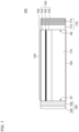
- Fig. 1 is a cross-sectional view of a semiconductor light-emitting element 100 according to a first embodiment.
- the semiconductor light-emitting element 100 is used as a light source or a gain medium of the external resonator type laser module.
- the semiconductor light-emitting element 100 includes a semiconductor substrate 110, an epitaxial layered structure 120, a P-side electrode 150, an N-side electrode 152, an AR film 160, and an HR film 170.
- the semiconductor substrate 110 is, for example, an N-type GaAs substrate.
- the epitaxial layered structure 120 is formed on the semiconductor substrate 110 by epitaxial growth.
- the epitaxial layered structure 120 includes an N-type cladding layer 122, an active layer 130, and a P-type cladding layer 124, and forms a waveguide.
- a P-type contact layer 126 made of GaAs is formed on the epitaxial layered structure 120 to enable contact with the electrode.
- a material of each layer of the epitaxial layered structure 120 is selected according to a desired wavelength, and in the present embodiment, an AIGalnP-based material is used.
- the AIGalnP-based material in the present specification is a material that can be selected from materials represented by the general formula (Al 1-x Ga x ) y In 1-y P (0 ⁇ x ⁇ 1, 0 ⁇ y ⁇ 1), and collectively represents a two element material, a three element material, and a four element material.
- layers in contact with the AR film in a wide range are the N-type cladding layer and the P-type cladding layer that occupy most of the epitaxial layered structure, and these layers have a large influence on reliability.
- the epitaxial layered structure 120 of the AIGalnP-based material mainly refers to the N-type cladding layer and the P-type cladding layer.
- the N-type cladding layer 122 is AIGalnP
- the active layer 130 is GaInP
- the P-type cladding layer 124 is AllnP.
- the active layer is selected according to a desired wavelength, and may be GaInAsP.
- the P-side electrode 150 is formed on the P-type contact layer 126, and the N-side electrode 152 is formed on a back surface of the semiconductor substrate 110.
- the AR film 160 is formed on an end surface (emission side end surface, front end surface) S1 on the emission side.
- the AR film 160 includes two layers, and includes a first layer 162 and a second layer 164.
- the first layer 162 is made of alumina (Al 2 O 3 ) as a main material on the emission side end surface S1.
- the first layer 162 is formed such that a rare gas element is mixed in amorphous Al 2 O 3 .
- the rare gas element is specifically helium (He), argon (Ar), neon (Ne), krypton (Kr), xenon (Xe), or radon (Rn), but Ar is suitable from the viewpoint of affinity with a semiconductor manufacturing process.
- the film thickness d 1 of the first layer 162 serving as a crystal protection layer is preferably from 5 nm to 120 nm.
- the film thickness d 1 is 5 nm or less, a uniform film cannot be formed, the surface cannot be sufficiently terminated, and ingress of moisture from the outside cannot be prevented.
- the film thickness d 1 is too thick, a band (wavelength range) in which the reflectance of the AR film is reduced is narrow, and it is extremely difficult to control a film thickness of a reflectance adjustment layer in a case where desired reflectance is to be obtained.
- the second layer 164 is formed on the first layer 162.
- the second layer 164 may be made of an insulator material other than Al 2 O 3 , and preferably made of an insulator material having high stability in air, such as AIN or SiN.
- the second layer 164 serving as the reflectance adjustment layer when there is a refractive index variation due to incorporation of the rare gas element, an optical film thickness represented by a product of the refractive index and the film thickness varies. Thus, even when film formation can be performed with an accurate film thickness, the optical film thickness deviates from an optimum value, so that the reflectance cannot be sufficiently reduced. Thus, it is preferable to reduce the rare gas element content of the reflectance adjustment layer as much as possible.
- the rare gas element content of the first layer 162 is configured to be larger than the rare gas element content of the second layer 164. More specifically, the rare gas element content of the first layer 162 is preferably 0.2at% or more and 5at% or less.
- the first layer 162 can be formed by a sputtering method, and in this case, a desired amount of the rare gas element can be mixed into Al 2 O 3 by adjusting the concentration of a sputtering atmosphere gas.
- an AR coated element when the reflectance increases for some reason with long-term use, a residual reflectance loss on the element front end surface increases in use in a light source for the external resonator or the like. Thus, when the reflectance increases by a certain amount or more, a failure may occur. The failure of such a mode is also caused by alteration of the crystal at the end surface portion of the semiconductor crystal due to diffusion of moisture from the outside. In the AR coated element designed to have the lowest reflectance in the initial state, the reflectance increases when the refractive index changes due to the alteration of the crystal.
- the crystal protection layer in contact with the semiconductor crystal is preferably a dense film containing a certain amount or more of Ar, and the Ar concentration in the film is desirably 0.2at% or more.
- the Ar concentration is desirably 5at% or less.
- the rare gas element content in the second layer 164 is 0.2at% or less, more preferably 0.1at% or less.
- the rare gas element content here is a concept including 0, and the second layer 164 need not contain the rare gas element.
- the first layer 162 functions as a protection layer for the epitaxial layered structure 120 which is the AIGalnP-based material.
- the second layer 164 has a function as the reflectance adjustment layer that adjusts the reflectance of the AR film 160 as a whole.
- the film thickness of the second layer 164 needs to be controlled with high accuracy so as to minimize the reflectance, and is preferably formed using a vapor deposition method.
- the film thickness is preferably controlled so as to minimize the intensity of the emitted light while monitoring the light emitted from the emission side end surface S1 in-situ in a state where power is supplied to the semiconductor light-emitting element 100 to cause the semiconductor light-emitting element 100 to emit light during film formation of the second layer 164.
- the high-reflection (HR) film 170 is formed on an end surface (rear end surface) S2 on the opposite to the emission side.
- the structure of the HR film 170 is not particularly limited, and a known technique may be used.
- a two-layer structure of a first layer 172 and a second layer 174 may be adopted.
- the first layer 172 may have a function as a protection layer.
- the second layer 174 is, for example, a dielectric multilayer film, and the number of layers and the thickness of each layer are controlled so as to obtain high reflectance at the oscillation wavelength of the laser.
- the above is the configuration of the semiconductor light-emitting element 100.
- the AR film 160 has the multilayer structure including the first layer 162 and the second layer 164.
- the AIGalnP-based material is weak against oxidation, but Al in Al 2 O 3 constituting the first layer 162 traps oxygen, so that AlGaInP can be protected from oxidation.
- Al 2 O 3 is used as a material for ceramic
- Al 2 O 3 has a property of easily permeating water, and cannot secure the long-term reliability of AIGalnP as it is.
- a dense Al 2 O 3 film can be formed, which can prevent permeation of water.
- a film formed by the sputtering method using the rare gas element has high adhesion to the crystal and is dense.
- the film thickness of the second layer 164 by controlling the film thickness of the second layer 164 with high accuracy in the order of 1 nm or less, reflectance of 0.2% or less, more preferably 0.1% or less can be achieved at a wavelength in a 600 nm band to a 700 nm band.
- the refractive index of the film itself deviates from a theoretical value.
- the end surface film can effectively reduce the reflectance by designing the optical film thickness, which is the product of the refractive index and the film thickness, to be ⁇ /4.
- the optical film thickness which is the product of the refractive index and the film thickness, changes, and deviation from a calculated value occurs.
- the variation of the refractive index needs to be suppressed and film formation of a material having a stable refractive index needs to be performed.
- the rare gas element content in the second layer 164 serving as the reflectance adjustment layer is intentionally made smaller than that in the first layer 162 serving as the crystal protection layer.
- the semiconductor light-emitting element 100 including the AR film 160 having long-term reliability and low reflectance can be provided.
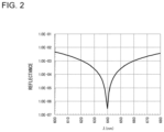
- Fig. 2 is a diagram illustrating reflectance characteristics of the AR film 160 according to the first embodiment
- a refractive index n s of the waveguide has a value between 3.0 to 3.6 depending on a composition of the AIGalnP-based material.
- the refractive index n s of the waveguide is considered as 3.3.
- the film thickness d 1 of the first layer 162 preferably satisfies d 1 ⁇ ⁇ P /(2n 1 ) where the emission peak wavelength of the semiconductor light-emitting element is ⁇ P .
- the film thickness d 1 of the first layer preferably satisfies d 1 ⁇ ⁇ P /(4n 1 )
- the film thickness d 2 of the second layer preferably satisfies d 2 ⁇ ⁇ P /(4n 2 ).
- n 1 ⁇ ⁇ n s ⁇ n 2 is established.
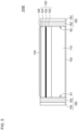
- Fig. 3 is a cross-sectional view of a semiconductor light-emitting element 100A according to a second embodiment.
- an AR film 160A has a three-layer structure, and specifically includes, in addition to the first layer 162 and the second layer 164, an intermediate layer 166 inserted therebetween.
- the first layer 162 is Al 2 O 3 as described above, and AIN can be selected as the second layer 164. Similarly to the first layer 162, Al 2 O 3 can be selected as the intermediate layer 166, but a refractive index n 3 of the intermediate layer 166 is different from the refractive index n 2 of the first layer 162.
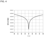
- Fig. 4 is a diagram illustrating reflectance characteristics of the AR film 160A according to the second embodiment; The calculation was performed under the following conditions.
- Fig. 5 is a cross-sectional view of a semiconductor light-emitting element 100B according to a third embodiment.
- an AR film 180 is also formed on a rear end surface S2.
- the AR film 180 is similar to the AR film 160, that is, a two-layer structure of a first layer 182 and a second layer 184 may be adopted.
- the first layer 182 may have a function as the crystal protection layer.
- the second layer 184 may have a function as the reflectance adjustment layer.
- the second layer 184 is made of, for example, an insulator material or a dielectric multilayer film, and is adjusted so as to obtain low reflectance with respect to the oscillation wavelength of the laser.
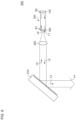
- Fig. 6 is a view illustrating an external resonator type laser module 200 including the semiconductor light-emitting element 100.
- the laser module 200 includes the semiconductor light-emitting element 100, a grating element 210, and a lens 220.
- a resonator is configured between an HR film 170 of the semiconductor light-emitting element 100 and the grating element 210.
- Light L1 emitted from the emission side end surface S1 of the semiconductor light-emitting element 100 is collimated by the lens 220, and the collimated light L2 is incident on the grating element 210.
- 0th-order diffracted light L3 of the grating element 210 is extracted to the outside as emitted light L4 of the laser module 200.
- First-order diffracted light L5 of the grating element 210 is condensed by the lens 220 and is incident on a waveguide inside the semiconductor light-emitting element 100 from the emission side end surface S1 of the semiconductor light-emitting element 100.
- Light L6 incident on the waveguide of the semiconductor light-emitting element 100 is amplified in the semiconductor light-emitting element 100 and totally reflected by the HR film 170.
- a reflection optical system such as a grating or a mirror is also disposed on the rear end surface side.
Landscapes
- Physics & Mathematics (AREA)
- Condensed Matter Physics & Semiconductors (AREA)
- General Physics & Mathematics (AREA)
- Electromagnetism (AREA)
- Optics & Photonics (AREA)
- Semiconductor Lasers (AREA)
Abstract
Description
- The present disclosure relates to a semiconductor light-emitting element used for an external resonator type semiconductor laser.
- In recent years, external resonator type semiconductor lasers have been utilized. In the external resonator type semiconductor laser, a semiconductor laser element is used as a semiconductor light amplifying element, and a laser resonator is formed between a diffraction grating provided outside the semiconductor laser element and a rear end surface of the semiconductor laser. By installing a mirror so as to reflect only a specific wavelength by the diffraction grating, oscillation occurs only in a single longitudinal mode, and narrowing of a line width of emitted light is achieved.
- As compared with a distributed feedback (DFB) laser or a distributed Bragg reflector (DBR) laser each having a diffraction grating structure in the semiconductor laser element, the mirror exists outside, and thus high output can be easily achieved. From such characteristics, the external resonator type semiconductor laser is applied to applications requiring light of a specific wavelength with high output, such as optical communication, optical measurement, and laser cooling.
- In the external resonator type semiconductor laser as described above, antireflection film (AR) coating is applied to adjust reflectance of an emission side end surface of the semiconductor laser element functioning as the semiconductor light amplifying element. As the reflectance decreases, a loss as an external resonator is reduced, and thus the reflectance is required to be as close to 0% (about 0.01 %) as possible. Specifically, the reflectance of 0.2% or less, preferably 0.1% or less is required at a desired wavelength.
- Thus, the AR film is designed so that the reflectance is the lowest at the desired wavelength, but when the film thickness varies, the wavelength at which the reflectance is the lowest point shifts, and the reflectance at the desired wavelength increases.
- Accuracy required for the film thickness of the AR film becomes more severe as an oscillation wavelength of the laser is shorter. In a case of a laser in a 600 nm band to a 700 nm band, film thickness control in the order of 1 nm or less is required to obtain a low reflection film having the reflectance of 0.1% or less, and it is very difficult to achieve the film thickness control by simply controlling a flow condition of a film formation material and film formation time. In order to solve such a problem, a method has been proposed (
JP H6-125149 A - Patent Literature 1:
JP H6-125149 A - Patent Literature 2:
US 6,297,066 - Patent Literature 3:
JP H4-299591 A - Patent Literature 4:
JP 4621791 B2 - In a laser in a 600 nm band to a 700 nm band, an AIGalnP-based material is used as a semiconductor material. The AIGalnP-based material is chemically unstable as compared with a GaAs (AlGaAs)-based material. Specifically, the AIGaInP-based material is weak against degradation due to oxidation, and thus a film that can be used for AR coating is limited. In addition, in order to ensure long-term reliability of the laser, ingress of water needs to be prevented.
- An aspect of the present disclosure has been made in view of such a problem, and one of its exemplary object is to provide a semiconductor light-emitting element including an AR film having long-term reliability and low reflectance.
- A semiconductor light-emitting element according to an aspect of the present disclosure includes a semiconductor substrate, an epitaxial layered structure formed on the semiconductor substrate, including an N-type cladding layer, an active layer, and a P-type cladding layer, and made of an AIGalnP-based material, and an anti-reflection (AR) film including a first layer containing Al2O3 formed on an emission side end surface of the epitaxial layered structure, and a second layer formed on the first layer. A rare gas element content of the first layer is larger than a rare gas element content of the second layer.
- Note that any combination of the above components and mutual replacement of the components and expressions among methods, apparatuses, systems, and the like are also effective as embodiments of the present disclosure or the present disclosure. Furthermore, the description of this item (SOLUTION TO PROBLEM) does not describe all essential features of the invention, and thus subcombinations of these features described may also be the invention.
- According to an aspect of the present disclosure, a semiconductor light-emitting element including an AR film having long-term reliability and low reflectance can be provided.
-
-
Fig. 1 is a cross-sectional view of a semiconductor light-emitting element according to a first embodiment; -
Fig. 2 is a diagram illustrating reflectance characteristics of an AR film according to the first embodiment; -
Fig. 3 is a cross-sectional view of a semiconductor light-emitting element according to a second embodiment; -
Fig. 4 is a diagram illustrating reflectance characteristics of an AR film according to the second embodiment; -
Fig. 5 is a cross-sectional view of a semiconductor light-emitting element according to a third embodiment; and -
Fig. 6 is a view illustrating an external resonator type laser module including a semiconductor light-emitting element. - An outline of some exemplary embodiments of the present disclosure will be described. This outline is intended as a prelude to the detailed description that follows, or for a basic understanding of the embodiments. This outline describes some concepts of one or more embodiments in a simplified manner, and is not intended to limit the scope of the invention or disclosure. Also, this outline is not a comprehensive outline of all possible embodiments and is not intended to limit the essential components of the embodiments. For convenience, the term "one embodiment" may be used to refer to one embodiment (an example or a variation) or a plurality of embodiments (examples or variations) disclosed in the present specification.
- A semiconductor light-emitting element according to an embodiment includes a semiconductor substrate, an epitaxial layered structure formed on the semiconductor substrate, including an N-type cladding layer, an active layer, and a P-type cladding layer, and made of an AIGalnP-based material, and an anti-reflection (AR) film including a first layer containing alumina (Al2O3) formed on an emission side end surface of the epitaxial layered structure, and a second layer formed on the first layer. A rare gas element content of the first layer is larger than a rare gas element content of the second layer.
- In this configuration, the AR film has a multilayer structure including a first layer and a second layer. AIGalnP is weak against oxidation, but Al2O3 constituting the first layer traps oxygen, so that AIGalnP can be protected from oxidation. On the other hand, as can be seen from the fact that amorphous Al2O3 is used as a material of a porous ceramic, the density of Al2O3 is reduced depending on manufacturing conditions or the like, and Al2O3 may have a property of easily permeating water. Then, long-term reliability of AIGalnP cannot be secured. By intentionally containing the rare gas element in Al2O3, a dense film can be formed, which can prevent permeation of water.
- In one embodiment, the rare gas element may be argon (Ar).
- In one embodiment, the reflectance of the emission side end surface may be 0.2% or less at the same wavelength as the peak wavelength of emitted light.
- In one embodiment, the rare gas element content in the first layer may be 0.2at% or more. Thus, a denser film can be formed. When the rare gas element content exceeds 5at%, a crystal state itself of the material constituting the film collapses to the contrary, and it becomes difficult to form the dense film. Thus, the rare gas element content in the first layer is desirably 5at% or less.
- In one embodiment, the rare gas element content in the second layer may be less than 0.2at%.
- In one embodiment, a film thickness d1 of the first layer may satisfy d1 ≤ λP/(2n1) where λP is an emission peak wavelength of the semiconductor light-emitting element, and n1 is a refractive index of the first layer.
- In one embodiment, the film thickness d1 of the first layer may satisfy d1 ≤ λP/(4n1) where λP is an emission peak wavelength of the semiconductor light-emitting element, and n1 is a refractive index of the first layer, and a film thickness d2 of the second layer may satisfy d2 ≤ λP/(4n2) where n2 is a refractive index of the second layer.
- In one embodiment, the film thickness d1 of the first layer and the film thickness d2 of the second layer may satisfy d1 > d2.
- In one embodiment, the film thickness d1 of the first layer may satisfy d1 > 5 nm.
- An external resonator type laser module according to an embodiment includes the semiconductor light-emitting element according to any one of the above and a grating element.
- Hereinafter, the present disclosure will be described based on a preferred embodiment with reference to the drawings. The same or equivalent components, members, and processing illustrated in the drawings are denoted by the same reference numerals, and redundant description will be omitted as appropriate. In addition, the exemplary embodiment is not intended to limit the disclosure, but is merely an example, and all features described in the exemplary embodiment and combinations thereof are not necessarily essential to the disclosure.
- Dimensions (thickness, length, width, and the like) of each member described in the drawings may be enlarged or reduced for easy understanding as appropriate. Furthermore, the dimensions of the plurality of members do not necessarily indicate the magnitude relationship therebetween, and even if a certain member A is drawn thicker than another member B in the drawing, the member A may be thinner than the member B.
-
Fig. 1 is a cross-sectional view of a semiconductor light-emittingelement 100 according to a first embodiment. The semiconductor light-emittingelement 100 is used as a light source or a gain medium of the external resonator type laser module. The semiconductor light-emittingelement 100 includes asemiconductor substrate 110, an epitaxiallayered structure 120, a P-side electrode 150, an N-side electrode 152, anAR film 160, and anHR film 170. - The
semiconductor substrate 110 is, for example, an N-type GaAs substrate. The epitaxiallayered structure 120 is formed on thesemiconductor substrate 110 by epitaxial growth. The epitaxiallayered structure 120 includes an N-type cladding layer 122, anactive layer 130, and a P-type cladding layer 124, and forms a waveguide. In the present embodiment, a P-type contact layer 126 made of GaAs is formed on the epitaxiallayered structure 120 to enable contact with the electrode. A material of each layer of the epitaxiallayered structure 120 is selected according to a desired wavelength, and in the present embodiment, an AIGalnP-based material is used. Note that the AIGalnP-based material in the present specification is a material that can be selected from materials represented by the general formula (Al1-xGax)yIn1-yP (0 ≤ x ≤ 1, 0 ≤ y ≤ 1), and collectively represents a two element material, a three element material, and a four element material. In the epitaxiallayered structure 120, layers in contact with the AR film in a wide range are the N-type cladding layer and the P-type cladding layer that occupy most of the epitaxial layered structure, and these layers have a large influence on reliability. Thus, the epitaxiallayered structure 120 of the AIGalnP-based material mainly refers to the N-type cladding layer and the P-type cladding layer. For example, the N-type cladding layer 122 is AIGalnP, theactive layer 130 is GaInP, and the P-type cladding layer 124 is AllnP. The active layer is selected according to a desired wavelength, and may be GaInAsP. - The P-
side electrode 150 is formed on the P-type contact layer 126, and the N-side electrode 152 is formed on a back surface of thesemiconductor substrate 110. - When the semiconductor light-emitting
element 100 is incorporated in the external resonator type laser module, theAR film 160 is formed on an end surface (emission side end surface, front end surface) S1 on the emission side. - The
AR film 160 includes two layers, and includes afirst layer 162 and asecond layer 164. Thefirst layer 162 is made of alumina (Al2O3) as a main material on the emission side end surface S1. Thefirst layer 162 is formed such that a rare gas element is mixed in amorphous Al2O3. The rare gas element is specifically helium (He), argon (Ar), neon (Ne), krypton (Kr), xenon (Xe), or radon (Rn), but Ar is suitable from the viewpoint of affinity with a semiconductor manufacturing process. - The film thickness d1 of the
first layer 162 serving as a crystal protection layer is preferably from 5 nm to 120 nm. When the film thickness d1 is 5 nm or less, a uniform film cannot be formed, the surface cannot be sufficiently terminated, and ingress of moisture from the outside cannot be prevented. When the film thickness d1 is too thick, a band (wavelength range) in which the reflectance of the AR film is reduced is narrow, and it is extremely difficult to control a film thickness of a reflectance adjustment layer in a case where desired reflectance is to be obtained. - The
second layer 164 is formed on thefirst layer 162. Thesecond layer 164 may be made of an insulator material other than Al2O3, and preferably made of an insulator material having high stability in air, such as AIN or SiN. - With respect to the
second layer 164 serving as the reflectance adjustment layer, when there is a refractive index variation due to incorporation of the rare gas element, an optical film thickness represented by a product of the refractive index and the film thickness varies. Thus, even when film formation can be performed with an accurate film thickness, the optical film thickness deviates from an optimum value, so that the reflectance cannot be sufficiently reduced. Thus, it is preferable to reduce the rare gas element content of the reflectance adjustment layer as much as possible. - That is, in the present embodiment, the rare gas element content of the
first layer 162 is configured to be larger than the rare gas element content of thesecond layer 164. More specifically, the rare gas element content of thefirst layer 162 is preferably 0.2at% or more and 5at% or less. - For example, the
first layer 162 can be formed by a sputtering method, and in this case, a desired amount of the rare gas element can be mixed into Al2O3 by adjusting the concentration of a sputtering atmosphere gas. - There is also a report that, in a normal semiconductor laser element, when the rare gas element content increases, heat is generated by light absorption by the rare gas element, and the element is deteriorated by COD (
JP 4621791 B2 - In the present embodiment, by coating the outermost surface of the semiconductor crystal with the dense crystal protection layer, moisture that permeates to the crystal end surface through the end surface film during operation can be suppressed, so that such a failure mode can be suppressed. Thus, the crystal protection layer in contact with the semiconductor crystal is preferably a dense film containing a certain amount or more of Ar, and the Ar concentration in the film is desirably 0.2at% or more. On the other hand, when the Ar concentration is too high, the crystalline state itself of the material for forming the crystal protection layer collapses, and a dense film cannot be formed to the contrary. Thus, the Ar concentration is desirably 5at% or less.
- On the other hand, the rare gas element content in the
second layer 164 is 0.2at% or less, more preferably 0.1at% or less. The rare gas element content here is a concept including 0, and thesecond layer 164 need not contain the rare gas element. - The
first layer 162 functions as a protection layer for the epitaxiallayered structure 120 which is the AIGalnP-based material. On the other hand, thesecond layer 164 has a function as the reflectance adjustment layer that adjusts the reflectance of theAR film 160 as a whole. Thus, the film thickness of thesecond layer 164 needs to be controlled with high accuracy so as to minimize the reflectance, and is preferably formed using a vapor deposition method. More preferably, the film thickness is preferably controlled so as to minimize the intensity of the emitted light while monitoring the light emitted from the emission side end surface S1 in-situ in a state where power is supplied to the semiconductor light-emittingelement 100 to cause the semiconductor light-emittingelement 100 to emit light during film formation of thesecond layer 164. - When the semiconductor light-emitting
element 100 is incorporated in the external resonator type laser module, the high-reflection (HR)film 170 is formed on an end surface (rear end surface) S2 on the opposite to the emission side. The structure of theHR film 170 is not particularly limited, and a known technique may be used. A two-layer structure of afirst layer 172 and asecond layer 174 may be adopted. Thefirst layer 172 may have a function as a protection layer. Thesecond layer 174 is, for example, a dielectric multilayer film, and the number of layers and the thickness of each layer are controlled so as to obtain high reflectance at the oscillation wavelength of the laser. - The above is the configuration of the semiconductor light-emitting
element 100. - In the present embodiment, the
AR film 160 has the multilayer structure including thefirst layer 162 and thesecond layer 164. The AIGalnP-based material is weak against oxidation, but Al in Al2O3 constituting thefirst layer 162 traps oxygen, so that AlGaInP can be protected from oxidation. - On the other hand, as can be seen from the fact that Al2O3 is used as a material for ceramic, Al2O3 has a property of easily permeating water, and cannot secure the long-term reliability of AIGalnP as it is. In the present embodiment, by intentionally containing the rare gas element in Al2O3, a dense Al2O3 film can be formed, which can prevent permeation of water. In particular, a film formed by the sputtering method using the rare gas element has high adhesion to the crystal and is dense. As a result, defects present on the surface of the semiconductor crystal are terminated, and deterioration originating from the defects is suppressed, and in addition, permeation of moisture from the outside is suppressed, and thus the alteration of the crystal can be suppressed, and deterioration of long-term reliability can be suppressed.
- Then, by controlling the film thickness of the
second layer 164 with high accuracy in the order of 1 nm or less, reflectance of 0.2% or less, more preferably 0.1% or less can be achieved at a wavelength in a 600 nm band to a 700 nm band. When thesecond layer 164 contains the rare gas element, the refractive index of the film itself deviates from a theoretical value. The end surface film can effectively reduce the reflectance by designing the optical film thickness, which is the product of the refractive index and the film thickness, to be λ/4. However, when the refractive index of thesecond layer 164 varies due to mixing of the rare gas element, the optical film thickness, which is the product of the refractive index and the film thickness, changes, and deviation from a calculated value occurs. Thus, in order to improve controllability of the reflectance, the variation of the refractive index needs to be suppressed and film formation of a material having a stable refractive index needs to be performed. In the present embodiment, the rare gas element content in thesecond layer 164 serving as the reflectance adjustment layer is intentionally made smaller than that in thefirst layer 162 serving as the crystal protection layer. As a result, by suppressing the refractive index variation caused by the rare gas element and by performing film formation with a predetermined film thickness, desired reflectance can be stably obtained, and good AR coating characteristics can be obtained. - As described above, according to the present embodiment, the semiconductor light-emitting
element 100 including theAR film 160 having long-term reliability and low reflectance can be provided. -
Fig. 2 is a diagram illustrating reflectance characteristics of theAR film 160 according to the first embodiment; In the AIGalnP-based material, a refractive index ns of the waveguide has a value between 3.0 to 3.6 depending on a composition of the AIGalnP-based material. Now, the refractive index ns of the waveguide is considered as 3.3. Thefirst layer 162 serving as the crystal protection layer is made of Al2O3 having a refractive index n1 = 1.75, and thesecond layer 164 serving as the reflectance adjustment layer is made of AlN having a refractive index n2 = 2.17. - The film thickness d1 of the
first layer 162 preferably satisfies d1 ≤ λP/(2n1) where the emission peak wavelength of the semiconductor light-emitting element is λP. - Furthermore, in a case where the
AR film 160 has a two-layer structure of thefirst layer 162 and thesecond layer 164, the film thickness d1 of the first layer preferably satisfies d1 ≤ λP/(4n1), and the film thickness d2 of the second layer preferably satisfies d2 ≤ λP/(4n2). - The film thickness of the
first layer 162 is d1 = 62.2 nm, and the film thickness of thesecond layer 164 is d2 = 17.2 nm. In the relationship between the refractive indexes at this time,
- According to this AR film, reflectance of 10-6 or less is obtained at a wavelength of 640 nm.
-
Fig. 3 is a cross-sectional view of a semiconductor light-emittingelement 100A according to a second embodiment. In the semiconductor light-emittingelement 100A, anAR film 160A has a three-layer structure, and specifically includes, in addition to thefirst layer 162 and thesecond layer 164, anintermediate layer 166 inserted therebetween. - The
first layer 162 is Al2O3 as described above, and AIN can be selected as thesecond layer 164. Similarly to thefirst layer 162, Al2O3 can be selected as theintermediate layer 166, but a refractive index n3 of theintermediate layer 166 is different from the refractive index n2 of thefirst layer 162. -
Fig. 4 is a diagram illustrating reflectance characteristics of theAR film 160A according to the second embodiment; The calculation was performed under the following conditions. - Refractive index ns of waveguide = 3.3
- First layer 162: material Al2O3, refractive index n1 = 1.75, film thickness d1 = 39.3 nm
- Intermediate layer 166: material Al2O3, refractive index n3 = 1.70, film thickness d3 = 20.2 nm Second layer 164: material AIN, refractive index n2 = 2.17, film thickness d2 = 19.5 nm Also in this case, similarly, reflectance of 10-6 or less is obtained at 640 nm.
-
Fig. 5 is a cross-sectional view of a semiconductor light-emittingelement 100B according to a third embodiment. In the semiconductor light-emittingelement 100B, anAR film 180 is also formed on a rear end surface S2. TheAR film 180 is similar to theAR film 160, that is, a two-layer structure of afirst layer 182 and asecond layer 184 may be adopted. Thefirst layer 182 may have a function as the crystal protection layer. Thesecond layer 184 may have a function as the reflectance adjustment layer. Thesecond layer 184 is made of, for example, an insulator material or a dielectric multilayer film, and is adjusted so as to obtain low reflectance with respect to the oscillation wavelength of the laser. - The semiconductor light-emitting
elements Fig. 6 is a view illustrating an external resonatortype laser module 200 including the semiconductor light-emittingelement 100. - The
laser module 200 includes the semiconductor light-emittingelement 100, agrating element 210, and alens 220. In thelaser module 200, a resonator is configured between anHR film 170 of the semiconductor light-emittingelement 100 and thegrating element 210. Light L1 emitted from the emission side end surface S1 of the semiconductor light-emittingelement 100 is collimated by thelens 220, and the collimated light L2 is incident on thegrating element 210. 0th-order diffracted light L3 of thegrating element 210 is extracted to the outside as emitted light L4 of thelaser module 200. First-order diffracted light L5 of thegrating element 210 is condensed by thelens 220 and is incident on a waveguide inside the semiconductor light-emittingelement 100 from the emission side end surface S1 of the semiconductor light-emittingelement 100. Light L6 incident on the waveguide of the semiconductor light-emittingelement 100 is amplified in the semiconductor light-emittingelement 100 and totally reflected by theHR film 170. - In the
laser module 200 including the semiconductor light-emittingelement 100B described in the third embodiment, a reflection optical system such as a grating or a mirror is also disposed on the rear end surface side. - The embodiments merely illustrate the principle and applications of the present invention, and many modifications and changes in arrangement can be made in the embodiments without departing from the spirit of the present invention defined in the claims.
-
- 100
- Semiconductor light-emitting element
- 110
- Semiconductor substrate
- 120
- epitaxial layered structure
- 122
- N-type cladding layer
- 124
- P-type cladding layer
- 126
- P-type contact layer
- 130
- Active layer
- 150
- P-side electrode
- 152
- N-side electrode
- 160
- AR film
- 162
- First layer
- 164
- Second layer
- 166
- Intermediate layer
- 170
- HR film
- 172
- First layer
- 174
- Second layer
- 180
- AR film
- 182
- First layer
- 184
- Second layer
- 200
- Laser module
- 210
- Grating element
- 220
- Lens
Claims (9)
- A semiconductor light-emitting element (100) comprising:a semiconductor substrate (110);an epitaxial layered structure (120) formed on the semiconductor substrate (110), including an N-type cladding layer (122), an active layer (130), and a P-type cladding layer (124), and made of an AIGalnP-based material; andan anti-reflection (AR) film (160) including a first layer (162) containing Al2O3 formed on an emission side end surface (S1) of the epitaxial layered structure (120), and a second layer (164) formed on the first layer (162), whereina rare gas element content of the first layer (162) is larger than a rare gas element content of the second layer (164).
- The semiconductor light-emitting element (100) according to claim 1, wherein reflectance of the emission side end surface (S1) is 0.2% or less at the same wavelength as a peak wavelength of emitted light.
- The semiconductor light-emitting element (100) according to claim 1 or 2, wherein the rare gas element content in the first layer (162) is 0.2at% or more and 5at% or less.
- The semiconductor light-emitting element (100) according to claim 1 or 2, wherein the rare gas element content in the second layer (164) is less than 0.2at%.
- The semiconductor light-emitting element (100) according to claim 2, wherein a film thickness d1 of the first layer (162) satisfies d1 ≤ λP/(2n1), where λP is an emission peak wavelength of the semiconductor light-emitting element (100), and n1 is a refractive index of the first layer (162).
- The semiconductor light-emitting element (100) according to claim 1, whereina film thickness d1 of the first layer (162) satisfies d1 ≤ λP/(4n1), where λP is an emission peak wavelength of the semiconductor light-emitting element (100), and n1 is a refractive index of the first layer (162), anda film thickness d2 of the second layer (164) satisfies d2 ≤ λP/(4n2), where n2 is a refractive index of the second layer (164).
- The semiconductor light-emitting element (100) according to claim 6, wherein the film thickness d1 of the first layer (162) and the film thickness d2 of the second layer (164) satisfy d1 > d2.
- The semiconductor light-emitting element (100) according to claim 1 or 2, wherein a film thickness d1 of the first layer (162) satisfies d1 > 5 nm.
- An external resonator type laser module (200) comprising:the semiconductor light-emitting element (100) according to any one of claims 1 to 8; anda grating element (210).
Applications Claiming Priority (1)
| Application Number | Priority Date | Filing Date | Title |
|---|---|---|---|
| JP2023113226A JP2025010917A (en) | 2023-07-10 | 2023-07-10 | Semiconductor light emitting element and external cavity laser module |
Publications (2)
| Publication Number | Publication Date |
|---|---|
| EP4492592A1 true EP4492592A1 (en) | 2025-01-15 |
| EP4492592B1 EP4492592B1 (en) | 2026-01-28 |
Family
ID=91782331
Family Applications (1)
| Application Number | Title | Priority Date | Filing Date |
|---|---|---|---|
| EP24186042.8A Active EP4492592B1 (en) | 2023-07-10 | 2024-07-02 | Semiconductor light-emitting element and external resonator type laser module |
Country Status (2)
| Country | Link |
|---|---|
| EP (1) | EP4492592B1 (en) |
| JP (1) | JP2025010917A (en) |
Citations (6)
| Publication number | Priority date | Publication date | Assignee | Title |
|---|---|---|---|---|
| JPH04299591A (en) | 1991-03-27 | 1992-10-22 | Canon Inc | Semiconductor element and its manufacture |
| JPH06125149A (en) | 1992-10-12 | 1994-05-06 | Canon Inc | Semiconductor device and manufacturing method thereof |
| US6297066B1 (en) | 1998-03-21 | 2001-10-02 | Joachim Sacher | Coating process and apparatus |
| US20050127383A1 (en) * | 2003-12-10 | 2005-06-16 | Takeshi Kikawa | Laser diode and manufacturing method thereof |
| US20090086782A1 (en) * | 2007-09-28 | 2009-04-02 | Matsushita Electric Industrial Co., Ltd. | Semiconductor laser device and method for manufacturing the same |
| US20100316082A1 (en) * | 2009-06-11 | 2010-12-16 | Yoshinobu Kawaguchi | Nitride semiconductor laser chip |
-
2023
- 2023-07-10 JP JP2023113226A patent/JP2025010917A/en active Pending
-
2024
- 2024-07-02 EP EP24186042.8A patent/EP4492592B1/en active Active
Patent Citations (7)
| Publication number | Priority date | Publication date | Assignee | Title |
|---|---|---|---|---|
| JPH04299591A (en) | 1991-03-27 | 1992-10-22 | Canon Inc | Semiconductor element and its manufacture |
| JPH06125149A (en) | 1992-10-12 | 1994-05-06 | Canon Inc | Semiconductor device and manufacturing method thereof |
| US6297066B1 (en) | 1998-03-21 | 2001-10-02 | Joachim Sacher | Coating process and apparatus |
| US20050127383A1 (en) * | 2003-12-10 | 2005-06-16 | Takeshi Kikawa | Laser diode and manufacturing method thereof |
| US20090086782A1 (en) * | 2007-09-28 | 2009-04-02 | Matsushita Electric Industrial Co., Ltd. | Semiconductor laser device and method for manufacturing the same |
| US20100316082A1 (en) * | 2009-06-11 | 2010-12-16 | Yoshinobu Kawaguchi | Nitride semiconductor laser chip |
| JP4621791B2 (en) | 2009-06-11 | 2011-01-26 | シャープ株式会社 | Nitride semiconductor laser device |
Also Published As
| Publication number | Publication date |
|---|---|
| JP2025010917A (en) | 2025-01-23 |
| EP4492592B1 (en) | 2026-01-28 |
Similar Documents
| Publication | Publication Date | Title |
|---|---|---|
| Fiebig et al. | 12 W high-brightness single-frequency DBR tapered diode laser | |
| JP2971435B2 (en) | Semiconductor laser and method of manufacturing the same | |
| CN102570298B (en) | Laser diode module and semi-conductor optical amplifier assembly | |
| JP3729170B2 (en) | Semiconductor laser | |
| US5260822A (en) | Tapered semiconductor laser gain structure with cavity spoiling grooves | |
| KR101760937B1 (en) | Vertical cavity surface emitting laser | |
| JP5631692B2 (en) | Semiconductor laser device assembly | |
| JP2005175111A (en) | Semiconductor laser and manufacturing method thereof | |
| US6898224B2 (en) | Semiconductor laser device | |
| CA2371504C (en) | Semiconductor laser device and optical fiber amplifier | |
| JP2002223028A (en) | Semiconductor light emitting device | |
| WO2000046893A1 (en) | Semiconductor laser and semiconductor laser module using the same | |
| US7627010B2 (en) | Semiconductor laser having Fabry-Perot resonator | |
| EP4492592B1 (en) | Semiconductor light-emitting element and external resonator type laser module | |
| JP2005209952A (en) | Semiconductor laser device and optical pickup device using the same | |
| JP2011086714A (en) | Wavelength tunable laser | |
| JP6934129B2 (en) | How to drive a semiconductor light emitting device assembly | |
| US7215694B2 (en) | Semiconductor laser device | |
| WO2001039340A2 (en) | Mode-selective facet layer for pump laser | |
| US20150138562A1 (en) | Wavelength-variable laser including soa and optical coherence tomography apparatus including the laser | |
| JP4599432B2 (en) | Semiconductor laser and manufacturing method thereof | |
| JP2000036633A (en) | Semiconductor laser | |
| JP3119301B2 (en) | High power semiconductor laser | |
| US6738405B1 (en) | Semiconductor laser | |
| JP4163343B2 (en) | Light emitting device and light emitting device module |
Legal Events
| Date | Code | Title | Description |
|---|---|---|---|
| PUAI | Public reference made under article 153(3) epc to a published international application that has entered the european phase |
Free format text: ORIGINAL CODE: 0009012 |
|
| STAA | Information on the status of an ep patent application or granted ep patent |
Free format text: STATUS: THE APPLICATION HAS BEEN PUBLISHED |
|
| AK | Designated contracting states |
Kind code of ref document: A1 Designated state(s): AL AT BE BG CH CY CZ DE DK EE ES FI FR GB GR HR HU IE IS IT LI LT LU LV MC ME MK MT NL NO PL PT RO RS SE SI SK SM TR |
|
| STAA | Information on the status of an ep patent application or granted ep patent |
Free format text: STATUS: REQUEST FOR EXAMINATION WAS MADE |
|
| 17P | Request for examination filed |
Effective date: 20250617 |
|
| GRAP | Despatch of communication of intention to grant a patent |
Free format text: ORIGINAL CODE: EPIDOSNIGR1 |
|
| STAA | Information on the status of an ep patent application or granted ep patent |
Free format text: STATUS: GRANT OF PATENT IS INTENDED |
|
| INTG | Intention to grant announced |
Effective date: 20250918 |
|
| RIN1 | Information on inventor provided before grant (corrected) |
Inventor name: WATANABE, KYOHEI Inventor name: HAGIMOTO, MASATO |
|
| GRAS | Grant fee paid |
Free format text: ORIGINAL CODE: EPIDOSNIGR3 |
|
| GRAA | (expected) grant |
Free format text: ORIGINAL CODE: 0009210 |
|
| STAA | Information on the status of an ep patent application or granted ep patent |
Free format text: STATUS: THE PATENT HAS BEEN GRANTED |
|
| AK | Designated contracting states |
Kind code of ref document: B1 Designated state(s): AL AT BE BG CH CY CZ DE DK EE ES FI FR GB GR HR HU IE IS IT LI LT LU LV MC ME MK MT NL NO PL PT RO RS SE SI SK SM TR |
|
| REG | Reference to a national code |
Ref country code: CH Ref legal event code: F10 Free format text: ST27 STATUS EVENT CODE: U-0-0-F10-F00 (AS PROVIDED BY THE NATIONAL OFFICE) Effective date: 20260128 Ref country code: GB Ref legal event code: FG4D |
|
| REG | Reference to a national code |
Ref country code: DE Ref legal event code: R096 Ref document number: 602024002274 Country of ref document: DE |
|
| REG | Reference to a national code |
Ref country code: IE Ref legal event code: FG4D |
|
| REG | Reference to a national code |
Ref country code: CH Ref legal event code: W10 Free format text: ST27 STATUS EVENT CODE: U-0-0-W10-W00 (AS PROVIDED BY THE NATIONAL OFFICE) Effective date: 20260325 |
|
| RAP4 | Party data changed (patent owner data changed or rights of a patent transferred) |
Owner name: USHIO DENKI KABUSHIKI KAISHA |
|
| REG | Reference to a national code |
Ref country code: NL Ref legal event code: MP Effective date: 20260128 |
|
| PG25 | Lapsed in a contracting state [announced via postgrant information from national office to epo] |
Ref country code: NL Free format text: LAPSE BECAUSE OF FAILURE TO SUBMIT A TRANSLATION OF THE DESCRIPTION OR TO PAY THE FEE WITHIN THE PRESCRIBED TIME-LIMIT Effective date: 20260128 |
|
| REG | Reference to a national code |
Ref country code: AT Ref legal event code: MK05 Ref document number: 1882824 Country of ref document: AT Kind code of ref document: T Effective date: 20260128 |
|
| PG25 | Lapsed in a contracting state [announced via postgrant information from national office to epo] |
Ref country code: RS Free format text: LAPSE BECAUSE OF FAILURE TO SUBMIT A TRANSLATION OF THE DESCRIPTION OR TO PAY THE FEE WITHIN THE PRESCRIBED TIME-LIMIT Effective date: 20260428 |
|
| PG25 | Lapsed in a contracting state [announced via postgrant information from national office to epo] |
Ref country code: PL Free format text: LAPSE BECAUSE OF FAILURE TO SUBMIT A TRANSLATION OF THE DESCRIPTION OR TO PAY THE FEE WITHIN THE PRESCRIBED TIME-LIMIT Effective date: 20260128 |
|
| PG25 | Lapsed in a contracting state [announced via postgrant information from national office to epo] |
Ref country code: GR Free format text: LAPSE BECAUSE OF FAILURE TO SUBMIT A TRANSLATION OF THE DESCRIPTION OR TO PAY THE FEE WITHIN THE PRESCRIBED TIME-LIMIT Effective date: 20260429 |
|
| REG | Reference to a national code |
Ref country code: LT Ref legal event code: MG9D |
|
| PG25 | Lapsed in a contracting state [announced via postgrant information from national office to epo] |
Ref country code: LT Free format text: LAPSE BECAUSE OF FAILURE TO SUBMIT A TRANSLATION OF THE DESCRIPTION OR TO PAY THE FEE WITHIN THE PRESCRIBED TIME-LIMIT Effective date: 20260128 |
|
| PG25 | Lapsed in a contracting state [announced via postgrant information from national office to epo] |
Ref country code: NO Free format text: LAPSE BECAUSE OF FAILURE TO SUBMIT A TRANSLATION OF THE DESCRIPTION OR TO PAY THE FEE WITHIN THE PRESCRIBED TIME-LIMIT Effective date: 20260428 |
|
| PG25 | Lapsed in a contracting state [announced via postgrant information from national office to epo] |
Ref country code: FI Free format text: LAPSE BECAUSE OF FAILURE TO SUBMIT A TRANSLATION OF THE DESCRIPTION OR TO PAY THE FEE WITHIN THE PRESCRIBED TIME-LIMIT Effective date: 20260128 Ref country code: SE Free format text: LAPSE BECAUSE OF FAILURE TO SUBMIT A TRANSLATION OF THE DESCRIPTION OR TO PAY THE FEE WITHIN THE PRESCRIBED TIME-LIMIT Effective date: 20260128 Ref country code: AT Free format text: LAPSE BECAUSE OF FAILURE TO SUBMIT A TRANSLATION OF THE DESCRIPTION OR TO PAY THE FEE WITHIN THE PRESCRIBED TIME-LIMIT Effective date: 20260128 |
|
| PG25 | Lapsed in a contracting state [announced via postgrant information from national office to epo] |
Ref country code: HR Free format text: LAPSE BECAUSE OF FAILURE TO SUBMIT A TRANSLATION OF THE DESCRIPTION OR TO PAY THE FEE WITHIN THE PRESCRIBED TIME-LIMIT Effective date: 20260128 |
|
| PG25 | Lapsed in a contracting state [announced via postgrant information from national office to epo] |
Ref country code: PT Free format text: LAPSE BECAUSE OF FAILURE TO SUBMIT A TRANSLATION OF THE DESCRIPTION OR TO PAY THE FEE WITHIN THE PRESCRIBED TIME-LIMIT Effective date: 20260528 Ref country code: IS Free format text: LAPSE BECAUSE OF FAILURE TO SUBMIT A TRANSLATION OF THE DESCRIPTION OR TO PAY THE FEE WITHIN THE PRESCRIBED TIME-LIMIT Effective date: 20260528 |
|
| PG25 | Lapsed in a contracting state [announced via postgrant information from national office to epo] |
Ref country code: LV Free format text: LAPSE BECAUSE OF FAILURE TO SUBMIT A TRANSLATION OF THE DESCRIPTION OR TO PAY THE FEE WITHIN THE PRESCRIBED TIME-LIMIT Effective date: 20260128 |
|
| PG25 | Lapsed in a contracting state [announced via postgrant information from national office to epo] |
Ref country code: BG Free format text: LAPSE BECAUSE OF FAILURE TO SUBMIT A TRANSLATION OF THE DESCRIPTION OR TO PAY THE FEE WITHIN THE PRESCRIBED TIME-LIMIT Effective date: 20260128 |