EP4492148A1 - Image carrier unit and image forming apparatus - Google Patents
Image carrier unit and image forming apparatus Download PDFInfo
- Publication number
- EP4492148A1 EP4492148A1 EP24156183.6A EP24156183A EP4492148A1 EP 4492148 A1 EP4492148 A1 EP 4492148A1 EP 24156183 A EP24156183 A EP 24156183A EP 4492148 A1 EP4492148 A1 EP 4492148A1
- Authority
- EP
- European Patent Office
- Prior art keywords
- image carrier
- image
- housing
- contact point
- unit
- Prior art date
- Legal status (The legal status is an assumption and is not a legal conclusion. Google has not performed a legal analysis and makes no representation as to the accuracy of the status listed.)
- Pending
Links
- 238000012546 transfer Methods 0.000 description 11
- 230000032258 transport Effects 0.000 description 6
- 230000007423 decrease Effects 0.000 description 3
- 238000000034 method Methods 0.000 description 3
- 230000002093 peripheral effect Effects 0.000 description 3
- 238000004140 cleaning Methods 0.000 description 2
- 238000005520 cutting process Methods 0.000 description 2
- 238000010586 diagram Methods 0.000 description 2
- 238000004519 manufacturing process Methods 0.000 description 2
- 238000012986 modification Methods 0.000 description 2
- 230000004048 modification Effects 0.000 description 2
- 239000011347 resin Substances 0.000 description 2
- 229920005989 resin Polymers 0.000 description 2
- 238000012360 testing method Methods 0.000 description 2
- 230000001464 adherent effect Effects 0.000 description 1
- 239000003086 colorant Substances 0.000 description 1
- 238000001514 detection method Methods 0.000 description 1
- 238000003780 insertion Methods 0.000 description 1
- 230000037431 insertion Effects 0.000 description 1
Images




Classifications
-
- G—PHYSICS
- G03—PHOTOGRAPHY; CINEMATOGRAPHY; ANALOGOUS TECHNIQUES USING WAVES OTHER THAN OPTICAL WAVES; ELECTROGRAPHY; HOLOGRAPHY
- G03G—ELECTROGRAPHY; ELECTROPHOTOGRAPHY; MAGNETOGRAPHY
- G03G15/00—Apparatus for electrographic processes using a charge pattern
- G03G15/02—Apparatus for electrographic processes using a charge pattern for laying down a uniform charge, e.g. for sensitising; Corona discharge devices
- G03G15/0208—Apparatus for electrographic processes using a charge pattern for laying down a uniform charge, e.g. for sensitising; Corona discharge devices by contact, friction or induction, e.g. liquid charging apparatus
- G03G15/0216—Apparatus for electrographic processes using a charge pattern for laying down a uniform charge, e.g. for sensitising; Corona discharge devices by contact, friction or induction, e.g. liquid charging apparatus by bringing a charging member into contact with the member to be charged, e.g. roller, brush chargers
- G03G15/0233—Structure, details of the charging member, e.g. chemical composition, surface properties
-
- G—PHYSICS
- G03—PHOTOGRAPHY; CINEMATOGRAPHY; ANALOGOUS TECHNIQUES USING WAVES OTHER THAN OPTICAL WAVES; ELECTROGRAPHY; HOLOGRAPHY
- G03G—ELECTROGRAPHY; ELECTROPHOTOGRAPHY; MAGNETOGRAPHY
- G03G21/00—Arrangements not provided for by groups G03G13/00 - G03G19/00, e.g. cleaning, elimination of residual charge
- G03G21/16—Mechanical means for facilitating the maintenance of the apparatus, e.g. modular arrangements
- G03G21/1642—Mechanical means for facilitating the maintenance of the apparatus, e.g. modular arrangements for connecting the different parts of the apparatus
- G03G21/1652—Electrical connection means
-
- G—PHYSICS
- G03—PHOTOGRAPHY; CINEMATOGRAPHY; ANALOGOUS TECHNIQUES USING WAVES OTHER THAN OPTICAL WAVES; ELECTROGRAPHY; HOLOGRAPHY
- G03G—ELECTROGRAPHY; ELECTROPHOTOGRAPHY; MAGNETOGRAPHY
- G03G15/00—Apparatus for electrographic processes using a charge pattern
- G03G15/75—Details relating to xerographic drum, band or plate, e.g. replacing, testing
-
- G—PHYSICS
- G03—PHOTOGRAPHY; CINEMATOGRAPHY; ANALOGOUS TECHNIQUES USING WAVES OTHER THAN OPTICAL WAVES; ELECTROGRAPHY; HOLOGRAPHY
- G03G—ELECTROGRAPHY; ELECTROPHOTOGRAPHY; MAGNETOGRAPHY
- G03G15/00—Apparatus for electrographic processes using a charge pattern
- G03G15/80—Details relating to power supplies, circuits boards, electrical connections
-
- G—PHYSICS
- G03—PHOTOGRAPHY; CINEMATOGRAPHY; ANALOGOUS TECHNIQUES USING WAVES OTHER THAN OPTICAL WAVES; ELECTROGRAPHY; HOLOGRAPHY
- G03G—ELECTROGRAPHY; ELECTROPHOTOGRAPHY; MAGNETOGRAPHY
- G03G21/00—Arrangements not provided for by groups G03G13/00 - G03G19/00, e.g. cleaning, elimination of residual charge
- G03G21/16—Mechanical means for facilitating the maintenance of the apparatus, e.g. modular arrangements
- G03G21/1642—Mechanical means for facilitating the maintenance of the apparatus, e.g. modular arrangements for connecting the different parts of the apparatus
- G03G21/1647—Mechanical connection means
-
- G—PHYSICS
- G03—PHOTOGRAPHY; CINEMATOGRAPHY; ANALOGOUS TECHNIQUES USING WAVES OTHER THAN OPTICAL WAVES; ELECTROGRAPHY; HOLOGRAPHY
- G03G—ELECTROGRAPHY; ELECTROPHOTOGRAPHY; MAGNETOGRAPHY
- G03G21/00—Arrangements not provided for by groups G03G13/00 - G03G19/00, e.g. cleaning, elimination of residual charge
- G03G21/16—Mechanical means for facilitating the maintenance of the apparatus, e.g. modular arrangements
- G03G21/1661—Mechanical means for facilitating the maintenance of the apparatus, e.g. modular arrangements means for handling parts of the apparatus in the apparatus
- G03G21/1671—Mechanical means for facilitating the maintenance of the apparatus, e.g. modular arrangements means for handling parts of the apparatus in the apparatus for the photosensitive element
-
- G—PHYSICS
- G03—PHOTOGRAPHY; CINEMATOGRAPHY; ANALOGOUS TECHNIQUES USING WAVES OTHER THAN OPTICAL WAVES; ELECTROGRAPHY; HOLOGRAPHY
- G03G—ELECTROGRAPHY; ELECTROPHOTOGRAPHY; MAGNETOGRAPHY
- G03G2221/00—Processes not provided for by group G03G2215/00, e.g. cleaning or residual charge elimination
- G03G2221/16—Mechanical means for facilitating the maintenance of the apparatus, e.g. modular arrangements and complete machine concepts
- G03G2221/1606—Mechanical means for facilitating the maintenance of the apparatus, e.g. modular arrangements and complete machine concepts for the photosensitive element
Definitions
- the present disclosure relates to an image carrier unit and an image forming apparatus.
- Japanese Unexamined Patent Application Publication No. 2008-57616 discloses a structure of a rotation shaft support device including substantially hollow cylindrical bearing members that rotatably support a rotation shaft, and holding members to which the bearing members are fixed.
- the bearing member has a bearing cutaway portion formed by cutting away part of the bearing member.
- the rotation shaft is attached into the bearing member through the bearing cutaway portion.
- the holding member has bearing fitting members formed by cutting away part of the holding member. The bearing member having the rotation shaft attached thereto is held in the bearing fitting members.
- an image carrier unit in which an image carrier that carries an image on its surface is housed in a housing member so that the image carrier is rotatable by a support member, it is necessary to check whether a conduction member for establishing electrical conduction of the image carrier is in contact with the image carrier. If the electrical conduction is not confirmed by a conduction test after assembling, the image carrier unit is disassembled to identify the cause, and whether there is a contact point where the conduction member is in contact with the image carrier is checked. Therefore, the workability decreases. If the contact point is checkable during assembling, it is less likely that the electrical conduction is not confirmed by the conduction test. Therefore, the decrease in workability during the manufacturing process may be suppressed.
- an image carrier unit comprising: an image carrier configured to carry an image on a surface of the image carrier; a conduction member configured to establish electrical conduction of the image carrier by a contact point with the image carrier; and a shape portion configured to allow viewing of the contact point.
- the shape portion is oriented in the same direction as a housing direction in which the image carrier is housed in a housing member that houses the image carrier.
- a positioning member that positions, relative to the housing member, a support member that supports the image carrier is cut away at a predetermined position relative to the housing direction.
- the shape portion is cut away up to a position of the contact point in a direction of a rotation shaft of the image carrier.
- the conduction member is configured to, when the image carrier unit is pulled from an image forming apparatus to which the image carrier unit is attached, cut off the electrical conduction of the image carrier before the shape portion is exposed from the image forming apparatus.
- an image forming apparatus comprising: an image former configured to form an image; and an image carrier unit that constitutes the image former and is insertable into and removable from an apparatus body including the image former.
- the image carrier unit comprises: an image carrier configured to carry an image on a surface of the image carrier; a conduction member configured to establish electrical conduction of the image carrier by a contact point with the image carrier; and a shape portion configured to allow viewing of the contact point.
- the contact point may easily be checked compared with a structure in which the contact point is not checkable in an assembled state.
- the workability of checking the contact point at the time of assembling may be increased compared with a case where the shape portion is not oriented in the same direction as the housing direction in which the image carrier is housed in the housing member that houses the image carrier.
- the workability of attaching the photoconductor drum may be improved compared with a case where the positioning member that positions, relative to the housing member, the support member that supports the image carrier is not cut away at the predetermined position relative to the housing direction.
- the visibility for the check on the contact point may be improved compared with a case where the shape portion is not cut away up to the position of the contact point in the direction of the rotation shaft of the image carrier.
- the safety when the image carrier unit is pulled from the image forming apparatus may be improved compared with a case where the conduction member is not configured to, when the image carrier unit is pulled from the image forming apparatus to which the image carrier unit is attached, cut off the electrical conduction of the image carrier before the shape portion is exposed from the image forming apparatus.
- the contact point may easily be checked compared with a structure in which the contact point is not checkable in an assembled state.
- Fig. 1 is a schematic structural diagram of an image forming apparatus 100 according to this exemplary embodiment.
- the image forming apparatus 100 includes a document reading device 1 that reads information on a document G, an image former 2 that forms an image on recording paper S based on the information on the document read by the document reading device 1 (read image), and a paper feeder 3 that sends the recording paper S to be fed to the image former 2.
- the image former 2 and the paper feeder 3 are housed in a body 101, and the document reading device 1 is disposed above the body 101.
- the body 101 includes, at its top, an output paper receiver 102 that receives the output recording paper S on which the image is formed.
- the document reading device 1 includes a housing 103.
- the document reading device 1 includes, at the top of the housing 103, a light transmissive document stage 105 on which the document G is placed, and a document cover 106 that covers the document stage 105 and is openable and closable relative to the housing 103.
- the document cover 106 has an automatic document feeder 107 that transports the document G to a reading position and outputs the read document G, a document tray 108 on which the document G to be sent by the automatic document feeder 107 is placed, and a receiver 109 that receives the document G output by the automatic document feeder 107.
- the image former 2 includes an image forming unit 20 that forms yellow (Y), magenta (M), cyan (C), and black (K) toner images by, for example, an electrophotographic system, an intermediate transfer unit 26 that transports the toner images formed by the image forming unit 20 until they are transferred onto the recording paper S, and a fixing unit 27 that fixes the toner images transferred onto the recording paper S from the intermediate transfer unit 26.
- an image forming unit 20 that forms yellow (Y), magenta (M), cyan (C), and black (K) toner images by, for example, an electrophotographic system
- an intermediate transfer unit 26 that transports the toner images formed by the image forming unit 20 until they are transferred onto the recording paper S
- a fixing unit 27 that fixes the toner images transferred onto the recording paper S from the intermediate transfer unit 26.
- the image forming unit 20 includes photoconductor units 4 associated with the individual colors and represented by broken lines. Each photoconductor unit 4 is attachable to and removable from the body 101 by a user.
- the paper feeder 3 includes drawable containers 31 that contain a plurality of sheets of recording paper S in preset sizes, types, etc., and feeding devices 32 that send the sheets of recording paper S contained in the containers 31 one by one to transport paths.
- a feeding and transport path 28 is provided between the paper feeder 3 and the image former 2 to transport the recording paper S sent from the paper feeder 3 to a second transfer position.
- the document reading device 1 the user places the document G on the document stage 105 or the document tray 108.
- the document reading device 1 starts an operation of reading the document G. That is, the document reading device 1 acquires read information on the document G.
- the image former 2 performs an image forming operation based on the read information on the document G received from the document reading device 1.
- the paper feeder 3 sends out the recording paper S. After the toner images are fixed by the image former 2, the recording paper S is output to the output paper receiver 102.
- the image forming operation is repeated for the number of documents G or the number of images to be formed.
- the image forming unit 20 is described with reference to Fig. 2 . More specifically, each photoconductor unit 4 constituting the image forming unit 20 is described.
- the photoconductor unit 4 is an example of an image carrier unit.
- Fig. 2 illustrates the structure of the photoconductor unit 4 that is viewed from the front side of the image forming apparatus 100.
- the photoconductor unit 4 includes a photoconductor drum 11 that rotates in an arrow direction.
- the photoconductor unit 4 includes a charging roller 12, an exposing device 13, a developing device 14, a transfer roller 15, and a cleaning device 16 as members disposed around the photoconductor drum 11.
- the photoconductor unit 4 may have all of these members but part of the members may be omitted.
- the photoconductor drum 11 is a cylinder.
- a photoconductive layer (not illustrated) is formed on the surface of the cylinder.
- the charging roller 12 is a conductive rubber roller etc. and charges the photoconductor drum 11.
- the exposing device 13 irradiates the photoconductor drum 11 charged by the charging roller 12 with light from a laser light source, a light emitting diode (LED) light source, etc. to form an electrostatic latent image on the surface of the photoconductor drum 11.
- a laser light source a light emitting diode (LED) light source, etc.
- the developing device 14 causes a toner to adhere to the surface of the photoconductor drum 11 to develop the electrostatic latent image formed on the photoconductor drum 11 with the toner in a predetermined color. In this way, a toner image is formed on the surface of the photoconductor drum 11 in this exemplary embodiment.
- the developing device 14 contains a developer.
- the developer is a so-called two-component developer composed of a magnetic carrier and a colored toner.
- a developer container 19 contains the developer to be supplied to the developing device 14.
- a new developer is supplied from the developer container 19 to the developing device 14 through a developer transport path (not illustrated).
- the transfer roller 15 is a conductive rubber roller etc.
- the transfer roller 15 and the photoconductor drum 11 face each other to define a transfer portion T.
- a transfer bias is applied to the transfer roller 15.
- the toner image on the surface of the photoconductor drum 11, that is, the toner image carried by the photoconductor drum 11 is transferred onto a belt of the intermediate transfer unit 26 at the transfer portion T.
- the cleaning device 16 includes a contact member 16A disposed in contact with the photoconductor drum 11, and removes adherents such as a toner on the photoconductor drum 11.
- Fig. 3 is a perspective view illustrating the photoconductor unit 4.
- the photoconductor unit 4 illustrated in Fig. 3 includes a housing 41, bearings 42, a conduction member 43, and a cover 44 in addition to the photoconductor drum 11.
- the housing 41 is a member serving as the body of the photoconductor unit 4, and supports the members such as the photoconductor drum 11. More specifically, the housing 41 includes support pieces 411 and 412 that support one end 111 and another end 112 of the photoconductor drum 11. In Fig. 3 , the one end 111 of the photoconductor drum 11 is positioned at the left, and the other end 112 of the photoconductor drum 11 is positioned at the right.
- the bearings 42 are resin members provided to the support pieces 411 and 412 of the housing 41. More specifically, the bearings 42 are a bearing 421 associated with the support piece 411, and a bearing 422 associated with the support piece 412. The bearings 421 and 422 are separate members.
- the bearing 421 is attached to the one end 111 of the photoconductor drum 11 at the support piece 411, and the bearing 422 is attached to the other end 112 of the photoconductor drum 11 at the support piece 412.
- the one end 111 of the photoconductor drum 11 is rotatably supported by the support piece 411 via the bearing 421, and the other end 112 of the photoconductor drum 11 is rotatably supported by the support piece 412 via the bearing 422.
- the bearing 421 is an example of a support member.
- the housing 41 is an example of a housing member and an example of a positioning member.
- the conduction member 43 is a wire in contact with a contact member 113 (see Fig. 4 ) of the photoconductor drum 11 for ground (GND) conduction.
- the conduction member 43 is provided near the one end 111 of the photoconductor drum 11 (left in Fig. 3 ).
- the conduction member 43 includes a spring portion 431 (see Fig. 7 ) in contact with a contact point 114 (see Fig. 4 ) of the contact member 113, and an attachment portion 432 attached to the housing 41.
- the cover 44 is a resin member that covers the spring portion 431 of the conduction member 43.
- the cover 44 is provided near the support piece 411 of the housing 41 where the conduction member 43 is provided, but may be provided near the support piece 412.
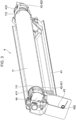
- Fig. 4 is an exploded perspective view illustrating a procedure for assembling the photoconductor unit 4.
- Fig. 4 illustrates the photoconductor drum 11, the housing 41, and the bearings 42 (421, 422).
- Figs. 5 to 7 are perspective views illustrating how the photoconductor unit is assembled.
- the support pieces 411 and 412 of the housing 41 are positioned at the ends of the housing 41.
- the support pieces 411 and 412 are annular portions having cutaway portions in part. More specifically, the support piece 411 has a cutaway portion 413, and the support piece 412 has a cutaway portion 414.
- the cutaway portion 413 of the support piece 411 and the cutaway portion 414 of the support piece 412 are oriented in the same direction.
- the opening lengths of the cutaway portions 413 and 414 of the housing 41 are smaller than the diameter of the photoconductor drum 11.
- the support pieces 411 and 412 have inner peripheral surfaces adapted to the outer diameters of the bearings 421 and 422.
- the support pieces 411 and 412 are deformable and the circumferential lengths of the cutaway portions 413 and 414 are changeable.
- the photoconductor drum 11 is housed in the housing 41 in a lateral direction A by using the cutaway portions 413 and 414 of the support pieces 411 and 412. That is, the one end 111 of the photoconductor drum 11 is inserted into the support piece 411 through the cutaway portion 413 of the support piece 411, and the other end 112 of the photoconductor drum 11 is inserted into the support piece 412 through the cutaway portion 414 of the support piece 412.
- the workability of attaching the photoconductor drum 11 to the housing 41 is improved.
- the lateral direction A is an example of a housing direction.
- the housing direction refers to a direction in which the photoconductor drum 11 is housed in the housing 41 that houses the photoconductor drum 11, and may also refer to a direction in which the photoconductor drum 11 is attached.
- the bearings 421 and 422 are the members that support the photoconductor drum 11.
- the bearing 421 is positioned in the circumferential direction relative to the housing 41 by the support piece 411
- the bearing 422 is positioned in the circumferential direction relative to the housing 41 by the support piece 412.
- the housing 41 includes the support piece 411 serving as a positioning member that positions the bearing 421 relative to the housing 41, and the support piece 412 serving as a positioning member that positions the bearing 422 relative to the housing 41.
- the support piece 411 has the cutaway portion 413, and the support piece 412 has the cutaway portion 414.
- the cutaway portions 413 and 414 are provided at the same position relative to the lateral direction A.
- the support piece 411 is an example of the positioning member that positions the bearing 421 relative to the housing 41.
- member herein refers to, for example, a member in a case where the support piece 411 and the housing 41 are separate members and the support piece 411 is attached to the housing 41, and a member in a case where the support piece 411 is integrated with the housing 41.
- the inner diameter of the support piece 411 does not correspond to the outer diameter of the one end 111 of the photoconductor drum 11. More specifically, the outer diameter of the one end 111 of the photoconductor drum 11 is smaller than the inner diameter of the support piece 411. Therefore, as illustrated in Fig. 5 , the outer peripheral surface of the one end 111 is not in close contact with the inner peripheral surface of the support piece 411, and a clearance G1 is secured in the circumferential direction between the support piece 411 and the one end 111.
- the outer diameter of the other end 112 of the photoconductor drum 11 is smaller than the inner diameter of the support piece 412. Therefore, as illustrated in Fig. 5 , a clearance G2 is secured in the circumferential direction between the support piece 412 and the other end 112.
- the bearing 421 is attached in an axial direction B1 to the one end 111 of the photoconductor drum 11 housed in the housing 41.
- the bearing 422 is attached in an axial direction B2 to the other end 112 of the photoconductor drum 11 housed in the housing 41.
- the photoconductor drum 11 In the state in which the photoconductor drum 11 and the bearings 421 and 422 are housed in the housing 41, the photoconductor drum 11 is rotatably held via the bearings 421 and 422 as illustrated in Fig. 6 .
- the contact member 113 of the photoconductor drum 11 is exposed.
- the contact member 113 is provided for ground (GND) conduction, and is connected to the conduction member 43 (see Fig. 3 ).
- the contact member 113 is detached from the photoconductor drum 11 before the bearing 421 is attached to the one end 111 of the photoconductor drum 11, and is attached to the one end 111 of the photoconductor drum 11 through a through hole 424 (see Fig. 4 ) of the bearing 421 in the axial direction B1 after the bearing 421 is attached to the one end 111 in the axial direction B1.
- the bearing 421 has a cutaway portion 423.
- the cutaway portion 423 is formed to reduce the thickness in the same direction as the axial direction B1 in Fig. 4 .
- the cutaway portion 423 extends in a radial direction from the through hole 424. As illustrated in Fig. 6 , the cutaway portion 423 of the bearing 421 is oriented in the same direction as that of the cutaway portion 413 of the support piece 411.
- the circumferential position of the cutaway portion 423 is substantially the same as that of the cutaway portion 413 of the support piece 411.
- the term “same direction” does not herein mean “totally the same direction,” and may have such a deviation that the workability does not decrease when the contact point 114 is checked by sight through the cutaway portion 423 at the time of assembling.
- the cutaway portion 423 of the bearing 421 is an example of a shape portion.
- the conduction member 43 is attached so that the spring portion 431 comes into contact with the contact point 114 of the contact member 113 as illustrated in Fig. 7 .
- the attachment portion 432 of the conduction member 43 is attached to the housing 41.
- the photoconductor drum 11 and the contact member 113 are examples of an image carrier.
- the cover 44 is attached in the state illustrated in Fig. 7 , thereby obtaining the assembled photoconductor unit 4 illustrated in Fig. 3 . Access to the contact point 114 in the photoconductor unit 4 is described with reference to Fig. 8 .
- Fig. 8 is a perspective view illustrating access to the contact point 114 in the assembled photoconductor unit 4.
- the contact between the spring portion 431 and the contact point 114 may be viewed through the cutaway portion 423 of the bearing 421 in the assembled photoconductor unit 4.
- the cutaway portion 423 of the bearing 421 is oriented in the same direction as that of the cutaway portion 413 of the housing 41. In other words, the cutaway portion 423 of the bearing 421 is oriented in the same direction as the lateral direction A (see Fig. 4 ).
- the contact point may visually be checked without changing the posture of the housing 41 etc. That is, the contact point may be checked by sight in the work of assembling the photoconductor unit 4.
- the attachment and the check by sight may be performed simultaneously.
- the cutaway portion 423 of the bearing 421 be formed so that the contact point 114 (see Fig. 4 ) may be viewed during the assembling work.
- the cutaway portion 423 is provided up to the contact point 114 (see Fig. 4 ). Therefore, erroneous assembling may easily be detected by sight compared with a case where the cutaway portion 423 is not provided up to the contact point 114.
- the cutaway portion 413 of the housing 41 and the cutaway portion 423 of the bearing 421 are oriented in the same direction, that is, in the lateral direction A (see Fig. 4 ) as illustrated in Fig. 8 , but this structure is not limitative.
- the cutaway portion 413 of the housing 41 and the cutaway portion 423 of the bearing 421 may be oriented in different directions within a deviation of, for example, 90 degrees. Even this case, the contact point may visually be checked during the assembling work.
- Figs. 9A and 9B illustrate switching of ground (GND) conduction from ON to OFF when the photoconductor unit 4 is pulled from the body 101 of the image forming apparatus 100.
- Fig. 9A illustrates the photoconductor unit 4 housed in the body 101.
- Fig. 9B illustrates the photoconductor unit 4 pulled from the body 101 to a position where the cutaway portion 423 is not exposed.
- the GND conduction is ON.
- the GND conduction is turned OFF, and the cutaway portion 423 is exposed by further pulling the photoconductor unit 4.
- the GND conduction is turned OFF before the cutaway portion 423 is exposed.
- the user who has pulled the photoconductor unit 4 is not affected even if the user touches the spring portion 431 (see Fig. 7 ) through the cutaway portion 423.
- the GND conduction may mechanically be switched ON and OFF depending on the position of the photoconductor unit 4, or may be switched ON and OFF by control based on detection results from a position sensor.
- the GND conduction is switched OFF to ON in response to insertion of the photoconductor unit 4 into the body 101 to a position where the cutaway portion 423 is not exposed (see Fig. 9B ).
- the contact point may easily be checked compared with a structure in which the contact point is not checkable in an assembled state.
- the workability of checking the contact point at the time of assembling may be increased compared with a case where the shape portion is not oriented in the same direction as the housing direction in which the image carrier is housed in the housing member that houses the image carrier.
- the workability of attaching the photoconductor drum 11 may be improved compared with a case where the positioning member that positions, relative to the housing member, the support member that supports the image carrier is not cut away at the predetermined position relative to the housing direction.
- the visibility for the check on the contact point may be improved compared with a case where the shape portion is not cut away up to the position of the contact point in the direction of the rotation shaft of the image carrier.
- the safety when the image carrier unit is pulled from the image forming apparatus may be improved compared with a case where the conduction member is not configured to, when the image carrier unit is pulled from the image forming apparatus to which the image carrier unit is attached, cut off the electrical conduction of the image carrier before the shape portion is exposed from the image forming apparatus.
- the contact point may easily be checked compared with a structure in which the contact point is not checkable in an assembled state.
Landscapes
- Physics & Mathematics (AREA)
- General Physics & Mathematics (AREA)
- Engineering & Computer Science (AREA)
- Plasma & Fusion (AREA)
- Electrophotography Configuration And Component (AREA)
- Discharging, Photosensitive Material Shape In Electrophotography (AREA)
Abstract
An image carrier unit includes an image carrier configured to carry an image on a surface of the image carrier, a conduction member configured to establish electrical conduction of the image carrier by a contact point with the image carrier, and a shape portion configured to allow viewing of the contact point.
Description
- The present disclosure relates to an image carrier unit and an image forming apparatus.
- For example,
Japanese Unexamined Patent Application Publication No. 2008-57616 - In a process for manufacturing an image carrier unit in which an image carrier that carries an image on its surface is housed in a housing member so that the image carrier is rotatable by a support member, it is necessary to check whether a conduction member for establishing electrical conduction of the image carrier is in contact with the image carrier. If the electrical conduction is not confirmed by a conduction test after assembling, the image carrier unit is disassembled to identify the cause, and whether there is a contact point where the conduction member is in contact with the image carrier is checked. Therefore, the workability decreases. If the contact point is checkable during assembling, it is less likely that the electrical conduction is not confirmed by the conduction test. Therefore, the decrease in workability during the manufacturing process may be suppressed.
- Accordingly, it is an object of the present disclosure to easily check a contact point compared with a structure in which the contact point is not checkable in an assembled state.
- According to a first aspect of the present disclosure, there is provided an image carrier unit comprising: an image carrier configured to carry an image on a surface of the image carrier; a conduction member configured to establish electrical conduction of the image carrier by a contact point with the image carrier; and a shape portion configured to allow viewing of the contact point.
- According to a second aspect of the present disclosure, in the image carrier unit according to the first aspect, the shape portion is oriented in the same direction as a housing direction in which the image carrier is housed in a housing member that houses the image carrier.
- According to a third aspect of the present disclosure, in the image carrier unit according to the second aspect, a positioning member that positions, relative to the housing member, a support member that supports the image carrier is cut away at a predetermined position relative to the housing direction.
- According to a fourth aspect of the present disclosure, in the image carrier unit according to any one of the first to third aspects, the shape portion is cut away up to a position of the contact point in a direction of a rotation shaft of the image carrier.
- According to a fifth aspect of the present disclosure, in the image carrier unit according to any one of the first to fourth aspects, the conduction member is configured to, when the image carrier unit is pulled from an image forming apparatus to which the image carrier unit is attached, cut off the electrical conduction of the image carrier before the shape portion is exposed from the image forming apparatus.
- According to a sixth aspect of the present disclosure, there is provided an image forming apparatus comprising: an image former configured to form an image; and an image carrier unit that constitutes the image former and is insertable into and removable from an apparatus body including the image former. The image carrier unit comprises: an image carrier configured to carry an image on a surface of the image carrier; a conduction member configured to establish electrical conduction of the image carrier by a contact point with the image carrier; and a shape portion configured to allow viewing of the contact point.
- According to the first aspect of the present disclosure, the contact point may easily be checked compared with a structure in which the contact point is not checkable in an assembled state.
- According to the second aspect of the present disclosure, the workability of checking the contact point at the time of assembling may be increased compared with a case where the shape portion is not oriented in the same direction as the housing direction in which the image carrier is housed in the housing member that houses the image carrier.
- According to the third aspect of the present disclosure, the workability of attaching the photoconductor drum may be improved compared with a case where the positioning member that positions, relative to the housing member, the support member that supports the image carrier is not cut away at the predetermined position relative to the housing direction.
- According to the fourth aspect of the present disclosure, the visibility for the check on the contact point may be improved compared with a case where the shape portion is not cut away up to the position of the contact point in the direction of the rotation shaft of the image carrier.
- According to the fifth aspect of the present disclosure, the safety when the image carrier unit is pulled from the image forming apparatus may be improved compared with a case where the conduction member is not configured to, when the image carrier unit is pulled from the image forming apparatus to which the image carrier unit is attached, cut off the electrical conduction of the image carrier before the shape portion is exposed from the image forming apparatus.
- According to the sixth aspect of the present disclosure, the contact point may easily be checked compared with a structure in which the contact point is not checkable in an assembled state.
- An exemplary embodiment of the present disclosure will be described in detail based on the following figures, wherein:
-
Fig. 1 is a schematic structural diagram of an image forming apparatus according to an exemplary embodiment; -
Fig. 2 illustrates the structure of a photoconductor unit; -
Fig. 3 is a perspective view illustrating the photoconductor unit; -
Fig. 4 is an exploded perspective view illustrating a procedure for assembling the photoconductor unit; -
Fig. 5 is a perspective view illustrating how the photoconductor unit is assembled; -
Fig. 6 is a perspective view illustrating how the photoconductor unit is assembled; -
Fig. 7 is a perspective view illustrating how the photoconductor unit is assembled; -
Fig. 8 is a perspective view illustrating access to a contact point in the assembled photoconductor unit; and -
Figs. 9A and 9B illustrate switching of GND conduction from ON to OFF when the photoconductor unit is pulled from the body of the image forming apparatus, in whichFig. 9A illustrates the photoconductor unit housed in the body andFig. 9B illustrates the photoconductor unit pulled from the body to a position where a cutaway portion is not exposed. - An exemplary embodiment of the disclosure is described in detail below with reference to the accompanying drawings. The sizes and thicknesses of components in the drawings to be referred to in the following description may differ from actual dimensions.
-
Fig. 1 is a schematic structural diagram of animage forming apparatus 100 according to this exemplary embodiment. - As illustrated in
Fig. 1 , theimage forming apparatus 100 includes adocument reading device 1 that reads information on a document G, an image former 2 that forms an image on recording paper S based on the information on the document read by the document reading device 1 (read image), and apaper feeder 3 that sends the recording paper S to be fed to the image former 2. In theimage forming apparatus 100, the image former 2 and thepaper feeder 3 are housed in abody 101, and thedocument reading device 1 is disposed above thebody 101. Thebody 101 includes, at its top, anoutput paper receiver 102 that receives the output recording paper S on which the image is formed. - The
document reading device 1 includes ahousing 103. Thedocument reading device 1 includes, at the top of thehousing 103, a lighttransmissive document stage 105 on which the document G is placed, and adocument cover 106 that covers thedocument stage 105 and is openable and closable relative to thehousing 103. Thedocument cover 106 has anautomatic document feeder 107 that transports the document G to a reading position and outputs the read document G, adocument tray 108 on which the document G to be sent by theautomatic document feeder 107 is placed, and areceiver 109 that receives the document G output by theautomatic document feeder 107. - The image former 2 includes an
image forming unit 20 that forms yellow (Y), magenta (M), cyan (C), and black (K) toner images by, for example, an electrophotographic system, anintermediate transfer unit 26 that transports the toner images formed by theimage forming unit 20 until they are transferred onto the recording paper S, and afixing unit 27 that fixes the toner images transferred onto the recording paper S from theintermediate transfer unit 26. - The
image forming unit 20 includesphotoconductor units 4 associated with the individual colors and represented by broken lines. Eachphotoconductor unit 4 is attachable to and removable from thebody 101 by a user. - The
paper feeder 3 includesdrawable containers 31 that contain a plurality of sheets of recording paper S in preset sizes, types, etc., andfeeding devices 32 that send the sheets of recording paper S contained in thecontainers 31 one by one to transport paths. A feeding andtransport path 28 is provided between thepaper feeder 3 and the image former 2 to transport the recording paper S sent from thepaper feeder 3 to a second transfer position. - Next, a basic operation of the
image forming apparatus 100 is described. - In the
document reading device 1, the user places the document G on thedocument stage 105 or thedocument tray 108. When the user operates an operation button (not illustrated) etc. and thedocument reading device 1 receives a document reading instruction, thedocument reading device 1 starts an operation of reading the document G. That is, thedocument reading device 1 acquires read information on the document G. The image former 2 performs an image forming operation based on the read information on the document G received from thedocument reading device 1. In synchronization with the operation of the image former 2, thepaper feeder 3 sends out the recording paper S. After the toner images are fixed by the image former 2, the recording paper S is output to theoutput paper receiver 102. The image forming operation is repeated for the number of documents G or the number of images to be formed. - Next, the
image forming unit 20 according to this exemplary embodiment is described with reference toFig. 2 . More specifically, eachphotoconductor unit 4 constituting theimage forming unit 20 is described. Thephotoconductor unit 4 is an example of an image carrier unit. -
Fig. 2 illustrates the structure of thephotoconductor unit 4 that is viewed from the front side of theimage forming apparatus 100. - As illustrated in
Fig. 2 , thephotoconductor unit 4 includes aphotoconductor drum 11 that rotates in an arrow direction. Thephotoconductor unit 4 includes a chargingroller 12, an exposingdevice 13, a developingdevice 14, atransfer roller 15, and acleaning device 16 as members disposed around thephotoconductor drum 11. Thephotoconductor unit 4 may have all of these members but part of the members may be omitted. - The
photoconductor drum 11 is a cylinder. A photoconductive layer (not illustrated) is formed on the surface of the cylinder. - The charging
roller 12 is a conductive rubber roller etc. and charges thephotoconductor drum 11. - The exposing
device 13 irradiates thephotoconductor drum 11 charged by the chargingroller 12 with light from a laser light source, a light emitting diode (LED) light source, etc. to form an electrostatic latent image on the surface of thephotoconductor drum 11. - The developing
device 14 causes a toner to adhere to the surface of thephotoconductor drum 11 to develop the electrostatic latent image formed on thephotoconductor drum 11 with the toner in a predetermined color. In this way, a toner image is formed on the surface of thephotoconductor drum 11 in this exemplary embodiment. - The developing
device 14 contains a developer. In this exemplary embodiment, the developer is a so-called two-component developer composed of a magnetic carrier and a colored toner. - In this exemplary embodiment, a
developer container 19 contains the developer to be supplied to the developingdevice 14. In this exemplary embodiment, a new developer is supplied from thedeveloper container 19 to the developingdevice 14 through a developer transport path (not illustrated). - The
transfer roller 15 is a conductive rubber roller etc. - In this exemplary embodiment, the
transfer roller 15 and thephotoconductor drum 11 face each other to define a transfer portion T. A transfer bias is applied to thetransfer roller 15. The toner image on the surface of thephotoconductor drum 11, that is, the toner image carried by thephotoconductor drum 11 is transferred onto a belt of theintermediate transfer unit 26 at the transfer portion T. - The
cleaning device 16 includes acontact member 16A disposed in contact with thephotoconductor drum 11, and removes adherents such as a toner on thephotoconductor drum 11. - Next, a specific structure of the
photoconductor unit 4 is described. -
Fig. 3 is a perspective view illustrating thephotoconductor unit 4. - The
photoconductor unit 4 illustrated inFig. 3 includes ahousing 41, bearings 42, aconduction member 43, and acover 44 in addition to thephotoconductor drum 11. - The
housing 41 is a member serving as the body of thephotoconductor unit 4, and supports the members such as thephotoconductor drum 11. More specifically, thehousing 41 includessupport pieces end 111 and anotherend 112 of thephotoconductor drum 11. InFig. 3 , the oneend 111 of thephotoconductor drum 11 is positioned at the left, and theother end 112 of thephotoconductor drum 11 is positioned at the right. - The bearings 42 are resin members provided to the
support pieces housing 41. More specifically, the bearings 42 are a bearing 421 associated with thesupport piece 411, and abearing 422 associated with thesupport piece 412. Thebearings - That is, the
bearing 421 is attached to the oneend 111 of thephotoconductor drum 11 at thesupport piece 411, and thebearing 422 is attached to theother end 112 of thephotoconductor drum 11 at thesupport piece 412. - In this way, the one
end 111 of thephotoconductor drum 11 is rotatably supported by thesupport piece 411 via thebearing 421, and theother end 112 of thephotoconductor drum 11 is rotatably supported by thesupport piece 412 via thebearing 422. - The
bearing 421 is an example of a support member. Thehousing 41 is an example of a housing member and an example of a positioning member. - The
conduction member 43 is a wire in contact with a contact member 113 (seeFig. 4 ) of thephotoconductor drum 11 for ground (GND) conduction. In this exemplary embodiment, theconduction member 43 is provided near the oneend 111 of the photoconductor drum 11 (left inFig. 3 ). - The
conduction member 43 includes a spring portion 431 (seeFig. 7 ) in contact with a contact point 114 (seeFig. 4 ) of thecontact member 113, and anattachment portion 432 attached to thehousing 41. - The
cover 44 is a resin member that covers thespring portion 431 of theconduction member 43. Thecover 44 is provided near thesupport piece 411 of thehousing 41 where theconduction member 43 is provided, but may be provided near thesupport piece 412. - The structure of the
photoconductor unit 4 according to this exemplary embodiment is described below with reference toFigs. 4 to 7 . -
Fig. 4 is an exploded perspective view illustrating a procedure for assembling thephotoconductor unit 4.Fig. 4 illustrates thephotoconductor drum 11, thehousing 41, and the bearings 42 (421, 422).Figs. 5 to 7 are perspective views illustrating how the photoconductor unit is assembled. - As illustrated in
Fig. 4 , thesupport pieces housing 41 are positioned at the ends of thehousing 41. Thesupport pieces support piece 411 has acutaway portion 413, and thesupport piece 412 has acutaway portion 414. Thecutaway portion 413 of thesupport piece 411 and thecutaway portion 414 of thesupport piece 412 are oriented in the same direction. - The opening lengths of the
cutaway portions housing 41 are smaller than the diameter of thephotoconductor drum 11. Thesupport pieces bearings support pieces cutaway portions - The
photoconductor drum 11 is housed in thehousing 41 in a lateral direction A by using thecutaway portions support pieces end 111 of thephotoconductor drum 11 is inserted into thesupport piece 411 through thecutaway portion 413 of thesupport piece 411, and theother end 112 of thephotoconductor drum 11 is inserted into thesupport piece 412 through thecutaway portion 414 of thesupport piece 412. Thus, the workability of attaching thephotoconductor drum 11 to thehousing 41 is improved. - The lateral direction A is an example of a housing direction. The housing direction refers to a direction in which the
photoconductor drum 11 is housed in thehousing 41 that houses thephotoconductor drum 11, and may also refer to a direction in which thephotoconductor drum 11 is attached. - As described above, the
bearings photoconductor drum 11. Thebearing 421 is positioned in the circumferential direction relative to thehousing 41 by thesupport piece 411, and thebearing 422 is positioned in the circumferential direction relative to thehousing 41 by thesupport piece 412. In other words, thehousing 41 includes thesupport piece 411 serving as a positioning member that positions thebearing 421 relative to thehousing 41, and thesupport piece 412 serving as a positioning member that positions thebearing 422 relative to thehousing 41. - The
support piece 411 has thecutaway portion 413, and thesupport piece 412 has thecutaway portion 414. Thecutaway portions - As described above, the
support piece 411 is an example of the positioning member that positions thebearing 421 relative to thehousing 41. The term "member" herein refers to, for example, a member in a case where thesupport piece 411 and thehousing 41 are separate members and thesupport piece 411 is attached to thehousing 41, and a member in a case where thesupport piece 411 is integrated with thehousing 41. - Focusing on the
support piece 411 of thehousing 41, the inner diameter of thesupport piece 411 does not correspond to the outer diameter of the oneend 111 of thephotoconductor drum 11. More specifically, the outer diameter of the oneend 111 of thephotoconductor drum 11 is smaller than the inner diameter of thesupport piece 411. Therefore, as illustrated inFig. 5 , the outer peripheral surface of the oneend 111 is not in close contact with the inner peripheral surface of thesupport piece 411, and a clearance G1 is secured in the circumferential direction between thesupport piece 411 and the oneend 111. - The same applies to the
support piece 412 of thehousing 41. The outer diameter of theother end 112 of thephotoconductor drum 11 is smaller than the inner diameter of thesupport piece 412. Therefore, as illustrated inFig. 5 , a clearance G2 is secured in the circumferential direction between thesupport piece 412 and theother end 112. - The description is continued referring back to
Fig. 4 . Thebearing 421 is attached in an axial direction B1 to the oneend 111 of thephotoconductor drum 11 housed in thehousing 41. Similarly, thebearing 422 is attached in an axial direction B2 to theother end 112 of thephotoconductor drum 11 housed in thehousing 41. - In the state in which the
photoconductor drum 11 and thebearings housing 41, thephotoconductor drum 11 is rotatably held via thebearings Fig. 6 . - Referring to
Fig. 6 , thecontact member 113 of thephotoconductor drum 11 is exposed. As described above, thecontact member 113 is provided for ground (GND) conduction, and is connected to the conduction member 43 (seeFig. 3 ). - The
contact member 113 is detached from thephotoconductor drum 11 before thebearing 421 is attached to the oneend 111 of thephotoconductor drum 11, and is attached to the oneend 111 of thephotoconductor drum 11 through a through hole 424 (seeFig. 4 ) of thebearing 421 in the axial direction B1 after thebearing 421 is attached to the oneend 111 in the axial direction B1. - As illustrated in
Fig. 4 , thebearing 421 has acutaway portion 423. Thecutaway portion 423 is formed to reduce the thickness in the same direction as the axial direction B1 inFig. 4 . - The
cutaway portion 423 extends in a radial direction from the throughhole 424. As illustrated inFig. 6 , thecutaway portion 423 of thebearing 421 is oriented in the same direction as that of thecutaway portion 413 of thesupport piece 411. - More specifically, when the
bearing 421 is positioned relative to thehousing 41, the circumferential position of thecutaway portion 423 is substantially the same as that of thecutaway portion 413 of thesupport piece 411. - The term "same direction" does not herein mean "totally the same direction," and may have such a deviation that the workability does not decrease when the
contact point 114 is checked by sight through thecutaway portion 423 at the time of assembling. Thecutaway portion 423 of thebearing 421 is an example of a shape portion. - In the state in which the
photoconductor drum 11 and thebearings housing 41, theconduction member 43 is attached so that thespring portion 431 comes into contact with thecontact point 114 of thecontact member 113 as illustrated inFig. 7 . Theattachment portion 432 of theconduction member 43 is attached to thehousing 41. - The
photoconductor drum 11 and thecontact member 113 are examples of an image carrier. - The
cover 44 is attached in the state illustrated inFig. 7 , thereby obtaining the assembledphotoconductor unit 4 illustrated inFig. 3 . Access to thecontact point 114 in thephotoconductor unit 4 is described with reference toFig. 8 . -
Fig. 8 is a perspective view illustrating access to thecontact point 114 in the assembledphotoconductor unit 4. - As illustrated in
Fig. 8 , the contact between thespring portion 431 and thecontact point 114 may be viewed through thecutaway portion 423 of thebearing 421 in the assembledphotoconductor unit 4. - In the work of assembling the
photoconductor unit 4, thecutaway portion 423 of thebearing 421 is oriented in the same direction as that of thecutaway portion 413 of thehousing 41. In other words, thecutaway portion 423 of thebearing 421 is oriented in the same direction as the lateral direction A (seeFig. 4 ). - Thus, in the work of assembling the
photoconductor unit 4, the contact point may visually be checked without changing the posture of thehousing 41 etc. That is, the contact point may be checked by sight in the work of assembling thephotoconductor unit 4. - Since the direction in which the
photoconductor drum 11 is attached to thehousing 41 agrees with the direction in which thecutaway portion 423 of thebearing 421 is oriented, the attachment and the check by sight may be performed simultaneously. - It is appropriate that the
cutaway portion 423 of thebearing 421 be formed so that the contact point 114 (seeFig. 4 ) may be viewed during the assembling work. In this exemplary embodiment, thecutaway portion 423 is provided up to the contact point 114 (seeFig. 4 ). Therefore, erroneous assembling may easily be detected by sight compared with a case where thecutaway portion 423 is not provided up to thecontact point 114. - In this exemplary embodiment, the
cutaway portion 413 of thehousing 41 and thecutaway portion 423 of thebearing 421 are oriented in the same direction, that is, in the lateral direction A (seeFig. 4 ) as illustrated inFig. 8 , but this structure is not limitative. Thecutaway portion 413 of thehousing 41 and thecutaway portion 423 of thebearing 421 may be oriented in different directions within a deviation of, for example, 90 degrees. Even this case, the contact point may visually be checked during the assembling work. -
Figs. 9A and 9B illustrate switching of ground (GND) conduction from ON to OFF when thephotoconductor unit 4 is pulled from thebody 101 of theimage forming apparatus 100.Fig. 9A illustrates thephotoconductor unit 4 housed in thebody 101.Fig. 9B illustrates thephotoconductor unit 4 pulled from thebody 101 to a position where thecutaway portion 423 is not exposed. - In the state in which the
photoconductor unit 4 is housed in thebody 101 as illustrated inFig. 9A , the GND conduction is ON. When thephotoconductor unit 4 is pulled from thebody 101 as illustrated inFig. 9B , the GND conduction is turned OFF, and thecutaway portion 423 is exposed by further pulling thephotoconductor unit 4. - In this exemplary embodiment, when the
photoconductor unit 4 is pulled from thebody 101, the GND conduction is turned OFF before thecutaway portion 423 is exposed. Thus, the user who has pulled thephotoconductor unit 4 is not affected even if the user touches the spring portion 431 (seeFig. 7 ) through thecutaway portion 423. - The GND conduction may mechanically be switched ON and OFF depending on the position of the
photoconductor unit 4, or may be switched ON and OFF by control based on detection results from a position sensor. - When the
photoconductor unit 4 is attached to thebody 101 of theimage forming apparatus 100, the GND conduction is switched OFF to ON in response to insertion of thephotoconductor unit 4 into thebody 101 to a position where thecutaway portion 423 is not exposed (seeFig. 9B ). - The foregoing description of the exemplary embodiments of the present disclosure has been provided for the purposes of illustration and description. It is not intended to be exhaustive or to limit the disclosure to the precise forms disclosed. Obviously, many modifications and variations will be apparent to practitioners skilled in the art. The exemplary embodiments were chosen and described in order to best explain the principles of the disclosure and its practical applications, thereby enabling others skilled in the art to understand the disclosure for various exemplary embodiments and with the various modifications as are suited to the particular use contemplated. It is intended that the scope of the disclosure be defined by the following claims and their equivalents.
-
- (((1))) An image carrier unit comprising:
- an image carrier configured to carry an image on a surface of the image carrier;
- a conduction member configured to establish electrical conduction of the image carrier by a contact point with the image carrier; and
- a shape portion configured to allow viewing of the contact point.
- (((2))) The image carrier unit according to (((1))), wherein the shape portion is oriented in the same direction as a housing direction in which the image carrier is housed in a housing member that houses the image carrier.
- (((3))) The image carrier unit according to (((2))), wherein a positioning member that positions, relative to the housing member, a support member that supports the image carrier is cut away at a predetermined position relative to the housing direction.
- (((4))) The image carrier unit according to any one of (((1))) to (((3))), wherein the shape portion is cut away up to a position of the contact point in a direction of a rotation shaft of the image carrier.
- (((5))) The image carrier unit according to any one of (((1))) to (((4))), wherein the conduction member is configured to, when the image carrier unit is pulled from an image forming apparatus to which the image carrier unit is attached, cut off the electrical conduction of the image carrier before the shape portion is exposed from the image forming apparatus.
- (((6))) An image forming apparatus comprising:
- an image former configured to form an image; and
- an image carrier unit that constitutes the image former and is insertable into and removable from an apparatus body including the image former,
- wherein the image carrier unit comprises:
- an image carrier configured to carry an image on a surface of the image carrier;
- a conduction member configured to establish electrical conduction of the image carrier by a contact point with the image carrier; and
- a shape portion configured to allow viewing of the contact point.
- According to (((1))), the contact point may easily be checked compared with a structure in which the contact point is not checkable in an assembled state.
- According to (((2))), the workability of checking the contact point at the time of assembling may be increased compared with a case where the shape portion is not oriented in the same direction as the housing direction in which the image carrier is housed in the housing member that houses the image carrier.
- According to (((3))), the workability of attaching the
photoconductor drum 11 may be improved compared with a case where the positioning member that positions, relative to the housing member, the support member that supports the image carrier is not cut away at the predetermined position relative to the housing direction. - According to (((4))), the visibility for the check on the contact point may be improved compared with a case where the shape portion is not cut away up to the position of the contact point in the direction of the rotation shaft of the image carrier.
- According to (((5))), the safety when the image carrier unit is pulled from the image forming apparatus may be improved compared with a case where the conduction member is not configured to, when the image carrier unit is pulled from the image forming apparatus to which the image carrier unit is attached, cut off the electrical conduction of the image carrier before the shape portion is exposed from the image forming apparatus.
- According to (((6))), the contact point may easily be checked compared with a structure in which the contact point is not checkable in an assembled state.
Claims (6)
- An image carrier unit comprising:an image carrier configured to carry an image on a surface of the image carrier;a conduction member configured to establish electrical conduction of the image carrier by a contact point with the image carrier; anda shape portion configured to allow viewing of the contact point.
- The image carrier unit according to claim 1, wherein the shape portion is oriented in the same direction as a housing direction in which the image carrier is housed in a housing member that houses the image carrier.
- The image carrier unit according to claim 2, wherein a positioning member that positions, relative to the housing member, a support member that supports the image carrier is cut away at a predetermined position relative to the housing direction.
- The image carrier unit according to any one of claims 1 to 3, wherein the shape portion is cut away up to a position of the contact point in a direction of a rotation shaft of the image carrier.
- The image carrier unit according to any one of claims 1 to 4, wherein the conduction member is configured to, when the image carrier unit is pulled from an image forming apparatus to which the image carrier unit is attached, cut off the electrical conduction of the image carrier before the shape portion is exposed from the image forming apparatus.
- An image forming apparatus comprising:an image former configured to form an image; andan image carrier unit that constitutes the image former and is insertable into and removable from an apparatus body including the image former,wherein the image carrier unit comprises:an image carrier configured to carry an image on a surface of the image carrier;a conduction member configured to establish electrical conduction of the image carrier by a contact point with the image carrier; anda shape portion configured to allow viewing of the contact point.
Applications Claiming Priority (1)
| Application Number | Priority Date | Filing Date | Title |
|---|---|---|---|
| JP2023116036A JP2025012871A (en) | 2023-07-14 | 2023-07-14 | Image carrier unit and image forming apparatus |
Publications (1)
| Publication Number | Publication Date |
|---|---|
| EP4492148A1 true EP4492148A1 (en) | 2025-01-15 |
Family
ID=89854586
Family Applications (1)
| Application Number | Title | Priority Date | Filing Date |
|---|---|---|---|
| EP24156183.6A Pending EP4492148A1 (en) | 2023-07-14 | 2024-02-07 | Image carrier unit and image forming apparatus |
Country Status (4)
| Country | Link |
|---|---|
| US (1) | US12326671B2 (en) |
| EP (1) | EP4492148A1 (en) |
| JP (1) | JP2025012871A (en) |
| CN (1) | CN119310815A (en) |
Citations (2)
| Publication number | Priority date | Publication date | Assignee | Title |
|---|---|---|---|---|
| JP2008057616A (en) | 2006-08-30 | 2008-03-13 | Canon Finetech Inc | Rotating shaft support device |
| US20090220275A1 (en) * | 2008-02-29 | 2009-09-03 | Brother Kogyo Kabushiki Kaisha | Tandem Type Photosensitive Unit and Image Forming Apparatus |
Family Cites Families (3)
| Publication number | Priority date | Publication date | Assignee | Title |
|---|---|---|---|---|
| JP3285392B2 (en) * | 1992-09-04 | 2002-05-27 | キヤノン株式会社 | Process cartridge and image forming apparatus |
| JP3885062B2 (en) * | 2004-03-30 | 2007-02-21 | キヤノン株式会社 | Electrophotographic photosensitive drum, process cartridge, and electrophotographic image forming apparatus |
| JP4455124B2 (en) * | 2004-03-31 | 2010-04-21 | キヤノン株式会社 | Electrophotographic image forming apparatus |
-
2023
- 2023-07-14 JP JP2023116036A patent/JP2025012871A/en active Pending
-
2024
- 2024-02-05 US US18/432,298 patent/US12326671B2/en active Active
- 2024-02-05 CN CN202410161752.XA patent/CN119310815A/en active Pending
- 2024-02-07 EP EP24156183.6A patent/EP4492148A1/en active Pending
Patent Citations (2)
| Publication number | Priority date | Publication date | Assignee | Title |
|---|---|---|---|---|
| JP2008057616A (en) | 2006-08-30 | 2008-03-13 | Canon Finetech Inc | Rotating shaft support device |
| US20090220275A1 (en) * | 2008-02-29 | 2009-09-03 | Brother Kogyo Kabushiki Kaisha | Tandem Type Photosensitive Unit and Image Forming Apparatus |
Also Published As
| Publication number | Publication date |
|---|---|
| US12326671B2 (en) | 2025-06-10 |
| US20250021031A1 (en) | 2025-01-16 |
| JP2025012871A (en) | 2025-01-24 |
| CN119310815A (en) | 2025-01-14 |
Similar Documents
| Publication | Publication Date | Title |
|---|---|---|
| JP4126254B2 (en) | Image forming apparatus | |
| US7386241B2 (en) | Processing cartridge rotating a drum shaft in different directions and image forming apparatus mounting such a cartridge | |
| JP2004086182A (en) | Process cartridge and electrophotographic image forming apparatus | |
| US8909070B2 (en) | Image forming apparatus and cartridge | |
| JP2013174652A (en) | cartridge | |
| JP5769126B2 (en) | Image forming apparatus | |
| US12326671B2 (en) | Image carrier unit and image forming apparatus | |
| JP2008286899A (en) | Heat roller and fixing device equipped therewith | |
| JP2017207565A (en) | Rotation driving device and image forming apparatus | |
| US8554109B2 (en) | Image forming apparatus | |
| US8699927B2 (en) | Development device and image forming apparatus | |
| JP7528346B2 (en) | Manufacturing method of developing device | |
| JP2021162781A (en) | Drum unit | |
| JP2021015234A (en) | Image forming apparatus | |
| JP6658630B2 (en) | Image forming apparatus and developing unit | |
| EP3913438B1 (en) | Developing device and image forming apparatus | |
| JP2013011709A (en) | Photosensitive drum and image forming apparatus including the same | |
| US10067462B2 (en) | Developer container, developer unit and image forming apparatus | |
| US20180259901A1 (en) | Developer carrier, developing device, and image forming apparatus | |
| US9891582B2 (en) | Process unit and image forming apparatus provided with the same | |
| JP7748614B2 (en) | Developing device, process cartridge, and image forming apparatus | |
| JP5551017B2 (en) | Bearing support unit and image forming apparatus | |
| JP6256324B2 (en) | Developing device and image forming apparatus | |
| JP4791847B2 (en) | Developing device and image forming apparatus | |
| JP6972805B2 (en) | Image holder, image forming unit, image forming device |
Legal Events
| Date | Code | Title | Description |
|---|---|---|---|
| PUAI | Public reference made under article 153(3) epc to a published international application that has entered the european phase |
Free format text: ORIGINAL CODE: 0009012 |
|
| STAA | Information on the status of an ep patent application or granted ep patent |
Free format text: STATUS: THE APPLICATION HAS BEEN PUBLISHED |
|
| AK | Designated contracting states |
Kind code of ref document: A1 Designated state(s): AL AT BE BG CH CY CZ DE DK EE ES FI FR GB GR HR HU IE IS IT LI LT LU LV MC ME MK MT NL NO PL PT RO RS SE SI SK SM TR |
|
| STAA | Information on the status of an ep patent application or granted ep patent |
Free format text: STATUS: REQUEST FOR EXAMINATION WAS MADE |
|
| 17P | Request for examination filed |
Effective date: 20250313 |