EP4489308A1 - Analog-to-digital converter, analog-to-digital conversion system, digital control device, and digital control power source - Google Patents
Analog-to-digital converter, analog-to-digital conversion system, digital control device, and digital control power source Download PDFInfo
- Publication number
- EP4489308A1 EP4489308A1 EP22929804.7A EP22929804A EP4489308A1 EP 4489308 A1 EP4489308 A1 EP 4489308A1 EP 22929804 A EP22929804 A EP 22929804A EP 4489308 A1 EP4489308 A1 EP 4489308A1
- Authority
- EP
- European Patent Office
- Prior art keywords
- signal
- circuit
- digital
- converter
- analog
- Prior art date
- Legal status (The legal status is an assumption and is not a legal conclusion. Google has not performed a legal analysis and makes no representation as to the accuracy of the status listed.)
- Pending
Links
Images


Classifications
-
- H—ELECTRICITY
- H03—ELECTRONIC CIRCUITRY
- H03M—CODING; DECODING; CODE CONVERSION IN GENERAL
- H03M3/00—Conversion of analogue values to or from differential modulation
- H03M3/30—Delta-sigma modulation
- H03M3/39—Structural details of delta-sigma modulators, e.g. incremental delta-sigma modulators
- H03M3/436—Structural details of delta-sigma modulators, e.g. incremental delta-sigma modulators characterised by the order of the loop filter, e.g. error feedback type
- H03M3/438—Structural details of delta-sigma modulators, e.g. incremental delta-sigma modulators characterised by the order of the loop filter, e.g. error feedback type the modulator having a higher order loop filter in the feedforward path
-
- H—ELECTRICITY
- H03—ELECTRONIC CIRCUITRY
- H03M—CODING; DECODING; CODE CONVERSION IN GENERAL
- H03M1/00—Analogue/digital conversion; Digital/analogue conversion
- H03M1/12—Analogue/digital converters
- H03M1/18—Automatic control for modifying the range of signals the converter can handle, e.g. gain ranging
- H03M1/181—Automatic control for modifying the range of signals the converter can handle, e.g. gain ranging in feedback mode, i.e. by determining the range to be selected from one or more previous digital output values
-
- H—ELECTRICITY
- H03—ELECTRONIC CIRCUITRY
- H03M—CODING; DECODING; CODE CONVERSION IN GENERAL
- H03M1/00—Analogue/digital conversion; Digital/analogue conversion
- H03M1/10—Calibration or testing
- H03M1/1071—Measuring or testing
-
- H—ELECTRICITY
- H03—ELECTRONIC CIRCUITRY
- H03M—CODING; DECODING; CODE CONVERSION IN GENERAL
- H03M1/00—Analogue/digital conversion; Digital/analogue conversion
- H03M1/12—Analogue/digital converters
- H03M1/34—Analogue value compared with reference values
-
- H—ELECTRICITY
- H03—ELECTRONIC CIRCUITRY
- H03M—CODING; DECODING; CODE CONVERSION IN GENERAL
- H03M3/00—Conversion of analogue values to or from differential modulation
- H03M3/30—Delta-sigma modulation
- H03M3/322—Continuously compensating for, or preventing, undesired influence of physical parameters
- H03M3/324—Continuously compensating for, or preventing, undesired influence of physical parameters characterised by means or methods for compensating or preventing more than one type of error at a time, e.g. by synchronisation or using a ratiometric arrangement
- H03M3/35—Continuously compensating for, or preventing, undesired influence of physical parameters characterised by means or methods for compensating or preventing more than one type of error at a time, e.g. by synchronisation or using a ratiometric arrangement using redundancy
-
- H—ELECTRICITY
- H03—ELECTRONIC CIRCUITRY
- H03M—CODING; DECODING; CODE CONVERSION IN GENERAL
- H03M3/00—Conversion of analogue values to or from differential modulation
- H03M3/30—Delta-sigma modulation
- H03M3/378—Testing
-
- H—ELECTRICITY
- H03—ELECTRONIC CIRCUITRY
- H03M—CODING; DECODING; CODE CONVERSION IN GENERAL
- H03M3/00—Conversion of analogue values to or from differential modulation
- H03M3/30—Delta-sigma modulation
- H03M3/39—Structural details of delta-sigma modulators, e.g. incremental delta-sigma modulators
- H03M3/412—Structural details of delta-sigma modulators, e.g. incremental delta-sigma modulators characterised by the number of quantisers and their type and resolution
- H03M3/42—Structural details of delta-sigma modulators, e.g. incremental delta-sigma modulators characterised by the number of quantisers and their type and resolution having multiple quantisers arranged in parallel loops
-
- H—ELECTRICITY
- H03—ELECTRONIC CIRCUITRY
- H03M—CODING; DECODING; CODE CONVERSION IN GENERAL
- H03M3/00—Conversion of analogue values to or from differential modulation
- H03M3/30—Delta-sigma modulation
- H03M3/39—Structural details of delta-sigma modulators, e.g. incremental delta-sigma modulators
- H03M3/412—Structural details of delta-sigma modulators, e.g. incremental delta-sigma modulators characterised by the number of quantisers and their type and resolution
- H03M3/422—Structural details of delta-sigma modulators, e.g. incremental delta-sigma modulators characterised by the number of quantisers and their type and resolution having one quantiser only
- H03M3/43—Structural details of delta-sigma modulators, e.g. incremental delta-sigma modulators characterised by the number of quantisers and their type and resolution having one quantiser only the quantiser being a single bit one
-
- H—ELECTRICITY
- H03—ELECTRONIC CIRCUITRY
- H03M—CODING; DECODING; CODE CONVERSION IN GENERAL
- H03M3/00—Conversion of analogue values to or from differential modulation
- H03M3/30—Delta-sigma modulation
- H03M3/458—Analogue/digital converters using delta-sigma modulation as an intermediate step
Definitions
- the present disclosure relates to an analog/digital converter, an analog/digital conversion system, a digital control device, and a digital control power supply.
- a technique disclosed, for example, in Japanese Patent Laying-Open No.2019-057937 has been known as a technique to enhance conversion accuracy with an inexpensive circuit configuration in a ⁇ type analog/digital (A/D) converter.
- a ⁇ modulation unit includes a first ⁇ modulation unit an input voltage to which has a voltage value of a voltage to be inspected and a second ⁇ modulation unit an input voltage to which has a voltage value of a correction reference voltage.
- a digital filter unit is provided with a first digital filter to generate N-bit data based on information indicated by 1-bit data generated by the first ⁇ modulation unit and a second digital filter to generate N-bit data based on information indicated by 1-bit data generated by the second ⁇ modulation unit.
- a correction computing unit performs correction computation of the N-bit data created by the first digital filter with the N-bit data created by the second digital filter (see the Abstract of PTL 1).
- a resistive element R1 and a capacitor C1 perform a function of a smoothing circuit, a function of a delay DA conversion circuit, and a function of an integration circuit (see paragraphs [0018] and [0019] of PTL 1).
- the present disclosure was made in view of the background art above, and one of objects thereof is to provide a ⁇ type A/D converter capable of achieving conversion accuracy higher than in a conventional technique with an inexpensive circuit configuration. Other objects and features of the present disclosure will be described in embodiments below.
- An analog/digital converter in one embodiment includes a first integration circuit, a second integration circuit, and a first signal generation circuit.
- the first integration circuit temporally integrates a sum of an analog input signal and a first feedback signal and includes an active element.
- the second integration circuit temporally integrates a sum of a result of integration by the first integration circuit and the first feedback signal and does not include an active element.
- the first signal generation circuit compares a first output voltage representing a result of integration by the second integration circuit with a threshold voltage at discrete time intervals.
- the first signal generation circuit generates 1 as a first digital signal when the first output voltage is higher than the threshold voltage and generates 0 as the first digital signal when the first output voltage is lower than the threshold voltage.
- the first signal generation circuit outputs a signal obtained by inversion of 1 and 0 of the first digital signal as the first feedback signal.
- a secondary ⁇ type analog/digital converter can be configured with the first integration circuit including the active element and the second integration circuit not including the active element, and hence conversion accuracy can be higher than in the conventional technique with an inexpensive circuit configuration.
- Fig. 1 is a circuit diagram showing a configuration of a ⁇ type A/D converter 90 according to a first embodiment.
- ⁇ type A/D converter 90 according to the first embodiment includes an analog circuit portion (10 and 20) and a digital circuit 30.
- the analog circuit portion (10 and 20) includes an integration circuit 10 including an active element and an integration circuit 20 configured with a passive circuit and not including an active element.
- the active element refers to a semiconductor amplifier and the like configured with an operational amplifier or a discrete component.
- Integration circuit 10 will also be referred to as an active integration circuit 10 or a first integration circuit 10 below and integration circuit 20 will also be referred to as a passive integration circuit 20 or a second integration circuit 20 below.
- a configuration of each of circuits 10 to 30 and connection between constituent elements included in each circuit will initially be described.
- Active integration circuit 10 is configured to temporally integrate a sum of an input signal Vin and a digital signal fed back from digital circuit 30 to active integration circuit 10. As shown in Fig. 1 , active integration circuit 10 includes resistive elements 11 to 14, capacitors 15 and 16, and a semiconductor amplifier 17. Semiconductor amplifier 17 is an operational amplifier including a non-inverting input terminal (a + terminal), an inverting input terminal (a - terminal), and an output terminal.
- Resistive element 11 is connected between a node to which input signal Vin is inputted and the non-inverting input terminal of semiconductor amplifier 17.
- Resistive element 12 is connected between a node 24 on an output side of a buffer element 33 which will be described later and the non-inverting input terminal of semiconductor amplifier 17.
- Capacitor 16 is connected between the non-inverting input terminal of semiconductor amplifier 17 and a ground GND.
- Resistive element 13 is connected between the inverting input terminal of semiconductor amplifier 17 and ground GND.
- Resistive element 14 is connected between the inverting input terminal of semiconductor amplifier 17 and a node to which a reference voltage Vref is supplied.
- Capacitor 15 is connected between the inverting input terminal and the output terminal of semiconductor amplifier 17.
- Passive integration circuit 20 is configured to temporally integrate a sum of the output signal from active integration circuit 10 and a digital signal fed back from digital circuit 30 to passive integration circuit 20.
- passive integration circuit 20 includes resistive elements 21 and 22 and a capacitor 23. Resistive element 22 and capacitor 23 are connected in series in this order between node 24 on the output side of buffer element 33 and ground GND. Resistive element 21 is connected between the output terminal of semiconductor amplifier 17 of active integration circuit 10 and a connection node 25 between resistive element 22 and capacitor 23.
- Digital circuit 30 compares an output voltage V5 from passive integration circuit 20 with a threshold voltage Vth at discrete time intervals (specifically, every cycle of a clock signal CLK). When output voltage V5 is higher than threshold voltage Vth, digital circuit 30 feeds a digital signal "0" back to analog circuit portions 10 and 20, and when output voltage V5 is lower than threshold voltage Vth, digital circuit 30 feeds a digital signal "1" back to analog circuit portions 10 and 20. Digital circuit 30 may be configured to feed “0” or “1” back when output voltage V5 is equal to threshold voltage Vth. As shown in Fig. 1 , digital circuit 30 includes a differential input buffer element 31, a D flip-flop 32, buffer element 33 for inverted output, and a low pass filter (LPF) 35.
- LPF low pass filter
- Buffer element 31 has a non-inverting input terminal connected to connection node 25 of passive integration circuit 20. Threshold voltage Vth is inputted to an inverting input terminal of buffer element 31. An output signal from buffer element 31 is inputted to a D terminal of D flip-flop 32. A digital signal DS outputted from a Q terminal of D flip-flop 32 is inputted to low pass filter 35 and to buffer element 33. Clock signal CLK is inputted to a clock terminal of D flip-flop 32. Buffer element 33 outputs a signal obtained by inversion of 0/1 of inputted digital signal DS to one end of resistive element 12 and one end of resistive element 22.
- buffer elements 31 and 33 and D flip-flop 32 are collectively referred to as a signal generation circuit 34.
- Signal generation circuit 34 generates digital signal DS in accordance with input signal Vin and outputs a signal obtained by inversion of 0/1 of digital signal DS as a feedback signal to active integration circuit 10 and passive integration circuit 20.
- Active integration circuit 10, passive integration circuit 20, and signal generation circuit 34 implement what is called a ⁇ modulator 91.
- Low pass filter 35 removes quantization noise shifted into a high frequency domain by a noise shaping function of ⁇ modulator 91. Consequently, a highly accurate digital signal Dout in proportion to analog input signal Vin is outputted from ⁇ type A/D converter 90. Instead of the low pass filter, processing for counting a ratio of 0 or 1 in digital signal DS outputted from signal generation circuit 34 may be performed.
- Digital circuit 30 can also be configured with an individual semiconductor element, or with a programmable logic device or a microprocessor.
- a field programmable gate array (FPGA) which is one type of the programmable logic device often includes a differential input buffer, and it is suitable for highly integrated mount of a large number of A/D conversion circuits and other digital circuits.
- reference voltage Vref When reference voltage Vref is set to be equal to a supply voltage of buffer element 33 in Fig. 1 , this voltage serves as the reference voltage of the A/D converter. In addition, when threshold voltage Vth is set to 1/2 of reference voltage Vref, circuit operations are suitably symmetrical.
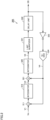
- Fig. 2 is a functional block diagram of a secondary ⁇ modulator 300 corresponding to ⁇ type A/D converter 90 in Fig. 1 .
- ⁇ modulator 300 includes integrators 310 and 320, adders 311 and 321, a 1-bit quantizer 331, a delay unit 332, a buffer element 333 for inverted output, and a 1-bit digital-to-analog converter (DAC) 334.
- DAC digital-to-analog converter
- buffer element 333 for inverted output is not provided in a stage immediately subsequent to delay unit 332, a subtractor should be provided instead of each of adders 311 and 321.
- the present embodiment is characterized in that an adder can be employed instead of a subtractor, by providing buffer element 333.
- Adder 311 adds a feedback signal V4 to input signal Vin (an input voltage V1). Integrator 310 temporally integrates results of addition by adder 311. Adder 321 adds feedback signal V4 to a voltage V3 representing a result of integration by integrator 310. Integrator 320 temporally integrates results of addition by adder 321.
- One-bit quantizer 331 compares voltage V5 representing a result of integration by integrator 320 with threshold voltage Vth to convert the voltage into a binary digital signal.
- Delay unit 332 generates digital signal DS by delaying an output from 1-bit quantizer 331 by one clock cycle. Buffer element 333 inverts 0/1 of digital signal DS outputted from delay unit 332.
- Digital/analog converter 334 generates feedback signal V4 by converting the inverted digital signal outputted from buffer element 333 into an analog signal.
- Each functional block in Fig. 2 is associated with the circuit in Fig. 1 as below.
- adder 311 and integrator 310 in Fig. 2 correspond to active integration circuit 10 in Fig. 1 .
- Adder 321 and integrator 320 in Fig. 2 correspond to passive integration circuit 20 in Fig. 1 .
- One-bit quantizer 331 in Fig. 2 corresponds to differential input buffer element 31 in Fig. 1 .
- Delay unit 332 in Fig. 2 corresponds to D flip-flop 32 in Fig. 1 .
- Buffer element 333 and digital/analog converter 334 in Fig. 2 correspond to buffer element 33 in Fig. 1 .
- the digital signal "0" is defined as a Low level and the digital signal "1" is defined as a High level.
- a negative feedback circuit necessary for ⁇ type A/D converter 90 can thus be configured without a subtractor, and simplified passive integration circuit 20 can be employed for integrator 320 in a second stage.
- the digital signal "0" fed back from digital circuit 30 may be defined as the High level and the digital signal "1" may be defined as the Low level, analog circuit portions 10 and 20 should perform a subtraction function in that case.
- active integration circuit 10 resistance values of resistive elements 11 and 13 are denoted as Ri1
- resistance values of resistive elements 12 and 14 are denoted as Rf1
- capacitance values of capacitors 15 and 16 are denoted as Ci1.
- V2 V 4 ⁇ Vref
- a transfer function of active integration circuit 10 is represented as below, based on a condition of virtual short of the operational amplifier implemented by semiconductor amplifier 17 and the input current being 0: V1 / Ri1 + V2 / Rf1 / s • Ci1
- the sum of a constant multiple of input voltage V1 and a constant multiple of a feedback voltage V2 is integrated.
- a range of input voltage V1 can be set based on a ratio of gain resistances Ri1 and Rf1 in active integration circuit 10. For example, when reference voltage Vref is equal to the supply voltage of buffer element 33 in Fig. 1 , an output voltage V4 from buffer element 33 is reference voltage Vref or 0. Therefore, voltage V2 expressed in the expression (1) above is 0 or -Vref. By substituting this value of voltage V2 into the expression (3) above, a lower limit value of input voltage V1 is 0 V and an upper limit value of input voltage V1 is Vref ⁇ Ri1/Rf1.
- the lower limit value of input voltage V1 is not limited to 0 V.
- a negative voltage can also be inputted as input voltage V1.
- a resistance value of resistive element 21 is denoted as Ri2
- a resistance value of resistive element 22 is denoted as Rf2
- a capacitance value of capacitor 23 is denoted as Ci2.
- a transfer function of passive integration circuit 20 is expressed in an expression below: V3 / Ri2 + V4 / Rf2 / s • Ci2
- a sum of a constant multiple of output voltage V3 from active integration circuit 10 and a constant multiple of feedback voltage V4 is integrated.
- passive integration circuit 20 is an RC integration circuit, it can be regarded as an integrator only in a region where variation in output voltage V5 therefrom is less. Therefore, a time constant of Rf2•Ci2 is set to sufficiently be larger than time of delay (that is, the clock cycle) by delay unit 332. Variation in voltage of capacitor 23 is thus suppressed and only a passive element implements the integrator.
- a range of input voltage V3 can be set based on a ratio of gain resistances Ri2 and Rf2 in passive integration circuit 20.
- reference voltage Vref is equal to the supply voltage of buffer element 33 in the circuit in Fig. 1
- output voltage V4 from buffer element 33 is reference voltage Vref or 0.
- the lower limit value of input voltage V3 is Vth-(Vref-Vth) ⁇ Ri2/Rf2
- the upper limit value of input voltage V3 is Vth ⁇ (1+Ri2/Rf2).
- a range of input to passive integration circuit 20 can be set in accordance with output characteristics of semiconductor amplifier 17 included in active integration circuit 10.
- D flip-flop 32 in Fig. 1 outputs digital signal DS, a ratio of 0/1 of which is varied with analog input signal Vin. Specifically, in the circuit configuration in Fig. 1 , when voltage V1 of analog input signal Vin is equal to or lower than 0 V, D flip-flop 32 always outputs 0, and a frequency of output of 1 becomes higher in proportion to voltage V1 of analog input signal Vin.
- a ⁇ type A/D converter 92 enhanced in reliability by addition of a failure sensing function to ⁇ type A/D converter 90 in the first embodiment will be described.
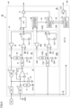
- Fig. 3 is a circuit diagram showing a configuration of ⁇ type A/D converter 92 according to the second embodiment.
- ⁇ type A/D converter 92 in Fig. 3 is different from ⁇ type A/D converter 90 in Fig. 1 in that it further includes a second passive integration circuit 20B and digital circuit 30 further includes a second signal generation circuit 34B and a difference detection circuit 36.
- Second passive integration circuit 20B is an integration circuit similar in configuration to passive integration circuit 20 described with reference to Fig. 1 , the integration circuit being configured with a passive circuit and not including an active element. Second passive integration circuit 20B is configured to temporally integrate a sum of input signal Vin and a digital signal (that is, a feedback voltage V7) outputted from second signal generation circuit 34B of digital circuit 30. In the present disclosure, second passive integration circuit 20B is also referred to as a third integration circuit.
- second passive integration circuit 20B includes resistive elements 21B and 22B and a capacitor 23B.
- Resistive element 22B and capacitor 23B are connected in series in this order between a node 24B on an output side of a buffer element 33B which will be described later and ground GND.
- Resistive element 21B is connected between a node to which input signal Vin is inputted and a connection node 25B between resistive element 22B and capacitor 23B.
- Second signal generation circuit 34B of digital circuit 30 compares an output voltage V6 from second passive integration circuit 20B with threshold voltage Vth at discrete time intervals (specifically, every cycle of clock signal CLK). When output voltage V6 is higher than threshold voltage Vth, second signal generation circuit 34B feeds the digital signal "0" back to second passive integration circuit 20B, and when output voltage V6 is equal to or lower than threshold voltage Vth, second signal generation circuit 34B feeds the digital signal "1" (that is, feedback voltage V7) back to second passive integration circuit 20B. Note that digital circuit 30 may be configured to feed back any of “0” or “1" when output voltage V6 is equal to threshold voltage Vth.
- second signal generation circuit 34B includes a differential input buffer element 31B, a D flip-flop 32B, and buffer element 33B for inverted output.
- Buffer element 31B has a non-inverting input terminal connected to connection node 25B of second passive integration circuit 20B. Threshold voltage Vth is inputted to an inverting input terminal of buffer element 31B.
- An output signal from buffer element 31B is inputted to a D terminal of D flip-flop 32B.
- a digital signal DSB outputted from a Q terminal of D flip-flop 32B is inputted to difference detection circuit 36 and to buffer element 33B.
- Clock signal CLK is inputted to a clock terminal of D flip-flop 32B.
- Buffer element 33B outputs a signal obtained by inversion (feedback voltage V7) of inputted digital signal DSB to one end of resistive element 22B.
- reference voltage Vref When reference voltage Vref is set to be equal to a supply voltage of buffer element 33B, this voltage serves as a reference voltage of a primary ⁇ modulator 91B configured with second passive integration circuit 20B and second signal generation circuit 34B.
- threshold voltage Vth when threshold voltage Vth is set to Vref/2, circuit operations are suitably symmetrical.
- the digital signal "0" is defined as the Low level and the digital signal “1” is defined as the High level.
- a negative feedback circuit necessary for primary ⁇ type modulator 91B can thus be configured without a subtractor, and simplified passive integration circuit 20 can be employed.
- the digital signal "0" fed back from second signal generation circuit 34B of digital circuit 30 may be defined as the High level and the digital signal "1" may be defined as the Low level, second passive integration circuit 20B should perform a subtraction function in that case.
- Difference detection circuit 36 receives digital signal DS outputted from D flip-flop 32 of signal generation circuit 34 and digital signal DSB outputted from D flip-flop 32B of second signal generation circuit 34B. When a difference between a time average of digital signal DS and a time average of digital signal DSB becomes equal to or larger than a certain threshold value, signal generation circuit 34 outputs a fault sensing signal FS.
- digital circuit 30 in Fig. 3 can also be configured with an individual semiconductor element, or with a programmable logic device or a microprocessor.
- an FPGA which is one type of the programmable logic device often includes a differential input buffer, and it is suitable for highly integrated mount of a large number of A/D conversion circuits and other digital circuits.
- Fig. 3 is otherwise similar in configuration to Fig. 1 , the same or corresponding elements have the same reference numerals allotted and description will not be repeated.
- ⁇ type A/D converter 92 in Fig. 3 An operation of ⁇ type A/D converter 92 in Fig. 3 will now be described. Initially, since operations of secondary ⁇ modulator 91 configured with active integration circuit 10, passive integration circuit 20, and signal generation circuit 34 in Fig. 3 are as described above in the first embodiment, detailed description will not be repeated.
- Digital signal DS the ratio of 0/1 of which is varied with analog input signal Vin, is obtained from D flip-flop 32 of signal generation circuit 34.
- D flip-flop 32 when voltage V1 of analog input signal Vin is equal to or lower than 0 V, D flip-flop 32 always outputs 0, and a frequency of output of 1 from D flip-flop 32 becomes higher in proportion to voltage V1 of analog input signal Vin.
- Primary ⁇ modulator 91B is configured with second passive integration circuit 20B and second signal generation circuit 34B in Fig. 3 that are newly added.
- second passive integration circuit 20B a resistance value of resistive element 21B is denoted as Ri3, a resistance value of resistive element 22B is denoted as Rf3, and a capacitance value of capacitor 23B is denoted as Ci3.
- a transfer function of second passive integration circuit 20B is expressed as below. V1 / Ri2 + V7 / Rf2 / s • Ci3
- a sum of a constant multiple of input voltage V1 and a constant multiple of feedback voltage V7 is integrated.
- second passive integration circuit 20B is an RC integration circuit, it can be regarded as an integrator only in a region where variation in output voltage V6 therefrom is less. Therefore, a time constant of Rf3•Ci3 is set to sufficiently be larger than time of delay (that is, the clock cycle) by the delay unit. Variation in voltage in capacitor 23B is thus suppressed and only a passive element implements the integrator.
- a range of input voltage V1 can be set based on a ratio of gain resistances Ri3 and Rf3 in second passive integration circuit 20B.
- reference voltage Vref is equal to the supply voltage of buffer element 33B in the circuit in Fig. 3
- output voltage V7 from buffer element 33B is reference voltage Vref or 0.
- the lower limit value of input voltage V1 is Vth-(Vref-Vth) ⁇ Ri3/Rf3
- the upper limit value of input voltage V1 is Vth ⁇ (1+Ri3/Rf3).
- a range of input to second passive integration circuit 20B can therefore be set in accordance with the range of input to active integration circuit 10 based on the ratio of gain resistances Ri3 and Rf3.
- D flip-flop 32B of second signal generation circuit 34B outputs digital signal DSB, a ratio of 0/1 of which is varied with input signal Vin.
- D flip-flop 32B when the voltage of analog input signal Vin is equal to or lower than Vth-(Vref-Vth) ⁇ Ri3/Rf3, D flip-flop 32B always outputs 0, and a frequency of output of 1 from D flip-flop 32B becomes higher in proportion to the voltage of analog input signal Vin.
- First ⁇ modulator 91 configured with active integration circuit 10, passive integration circuit 20, and signal generation circuit 34 and second ⁇ modulator 91B configured with second passive integration circuit 20B and second signal generation circuit 34B are designed such that time average values of digital signals DS and DSB outputted in response to the same input signal Vin are equal to each other. Therefore, the input ranges thereof are also designed to be equal to each other. Though designs different in input range can also be made, in that case, difference detection circuit 36 corrects one of the time average of digital signal DS outputted from D flip-flop 32 and the time average of digital signal DSB outputted from D flip-flop 32B, with a linear function. The time averages of corrected digital signals DS and DSB in response to the same input signal Vin are thus equal to each other.
- difference detection circuit 36 outputs fault sensing signal FS.
- first ⁇ modulator 91 fails, the difference between the time averages of digital signals DS and DSB becomes equal to or larger than the threshold value and fault sensing signal FS is outputted. Therefore, a control circuit in a subsequent stage can recognize that a result of A/D conversion is not reliable.
- only single analog semiconductor amplifier 17 as an active component of the analog circuit portion can implement secondary ⁇ type A/D converter 92 with the failure sensing function. Therefore, a highly accurate and highly reliable A/D conversion circuit can be provided with low cost with the use of general-purpose components.
- an A/D conversion system 93 including a plurality of ⁇ type A/D converters 92 in the second embodiment will be described.
- A/D conversion system 93 can make switching to another ⁇ type A/D converter.
- A/D conversion system 93 is applied to a digital control device 201 to control a power conversion circuit 60.
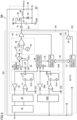
- FIG. 4 is a circuit diagram showing an exemplary configuration of A/D conversion system 93 according to the third embodiment.
- A/D conversion system 93 in the third embodiment includes a plurality of ⁇ type A/D converters similar in configuration to ⁇ type A/D converter 92 in Fig. 3 .
- Each ⁇ type A/D converter receives common input signal Vin.
- a stand-by redundancy system is configured by including a plurality of A/D converters identical in configuration.
- An operating ⁇ type A/D converter will hereinafter be called a main converter.
- A/D conversion system 93 shown in Fig. 4 includes a first ⁇ type A/D converter 94 and a second ⁇ type A/D converter 194 by way of example.
- Digital circuit 30 of first ⁇ type A/D converter 94 further includes a selection circuit 37 and a buffer element 41
- a digital circuit of second ⁇ type A/D converter 194 further includes a selection circuit 137 and a buffer element 141.
- Selection circuit 37 of first ⁇ type A/D converter 94 and selection circuit 137 of second ⁇ type A/D converter 194 are connected to each other through a communication path 50.
- selection circuit 37 is also referred to as a first selection circuit and selection circuit 137 is also referred to as a second selection circuit.
- Selection circuit 37 receives fault sensing signal FS from difference detection circuit 36. While first ⁇ type A/D converter 94 is operating as the main converter, selection circuit 37 of first ⁇ type A/D converter 94 transmits a signal indicating a normal operation to selection circuit 137 of second ⁇ type A/D converter 194. When a power supply is abnormal, when a clock is abnormal, or while selection circuit 37 is receiving fault sensing signal FS from difference detection circuit 36, selection circuit 37 stops transmission of the signal indicating the normal operation. Selection circuit 37 can thus notify selection circuit 137 of a fault of first ⁇ type A/D converter 94.
- Selection circuit 137 of second ⁇ type A/D converter 194 in stand-by monitors a normal operation signal outputted from selection circuit 37 of first ⁇ type A/D converter 94 serving as the main converter.
- Selection circuit 137 performs a function to switch output of the digital signal which is a result of A/D conversion from another converter to the converter to which it belongs, on the occurrence of the fault when the normal operation signal cannot be received.
- selection circuit 37 of currently operating first ⁇ type A/D converter 94 deactivates the output from buffer element 41 and selection circuit 137 of currently stand-by second ⁇ type A/D converter 194 activates the output from buffer element 141.
- Fig. 4 shows an example in which selection circuits 37 and 137 control signals to activate outputs from buffer elements 41 and 141, a switching circuit such as a multiplexer or a selector instead of buffer elements 41 and 141 may be provided.
- a pulsed signal or a serial communication signal rather than a level signal may be used as the normal operation signal outputted from selection circuits 37 and 137.
- the level signal when a circuit element for communication or a communication path fails and a signal is fixed (that is, the signal does not change from a value indicating a normal state), the normal operation and an abnormal state cannot be distinguished from each other.
- the pulsed signal or the serial communication signal when the signal is fixed, a normal signal cannot be received and hence determination as the abnormal state can be made.
- the serial communication signal is used, another type of information can also be superimposed thereon, which is further suitable.
- Fig. 5 is a circuit diagram showing a configuration of digital control device 201 and a digital control power supply 200 including A/D conversion system 93 in Fig. 4 .
- digital control power supply 200 includes power conversion circuit 60 and digital control device 201 to control power conversion circuit 60.
- Digital control device 201 further includes a digital controller 42 in digital circuit 30 of each ⁇ type A/D converter included in A/D conversion system 93 in Fig. 4 .
- Digital controller 42 is a feedback control unit to perform pulse width modulation (PWM) by feedback control based on a result of A/D conversion. Buffer elements 41 and 141 are provided in a stage subsequent to digital controller 42.
- PWM pulse width modulation
- digital controller 42 includes a subtractor 43, a compensator 44, a comparator 45, and a carrier wave oscillator 46. Operations of these constituent elements inclusive of low pass filter 35 will briefly be described below.
- Low pass filter 35 generates a multi-bit digital value Dout from 1-bit digital signal DS subjected to ⁇ modulation.
- Subtractor 43 compares digital value Dout with an output command value OCV to calculate a difference therebetween.
- Compensator 44 calculates a duty as an amount of operation by multiplying the difference calculated by subtractor 43 by an appropriate transfer function.
- Comparator 45 generates a PWM signal by comparing carrier waves generated by carrier wave oscillator 46 with the amount of operation.
- Buffer element 41 outputs a PMW signal generated by comparator 45 to power conversion circuit 60 in a subsequent stage while selection circuit 37 has activated the output.
- Fig. 5 shows a general configuration for PWM by feedback control, a configuration that performs a similar function is available otherwise, and the configuration is not limited to that in Fig. 5 .
- Power conversion circuit 60 controls a voltage and/or a current by ON/OFF control of a power semiconductor element 62.
- a feedback loop is formed by returning an output voltage or an output current from power conversion circuit 60 as input signal Vin to the A/D conversion system.
- a switching regulator digital control power supply 200 to output a desired voltage or current under digital control can be configured.
- Fig. 5 shows a general step-down chopper (that is, a buck converter) circuit by way of example of power conversion circuit 60.
- power conversion circuit 60 in Fig. 5 includes a buffer element 61, power semiconductor element 62, a diode 63, an inductor 64, an input capacitor 65, and an output capacitor 66.
- power semiconductor element 62 and inductor 64 are connected in this order between a power supply node to receive a DC voltage Vdc and an output node to provide output voltage Vout.
- Diode 63 has a cathode connected to a connection node 67 between power semiconductor element 62 and inductor 64 and has a cathode connected to ground GND.
- a PWM signal is inputted to a gate of power semiconductor element 62 through buffer element 61.
- Input capacitor 65 is connected between the power supply node and ground GND.
- Output capacitor 66 is connected between the output node and ground GND.
- Output voltage Vout is fed back to digital control device 201 as input signal Vin.
- Power conversion circuit 60 is not limited to the step-down chopper in Fig. 5 , and any power conversion circuit 60 can be used as being combined with digital control device 201.
- reliability can further be enhanced by constructing redundant A/D conversion system 93 including a plurality of ⁇ type A/D converters 92 in the second embodiment. Furthermore, A/D conversion system 93 in the third embodiment can be applied to digital control device 201 and digital control power supply 200.
- the digital control power supply can be configured by combining digital controller 42 and power conversion circuit 60 in Fig. 5 with ⁇ type A/D converter 90 in the first embodiment.
- the single point of failure refers to an element that causes loss of a function of the entire system by a single failure.
- 10 active integration circuit (first integration circuit); 11 to 14, 21, 21B, 22, 22B, R1 resistive element; 15, 16, 23, 23B, C1 capacitor; 17 analog semiconductor amplifier;
- 20 passive integration circuit (second integration circuit); 20B second passive integration circuit (third integration circuit); 30 digital circuit; 31, 31B differential input buffer element; 33, 33B buffer element for inverted output; 32, 32B D flip-flop; 34 signal generation circuit; 34B second signal generation circuit; 35 low pass filter; 36 difference detection circuit; 37, 137 selection circuit; 42 digital controller (feedback control unit); 43 subtractor; 44 compensator; 45 comparator; 46 carrier wave oscillator; 50 communication path; 60 power conversion circuit; 62 power semiconductor element; 63 diode; 64 inductor; 65 input capacitor; 66 output capacitor; 90, 92 ⁇ type A/D converter; 91 first ⁇ modulator; 91B second ⁇ modulator; 93 A/D conversion system; 94 first ⁇ type A/D converter; 194 second ⁇ type A/D converter; 200 digital control power supply; 201
Landscapes
- Engineering & Computer Science (AREA)
- Theoretical Computer Science (AREA)
- Compression, Expansion, Code Conversion, And Decoders (AREA)
Abstract
Description
- The present disclosure relates to an analog/digital converter, an analog/digital conversion system, a digital control device, and a digital control power supply.
- A technique disclosed, for example, in
Japanese Patent Laying-Open No.2019-057937 - In the ΔΣ type A/D converter described in this literature, a ΔΣ modulation unit includes a first ΔΣ modulation unit an input voltage to which has a voltage value of a voltage to be inspected and a second ΔΣ modulation unit an input voltage to which has a voltage value of a correction reference voltage. A digital filter unit is provided with a first digital filter to generate N-bit data based on information indicated by 1-bit data generated by the first ΔΣ modulation unit and a second digital filter to generate N-bit data based on information indicated by 1-bit data generated by the second ΔΣ modulation unit. A correction computing unit performs correction computation of the N-bit data created by the first digital filter with the N-bit data created by the second digital filter (see the Abstract of PTL 1). In the ΔΣ modulation unit, a resistive element R1 and a capacitor C1 perform a function of a smoothing circuit, a function of a delay DA conversion circuit, and a function of an integration circuit (see paragraphs [0018] and [0019] of PTL 1).
- PTL 1:
Japanese Patent Laying-Open No. 2019-057937 - According to a configuration of the ΔΣ type A/D converter disclosed in
Japanese Patent Laying-Open No. 2019-057937 - The present disclosure was made in view of the background art above, and one of objects thereof is to provide a ΔΣ type A/D converter capable of achieving conversion accuracy higher than in a conventional technique with an inexpensive circuit configuration. Other objects and features of the present disclosure will be described in embodiments below.
- An analog/digital converter in one embodiment includes a first integration circuit, a second integration circuit, and a first signal generation circuit. The first integration circuit temporally integrates a sum of an analog input signal and a first feedback signal and includes an active element. The second integration circuit temporally integrates a sum of a result of integration by the first integration circuit and the first feedback signal and does not include an active element. The first signal generation circuit compares a first output voltage representing a result of integration by the second integration circuit with a threshold voltage at discrete time intervals. The first signal generation circuit generates 1 as a first digital signal when the first output voltage is higher than the threshold voltage and generates 0 as the first digital signal when the first output voltage is lower than the threshold voltage. The first signal generation circuit outputs a signal obtained by inversion of 1 and 0 of the first digital signal as the first feedback signal.
- According to the embodiment above, a secondary ΔΣ type analog/digital converter can be configured with the first integration circuit including the active element and the second integration circuit not including the active element, and hence conversion accuracy can be higher than in the conventional technique with an inexpensive circuit configuration.
-
-
Fig. 1 is a circuit diagram showing a configuration of a ΔΣ type A/D converter 90 according to a first embodiment. -
Fig. 2 is a functional block diagram of asecondary ΔΣ modulator 300 corresponding to ΔΣ type A/D converter 90 inFig. 1 . -
Fig. 3 is a circuit diagram showing a configuration of a ΔΣ type A/D converter 92 according to a second embodiment. -
Fig. 4 is a circuit diagram showing an exemplary configuration of an A/D conversion system 93 according to a third embodiment. -
Fig. 5 is a circuit diagram showing a configuration of adigital control device 201 and a digitalcontrol power supply 200 including A/D conversion system 93 inFig. 4 . - Each embodiment will be described in detail below with reference to the drawings. The same or corresponding elements have the same reference characters allotted and description thereof will not be repeated.
-
Fig. 1 is a circuit diagram showing a configuration of a ΔΣ type A/D converter 90 according to a first embodiment. ΔΣ type A/D converter 90 according to the first embodiment includes an analog circuit portion (10 and 20) and adigital circuit 30. The analog circuit portion (10 and 20) includes anintegration circuit 10 including an active element and anintegration circuit 20 configured with a passive circuit and not including an active element. The active element refers to a semiconductor amplifier and the like configured with an operational amplifier or a discrete component.Integration circuit 10 will also be referred to as anactive integration circuit 10 or afirst integration circuit 10 below andintegration circuit 20 will also be referred to as apassive integration circuit 20 or asecond integration circuit 20 below. A configuration of each ofcircuits 10 to 30 and connection between constituent elements included in each circuit will initially be described. -
Active integration circuit 10 is configured to temporally integrate a sum of an input signal Vin and a digital signal fed back fromdigital circuit 30 toactive integration circuit 10. As shown inFig. 1 ,active integration circuit 10 includesresistive elements 11 to 14,capacitors semiconductor amplifier 17.Semiconductor amplifier 17 is an operational amplifier including a non-inverting input terminal (a + terminal), an inverting input terminal (a - terminal), and an output terminal. -
Resistive element 11 is connected between a node to which input signal Vin is inputted and the non-inverting input terminal ofsemiconductor amplifier 17.Resistive element 12 is connected between anode 24 on an output side of abuffer element 33 which will be described later and the non-inverting input terminal ofsemiconductor amplifier 17.Capacitor 16 is connected between the non-inverting input terminal ofsemiconductor amplifier 17 and a ground GND.Resistive element 13 is connected between the inverting input terminal ofsemiconductor amplifier 17 and ground GND.Resistive element 14 is connected between the inverting input terminal ofsemiconductor amplifier 17 and a node to which a reference voltage Vref is supplied. Capacitor 15 is connected between the inverting input terminal and the output terminal ofsemiconductor amplifier 17. -
Passive integration circuit 20 is configured to temporally integrate a sum of the output signal fromactive integration circuit 10 and a digital signal fed back fromdigital circuit 30 topassive integration circuit 20. As shown inFig. 1 ,passive integration circuit 20 includesresistive elements capacitor 23.Resistive element 22 andcapacitor 23 are connected in series in this order betweennode 24 on the output side ofbuffer element 33 and ground GND.Resistive element 21 is connected between the output terminal ofsemiconductor amplifier 17 ofactive integration circuit 10 and aconnection node 25 betweenresistive element 22 andcapacitor 23. -
Digital circuit 30 compares an output voltage V5 frompassive integration circuit 20 with a threshold voltage Vth at discrete time intervals (specifically, every cycle of a clock signal CLK). When output voltage V5 is higher than threshold voltage Vth,digital circuit 30 feeds a digital signal "0" back toanalog circuit portions digital circuit 30 feeds a digital signal "1" back toanalog circuit portions Digital circuit 30 may be configured to feed "0" or "1" back when output voltage V5 is equal to threshold voltage Vth. As shown inFig. 1 ,digital circuit 30 includes a differentialinput buffer element 31, a D flip-flop 32,buffer element 33 for inverted output, and a low pass filter (LPF) 35. -
Buffer element 31 has a non-inverting input terminal connected toconnection node 25 ofpassive integration circuit 20. Threshold voltage Vth is inputted to an inverting input terminal ofbuffer element 31. An output signal frombuffer element 31 is inputted to a D terminal of D flip-flop 32. A digital signal DS outputted from a Q terminal of D flip-flop 32 is inputted tolow pass filter 35 and tobuffer element 33. Clock signal CLK is inputted to a clock terminal of D flip-flop 32.Buffer element 33 outputs a signal obtained by inversion of 0/1 of inputted digital signal DS to one end ofresistive element 12 and one end ofresistive element 22. - In the present disclosure,
buffer elements flop 32 are collectively referred to as asignal generation circuit 34.Signal generation circuit 34 generates digital signal DS in accordance with input signal Vin and outputs a signal obtained by inversion of 0/1 of digital signal DS as a feedback signal toactive integration circuit 10 andpassive integration circuit 20.Active integration circuit 10,passive integration circuit 20, and signalgeneration circuit 34 implement what is called aΔΣ modulator 91. -
Low pass filter 35 removes quantization noise shifted into a high frequency domain by a noise shaping function ofΔΣ modulator 91. Consequently, a highly accurate digital signal Dout in proportion to analog input signal Vin is outputted from ΔΣ type A/D converter 90. Instead of the low pass filter, processing for counting a ratio of 0 or 1 in digital signal DS outputted fromsignal generation circuit 34 may be performed. -
Digital circuit 30 can also be configured with an individual semiconductor element, or with a programmable logic device or a microprocessor. In particular, a field programmable gate array (FPGA) which is one type of the programmable logic device often includes a differential input buffer, and it is suitable for highly integrated mount of a large number of A/D conversion circuits and other digital circuits. - When reference voltage Vref is set to be equal to a supply voltage of
buffer element 33 inFig. 1 , this voltage serves as the reference voltage of the A/D converter. In addition, when threshold voltage Vth is set to 1/2 of reference voltage Vref, circuit operations are suitably symmetrical. - An operation of ΔΣ type A/
D converter 90 will now be described.Fig. 2 is a functional block diagram of asecondary ΔΣ modulator 300 corresponding to ΔΣ type A/D converter 90 inFig. 1 . - As shown in
Fig. 2 ,ΔΣ modulator 300 includesintegrators adders bit quantizer 331, adelay unit 332, abuffer element 333 for inverted output, and a 1-bit digital-to-analog converter (DAC) 334. In an example wherebuffer element 333 for inverted output is not provided in a stage immediately subsequent to delayunit 332, a subtractor should be provided instead of each ofadders buffer element 333. - An operation in
Fig. 2 will briefly be described.Adder 311 adds a feedback signal V4 to input signal Vin (an input voltage V1).Integrator 310 temporally integrates results of addition byadder 311.Adder 321 adds feedback signal V4 to a voltage V3 representing a result of integration byintegrator 310.Integrator 320 temporally integrates results of addition byadder 321. One-bit quantizer 331 compares voltage V5 representing a result of integration byintegrator 320 with threshold voltage Vth to convert the voltage into a binary digital signal.Delay unit 332 generates digital signal DS by delaying an output from 1-bit quantizer 331 by one clock cycle.Buffer element 333 inverts 0/1 of digital signal DS outputted fromdelay unit 332. Digital/analog converter 334 generates feedback signal V4 by converting the inverted digital signal outputted frombuffer element 333 into an analog signal. - Each functional block in
Fig. 2 is associated with the circuit inFig. 1 as below. Initially,adder 311 andintegrator 310 inFig. 2 correspond toactive integration circuit 10 inFig. 1 .Adder 321 andintegrator 320 inFig. 2 correspond topassive integration circuit 20 inFig. 1 . One-bit quantizer 331 inFig. 2 corresponds to differentialinput buffer element 31 inFig. 1 .Delay unit 332 inFig. 2 corresponds to D flip-flop 32 inFig. 1 .Buffer element 333 and digital/analog converter 334 inFig. 2 correspond to bufferelement 33 inFig. 1 . - The digital signal "0" is defined as a Low level and the digital signal "1" is defined as a High level. A negative feedback circuit necessary for ΔΣ type A/
D converter 90 can thus be configured without a subtractor, and simplifiedpassive integration circuit 20 can be employed forintegrator 320 in a second stage. Though the digital signal "0" fed back fromdigital circuit 30 may be defined as the High level and the digital signal "1" may be defined as the Low level,analog circuit portions - Operations of
active integration circuit 10 andpassive integration circuit 20 inFig. 1 will be described in detail below. Inactive integration circuit 10, resistance values ofresistive elements resistive elements capacitors 
active integration circuit 10 is represented as below, based on a condition of virtual short of the operational amplifier implemented bysemiconductor amplifier 17 and the input current being 0:
active integration circuit 10, the sum of a constant multiple of input voltage V1 and a constant multiple of a feedback voltage V2 is integrated. - When input voltage V1 is in a direct-current (DC) steady state, an output from
active integration circuit 10 has some constant value. In this case, since an input toactive integration circuit 10 is 0 because of differentiation of the output, relation below is satisfied.
- With an expression (3) above, it can be seen that a range of input voltage V1 can be set based on a ratio of gain resistances Ri1 and Rf1 in
active integration circuit 10. For example, when reference voltage Vref is equal to the supply voltage ofbuffer element 33 inFig. 1 , an output voltage V4 frombuffer element 33 is reference voltage Vref or 0. Therefore, voltage V2 expressed in the expression (1) above is 0 or -Vref. By substituting this value of voltage V2 into the expression (3) above, a lower limit value of input voltage V1 is 0 V and an upper limit value of input voltage V1 is Vref×Ri1/Rf1. - Since an offset voltage can be increased or decreased by changing connection of a resistor as in the case of a general differential amplification circuit, the lower limit value of input voltage V1 is not limited to 0 V. For example, a negative voltage can also be inputted as input voltage V1.
- Similarly, in
passive integration circuit 20 inFig. 1 , a resistance value ofresistive element 21 is denoted as Ri2, a resistance value ofresistive element 22 is denoted as Rf2, and a capacitance value ofcapacitor 23 is denoted as Ci2. In this case, a transfer function ofpassive integration circuit 20 is expressed in an expression below:
passive integration circuit 20, a sum of a constant multiple of output voltage V3 fromactive integration circuit 10 and a constant multiple of feedback voltage V4 is integrated. - Since
passive integration circuit 20 is an RC integration circuit, it can be regarded as an integrator only in a region where variation in output voltage V5 therefrom is less. Therefore, a time constant of Rf2•Ci2 is set to sufficiently be larger than time of delay (that is, the clock cycle) bydelay unit 332. Variation in voltage ofcapacitor 23 is thus suppressed and only a passive element implements the integrator. - In the steady state, the output from
passive integration circuit 20 is kept at a constant value (that is, threshold voltage Vth). In this case, since the input topassive integration circuit 20 is 0 because of differentiation of the output, relation below is satisfied.
- With an expression (5) above, it can be seen that a range of input voltage V3 can be set based on a ratio of gain resistances Ri2 and Rf2 in
passive integration circuit 20. For example, when reference voltage Vref is equal to the supply voltage ofbuffer element 33 in the circuit inFig. 1 , output voltage V4 frombuffer element 33 is reference voltage Vref or 0. By substituting this voltage V4 into the expression (4) above, the lower limit value of input voltage V3 is Vth-(Vref-Vth)×Ri2/Rf2 and the upper limit value of input voltage V3 is Vth×(1+Ri2/Rf2). Thus, a range of input topassive integration circuit 20 can be set in accordance with output characteristics ofsemiconductor amplifier 17 included inactive integration circuit 10. - D flip-
flop 32 inFig. 1 outputs digital signal DS, a ratio of 0/1 of which is varied with analog input signal Vin. Specifically, in the circuit configuration inFig. 1 , when voltage V1 of analog input signal Vin is equal to or lower than 0 V, D flip-flop 32 always outputs 0, and a frequency of output of 1 becomes higher in proportion to voltage V1 of analog input signal Vin. - As set forth above, according to the first embodiment, only a single analog semiconductor amplifier as an active component of the analog circuit portion can implement secondary ΔΣ type A/
D converter 90. Therefore, a highly accurate A/D conversion circuit can be provided with low cost with the use of general-purpose components. - In a second embodiment, a ΔΣ type A/
D converter 92 enhanced in reliability by addition of a failure sensing function to ΔΣ type A/D converter 90 in the first embodiment will be described. -
Fig. 3 is a circuit diagram showing a configuration of ΔΣ type A/D converter 92 according to the second embodiment. ΔΣ type A/D converter 92 inFig. 3 is different from ΔΣ type A/D converter 90 inFig. 1 in that it further includes a secondpassive integration circuit 20B anddigital circuit 30 further includes a secondsignal generation circuit 34B and adifference detection circuit 36. - Second
passive integration circuit 20B is an integration circuit similar in configuration topassive integration circuit 20 described with reference toFig. 1 , the integration circuit being configured with a passive circuit and not including an active element. Secondpassive integration circuit 20B is configured to temporally integrate a sum of input signal Vin and a digital signal (that is, a feedback voltage V7) outputted from secondsignal generation circuit 34B ofdigital circuit 30. In the present disclosure, secondpassive integration circuit 20B is also referred to as a third integration circuit. - More specifically, second
passive integration circuit 20B includesresistive elements capacitor 23B.Resistive element 22B andcapacitor 23B are connected in series in this order between anode 24B on an output side of abuffer element 33B which will be described later and ground GND.Resistive element 21B is connected between a node to which input signal Vin is inputted and aconnection node 25B betweenresistive element 22B andcapacitor 23B. - Second
signal generation circuit 34B ofdigital circuit 30 compares an output voltage V6 from secondpassive integration circuit 20B with threshold voltage Vth at discrete time intervals (specifically, every cycle of clock signal CLK). When output voltage V6 is higher than threshold voltage Vth, secondsignal generation circuit 34B feeds the digital signal "0" back to secondpassive integration circuit 20B, and when output voltage V6 is equal to or lower than threshold voltage Vth, secondsignal generation circuit 34B feeds the digital signal "1" (that is, feedback voltage V7) back to secondpassive integration circuit 20B. Note thatdigital circuit 30 may be configured to feed back any of "0" or "1" when output voltage V6 is equal to threshold voltage Vth. - More specifically, similarly to signal
generation circuit 34 described with reference toFig. 1 , secondsignal generation circuit 34B includes a differentialinput buffer element 31B, a D flip-flop 32B, andbuffer element 33B for inverted output.Buffer element 31B has a non-inverting input terminal connected toconnection node 25B of secondpassive integration circuit 20B. Threshold voltage Vth is inputted to an inverting input terminal ofbuffer element 31B. An output signal frombuffer element 31B is inputted to a D terminal of D flip-flop 32B. A digital signal DSB outputted from a Q terminal of D flip-flop 32B is inputted todifference detection circuit 36 and to bufferelement 33B. Clock signal CLK is inputted to a clock terminal of D flip-flop 32B.Buffer element 33B outputs a signal obtained by inversion (feedback voltage V7) of inputted digital signal DSB to one end ofresistive element 22B. - When reference voltage Vref is set to be equal to a supply voltage of
buffer element 33B, this voltage serves as a reference voltage of aprimary ΔΣ modulator 91B configured with secondpassive integration circuit 20B and secondsignal generation circuit 34B. In addition, when threshold voltage Vth is set to Vref/2, circuit operations are suitably symmetrical. - The digital signal "0" is defined as the Low level and the digital signal "1" is defined as the High level. A negative feedback circuit necessary for primary
ΔΣ type modulator 91B can thus be configured without a subtractor, and simplifiedpassive integration circuit 20 can be employed. Though the digital signal "0" fed back from secondsignal generation circuit 34B ofdigital circuit 30 may be defined as the High level and the digital signal "1" may be defined as the Low level, secondpassive integration circuit 20B should perform a subtraction function in that case. -
Difference detection circuit 36 receives digital signal DS outputted from D flip-flop 32 ofsignal generation circuit 34 and digital signal DSB outputted from D flip-flop 32B of secondsignal generation circuit 34B. When a difference between a time average of digital signal DS and a time average of digital signal DSB becomes equal to or larger than a certain threshold value,signal generation circuit 34 outputs a fault sensing signal FS. - As in the first embodiment,
digital circuit 30 inFig. 3 can also be configured with an individual semiconductor element, or with a programmable logic device or a microprocessor. In particular, an FPGA which is one type of the programmable logic device often includes a differential input buffer, and it is suitable for highly integrated mount of a large number of A/D conversion circuits and other digital circuits. - Since
Fig. 3 is otherwise similar in configuration toFig. 1 , the same or corresponding elements have the same reference numerals allotted and description will not be repeated. - An operation of ΔΣ type A/
D converter 92 inFig. 3 will now be described. Initially, since operations ofsecondary ΔΣ modulator 91 configured withactive integration circuit 10,passive integration circuit 20, and signalgeneration circuit 34 inFig. 3 are as described above in the first embodiment, detailed description will not be repeated. Digital signal DS, the ratio of 0/1 of which is varied with analog input signal Vin, is obtained from D flip-flop 32 ofsignal generation circuit 34. Specifically, in the circuit configuration inFig. 3 , when voltage V1 of analog input signal Vin is equal to or lower than 0 V, D flip-flop 32 always outputs 0, and a frequency of output of 1 from D flip-flop 32 becomes higher in proportion to voltage V1 of analog input signal Vin. -
Primary ΔΣ modulator 91B is configured with secondpassive integration circuit 20B and secondsignal generation circuit 34B inFig. 3 that are newly added. In secondpassive integration circuit 20B, a resistance value ofresistive element 21B is denoted as Ri3, a resistance value ofresistive element 22B is denoted as Rf3, and a capacitance value ofcapacitor 23B is denoted as Ci3. In this case, a transfer function of secondpassive integration circuit 20B is expressed as below.
passive integration circuit 20B, a sum of a constant multiple of input voltage V1 and a constant multiple of feedback voltage V7 is integrated. - Since second
passive integration circuit 20B is an RC integration circuit, it can be regarded as an integrator only in a region where variation in output voltage V6 therefrom is less. Therefore, a time constant of Rf3•Ci3 is set to sufficiently be larger than time of delay (that is, the clock cycle) by the delay unit. Variation in voltage incapacitor 23B is thus suppressed and only a passive element implements the integrator. - In the steady state, the output from second
passive integration circuit 20B is kept at a constant value (that is, threshold voltage Vth). In this case, since the input to secondpassive integration circuit 20B is 0 because of differentiation of the output, relation below is satisfied.
- With an expression (7) above, it can be seen that a range of input voltage V1 can be set based on a ratio of gain resistances Ri3 and Rf3 in second
passive integration circuit 20B. For example, when reference voltage Vref is equal to the supply voltage ofbuffer element 33B in the circuit inFig. 3 , output voltage V7 frombuffer element 33B is reference voltage Vref or 0. By substituting this voltage V7 into the expression (7) above, the lower limit value of input voltage V1 is Vth-(Vref-Vth)×Ri3/Rf3 and the upper limit value of input voltage V1 is Vth×(1+Ri3/Rf3). A range of input to secondpassive integration circuit 20B can therefore be set in accordance with the range of input toactive integration circuit 10 based on the ratio of gain resistances Ri3 and Rf3. - D flip-
flop 32B of secondsignal generation circuit 34B outputs digital signal DSB, a ratio of 0/1 of which is varied with input signal Vin. Specifically, in the circuit configuration inFig. 3 , when the voltage of analog input signal Vin is equal to or lower than Vth-(Vref-Vth)×Ri3/Rf3, D flip-flop 32B always outputs 0, and a frequency of output of 1 from D flip-flop 32B becomes higher in proportion to the voltage of analog input signal Vin. -
First ΔΣ modulator 91 configured withactive integration circuit 10,passive integration circuit 20, and signalgeneration circuit 34 andsecond ΔΣ modulator 91B configured with secondpassive integration circuit 20B and secondsignal generation circuit 34B are designed such that time average values of digital signals DS and DSB outputted in response to the same input signal Vin are equal to each other. Therefore, the input ranges thereof are also designed to be equal to each other. Though designs different in input range can also be made, in that case,difference detection circuit 36 corrects one of the time average of digital signal DS outputted from D flip-flop 32 and the time average of digital signal DSB outputted from D flip-flop 32B, with a linear function. The time averages of corrected digital signals DS and DSB in response to the same input signal Vin are thus equal to each other. - As described previously, when the difference between the time average of digital signal DS outputted from D flip-
flop 32 and the time average of digital signal DSB outputted from D flip-flop 32B becomes equal to or larger than a certain threshold value,difference detection circuit 36 outputs fault sensing signal FS. Thus, whenfirst ΔΣ modulator 91 fails, the difference between the time averages of digital signals DS and DSB becomes equal to or larger than the threshold value and fault sensing signal FS is outputted. Therefore, a control circuit in a subsequent stage can recognize that a result of A/D conversion is not reliable. - As set forth above, according to the second embodiment, only single
analog semiconductor amplifier 17 as an active component of the analog circuit portion can implement secondary ΔΣ type A/D converter 92 with the failure sensing function. Therefore, a highly accurate and highly reliable A/D conversion circuit can be provided with low cost with the use of general-purpose components. - In a third embodiment, an A/
D conversion system 93 including a plurality of ΔΣ type A/D converters 92 in the second embodiment will be described. When an operating ΔΣ type A/D converter fails, A/D conversion system 93 can make switching to another ΔΣ type A/D converter. Furthermore, an example in which A/D conversion system 93 is applied to adigital control device 201 to control apower conversion circuit 60 will be described. -
Fig. 4 is a circuit diagram showing an exemplary configuration of A/D conversion system 93 according to the third embodiment. A/D conversion system 93 in the third embodiment includes a plurality of ΔΣ type A/D converters similar in configuration to ΔΣ type A/D converter 92 inFig. 3 . Each ΔΣ type A/D converter receives common input signal Vin. A stand-by redundancy system is configured by including a plurality of A/D converters identical in configuration. An operating ΔΣ type A/D converter will hereinafter be called a main converter. - A/
D conversion system 93 shown inFig. 4 includes a first ΔΣ type A/D converter 94 and a second ΔΣ type A/D converter 194 by way of example.Digital circuit 30 of first ΔΣ type A/D converter 94 further includes aselection circuit 37 and abuffer element 41, and a digital circuit of second ΔΣ type A/D converter 194 further includes aselection circuit 137 and abuffer element 141.Selection circuit 37 of first ΔΣ type A/D converter 94 andselection circuit 137 of second ΔΣ type A/D converter 194 are connected to each other through acommunication path 50. In the present disclosure,selection circuit 37 is also referred to as a first selection circuit andselection circuit 137 is also referred to as a second selection circuit. -
Selection circuit 37 receives fault sensing signal FS fromdifference detection circuit 36. While first ΔΣ type A/D converter 94 is operating as the main converter,selection circuit 37 of first ΔΣ type A/D converter 94 transmits a signal indicating a normal operation toselection circuit 137 of second ΔΣ type A/D converter 194. When a power supply is abnormal, when a clock is abnormal, or whileselection circuit 37 is receiving fault sensing signal FS fromdifference detection circuit 36,selection circuit 37 stops transmission of the signal indicating the normal operation.Selection circuit 37 can thus notifyselection circuit 137 of a fault of first ΔΣ type A/D converter 94. -
Selection circuit 137 of second ΔΣ type A/D converter 194 in stand-by monitors a normal operation signal outputted fromselection circuit 37 of first ΔΣ type A/D converter 94 serving as the main converter.Selection circuit 137 performs a function to switch output of the digital signal which is a result of A/D conversion from another converter to the converter to which it belongs, on the occurrence of the fault when the normal operation signal cannot be received. InFig. 4 ,selection circuit 37 of currently operating first ΔΣ type A/D converter 94 deactivates the output frombuffer element 41 andselection circuit 137 of currently stand-by second ΔΣ type A/D converter 194 activates the output frombuffer element 141. ThoughFig. 4 shows an example in whichselection circuits buffer elements buffer elements - A pulsed signal or a serial communication signal rather than a level signal may be used as the normal operation signal outputted from
selection circuits -
Fig. 5 is a circuit diagram showing a configuration ofdigital control device 201 and a digitalcontrol power supply 200 including A/D conversion system 93 inFig. 4 . - Referring to
Fig. 5 , digitalcontrol power supply 200 includespower conversion circuit 60 anddigital control device 201 to controlpower conversion circuit 60.Digital control device 201 further includes adigital controller 42 indigital circuit 30 of each ΔΣ type A/D converter included in A/D conversion system 93 inFig. 4 .Digital controller 42 is a feedback control unit to perform pulse width modulation (PWM) by feedback control based on a result of A/D conversion.Buffer elements digital controller 42. - Specifically, in the example shown in
Fig. 5 ,digital controller 42 includes asubtractor 43, acompensator 44, acomparator 45, and acarrier wave oscillator 46. Operations of these constituent elements inclusive oflow pass filter 35 will briefly be described below. -
Low pass filter 35 generates a multi-bit digital value Dout from 1-bit digital signal DS subjected to ΔΣ modulation.Subtractor 43 compares digital value Dout with an output command value OCV to calculate a difference therebetween.Compensator 44 calculates a duty as an amount of operation by multiplying the difference calculated bysubtractor 43 by an appropriate transfer function.Comparator 45 generates a PWM signal by comparing carrier waves generated bycarrier wave oscillator 46 with the amount of operation.Buffer element 41 outputs a PMW signal generated bycomparator 45 topower conversion circuit 60 in a subsequent stage whileselection circuit 37 has activated the output. - Though
Fig. 5 shows a general configuration for PWM by feedback control, a configuration that performs a similar function is available otherwise, and the configuration is not limited to that inFig. 5 . -
Power conversion circuit 60 controls a voltage and/or a current by ON/OFF control of apower semiconductor element 62. A feedback loop is formed by returning an output voltage or an output current frompower conversion circuit 60 as input signal Vin to the A/D conversion system. Thus, a switching regulator (digital control power supply 200) to output a desired voltage or current under digital control can be configured. -
Fig. 5 shows a general step-down chopper (that is, a buck converter) circuit by way of example ofpower conversion circuit 60. Specifically,power conversion circuit 60 inFig. 5 includes abuffer element 61,power semiconductor element 62, adiode 63, aninductor 64, aninput capacitor 65, and anoutput capacitor 66. - As shown in
Fig. 5 ,power semiconductor element 62 andinductor 64 are connected in this order between a power supply node to receive a DC voltage Vdc and an output node to provide output voltage Vout.Diode 63 has a cathode connected to aconnection node 67 betweenpower semiconductor element 62 andinductor 64 and has a cathode connected to ground GND. A PWM signal is inputted to a gate ofpower semiconductor element 62 throughbuffer element 61.Input capacitor 65 is connected between the power supply node and ground GND.Output capacitor 66 is connected between the output node and ground GND. Output voltage Vout is fed back todigital control device 201 as input signal Vin. -
Power conversion circuit 60 is not limited to the step-down chopper inFig. 5 , and anypower conversion circuit 60 can be used as being combined withdigital control device 201. - As set forth above, according to the third embodiment, reliability can further be enhanced by constructing redundant A/
D conversion system 93 including a plurality of ΔΣ type A/D converters 92 in the second embodiment. Furthermore, A/D conversion system 93 in the third embodiment can be applied todigital control device 201 and digitalcontrol power supply 200. - The configurations in the first to third embodiments are by way of example and are not limited, and the configurations incorporating existing known techniques can freely be combined for use. For example, the digital control power supply can be configured by combining
digital controller 42 andpower conversion circuit 60 inFig. 5 with ΔΣ type A/D converter 90 in the first embodiment. - In configuring a highly reliable system, there is a concept of a single point of failure. The single point of failure refers to an element that causes loss of a function of the entire system by a single failure. By adopting ΔΣ type A/
D converter 92 in the second embodiment or A/D conversion system 93 in the third embodiment in a signal path where a single point of failure may occur and adopting ΔΣ type A/D converter 90 in the first embodiment in a signal path where a single point of failure may not occur, a system for which resistance to failure is ensured as a whole can be realized at minimum cost. - It should be understood that the embodiments disclosed herein are illustrative and non-restrictive in every respect. The scope of this application is defined by the terms of the claims rather than the description above and is intended to include any modifications within the scope and meaning equivalent to the terms of the claims.
- 10 active integration circuit (first integration circuit); 11 to 14, 21, 21B, 22, 22B, R1 resistive element; 15, 16, 23, 23B, C1 capacitor; 17 analog semiconductor amplifier; 20 passive integration circuit (second integration circuit); 20B second passive integration circuit (third integration circuit); 30 digital circuit; 31, 31B differential input buffer element; 33, 33B buffer element for inverted output; 32, 32B D flip-flop; 34 signal generation circuit; 34B second signal generation circuit; 35 low pass filter; 36 difference detection circuit; 37, 137 selection circuit; 42 digital controller (feedback control unit); 43 subtractor; 44 compensator; 45 comparator; 46 carrier wave oscillator; 50 communication path; 60 power conversion circuit; 62 power semiconductor element; 63 diode; 64 inductor; 65 input capacitor; 66 output capacitor; 90, 92 ΔΣ type A/D converter; 91 first ΔΣ modulator; 91B second ΔΣ modulator; 93 A/D conversion system; 94 first ΔΣ type A/D converter; 194 second ΔΣ type A/D converter; 200 digital control power supply; 201 digital control device; 300 ΔΣ modulator; 310, 320 integrator; 311, 321 adder; 331 1-bit quantizer; 332 delay unit; 333 output inverting buffer element; 334 digital/analog converter; CLK clock signal; DS, DSB, Dout digital signal; FS fault sensing signal; GND ground; OCV output command value; V2, V4, V7 feedback voltage; V3, V6 output voltage; Vref reference voltage; Vth threshold voltage.
Claims (7)
- An analog/digital converter comprising:a first integration circuit to temporally integrate a sum of an analog input signal and a first feedback signal, the first integration circuit comprising an active element;a second integration circuit to temporally integrate a sum of a result of integration by the first integration circuit and the first feedback signal, the second integration circuit not comprising an active element; anda first signal generation circuit to compare a first output voltage representing a result of integration by the second integration circuit with a threshold voltage at discrete time intervals, the first signal generation circuit generating 1 as a first digital signal when the first output voltage is higher than the threshold voltage and generating 0 as the first digital signal when the first output voltage is lower than the threshold voltage, the first signal generation circuit outputting a signal obtained by inversion of 1 and 0 of the first digital signal as the first feedback signal.
- The analog/digital converter according to claim 1, further comprising:a third integration circuit to temporally integrate a sum of the analog input signal and a second feedback signal, the third integration circuit not comprising an active element;a second signal generation circuit to compare a second output voltage representing a result of integration by the third integration circuit with the threshold voltage at discrete time intervals, the second signal generation circuit generating 1 as a second digital signal when the second output voltage is higher than the threshold voltage and generating 0 as the second digital signal when the second output voltage is lower than the threshold voltage, the second signal generation circuit outputting a signal obtained by inversion of 1 and 0 of the second digital signal as the second feedback signal; anda difference detection circuit to output a fault sensing signal when a difference between a time average of the first digital signal and a time average of the second digital signal is equal to or larger than a threshold value.
- An analog/digital conversion system comprising:a first converter and a second converter each configured as the analog/digital converter according to claim 2;a first selection circuit to select whether to output the first digital signal to outside, the first digital signal being a result of A/D conversion of the analog input signal by the first converter; anda second selection circuit to select whether to output the first digital signal to the outside, the first digital signal being a result of A/D conversion of the analog input signal by the second converter, whereinwhen the fault sensing signal is outputted from the difference detection circuit of the first converter while the first digital signal is being outputted from the first converter to the outside, the first selection circuit stops output of the first digital signal from the first converter and notifies the second selection circuit that the first digital signal is to be outputted from the second converter.
- An analog/digital conversion system comprising:a first converter configured as the analog/digital converter according to claim 2; anda second converter comprising the first integration circuit, the second integration circuit, and the first signal generation circuit and not comprising the third integration circuit, the second signal generation circuit, and the difference detection circuit, whereinthe first converter is provided in a signal path where a single point of failure may occur, andthe second converter is provided in a signal path where a single point of failure may not occur.
- The analog/digital converter according to claim 2, wherein
at least a part of a digital circuit comprising the first signal generation circuit, the second signal generation circuit, and the difference detection circuit is implemented by a programmable logic device or a microprocessor. - A digital control device comprising:the analog/digital converter according to claim 2; anda feedback control unit to generate an operation signal based on a difference between the first digital signal and an output command value.
- A digital control power supply comprising:the digital control device according to claim 6; anda power conversion circuit comprising a semiconductor switching element controlled in accordance with the operation signal, whereina voltage or a current outputted from the power conversion circuit is used as the analog input signal.
Applications Claiming Priority (1)
| Application Number | Priority Date | Filing Date | Title |
|---|---|---|---|
| PCT/JP2022/009122 WO2023166659A1 (en) | 2022-03-03 | 2022-03-03 | Analog-to-digital converter, analog-to-digital conversion system, digital control device, and digital control power source |
Publications (2)
| Publication Number | Publication Date |
|---|---|
| EP4489308A1 true EP4489308A1 (en) | 2025-01-08 |
| EP4489308A4 EP4489308A4 (en) | 2025-04-09 |
Family
ID=87883299
Family Applications (1)
| Application Number | Title | Priority Date | Filing Date |
|---|---|---|---|
| EP22929804.7A Pending EP4489308A4 (en) | 2022-03-03 | 2022-03-03 | Analog-to-digital converter, analog-to-digital conversion system, digital control device, and digital control power source |
Country Status (4)
| Country | Link |
|---|---|
| US (1) | US20250192795A1 (en) |
| EP (1) | EP4489308A4 (en) |
| JP (1) | JP7668953B2 (en) |
| WO (1) | WO2023166659A1 (en) |
Family Cites Families (10)
| Publication number | Priority date | Publication date | Assignee | Title |
|---|---|---|---|---|
| JPS63248222A (en) * | 1987-04-03 | 1988-10-14 | Nippon Telegr & Teleph Corp <Ntt> | Delta sigma type a/d converter |
| JP3012887B2 (en) * | 1989-03-13 | 2000-02-28 | 日本テキサス・インスツルメンツ株式会社 | Signal converter |
| US5068657A (en) * | 1990-05-25 | 1991-11-26 | At&T Bell Laboratories | Method and apparatus for testing delta-sigma modulators |
| US5471209A (en) * | 1994-03-03 | 1995-11-28 | Echelon Corporation | Sigma-delta converter having a digital logic gate core |
| JP3776752B2 (en) * | 2001-06-07 | 2006-05-17 | 新電元工業株式会社 | DC-DC converter |
| US6930624B2 (en) * | 2003-10-31 | 2005-08-16 | Texas Instruments Incorporated | Continuous time fourth order delta sigma analog-to-digital converter |
| US8462030B2 (en) * | 2004-04-27 | 2013-06-11 | Texas Instruments Incorporated | Programmable loop filter for use with a sigma delta analog-to-digital converter and method of programming the same |
| US9654133B2 (en) * | 2014-12-17 | 2017-05-16 | Analog Devices, Inc. | Microprocessor-assisted calibration for analog-to-digital converter |
| US9509332B1 (en) * | 2015-11-06 | 2016-11-29 | Freescale Semiconductor, Inc. | Dual sigma-delta analog-to-digital converter |
| JP2019057937A (en) | 2018-12-06 | 2019-04-11 | ダイヤモンド電機株式会社 | Delta-sigma ad conversion processing device |
-
2022
- 2022-03-03 JP JP2024504129A patent/JP7668953B2/en active Active
- 2022-03-03 US US18/842,483 patent/US20250192795A1/en active Pending
- 2022-03-03 EP EP22929804.7A patent/EP4489308A4/en active Pending
- 2022-03-03 WO PCT/JP2022/009122 patent/WO2023166659A1/en not_active Ceased
Also Published As
| Publication number | Publication date |
|---|---|
| JPWO2023166659A1 (en) | 2023-09-07 |
| WO2023166659A1 (en) | 2023-09-07 |
| EP4489308A4 (en) | 2025-04-09 |
| US20250192795A1 (en) | 2025-06-12 |
| JP7668953B2 (en) | 2025-04-25 |
Similar Documents
| Publication | Publication Date | Title |
|---|---|---|
| US10008994B2 (en) | Audio amplifier system | |
| EP1965496B1 (en) | Delta-sigma type ad converter, class-d amplifier, and dc-dc coverter | |
| US9077243B2 (en) | Current-balancing in interleaved circuit phases using a parameter common to the phases | |
| US7489119B2 (en) | DC to DC converter with reference voltage loop disturbance compensation | |
| US7365668B2 (en) | Continuous-time delta-sigma analog digital converter having operational amplifiers | |
| US10763887B2 (en) | Sigma delta analog to digital converter | |
| US11009563B2 (en) | Signal processing arrangement for a hall sensor and signal processing method for a hall sensor | |
| CN108696281B (en) | Power scaling continuous time delta sigma modulator | |
| US20070075886A1 (en) | Transmitting and receiving device and transmitting device and receiving device | |
| EP4489308A1 (en) | Analog-to-digital converter, analog-to-digital conversion system, digital control device, and digital control power source | |
| US12113443B2 (en) | Multi-converter power supply system | |
| US12101029B2 (en) | Multi-converter power supply system | |
| US7408494B2 (en) | Continuous-time delta-sigma analog digital converter | |
| EP4050803B1 (en) | Tracking analog-to-digital converter for power converters | |
| JPWO2013140914A1 (en) | Transmitter and transmission method | |
| US20250298062A1 (en) | Voltage detection circuit | |
| EP4701086A1 (en) | Adc circuit with dac including capacitance | |
| US20250321252A1 (en) | Voltage detection circuit | |
| US11245414B2 (en) | Delta-sigma modulator and method of driving delta-sigma modulator | |
| US20260005684A1 (en) | Current synthesizer | |
| JP7006214B2 (en) | Signal generator and signal generation method | |
| US20070103945A1 (en) | Starting circuit and method for the stable starting of a circuit arrangement with plural feedback control circuits | |
| JPH02170723A (en) | A/d converting circuit | |
| JPWO2023166659A5 (en) | ||
| CN121939979A (en) | Analog frequency locking circuit, method and power converter applying same |
Legal Events
| Date | Code | Title | Description |
|---|---|---|---|
| STAA | Information on the status of an ep patent application or granted ep patent |
Free format text: STATUS: THE INTERNATIONAL PUBLICATION HAS BEEN MADE |
|
| PUAI | Public reference made under article 153(3) epc to a published international application that has entered the european phase |
Free format text: ORIGINAL CODE: 0009012 |
|
| STAA | Information on the status of an ep patent application or granted ep patent |
Free format text: STATUS: REQUEST FOR EXAMINATION WAS MADE |
|
| 17P | Request for examination filed |
Effective date: 20240809 |
|
| AK | Designated contracting states |
Kind code of ref document: A1 Designated state(s): AL AT BE BG CH CY CZ DE DK EE ES FI FR GB GR HR HU IE IS IT LI LT LU LV MC MK MT NL NO PL PT RO RS SE SI SK SM TR |
|
| REG | Reference to a national code |
Ref country code: DE Ref legal event code: R079 Free format text: PREVIOUS MAIN CLASS: H03M0001080000 Ipc: H03M0003020000 |
|
| A4 | Supplementary search report drawn up and despatched |
Effective date: 20250312 |
|
| RIC1 | Information provided on ipc code assigned before grant |
Ipc: H03M 3/02 20060101AFI20250306BHEP |
|
| DAV | Request for validation of the european patent (deleted) | ||
| DAX | Request for extension of the european patent (deleted) |