EP4489301A1 - Amplificateur de puissance doherty multi-bandes - Google Patents
Amplificateur de puissance doherty multi-bandes Download PDFInfo
- Publication number
- EP4489301A1 EP4489301A1 EP24187200.1A EP24187200A EP4489301A1 EP 4489301 A1 EP4489301 A1 EP 4489301A1 EP 24187200 A EP24187200 A EP 24187200A EP 4489301 A1 EP4489301 A1 EP 4489301A1
- Authority
- EP
- European Patent Office
- Prior art keywords
- amplifier
- amplification path
- band
- band amplification
- stage
- Prior art date
- Legal status (The legal status is an assumption and is not a legal conclusion. Google has not performed a legal analysis and makes no representation as to the accuracy of the status listed.)
- Pending
Links
Images



Classifications
-
- H—ELECTRICITY
- H03—ELECTRONIC CIRCUITRY
- H03F—AMPLIFIERS
- H03F1/00—Details of amplifiers with only discharge tubes, only semiconductor devices or only unspecified devices as amplifying elements
- H03F1/02—Modifications of amplifiers to raise the efficiency, e.g. gliding Class A stages, use of an auxiliary oscillation
- H03F1/0205—Modifications of amplifiers to raise the efficiency, e.g. gliding Class A stages, use of an auxiliary oscillation in transistor amplifiers
- H03F1/0288—Modifications of amplifiers to raise the efficiency, e.g. gliding Class A stages, use of an auxiliary oscillation in transistor amplifiers using a main and one or several auxiliary peaking amplifiers whereby the load is connected to the main amplifier using an impedance inverter, e.g. Doherty amplifiers
-
- H—ELECTRICITY
- H03—ELECTRONIC CIRCUITRY
- H03F—AMPLIFIERS
- H03F1/00—Details of amplifiers with only discharge tubes, only semiconductor devices or only unspecified devices as amplifying elements
- H03F1/08—Modifications of amplifiers to reduce detrimental influences of internal impedances of amplifying elements
- H03F1/22—Modifications of amplifiers to reduce detrimental influences of internal impedances of amplifying elements by use of cascode coupling, i.e. earthed cathode or emitter stage followed by earthed grid or base stage respectively
- H03F1/223—Modifications of amplifiers to reduce detrimental influences of internal impedances of amplifying elements by use of cascode coupling, i.e. earthed cathode or emitter stage followed by earthed grid or base stage respectively with MOSFET's
-
- H—ELECTRICITY
- H03—ELECTRONIC CIRCUITRY
- H03F—AMPLIFIERS
- H03F1/00—Details of amplifiers with only discharge tubes, only semiconductor devices or only unspecified devices as amplifying elements
- H03F1/56—Modifications of input or output impedances, not otherwise provided for
-
- H—ELECTRICITY
- H03—ELECTRONIC CIRCUITRY
- H03F—AMPLIFIERS
- H03F1/00—Details of amplifiers with only discharge tubes, only semiconductor devices or only unspecified devices as amplifying elements
- H03F1/56—Modifications of input or output impedances, not otherwise provided for
- H03F1/565—Modifications of input or output impedances, not otherwise provided for using inductive elements
-
- H—ELECTRICITY
- H03—ELECTRONIC CIRCUITRY
- H03F—AMPLIFIERS
- H03F3/00—Amplifiers with only discharge tubes or only semiconductor devices as amplifying elements
- H03F3/189—High-frequency amplifiers, e.g. radio frequency amplifiers
- H03F3/19—High-frequency amplifiers, e.g. radio frequency amplifiers with semiconductor devices only
- H03F3/195—High-frequency amplifiers, e.g. radio frequency amplifiers with semiconductor devices only in integrated circuits
-
- H—ELECTRICITY
- H03—ELECTRONIC CIRCUITRY
- H03F—AMPLIFIERS
- H03F3/00—Amplifiers with only discharge tubes or only semiconductor devices as amplifying elements
- H03F3/20—Power amplifiers, e.g. Class B amplifiers, Class C amplifiers
- H03F3/21—Power amplifiers, e.g. Class B amplifiers, Class C amplifiers with semiconductor devices only
- H03F3/211—Power amplifiers, e.g. Class B amplifiers, Class C amplifiers with semiconductor devices only using a combination of several amplifiers
-
- H—ELECTRICITY
- H03—ELECTRONIC CIRCUITRY
- H03F—AMPLIFIERS
- H03F3/00—Amplifiers with only discharge tubes or only semiconductor devices as amplifying elements
- H03F3/20—Power amplifiers, e.g. Class B amplifiers, Class C amplifiers
- H03F3/24—Power amplifiers, e.g. Class B amplifiers, Class C amplifiers of transmitter output stages
- H03F3/245—Power amplifiers, e.g. Class B amplifiers, Class C amplifiers of transmitter output stages with semiconductor devices only
-
- H—ELECTRICITY
- H03—ELECTRONIC CIRCUITRY
- H03F—AMPLIFIERS
- H03F3/00—Amplifiers with only discharge tubes or only semiconductor devices as amplifying elements
- H03F3/72—Gated amplifiers, i.e. amplifiers which are rendered operative or inoperative by means of a control signal
-
- H—ELECTRICITY
- H03—ELECTRONIC CIRCUITRY
- H03F—AMPLIFIERS
- H03F2200/00—Indexing scheme relating to amplifiers
- H03F2200/111—Indexing scheme relating to amplifiers the amplifier being a dual or triple band amplifier, e.g. 900 and 1800 MHz, e.g. switched or not switched, simultaneously or not
-
- H—ELECTRICITY
- H03—ELECTRONIC CIRCUITRY
- H03F—AMPLIFIERS
- H03F2200/00—Indexing scheme relating to amplifiers
- H03F2200/141—Indexing scheme relating to amplifiers the feedback circuit of the amplifier stage comprising a resistor and a capacitor in series, at least one of them being an active one
-
- H—ELECTRICITY
- H03—ELECTRONIC CIRCUITRY
- H03F—AMPLIFIERS
- H03F2200/00—Indexing scheme relating to amplifiers
- H03F2200/213—A variable capacitor being added in the input circuit, e.g. base, gate, of an amplifier stage
-
- H—ELECTRICITY
- H03—ELECTRONIC CIRCUITRY
- H03F—AMPLIFIERS
- H03F2200/00—Indexing scheme relating to amplifiers
- H03F2200/222—A circuit being added at the input of an amplifier to adapt the input impedance of the amplifier
-
- H—ELECTRICITY
- H03—ELECTRONIC CIRCUITRY
- H03F—AMPLIFIERS
- H03F2200/00—Indexing scheme relating to amplifiers
- H03F2200/318—A matching circuit being used as coupling element between two amplifying stages
-
- H—ELECTRICITY
- H03—ELECTRONIC CIRCUITRY
- H03F—AMPLIFIERS
- H03F2200/00—Indexing scheme relating to amplifiers
- H03F2200/387—A circuit being added at the output of an amplifier to adapt the output impedance of the amplifier
-
- H—ELECTRICITY
- H03—ELECTRONIC CIRCUITRY
- H03F—AMPLIFIERS
- H03F2200/00—Indexing scheme relating to amplifiers
- H03F2200/39—Different band amplifiers are coupled in parallel to broadband the whole amplifying circuit
-
- H—ELECTRICITY
- H03—ELECTRONIC CIRCUITRY
- H03F—AMPLIFIERS
- H03F2200/00—Indexing scheme relating to amplifiers
- H03F2200/423—Amplifier output adaptation especially for transmission line coupling purposes, e.g. impedance adaptation
-
- H—ELECTRICITY
- H03—ELECTRONIC CIRCUITRY
- H03F—AMPLIFIERS
- H03F2200/00—Indexing scheme relating to amplifiers
- H03F2200/429—Two or more amplifiers or one amplifier with filters for different frequency bands are coupled in parallel at the input or output
-
- H—ELECTRICITY
- H03—ELECTRONIC CIRCUITRY
- H03F—AMPLIFIERS
- H03F2200/00—Indexing scheme relating to amplifiers
- H03F2200/451—Indexing scheme relating to amplifiers the amplifier being a radio frequency amplifier
-
- H—ELECTRICITY
- H03—ELECTRONIC CIRCUITRY
- H03F—AMPLIFIERS
- H03F2200/00—Indexing scheme relating to amplifiers
- H03F2200/61—Indexing scheme relating to amplifiers the cascode amplifier has more than one common gate stage
-
- H—ELECTRICITY
- H03—ELECTRONIC CIRCUITRY
- H03F—AMPLIFIERS
- H03F2203/00—Indexing scheme relating to amplifiers with only discharge tubes or only semiconductor devices as amplifying elements covered by H03F3/00
- H03F2203/72—Indexing scheme relating to gated amplifiers, i.e. amplifiers which are rendered operative or inoperative by means of a control signal
- H03F2203/7209—Indexing scheme relating to gated amplifiers, i.e. amplifiers which are rendered operative or inoperative by means of a control signal the gated amplifier being switched from a first band to a second band
Definitions
- the present invention relates to a multi-band Doherty power amplifier.
- the invention is particularly applicable to telecommunications equipment usable in mobile telephone networks or in WiFi networks.
- Modern communication standards such as 4G/5G/6G and WiFi6/6E/7 significantly increase the complexity of RF front-end modules, of which the power amplifier represents a critical part, in terms of size and power consumption.
- the signals used in the 4G/5G/6G and Wifi6/6E/7 standards have high peak-to-average power ratios (PAPR) (greater than 4 dB), due in particular to the presence of a large number of modulated subcarriers in these OFDM-type communication systems.
- PAPR peak-to-average power ratios
- power back-off is a power level below the saturation point that allows the amplifier to operate in a linear region.
- power amplifiers operate near the saturation point because this is where efficiency is at its highest.
- the level of power reduction is called "Power Back-off”.
- the power amplifier In state-of-the-art power amplifiers, power backoff significantly degrades the average efficiency of the power amplifier. Thus, in addition to the power amplifier having to maintain high efficiency despite power backoff, the power amplifier must also be broadband or multi-band in order to support an increased number of frequency bands.
- the Doherty power amplifier represents an interesting solution for efficient amplification of high PAPR signals.
- the operating principle of the Doherty amplifier is illustrated by the figure 1 , and in more detail in [1].
- the RF input signal IN is pre-amplified by a pre-amplification stage 1, and the signal is separated by a power divider 5.
- the Doherty amplifier comprises a main amplifier 2, an auxiliary amplifier 3, an impedance matching circuit 6 at the input of the main amplifier 2 and the auxiliary amplifier 3, and an output impedance matching circuit 4 comprising a quarter-wave line here acting as an impedance inverter. It is possible to consider other types of combiners which do not necessarily use a quarter-wave line.
- the impedance matching circuit 6 applies a predetermined phase compensation between the main chain and the auxiliary chain.
- An output matching network (not shown) can optionally transform the load impedance of the system (typically 50 Ohm) into an optimal operating impedance.
- the Doherty power amplifier uses the concept of active (or dynamic) load modulation, in which the load seen by the main amplifier 2 is modulated by injecting a current from the auxiliary amplifier 3.
- the main amplifier 2, typically operating in class AB, is always active, while the auxiliary amplifier 3, typically operating in class C or deep AB, contributes only in the backoff region.
- Doherty power amplifiers typically have a limited optimum operating bandwidth (fractional band FBW ⁇ 10%) and require precise phase control at the impedance matching circuit 6 to maintain high performance (efficiency and linearity) over the target frequency band.
- FBW Fmax ⁇ Fmin / Fcentral
- Fmin the minimum frequency of the operating band
- Fmax the maximum frequency of the operating band
- Fcentral the center frequency
- a Doherty power amplifier architecture with a wide frequency band (1.55 - 2.3 GHz) includes several tunable capacitors.
- the amplifier requires the use of a digital (external) pre-distortion technique, in order to maintain the required level of linearity over the entire frequency band, which is detrimental to the energy efficiency of the system.
- an alternative Doherty power amplifier architecture has linear behavior over the 1.9 GHz - 2.7 GHz band without requiring any digital pre-distortion technique.
- the amplifier includes tunable capacitors integrated on SOI-CMOS, which improves the frequency linearity.
- the FBW operating bandwidth remains below 25%.
- An object of the invention is therefore a Doherty amplifier as defined in claims 1 to 5.
- the Doherty amplifier according to the invention is illustrated by the Figures 2a , 2b And 2c .
- the PE input port receives the RF signal from RF IN to be amplified.
- a PRA pre-amplification stage is used to amplify the RF signal from RF IN , so as to generate an intermediate signal SI, to increase the overall gain of the Doherty amplifier.
- a common network RCO which includes a switch SW, is connected at the output of the pre-amplification stage PRA.
- the common network RCO is also connected to a high-band amplification path VA HB and to a low-band amplification path VA LB.
- the switch SW can selectively activate the high-band amplification path VA HB or the low-band amplification path VA LB depending on the carrier frequency of the input RF signal.
- the Doherty amplifier also includes external means for adjusting the bias signals for the transistors depending on whether the high-band amplification path VA HB or the low-band amplification path VA LB is selected.
- the switch SW comprises an input terminal BE, connected to the pre-amplification stage PRA, and two output terminals.
- An output terminal BS1 is connected to the high-band amplification channel VA HB
- an output terminal BS2 is connected to the low-band amplification channel VA LB .
- An example of a usable switch is a SPDT (for "Single Pole Double Throw") type switch with one input and two outputs.
- the selection of one or other of the amplification channels of the Doherty amplifier is carried out automatically based on knowledge of the carrier frequency of the signal to be amplified.
- switching between the amplification paths can be performed dynamically, i.e. while the Doherty amplifier is in use.
- the Doherty amplifier integrated in telecommunications equipment (e.g. a base station or a terminal user), can control switching between amplification channels based on user movement and/or user cell change.
- Switching from one amplification channel to another can be controlled by a control device (not shown in the figures).
- the high-band amplification channel VA HB is adapted to amplify the intermediate signal whose operating frequency band is in a so-called higher frequency band.
- the high-band amplification channel VA HB comprises a main amplifier AP HB operating in class AB, and an auxiliary amplifier AA HB operating in class C or deep AB.
- the high-band amplification channel VA HB comprises an output impedance matching network OMN HB connected to the main amplifier AP HB , to the auxiliary amplifier AA HB , and to the output port PS1 at which the amplified signal is taken. The recombination of the signals from the main and auxiliary amplifiers takes place at node A.
- the main/auxiliary amplifier can be made of a transistor (LDMOS type transistor on the Figures 2a And 2b but another type of transistor can be used), a stack of transistors (case of driver stages, but this could also be the case for the output stage), or a combination of transistors.
- the main amplifier and the auxiliary amplifier of each channel comprise LDMOS ("laterally-diffused metal-oxide semiconductor") type transistors, which offer a high breakdown voltage (greater than 10 Volts), which is necessary for applications requiring high output powers (> 1W) such as mobile phones or telecommunications base stations.
- LDMOS laterally-diffused metal-oxide semiconductor
- Other technologies can be considered for the transistors of the power stage, in particular stacked transistors of the MOS+MOS or MOS+LDMOS type, BiCMOS transistors or even GaAs, GaN or InP.
- the output of the main amplifier AP HB is connected to the output of the auxiliary amplifier AA HB (transistor drain) via a lumped-element pi-network impedance inverter equivalent to a quarter-wave line.
- the impedance inverter is composed of a capacitor C invm1 connected between the output of the main amplifier AP HB and ground, of a capacitor C inva1 connected between the output of the auxiliary amplifier AA HB and ground, and of a coil L inv1 connecting the two outputs of the main amplifier AP HB and of the auxiliary amplifier AA HB .
- the output combiner may adopt a different topology, such as a topology described in [4].
- the OMN HB output network comprises a coil L SUPM1 connected between the external supply voltage source V dd of the main amplifier AP HB and the output of the main amplifier AP HB. Similarly, a coil L SUPA1 is connected between the external supply voltage source V dd2 of the auxiliary amplifier AA HB and node A.
- a tunable resonant network consisting of a coil L H2o1 and a variable capacitor C H2o1 , is connected between node A and ground.
- This resonant network constitutes a tunable harmonic termination which is used to improve the rejection of the second harmonic with respect to the fundamental frequency.
- the LC filter composed of a coil L SO1 , a capacitor C SO1 , the capacitor C po1 and the coil L po1 , is part of the output matching network at the fundamental frequency.
- the low-band amplification channel VA LB is suitable for amplifying the intermediate signal whose operating frequency band is in a so-called lower frequency band. It comprises an output impedance matching network of the low-band amplification channel OMN LB which may be identical (but not necessarily) to the output impedance matching network of the high-band amplification channel OMN HB , the dimensioning of the components possibly being different from one channel to another.
- the Doherty amplifier includes a PS1 output port for the VA HB high-band amplifier path and a PS2 output port for the VA HB high-band amplifier path. low band VA LB .
- the PS1 output port of the high band VA HB amplifier channel can be connected to an antenna or an antenna selection switch, and the PS2 output port of the low band VA LB amplifier channel can be connected to a different antenna or an antenna selection switch.
- the upper frequency band and the lower frequency band are preferably disjoint.
- the components of the high band VA HB amplifier path may be sized to amplify the input signal in the 2.1-2.7 GHz operating band
- the components of the low band VA LB amplifier path may be sized to amplify the input signal in the 1.7-2.1 GHz operating band.
- the Doherty amplifier according to the invention comprises an intermediate impedance matching network ISMN2, connected between the pre-amplification stage PRA and each of the main amplifiers (AP HB , AP LB ) and auxiliary amplifiers (AA HB , AA LB ).
- the intermediate impedance matching network ISMN2 makes it possible to present an optimal source impedance to each of the amplifiers. It is advantageously distributed between the common network RCO, the high-band amplification path VA HB and the low-band amplification path VA LB .
- intermediate impedance matching network ISMN2 some of the components of the intermediate impedance matching network ISMN2 are part of the common network RCO, while other components of the intermediate impedance matching network ISMN2 are part of the high-band amplification path VA HB and the low-band amplification path VA LB .
- the design of the ISMN2 intermediate impedance matching network is a critical aspect in order to obtain good RF performance for the Doherty amplifier. Indeed, it must present both an optimal source impedance for the output stages and an optimal load impedance for the pre-amplification stage.
- the power divider stage which allows the signal power to be distributed between the main amplifier AP HB and the auxiliary amplifier AA HB , comprises a first resonant circuit LC1 arranged in the common network RCO, a second resonant circuit RC2 arranged in the high band amplification path VA HB , and a third resonant circuit RC3 arranged in the low band amplification path VA LB.
- the first resonant circuit LC1 includes a capacitor C CD connected between the output of the pre-amplification stage PRA and the input terminal of the switch SW, and an inductor L div connected between the input terminal of the switch SW and ground.
- the second resonant circuit RC2 comprises two capacitors (C div11 , C div12 ) connected in parallel through the resistor R div1 . Both capacitors are connected to the output terminal of the switch SW which activates the high-band amplification path VA HB .
- the capacitor C div11 is on the main amplifier branch AP HB
- the capacitor C div12 is on the auxiliary amplifier branch AA HB .
- An inductance L pa1 is connected between the capacitor C div12 and ground.
- the resistor R div1 connects the capacitors (C div11 , C div12 ) connected in parallel.
- the resistor R div1 can be a variable resistor, in order to adjust the amplitude and phase on the high-band amplification path VA HB .
- the shared inductance L div thus forms a modified Wilkinson divider with the capacitors C div11 and C div12 and the resistor R div1 when the high band amplification channel VA HB is activated and with the capacitors C div21 and C div22 , and the resistor R div2 when the low band amplification channel VA LB is activated.
- the third resonant circuit RC3 consists of two capacitors (C div21 , C div22 ) connected in parallel through the resistor R div2 .
- the two capacitors are connected to the output terminal of the switch SW which activates the low-band amplification path VA LB .
- the resistor R div2 connects the capacitors (C div21 , C div22 ) connected in parallel.
- a first tunable resonant network RRA1 HB is connected to the gate of the main amplifier AP HB and configured to introduce a first predefined phase shift ⁇ m .
- the first tunable resonant network RRA1 HB comprises an inductance L pm1 , connected between the second resonant circuit RC2 and ground, and a variable capacitor C sm1 connected between the second resonant circuit RLC2 and the gate of the main amplifier AP HB .
- a second tunable resonant network RRA2 HB is connected to the gate of the auxiliary amplifier AA HB and configured to introduce a second predefined phase shift ⁇ a .
- the second tunable resonant network RRA2 LB comprises an inductance L pa1 , connected between a node B1 and ground.
- Node B1 connects the second resonant circuit RC2 to the gate of the auxiliary amplifier AA HB via a variable capacitor C sa1 placed in series with an inductance L sa1 .
- a capacitor C pa1 is connected between an intermediate point located between the variable capacitor C sa1 and the inductance L sa1 , and ground.
- the first tunable resonant network RRA1 HB is sized and adjusted so that it presents the optimum source impedance to the main amplifier AP HB while introducing the first predefined phase shift ⁇ m .
- the second tunable resonant network RRA2 HB is sized and adjusted so that it presents the optimum source impedance to the auxiliary amplifier AP LB while introducing the second predefined phase shift ⁇ a .
- a first tunable resonant network RRA1 LB is identical to the first resonant network RRA1 HB of the high-band amplification path VA HB .
- the first tunable resonant network RRA1 LB introduces a first predefined phase shift ⁇ m .
- a second tunable resonant network RRA2 LB is connected to the gate of the auxiliary amplifier AA LB and configured to introduce a second predefined phase shift ⁇ a to the RF signal.
- the second tunable resonant network RRA2 LB comprises a variable capacitor C sa2 connected in series with an inductance L sa2 .
- a capacitor C pa2 is connected between an intermediate point located between the variable capacitor C sa2 and the inductance L sa2 , and ground.
- the second tunable resonant network RRA2 LB of the low-band amplification channel VA LB does not comprise an inductance connected between the node B2 and the ground.
- the second tunable resonant network RRA2 LB of the low-band amplification channel VA LB thus comprises one less inductance (or coil) than the second tunable resonant network RRA2 HB of the high-band amplification channel VA HB .
- the SW switch does not provide perfect isolation between the high-band amplification path VA HB and the low-band amplification path VA LB .
- the intermediate impedance matching network ISMN2 is able to form the required impedance and phase level taking into account the parasitics of the inactive path (i.e. the high-band amplification path VA HB ).
- the variable capacitors of the amplification paths and the bias voltages of the transistors can also be adjusted so that the performances are optimized according to the target frequency.
- the resistor R div2 of the third resonant circuit RC3 can be a variable resistor, which allows to adjust the required amplitude and phase levels taking into account the parasitics of the inactive path.
- the parasitic impedance of the high-band amplification path VA HB makes it possible to do without an additional bulky inductance in the second tunable resonant network RRA2 LB of the low-band amplification path VA LB.
- the value of the first phase shift ⁇ m and the value of the second phase shift ⁇ a are determined so that their difference has a predefined value in the back-off region of the main amplifier (AP HB , AP LB ) and the auxiliary amplifier (AA HB , AA LB ).
- the difference ⁇ diff depends on the power due to the non-linearity of the input impedances of the main amplifier and the auxiliary amplifier. These input impedances, as well as the transfer function of the intermediate impedance matching networks, vary with frequency. These effects induce a variation of ⁇ diff and degrade the performance of the Doherty amplifier. To avoid such degradation, ⁇ diff is optimized and readjusted in the back-off zone (typical back-off value of 4 to 8 dB for mobile applications).
- the baseband impedances at the gate and drain of the main amplifier and the auxiliary amplifier introduce a memory effect and cause a degradation of the linearity performance.
- the main amplifier and the auxiliary amplifier are biased via a parallel LC resonator (L tank11 -C tank11 , L tank12 -C tank12 , L tank21 -C tank21 , L tank22 -C tank22 ,) connected to the gate of the transistors.
- the pre-amplification stage PRA (or "driver" according to the English terminology) comprises two stages connected in cascade, with a first amplifier stage DRV1 and a second amplifier stage DRV2 (connected to an external power source via an inductance L supd ), in order to maintain a high power gain (typically of the order of 30 dB) for all operating frequencies in high and low bands (a power gain of 30 dB or more can be obtained with two pre-amplification stages, compared to less than 30 dB with a single pre-amplification stage).
- a high power gain typically of the order of 30 dB
- the power gain can be reduced, due to the intrinsic gain characteristics of the transistors (for a given output power and therefore a given transistor size).
- the second amplifier DRV2 is connected directly to the intermediate impedance matching network ISMN2, in particular to the capacitor C CD of the common network RCO.
- the first amplifier DRV1 and/or the second amplifier DRV2 advantageously comprise a common gate transistor (T11, T12) and a common source transistor (T21, T22), according to a cascode type assembly. This topology makes it possible to maximize the overall gain of the Doherty amplifier.
- a MOS transistor for example of the body-contact BC-MOS type in SOI technology
- an LDMOS transistor can be used for the common gate transistor (T11 and T12).
- This embodiment is however not exclusive, and it can be envisaged to use the LDMOS transistor for all the transistors of the PRA pre-amplification stage.
- the PRA pre-amplification stage also includes an input impedance matching network IMN configured to adapt the input impedance of the first stage DRV1 to a predefined source impedance value (typically 50 Ohm).
- a capacitor C10 connected to the input port PE, is connected to the gate of the common source T21 via a capacitor C15.
- An inductance L11 is connected between an intermediate point located between the two capacitors, and ground.
- the gate of the common source T21 is biased via a resistor R14.
- the common gate T11 is biased via a resistor R12.
- a capacitor C13 is connected between resistor R12 and ground.
- the pre-amplification stage PRA comprises a second impedance matching network ISMN1 connected between the first stage DRV1 and the second stage DRV2 (inductances L16 and L p2 , resistor R19, and capacitors C17 and C18, connected similarly to the components of the input impedance matching network IMN).
- the second impedance matching network ISMN1 may comprise a second harmonic filter PSH, connected between the grid of the common source T22 and ground.
- the second harmonic filter PSH comprises an inductor L H2i in series with a capacitor C H2i , which may be adjustable in order to control the second harmonic impedance with respect to the carrier frequency.
- a feedback circuit CRE comprising a capacitor C21 and a variable resistor R20 in series is connected between the drain of the common gate transistor T11 and the gate of the common source transistor T21.
- the adjustment of the value of the variable resistor R20 is carried out according to the selected amplification channel.
- each of the variable capacitors used in the Doherty amplifier is composed of a fixed-value capacitor, a set of coarse-tuning capacitors, and a set of fine-tuning capacitors, connected in parallel.
- the set of coarse-tuning capacitors and the set of fine-tuning capacitors are composed of multiple branches of variable capacitors, each capacitor being connected to a stack of transistors in order to weight the value of the coarse tuning or the fine tuning.
- the quality factor (Q) of the variable capacitor defines the TR adjustment range (ratio between maximum and minimum capacitance value), and the voltage value across the capacitor determines the number of stacked transistors (N) as well as the gate width of the transistors (Wg). Several transistors are stacked to support the maximum voltage level in the OFF state.
- variable capacitors There are other ways to realize variable capacitors depending on the integration technology considered (RF-MEMS or BST technologies for example)
- FIG. 3 illustrates the simulated performance of the Doherty amplifier according to the invention, for different operating frequencies.
- the left column represents the input-output transmission parameter S21 (power gain, in dB) and input adaptation S11 as a function of the operating frequency.
- the middle column represents the power added efficiency PAE (for "Power Added Efficiency"), in percent, as a function of the output power P out (in dBm).
- the right column represents the AM/AM (amplitude modulation to amplitude modulation) and AM/PM (amplitude modulation to phase modulation) linearity characteristics.
- the Doherty amplifier maintains high efficiency, and according to the AM/AM and AM/PM characteristic curves, very good linearity is achieved over the 1.7-2.7 GHz frequency range.
- ACLR for “Adjacent Channel Leakage power Ratio” is defined as the ratio of the average filtered power centered on the assigned channel frequency to the average filtered power centered on an adjacent channel frequency.
- the added power efficiency PAE allows to characterize energy efficiency well, while the filtered average power ratio ACLR allows to characterize linearity well in the presence of an amplitude and phase modulated transmission signal.
- the following table also illustrates the very good efficiency and linearity performances of the Doherty amplifier according to the invention (ACLR measured for the LTE wireless communication standard, E-UTRA for “Evolved Universal Terrestrial Radio Access”): Setting Low band High Band Unit Freq. 1.7 1.8 2.0 2.3 2.5 2.7 GHz Pout 28 dBm PAE 40 42.1 42.8 42.8 42.7 41.2 % ACLR -37.7 -36.6 -34.8 -35.7 -38 -33.8 dBc FOM 77.7 78.7 77.6 78.5 80.6 75
- the Doherty amplifier makes it possible to obtain a FOM figure of merit greater than 75 over the entire 1.7-2.7 GHz band by providing an output power P out equal to 28 dBm, without using digital predistortion.
Landscapes
- Engineering & Computer Science (AREA)
- Power Engineering (AREA)
- Microelectronics & Electronic Packaging (AREA)
- Amplifiers (AREA)
Abstract
L'invention se rapporte à un amplificateur Doherty comprenant :- un port d'entrée ;- un étage de pré-amplification ;- au moins un port de sortie ;caractérisé en ce que l'amplificateur Doherty comprend en outre :- une voie d'amplification bande haute ;- une voie d'amplification bande basse ;la voie d'amplification bande haute (VA<sub>HB</sub>) et la voie d'amplification bande basse comprenant chacune un amplificateur principal, un amplificateur auxiliaire, et un réseau d'adaptation d'impédance de sortie ;- un réseau commun connecté à la voie d'amplification bande haute et à la voie d'amplification bande basse, le réseau commun comprenant un commutateur configuré pour activer sélectivement la voie d'amplification bande haute ou la voie d'amplification bande basse ;dans lequel un réseau intermédiaire d'adaptation d'impédance est réparti entre le réseau commun, la voie d'amplification bande haute et la voie d'amplification bande basse.
Description
- La présente invention se rapporte à un amplificateur de puissance Doherty multi-bandes. L'invention est applicable en particulier aux équipements de télécommunications utilisables dans les réseaux de téléphonie mobile ou dans les réseaux WiFi.
- Les standards de communication modernes du type 4G/5G/6G et WiFi6/6E/7 augmentent considérablement la complexité des modules frontaux RF, dont l'amplificateur de puissance représente une partie critique, en termes de taille et de consommation d'énergie.
- En effet, le besoin d'une consommation d'énergie réduite avec une taille et un coût de fabrication réduits, pousse la recherche vers des amplificateurs de puissance multi-bandes à haut rendement et à haut niveau d'intégration, avec de fortes exigences de linéarité.
- Les signaux utilisés dans les standards 4G/5G/6G et Wifi6/6E/7 ont des rapports de puissance crête à puissance moyenne (PAPR pour « Peak-to-Average Power Ratio ») élevés (supérieur à 4 dB), en raison, notamment, de la présence d'un grand nombre de sous-porteuses modulées dans ces systèmes de communication de type OFDM.
- Avec un PAPR élevé, il est d'autant plus nécessaire d'abaisser le niveau de puissance de l'amplificateur de puissance par rapport à la puissance crête (« back-off » selon la terminologie anglo-saxonne), afin de répondre à des spécifications de linéarité strictes.
- Plus précisément, le « back-off » de puissance est un niveau de puissance inférieur au point de saturation qui permet de faire fonctionner l'amplificateur dans une zone linéaire. Habituellement, les amplificateurs de puissance fonctionnent près du point de saturation car c'est là que l'efficacité est maximale. Pour s'assurer que l'amplificateur fonctionne dans la zone linéaire, le niveau de puissance est abaissé à partir du point d'efficacité maximale. Le niveau de réduction de puissance est appelé « Power Back-off » (ou « back-off » de puissance).
- Dans les amplificateurs de puissance de l'état de l'art, la réduction de puissance dégrade considérablement l'efficacité moyenne de l'amplificateur de puissance. Ainsi, outre le fait que l'amplificateur de puissance doive conserver une efficacité élevée malgré le back-off de puissance, l'amplificateur de puissance doit également être à large bande ou multi-bandes afin de prendre en charge un nombre accru de bandes de fréquences.
- L'amplificateur de puissance Doherty représente une solution intéressante pour une amplification efficace des signaux à PAPR élevés. Le principe de fonctionnement de l'amplificateur Doherty est illustré par la
figure 1 , et plus en détails dans [1]. Le signal d'entrée RFIN est pré-amplifié par un étage de pré-amplification 1, et le signal est séparé par un diviseur de puissance 5. L'amplificateur Doherty comprend un amplificateur principal 2, un amplificateur auxiliaire 3, un circuit d'adaptation d'impédance 6 en entrée de l'amplificateur principal 2 et de l'amplificateur auxiliaire 3, et un circuit d'adaptation d'impédance en sortie 4 comprenant une ligne quart d'onde jouant ici le rôle d'inverseur d'impédance. Il est possible de considérer d'autres types de combineurs qui n'utilisent pas forcément de ligne quart d'onde. Le circuit d'adaptation d'impédance 6 applique une compensation de phase prédéterminée entre la chaîne principale et la chaîne auxiliaire. Un réseau d'adaptation en sortie (non représenté) permet éventuellement de transformer l'impédance de charge du système (classiquement 50 Ohm) en une impédance optimale de fonctionnement. - L'amplificateur de puissance Doherty utilise le concept de modulation de charge active (ou dynamique), dans lequel la charge vue par l'amplificateur principal 2 est modulée en injectant un courant à partir de l'amplificateur auxiliaire 3. L'amplificateur principal 2, fonctionnant classiquement en classe AB, est toujours actif, tandis que l'amplificateur auxiliaire 3, fonctionnant classiquement en classe C ou AB profonde, ne contribue que dans la région de backoff.
- Les amplificateurs de puissance Doherty ont généralement une bande de fonctionnement optimale limitée (bande fractionnaire FBW < 10%) et nécessitent un contrôle de phase précis au niveau du circuit d'adaptation d'impédance 6 pour maintenir des performances (efficacité et linéarité) élevées sur la bande de fréquence visée.
- La bande fractionnaire de fonctionnement est donnée par la relation suivante :

- Avec Fmin la fréquence minimum de la bande de fonctionnement, Fmax la fréquence maximum de la bande de fonctionnement, et Fcentral la fréquence centrale.
- Pour surmonter la dégradation des performances des amplificateurs de puissance Doherty sur une gamme de fréquences élevée, des architectures d'amplificateurs de puissance Doherty accordables ont été récemment introduites.
- Dans [2], une architecture d'amplificateur de puissance Doherty ayant une bande de fréquences élargie (1,55 - 2,3 GHz) comprend plusieurs condensateurs accordables. L'amplificateur nécessite l'utilisation d'une technique de pré-distorsion numérique (externe), afin de maintenir le niveau de linéarité requis sur toute la bande de fréquence, ce qui nuit à l'efficacité énergétique du système.
- Dans [3], une architecture alternative d'amplificateur de puissance Doherty a un comportement linéaire sur la bande 1,9 GHz - 2,7 GHz sans nécessiter de technique de pré-distorsion numérique. L'amplificateur comprend des condensateurs accordables intégrés sur SOI-CMOS, ce qui améliore la linéarité en fréquence. Cependant, la bande de fonctionnement FBW reste inférieure à 25 %.
- Il existe donc un besoin pour fournir un amplificateur de puissance Doherty linéaire ayant une bande de fonctionnement fractionnaire FBW améliorée, et n'utilisant pas de technique de pré-distorsion numérique.
- Un objet de l'invention est donc un amplificateur Doherty tel que défini selon les revendications 1 à 5.
- D'autres caractéristiques, détails et avantages de l'invention ressortiront à la lecture de la description faite en référence aux dessins annexés donnés à titre d'exemple.
- La
figure 1 , déjà décrite, illustre le principe de fonctionnement d'un amplificateur de puissance Doherty. - La
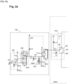
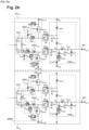
figure 2a et lafigure 2b illustrent des vues en détail d'un circuit d'amplificateur de puissance Doherty selon l'invention, et lafigure 2c illustre une variante de lafigure 2b . - La
figure 3 illustre différentes performances obtenues avec le circuit d'amplificateur de puissance Doherty selon l'invention. - L'amplificateur Doherty selon l'invention est illustré par les
figures 2a ,2b et2c . - Le port d'entrée PE reçoit le signal RF d'entrée RFIN à amplifier. Un étage de de pré-amplification PRA permet d'amplifier le signal RF d'entrée RFIN, de façon à générer un signal intermédiaire SI, pour augmenter le gain global de l'amplificateur Doherty.
- Un réseau commun RCO, qui comprend un commutateur SW, est connecté en sortie de l'étage de pré-amplification PRA. Le réseau commun RCO est également connecté à une voie d'amplification bande haute VAHB et à une voie d'amplification bande basse VALB. Le commutateur SW peut activer sélectivement la voie d'amplification bande haute VAHB ou la voie d'amplification bande basse VALB en fonction de la fréquence porteuse du signal RF d'entrée. L'amplificateur Doherty comprend également des moyens externes de réglage des signaux de polarisation pour les transistors selon que la voie d'amplification bande haute VAHB ou la voie d'amplification bande basse VALB soit sélectionnée.
- A cet effet, le commutateur SW comprend une borne d'entrée BE, connectée à l'étage de pré-amplification PRA, et deux bornes de sortie. Une borne de sortie BS1 est connectée à la voie d'amplification bande haute VAHB, et une borne de sortie BS2 est connectée à la voie d'amplification bande basse VALB. Un exemple de commutateur utilisable est un interrupteur de type SPDT (pour « Single Pole Double Throw ») à une entrée et deux sortie.
- La sélection de l'une ou l'autre des voies d'amplification de l'amplificateur Doherty est effectuée automatiquement en fonction de la connaissance de la fréquence porteuse du signal à amplifier.
- Par exemple, la commutation entre les voies d'amplification peut être effectuée de façon dynamique, c'est-à-dire en cours d'utilisation de l'amplificateur Doherty. Selon un autre mode de réalisation, l'amplificateur Doherty, intégré dans un équipement de télécommunications (par exemple une station de base ou un terminal utilisateur), peut commander la commutation entre les voies d'amplification en fonction du déplacement de l'utilisateur et/ou du changement de cellule de l'utilisateur.
- La commutation d'une voie d'amplification à l'autre peut être commandée par un dispositif de commande (non représenté sur les figures).
- La voie d'amplification bande haute VAHB est adaptée pour amplifier le signal intermédiaire dont la bande de fréquence de fonctionnement se trouve dans une bande de fréquences dite supérieure. Selon le principe de fonctionnement de l'amplificateur Doherty rappelé précédemment, la voie d'amplification bande haute VAHB comprend un amplificateur principal APHB fonctionnant en classe AB, et un amplificateur auxiliaire AAHB fonctionnant en classe C ou AB profonde. Par ailleurs, la voie d'amplification bande haute VAHB comprend un réseau d'adaptation d'impédance de sortie OMNHB connecté à l'amplificateur principal APHB, à l'amplificateur auxiliaire AAHB, et au port de sortie PS1 au niveau duquel le signal amplifié est prélevé. La recombinaison des signaux issus des amplificateurs principal et auxiliaire a lieu au niveau du noeud A.
- L'amplificateur principal/auxiliaire peut être constitué d'un transistor (transistor de type LDMOS sur les
figures 2a et2b mais un autre type de transistor peut être utilisé), d'un empilement de transistors (cas des étages de drivers, mais cela pourrait également être le cas pour l'étage de sortie), ou d'une combinaison de transistors. - De façon avantageuse, l'amplificateur principal et l'amplificateur auxiliaire de chaque voie comprennent des transistors de type LDMOS (« laterally-diffused metal-oxide semiconductor »), qui offrent une tension de claquage élevée (supérieure à 10 Volts), ce qui est nécessaire pour des applications nécessitant de fortes puissances de sortie (> 1W) telles que les téléphones mobiles ou les stations de base de télécommunications. D'autres technologies peuvent être envisagées pour les transistors de l'étage de puissance, notamment des transistors empilés de type MOS+MOS ou MOS+LDMOS, des transistors BiCMOS ou encore GaAs, GaN ou InP.
- Selon un mode de réalisation, la sortie de l'amplificateur principal APHB (drain du transistor) est connectée à la sortie de l'amplificateur auxiliaire AAHB (drain du transistor) par le biais d'un inverseur d'impédance de type réseau en pi à éléments localisés équivalent à une ligne quart d'onde. L'inverseur d'impédance est composé d'un condensateur Cinvm1 connecté entre la sortie de l'amplificateur principal APHB et la masse, d'un condensateur Cinva1 connecté entre la sortie de l'amplificateur auxiliaire AAHB et la masse, et d'une bobine Linv1 reliant les deux sorties de l'amplificateur principal APHB et de l'amplificateur auxiliaire AAHB.
- Le combineur de sortie peut adopter une topologie différente, telle qu'une topologie décrite dans [4].
- Les condensateurs Cinvm1 et Cinva1, et la bobine Linv1 sont dimensionnés de façon à ce que l'impédance caractéristique Zc de l'inverseur d'impédance soit égale à Zc = 2 × Zopt, avec Zopt l'impédance de charge optimale au noeud A qui correspond à la sortie de l'amplificateur auxiliaire AAHB.
- Le réseau de sortie OMNHB comprend une bobine LSUPM1 connectée entre la source de tension d'alimentation externe Vdd de l'amplificateur principal APHB et la sortie de l'amplificateur principal APHB De même, une bobine LSUPA1 est connectée entre la source de tension d'alimentation externe Vdd2 de l'amplificateur auxiliaire AAHB et le noeud A.
- Un réseau résonant réglable, composé d'une bobine LH2o1 et d'un condensateur variable CH2o1, est connecté entre le noeud A et la masse. Ce réseau résonant, constitue une terminaison harmonique réglable qui est utilisée pour améliorer la réjection de la deuxième harmonique par rapport à la fréquence fondamentale.
- Le filtre LC composé d'une bobine LSO1, d'un condensateur CSO1, du condensateur Cpo1 et de la bobine Lpo1, fait partie du réseau d'adaptation de sortie à la fréquence fondamentale.
- La voie d'amplification bande basse VALB est adaptée pour amplifier le signal intermédiaire dont la bande de fréquence de fonctionnement se trouve dans une bande de fréquences dite inférieure. Elle comprend un réseau d'adaptation d'impédance de sortie de la voie d'amplification bande basse OMNLB qui peut être identique (mais non nécessairement) au réseau d'adaptation d'impédance de sortie de la voie d'amplification bande haute OMNHB, le dimensionnement des composants pouvant être différent d'une voie à l'autre.
- L'amplificateur Doherty comprend un port de sortie PS1 pour la voie d'amplification bande haute VAHB et un port de sortie PS2 pour la voie d'amplification bande basse VALB. Le port de sortie PS1 de la voie d'amplification bande haute VAHB peut être connecté à une antenne ou à un commutateur de sélection d'antenne, et le port de sortie PS2 de la voie d'amplification bande basse VALB peut être connecté à une antenne différente ou à un commutateur de sélection d'antenne.
- La bande de fréquences supérieure et la bande de fréquence inférieure sont de préférence disjointes. Par exemple, les composants de la voie d'amplification bande haute VAHB peuvent être dimensionnés pour amplifier le signal d'entrée dans la bande de fonctionnement 2,1-2,7 GHz, tandis que les composants de la voie d'amplification bande basse VALB peuvent être dimensionnés pour amplifier le signal d'entrée dans la bande de fonctionnement 1,7-2,1 GHz.
- L'amplificateur Doherty selon l'invention comprend un réseau intermédiaire d'adaptation d'impédance ISMN2, connecté entre l'étage de pré-amplification PRA et chacun des amplificateurs principaux (APHB, APLB) et auxiliaires (AAHB, AALB). Le réseau intermédiaire d'adaptation d'impédance ISMN2 permet de présenter une impédance optimale de source à chacun des amplificateurs. Il est avantageusement réparti entre le réseau commun RCO, la voie d'amplification bande haute VAHB et la voie d'amplification bande basse VALB. Ainsi, certains des composants du réseau intermédiaire d'adaptation d'impédance ISMN2 font partie du réseau commun RCO, tandis que d'autres composants du réseau intermédiaire d'adaptation d'impédance ISMN2 font partie de la voie d'amplification bande haute VAHB et de la voie d'amplification bande basse VALB.
- La conception du réseau intermédiaire d'adaptation d'impédance ISMN2 représente un aspect critique afin d'obtenir de bonnes performances RF pour l'amplificateur Doherty. En effet, il doit présenter à la fois une impédance de source optimale pour les étages de sortie et une impédance de charge optimale pour l'étage de pré-amplification.
- Le fait qu'une partie des composants du réseau intermédiaire d'adaptation d'impédance ISMN2 fasse partie du réseau commun RCO, entre l'étage de pré-amplification PRA et le commutateur SW, permet de réduire la taille de la puce sur laquelle est gravée l'amplificateur Doherty.
- Ainsi, l'étage diviseur de puissance, qui permet de répartir la puissance du signal entre l'amplificateur principal APHB et l'amplificateur auxiliaire AAHB, comprend un premier circuit résonant LC1 disposé dans le réseau commun RCO, un deuxième circuit résonant RC2 disposé dans la voie d'amplification bande haute VAHB, et un troisième circuit résonant RC3 disposé dans la voie d'amplification bande basse VALB.
- Le premier circuit résonant LC1 comprend un condensateur CCD connecté entre la sortie de l'étage de pré-amplification PRA et la borne d'entrée du commutateur SW, et une inductance Ldiv connectée entre la borne d'entrée du commutateur SW et la masse.
- Le deuxième circuit résonant RC2 comprend deux condensateurs (Cdiv11, Cdiv12) connectés en parallèle à travers la résistance Rdiv1. Les deux condensateurs sont connectés à la borne de sortie du commutateur SW qui active la voie d'amplification bande haute VAHB. Le condensateur Cdiv11 est sur la branche de l'amplificateur principal APHB, et le condensateur Cdiv12 est sur la branche de l'amplificateur auxiliaire AAHB. Une inductance Lpa1 est connectée entre le condensateur Cdiv12 et la masse. La résistance Rdiv1 relie les condensateurs (Cdiv11, Cdiv12) connectés en parallèle. La résistance Rdiv1 peut être une résistance variable, afin d'ajuster l'amplitude et la phase sur la voie d'amplification bande haute VAHB.
- L'inductance partagée Ldiv forme ainsi un diviseur de Wilkinson modifié avec les condensateurs Cdiv11 et Cdiv12 et la résistance Rdiv1 lorsque la voie d'amplification bande haute VAHB est activée et avec les condensateurs Cdiv21 et Cdiv22, et la résistance Rdiv2 lorsque la voie d'amplification bande basse VALB est activée.
- Le troisième circuit résonant RC3 comprend deux condensateurs (Cdiv21, Cdiv22) connectés en parallèle à travers la résistance Rdiv2. Les deux condensateurs sont connectés à la borne de sortie du commutateur SW qui active la voie d'amplification bande basse VALB. La résistance Rdiv2 relie les condensateurs (Cdiv21, Cdiv22) connectés en parallèle.
- Selon un mode de réalisation de l'invention, dans la voie d'amplification bande haute VAHB, un premier réseau résonant accordable RRA1HB est connecté à la grille de l'amplificateur principal APHB et configuré pour introduire un premier déphasage prédéfini Φm. A cet effet, le premier réseau résonant accordable RRA1HB comprend une inductance Lpm1, connectée entre le deuxième circuit résonant RC2 et la masse, et un condensateur variable Csm1 connecté entre le deuxième circuit résonant RLC2 et la grille de l'amplificateur principal APHB.
- De même, dans la voie d'amplification bande haute VAHB, un deuxième réseau résonant accordable RRA2HB est connecté à la grille de l'amplificateur auxiliaire AAHB et configuré pour introduire un deuxième déphasage prédéfini Φa. A cet effet, le deuxième réseau résonant accordable RRA2LB comprend une inductance Lpa1, connectée entre un noeud B1 et la masse. Le noeud B1 connecte le deuxième circuit résonant RC2 à la grille de l'amplificateur auxiliaire AAHB par l'intermédiaire d'un condensateur variable Csa1 mis en série avec une inductance Lsa1. Un condensateur Cpa1 est connecté entre un point intermédiaire situé entre le condensateur variable Csa1 et l'inductance Lsa1, et la masse.
- Le premier réseau résonant accordable RRA1HB est dimensionné et réglé de façon à ce qu'il présente l'impédance de source optimale à l'amplificateur principal APHB tout en introduisant le premier déphasage prédéfini Φm. De même, le deuxième réseau résonant accordable RRA2HB est dimensionné et réglé de façon à ce qu'il présente l'impédance de source optimale à l'amplificateur auxiliaire APLB tout en introduisant le deuxième déphasage prédéfini Φa.
- Dans la voie d'amplification bande basse VALB, un premier réseau résonant accordable RRA1LB est identique au premier réseau résonant RRA1HB de la voie d'amplification bande haute VAHB. Le premier réseau résonant accordable RRA1LB introduit un premier déphasage prédéfini Φm.
- Dans la voie d'amplification bande basse VALB, un deuxième réseau résonant accordable RRA2LB est connecté à la grille de l'amplificateur auxiliaire AALB et configuré pour introduire un deuxième déphasage prédéfini Φa au signal RF. A cet effet, le deuxième réseau résonant accordable RRA2LB comprend un condensateur variable Csa2 mis en série avec une inductance Lsa2. Un condensateur Cpa2 est connecté entre un point intermédiaire situé entre le condensateur variable Csa2 et l'inductance Lsa2, et la masse.
- Selon un mode de réalisation particulièrement avantageux, le deuxième réseau résonant accordable RRA2LB de la voie d'amplification bande basse VALB ne comprend pas d'inductance connectée entre le noeud B2 et la masse. Le deuxième réseau résonant accordable RRA2LB de la voie d'amplification bande basse VALB comprend ainsi une inductance (ou bobine) en moins que le deuxième réseau résonant accordable RRA2HB de la voie d'amplification bande haute VAHB.
- En effet, le commutateur SW n'offre pas une isolation parfaite entre la voie d'amplification bande haute VAHB et la voie d'amplification bande basse VALB. Lorsque la voie d'amplification bande basse VALB est activée, le réseau intermédiaire d'adaptation d'impédance ISMN2 est capable de former le niveau d'impédance et de phase requis en tenant compte des parasites du chemin inactif (c'est-à-dire de la voie d'amplification bande haute VAHB). Les condensateurs variables des voies d'amplification et les tensions de polarisation des transistors peuvent être également ajustés de façon à ce que les performances soient optimisées en fonction de la fréquence visée. La résistance Rdiv2 du troisième circuit résonnant RC3 peut être une résistance variable, ce qui permet d'ajuster les niveaux d'amplitude et de phase requis en tenant compte des parasites du chemin inactif.
- Ainsi, l'impédance parasite de la voie d'amplification bande haute VAHB permet de se passer d'une inductance volumineuse supplémentaire dans le deuxième réseau résonant accordable RRA2LB de la voie d'amplification bande basse VALB.
- Cela est particulièrement avantageux pour une utilisation de l'amplificateur Doherty dans des applications contraintes en taille telles que les téléphones mobiles, objets connectés ou points d'accès de petite taille (« small cells »).
- Dans la voie d'amplification bande haute VAHB et dans la voie d'amplification bande basse VALB, la valeur du premier déphasage Φm et la valeur du deuxième déphasage Φa sont déterminées de façon à ce que leur différence ait une valeur prédéfinie dans la région de back-off de l'amplificateur principal (APHB, APLB) et de l'amplificateur auxiliaire (AAHB, AALB).
- La différence de phase Φdiff = Φm - Φa est optimisée pour assurer une modulation de charge et une combinaison de puissance optimales, au niveau du noeud A, dans la région de back-off (Φdiff sensiblement égale à 90° en théorie). A une fréquence donnée, la différence Φdiff dépend de la puissance en raison de la non-linéarité des impédances d'entrée de l'amplificateur principal et de l'amplificateur auxiliaire. Ces impédances d'entrée, ainsi que la fonction de transfert des réseaux intermédiaires d'adaptation d'impédance, varient en fonction de la fréquence. Ces effets induisent une variation de Φdiff et dégradent les performances de l'amplificateur Doherty. Pour éviter une telle dégradation, Φdiff est optimisé et réajustée dans la zone de back-off (valeur typique de back-off de 4 à 8 dB pour les applications mobiles).
- Dans chacune des voies d'amplification, les impédances en bande de base au niveau de la grille et du drain de l'amplificateur principal et de l'amplificateur auxiliaire introduisent un effet mémoire et provoquent une dégradation des performances de linéarité. Pour atténuer cet effet, l'amplificateur principal et l'amplificateur auxiliaire sont polarisés via un résonateur LC parallèle (Ltank11-Ctank11, Ltank12-Ctank12, Ltank21-Ctank21, Ltank22-Ctank22,) relié à la grille des transistors.
- Selon un mode de réalisation, l'étage de pré-amplification PRA (ou « driver » selon la terminologie anglo-saxonne) comprend deux étages connectés en cascade, avec un premier étage amplificateur DRV1 et un deuxième étage amplificateur DRV2 (connecté à une source d'alimentation externe par l'intermédiaire d'une inductance Lsupd), afin de maintenir un gain en puissance élevé (typiquement de l'ordre de 30dB) pour toutes les fréquences de fonctionnement en bandes haute et basse (un gain en puissance de 30 dB ou supérieur peut être obtenu avec deux étages de pré-amplification, contre moins de 30 dB avec un seul étage de pré-amplification). En effet, lorsque la voie d'amplification bande haute VAHB est activée, le gain en puissance peut être réduit, en raison des caractéristiques intrinsèques de gain des transistors (pour une puissance de sortie et donc une taille de transistor données).
- Le deuxième amplificateur DRV2 est connecté directement au réseau intermédiaire d'adaptation d'impédance ISMN2, en particulier au condensateur CCD du réseau commun RCO.
- Le premier amplificateur DRV1 et/ou le deuxième amplificateur DRV2 comprennent avantageusement un transistor en grille commune (T11, T12) et un transistor en source commune (T21, T22), selon un montage de type cascode. Cette topologie permet de maximiser le gain global de l'amplificateur Doherty.
- Dans le premier étage DRV1 et dans le deuxième étage DRV2, un transistor MOS (par exemple de type body-contact BC-MOS en technologie SOI) peut être utilisée pour le transistor de source commune (T21 et T22), et un transistor LDMOS peut être utilisée pour le transistor de grille commune (T11 et T12). Ce mode de réalisation n'est toutefois pas exclusif, et il peut être envisagé d'utiliser le transistor LDMOS pour tous les transistors de l'étage de pré-amplification PRA.
- Il est également possible d'envisager d'autres types de transistors ou combinaisons de transistors.
- L'étage de pré-amplification PRA comprend également un réseau d'adaptation d'impédance d'entrée IMN configuré pour adapter l'impédance d'entrée du premier étage DRV1 à une valeur d'impédance de source prédéfinie (classiquement 50 Ohm). Pour cela, un condensateur C10, relié au port d'entrée PE, est connecté à la grille de la source commune T21 par l'intermédiaire d'un condensateur C15. Une inductance L11 est connectée entre un point intermédiaire situé entre les deux condensateurs, et la masse. La grille de la source commune T21 est polarisée par l'intermédiaire d'une résistance R14. La grille commune T11 est polarisée par l'intermédiaire d'une résistance R12. Un condensateur C13 est connecté entre la résistance R12 et la masse.
- De façon analogue, l'étage de pré-amplification PRA comprend un deuxième réseau d'adaptation d'impédance ISMN1 connecté entre le premier étage DRV1 et le deuxième étage DRV2 (inductances L16 et Lp2, résistance R19, et condensateurs C17 et C18, connectés de façon similaire aux composants du réseau d'adaptation d'impédance d'entrée IMN).
- Le deuxième réseau d'adaptation d'impédance ISMN1 peut comprendre un filtre de second harmonique PSH, connecté entre la grille de la source commune T22 et la masse. Le filtre de second harmonique PSH comprend une inductance LH2i en série avec un condensateur CH2i, qui peut être réglable afin de contrôler l'impédance de second harmonique par rapport à la fréquence porteuse.
- Le fait de connecter en cascade le premier amplificateur DRV1 et le deuxième amplificateur DRV2 peut entraîner des instabilités. Afin de garantir une stabilité du premier étage DRV1, un circuit de rétroaction CRE comprenant un condensateur C21 et une résistance variable R20 en série est connecté entre le drain du transistor monté en grille commune T11 et la grille du transistor monté en source commune T21.
- Le réglage de la valeur de la résistance variable R20 est effectué en fonction de la voie d'amplification sélectionnée.
- Selon un mode de réalisation de l'invention, il est également possible de n'utiliser qu'un seul étage amplificateur DRV, comme l'illustre la
figure 2c . - Selon un mode de réalisation (en technologie SOI), chacun des condensateurs variables utilisés dans l'amplificateur Doherty est composé d'un condensateur à valeur fixe, d'un ensemble de condensateurs à réglage grossier et d'un ensemble de condensateurs à réglage fin, connectés en parallèle. L'ensemble de condensateurs à réglage grossier et l'ensemble de condensateurs à réglage fin est constitué de plusieurs branches de condensateurs variables, chaque condensateur étant connecté à un empilement de transistors afin de pondérer la valeur du réglage grossier ou du réglage fin.
- Le facteur de qualité (Q) du condensateur variable définit la plage de réglage TR (rapport entre valeur maximale et minimale de capacité), et la valeur de tension aux bornes du condensateur détermine le nombre de transistors empilés (N) ainsi que la largeur de grille des transistors (Wg). Plusieurs transistors sont empilés pour supporter le niveau maximum de tension à l'état OFF.
- Il existe d'autres façons de réaliser les condensateurs variables en fonction de la technologie d'intégration considérée (technologies RF-MEMS ou BST par exemple)
- La
figure 3 illustre les performances simulées de l'amplificateur Doherty conforme à l'invention, pour différentes fréquences de fonctionnement. La colonne de gauche représente le paramètre de transmission entrée-sortie S21 (gain en puissance, en dB) et d'adaptation en entrée S11 en fonction de la fréquence de fonctionnement. La colonne du milieu représente le rendement en puissance ajoutée PAE (pour « Power Added Efficiency »), en pourcents, en fonction de la puissance de sortie Pout (en dBm). La colonne de droite représente les caractéristiques de linéarité AM/AM (modulation d'amplitude à modulation d'amplitude) et AM/PM (modulation d'amplitude à modulation de phase). - D'après les simulations du rendement en puissance ajoutée PAE, l'amplificateur Doherty permet de maintenir une efficacité élevée, et d'après les courbes des caractéristiques AM/AM et AM/PM, une très bonne linéarité est obtenue sur la plage de fréquences 1,7-2,7 GHz.
- Les performances de l'amplificateur Doherty conforme à l'invention peuvent également être caractérisées en utilisant un facteur de mérite FOM défini par la relation suivante :

- ACLR (pour « Adjacent Channel Leakage power Ratio ») est défini comme le rapport de la puissance moyenne filtrée centrée sur la fréquence de canal attribuée à la puissance moyenne filtrée centrée sur une fréquence de canal adjacent.
- Le rendement en puissance ajoutée PAE permet de bien caractériser l'efficacité énergétique, tandis que le rapport de la puissance moyenne filtrée ACLR permet de bien caractériser la linéarité en présence d'un signal de transmission modulé en amplitude et phase.
- Le tableau suivant illustre également les très bonnes performances en efficacité et en linéarité de l'amplificateur Doherty conforme à l'invention (ACLR mesuré pour le standard de communication sans fil LTE, E-UTRA pour « Evolved Universal Terrestrial Radio Access ») :
Paramètre Bande basse Bande haute Unité Fréq. 1,7 1,8 2,0 2,3 2,5 2,7 GHz Pout 28 dBm PAE 40 42,1 42,8 42,8 42,7 41,2 % ACLR -37,7 -36,6 -34,8 -35,7 -38 -33,8 dBc FOM 77,7 78,7 77,6 78,5 80,6 75 - Ainsi, l'amplificateur Doherty permet d'obtenir un facteur de mérite FOM supérieur à 75 sur toute la bande 1,7-2,7 GHz en fournissant une puissance de sortie Pout égale à 28 dBm, sans utiliser de prédistorsion numérique.
-
- [1] RF Power Amplifiers for Wireless Communications, Second Edition, Steve C. Cripps, Artech House, pp. 290-298
- [2] P. Draxler and J. Hur, « A multi-band CMOS Doherty PA with tunable matching network », 2017 IEEE MTT-S International Microwave Symposium (IMS), Honololu, HI, USA, Jun. 2017, pp. 944 -946. doi: 10.1109/MWSYM.2017.8058742
- [3] A. Serhan et al., « A Reconfigurable SOI CMOS Doherty Power Amplifier Module for Broadband LTE High -Power User Equipment Applications », 2020 IEEE Radio Frequency Integrated Circuits Symposium (RFIC), Los Angeles, CA, USA, Aug. 2020, pp. 79-82. doi: 10.1109/RFIC49505.2020.9218305
- [4] J. Bachi et al., « A Novel Approach for Doherty PA Design Using a Compact L-C Combiner », in IEEE Transactions on Circuits and Systems Il: Express Briefs, vol. 69, no. 10, pp. 4023-4027, Oct. 2022, doi: 10.1109/TCSII.2022.3185174
Claims (15)
- Amplificateur Doherty comprenant :- un port d'entrée (PE), configuré pour recevoir un signal RF d'entrée (RFIN) à amplifier ;- un étage de pré-amplification (PRA) configuré pour amplifier le signal RF d'entrée (RFIN) ;- au moins un port de sortie (PS1, PS2) configuré pour fournir un signal RF amplifié ; caractérisé en ce que l'amplificateur Doherty comprend en outre :- une voie d'amplification bande haute (VAHB), adaptée pour amplifier le signal RF d'entrée (RFIN) dont la bande de fréquence de fonctionnement se trouve dans une bande de fréquences dite supérieure ;- une voie d'amplification bande basse (VALB), adaptée pour amplifier le signal RF d'entrée (RFIN) dont la bande de fréquence de fonctionnement se trouve dans une bande de fréquences dite inférieure ;
la voie d'amplification bande haute (VAHB) et la voie d'amplification bande basse (VALB) comprenant chacune un amplificateur principal (APHB, APLB), un amplificateur auxiliaire (AAHB, AALB), et un réseau d'adaptation d'impédance de sortie (OMNHB, OMNLB) connecté à l'amplificateur principal (APHB, APLB), à l'amplificateur auxiliaire (AAHB, AALB), et au port de sortie (PS1, PS2) ;- un réseau intermédiaire d'adaptation d'impédance (ISMN2), connecté entre l'étage de pré-amplification (PRA) et chacun des amplificateurs principaux (APHB, APLB) et auxiliaires (AAHB, AALB), le réseau intermédiaire d'adaptation d'impédance (ISMN2) comprenant un réseau commun (RCO) équipé d'un commutateur (SW) configuré pour activer sélectivement la voie d'amplification bande haute (VAHB) ou la voie d'amplification bande basse (VALB), le commutateur (SW) comprenant une borne d'entrée (BE) connectée à l'étage de pré-amplification (PRA), une borne de sortie (BS1) connectée à la voie d'amplification bande haute (VAHB), et une borne de sortie (BS2) connectée à la voie d'amplification bande basse (VALB). - Amplificateur selon la revendication 1, dans lequel, dans chacune des voies d'amplification bande haute (VAHB) et bande basse (VALB), le réseau intermédiaire d'adaptation d'impédance (ISMN2) comprend un premier réseau résonant accordable (RRA1HB, RRA1LB) connecté à la grille de l'amplificateur principal (APHB, APLB) et configuré pour introduire un premier déphasage prédéfini (Φm), et un deuxième réseau résonant accordable (RRA2HB, RRA2LB) connecté à la grille de l'amplificateur auxiliaire (AAHB, AALB) et configuré pour introduire un deuxième déphasage prédéfini (Φa), la valeur du premier déphasage et la valeur du deuxième déphasage étant déterminées de façon à ce que leur différence (Φdiff) ait une valeur prédéfinie dans la région de back-off de l'amplificateur Doherty , le deuxième réseau résonant accordable (RRA2HB) de la voie d'amplification bande haute (VAHB) comprenant une inductance supplémentaire (Lpa1) par rapport au deuxième réseau résonant accordable (RRA2LB) de la voie d'amplification bande basse (VALB).
- Amplificateur selon la revendication 2, dans lequel la différence (Φdiff) est optimisée pour maximiser l'efficacité et la linéarité globale de l'amplificateur.
- Amplificateur selon la revendication 3, dans lequel la différence (Φdiff) est égale à 90°.
- Amplificateur selon l'une des revendications 2 à 4, dans lequel le premier réseau résonant accordable (RRA1HB, RRA1LB) et le deuxième réseau résonant accordable (RRA2HB, RRA2LB) comprennent des condensateurs variables.
- Amplificateur selon la revendication 5, dans lequel chaque condensateur variable comprend un condensateur à capacité fixe, un ensemble de condensateurs à réglage grossier et d'un ensemble de condensateurs à réglage fin, l'ensemble de condensateurs à réglage grossier et l'ensemble de condensateurs à réglage fin étant constitué de plusieurs branches de condensateurs, chaque condensateur étant connecté à un empilement de transistors afin de pondérer respectivement la valeur du réglage grossier ou du réglage fin.
- Amplificateur selon l'une des revendications précédentes, dans lequel le réseau intermédiaire d'adaptation d'impédance (ISMN2) comprend un diviseur de puissance composé d'un premier circuit résonant (LC1) disposé dans le réseau commun (RCO), d'un deuxième circuit résonant (RC2) disposé dans la voie d'amplification bande haute (VAHB), et d'un troisième circuit résonant (RC3) disposé dans la voie d'amplification bande basse (VALB).
- Amplificateur selon la revendication 7, dans lequel le troisième circuit résonant (RC3) comprend une résistance variable (Rdiv2).
- Amplificateur selon l'une des revendications précédentes, dans lequel l'étage de pré-amplification (PRA) comprend :- un premier étage (DRV1) ;- un réseau d'adaptation d'impédance d'entrée (IMN) configuré pour adapter l'impédance d'entrée du premier étage (DRV1) à une valeur prédéfinie ;- un deuxième étage (DRV2) connecté directement au réseau intermédiaire d'adaptation d'impédance (ISMN2) ;- un deuxième réseau d'adaptation d'impédance d'entrée (ISMN1) connecté entre le premier étage (DRV1) et le deuxième étage (DRV2).
- Amplificateur selon la revendication 9, dans lequel le deuxième réseau d'adaptation d'impédance d'entrée (ISMN1) comprend un filtre de second harmonique (PSH).
- Amplificateur selon l'une des revendications 9 ou 10, dans lequel le premier étage (DRV1) et/ou le deuxième étage (DRV2) comprennent un montage en grille commune (T11, T12) et un montage en source commune (T21, T22), selon un montage de type cascode.
- Amplificateur selon la revendication 11, dans lequel un circuit de rétroaction (CRE), comprenant un condensateur (C21) et une résistance variable (R20), est connecté entre le drain du transistor monté en grille commune (T11) et la grille du transistor monté en source commune(T21) dans le premier étage (DRV1), la valeur de la résistance variable (R20) étant réglée en fonction de la voie d'amplification activée.
- Amplificateur selon l'une des revendications précédentes, dans lequel l'amplificateur principal (APHB, APLB) et l'amplificateur auxiliaire (AAHB, AALB) de la voie d'amplification bande haute (VAHB) et de la voie d'amplification bande basse (VALB) comprennent des transistors de type LDMOS.
- Amplificateur selon l'une des revendications précédentes, dans lequel le réseau d'adaptation de sortie de la voie d'amplification bande haute (OMNHB) et le réseau d'adaptation de sortie de la voie d'amplification bande basse (OMNLB) comprennent chacun un combineur de sortie, connecté directement à l'amplificateur principal (APHB, APLB) et à l'amplificateur auxiliaire (AAHB, AALB).
- Amplificateur selon la revendication 14, dans lequel le combineur de sortie comprend un inverseur d'impédance.
Applications Claiming Priority (1)
| Application Number | Priority Date | Filing Date | Title |
|---|---|---|---|
| FR2307281A FR3150920A1 (fr) | 2023-07-07 | 2023-07-07 | Amplificateur de puissance Doherty multi-bandes |
Publications (1)
| Publication Number | Publication Date |
|---|---|
| EP4489301A1 true EP4489301A1 (fr) | 2025-01-08 |
Family
ID=88778302
Family Applications (1)
| Application Number | Title | Priority Date | Filing Date |
|---|---|---|---|
| EP24187200.1A Pending EP4489301A1 (fr) | 2023-07-07 | 2024-07-08 | Amplificateur de puissance doherty multi-bandes |
Country Status (3)
| Country | Link |
|---|---|
| US (1) | US20250015764A1 (fr) |
| EP (1) | EP4489301A1 (fr) |
| FR (1) | FR3150920A1 (fr) |
Citations (1)
| Publication number | Priority date | Publication date | Assignee | Title |
|---|---|---|---|---|
| CN207968428U (zh) * | 2018-03-28 | 2018-10-12 | 武汉虹信通信技术有限责任公司 | 一种基于单路模拟预失真芯片的多频段射频功率放大装置 |
Family Cites Families (8)
| Publication number | Priority date | Publication date | Assignee | Title |
|---|---|---|---|---|
| JP4715994B2 (ja) * | 2004-08-26 | 2011-07-06 | 日本電気株式会社 | ドハティ増幅器並列運転回路 |
| KR101124425B1 (ko) * | 2010-01-20 | 2012-03-22 | 포항공과대학교 산학협력단 | 분포 도허티 전력 증폭기 |
| CN102427332B (zh) * | 2011-11-28 | 2015-04-08 | 华为技术有限公司 | Doherty功率放大器及提高其功放效率的方法、设备 |
| KR102093658B1 (ko) * | 2015-07-28 | 2020-03-26 | 후아웨이 테크놀러지 컴퍼니 리미티드 | 전력 증폭기, 전력 증폭 방법 및 전력 증폭 제어 디바이스 및 방법 |
| US10804867B2 (en) * | 2017-11-13 | 2020-10-13 | Skyworks Solutions, Inc. | Quadrature amplifier having envelope control |
| NL2031173B1 (en) * | 2022-03-07 | 2023-09-11 | Ampleon Netherlands Bv | Rf amplifier and electronic device comprising the same |
| US20250096735A1 (en) * | 2023-09-20 | 2025-03-20 | Apple Inc. | Balanced Multipath Single-ended Amplifier Circuitry |
| EP4742529A1 (fr) * | 2024-11-12 | 2026-05-13 | NXP USA, Inc. | Amplificateur de puissance double avec circuit combinateur de sortie accordable |
-
2023
- 2023-07-07 FR FR2307281A patent/FR3150920A1/fr active Pending
-
2024
- 2024-07-06 US US18/765,224 patent/US20250015764A1/en active Pending
- 2024-07-08 EP EP24187200.1A patent/EP4489301A1/fr active Pending
Patent Citations (1)
| Publication number | Priority date | Publication date | Assignee | Title |
|---|---|---|---|---|
| CN207968428U (zh) * | 2018-03-28 | 2018-10-12 | 武汉虹信通信技术有限责任公司 | 一种基于单路模拟预失真芯片的多频段射频功率放大装置 |
Non-Patent Citations (4)
| Title |
|---|
| A. SERHAN ET AL.: "A Reconfigurable SOI CMOS Doherty Power Amplifier Module for Broadband LTE High -Power User Equipment Applications", IEEE RADIO FREQUENCY INTEGRATED CIRCUITS SYMPOSIUM (RFIC, August 2020 (2020-08-01), pages 79 - 82, XP033838356, DOI: 10.1109/RFIC49505.2020.9218305 |
| J. BACHI ET AL.: "A Novel Approach for Doherty PA Design Using a Compact L-C Combiner", IEEE TRANSACTIONS ON CIRCUITS AND SYSTEMS IL: EXPRESS BRIEFS, vol. 69, no. 10, October 2022 (2022-10-01), pages 4023 - 4027, XP093131642, DOI: 10.1109/TCSII.2022.3185174 |
| P. DRAXLERJ. HUR: "A multi-band CMOS Doherty PA with tunable matching network", IEEE MTT-S INTERNATIONAL MICROWAVE SYMPOSIUM (IMS, June 2017 (2017-06-01), pages 944 - 946, XP033159827, DOI: 10.1109/MWSYM.2017.8058742 |
| SERHAN A ET AL: "A Reconfigurable SOI CMOS Doherty Power Amplifier Module for Broadband LTE High-Power User Equipment Applications", 2020 IEEE RADIO FREQUENCY INTEGRATED CIRCUITS SYMPOSIUM (RFIC), IEEE, 4 August 2020 (2020-08-04), pages 79 - 82, XP033838356, DOI: 10.1109/RFIC49505.2020.9218305 * |
Also Published As
| Publication number | Publication date |
|---|---|
| FR3150920A1 (fr) | 2025-01-10 |
| US20250015764A1 (en) | 2025-01-09 |
Similar Documents
| Publication | Publication Date | Title |
|---|---|---|
| US11811367B2 (en) | Scalable periphery tunable matching power amplifier | |
| US9800211B2 (en) | Hot carrier injection compensation | |
| US9160292B2 (en) | Load compensation in RF amplifiers | |
| US8339201B1 (en) | Wideband doherty amplifier circuit having a constant impedance combiner | |
| EP2388912B1 (fr) | Contrôle de puissance d'amplificateurs Chireix à déphasage reconfigurable et procédés | |
| US8203386B2 (en) | Reconfigurable outphasing Chireix amplifiers and methods | |
| Kang et al. | Design of bandwidth-enhanced Doherty power amplifiers for handset applications | |
| US10547279B2 (en) | Switched amplifier | |
| US20220060151A1 (en) | Broadband, high-efficiency, non-modulating power amplifier architecture | |
| US10587229B1 (en) | Multi-stage stacked power amplifier feedback circuit for improved performance | |
| CN111480292A (zh) | 空载调制高效功率放大器 | |
| US9866190B2 (en) | Multi-stage amplifiers with low loss | |
| FR3150920A1 (fr) | Amplificateur de puissance Doherty multi-bandes | |
| US20250132732A1 (en) | Amplifier device having a tunable element and method therefor | |
| US20250357897A1 (en) | Doherty power amplifiers with reconfigurable output circuits | |
| Lopera et al. | A 39.5 dBm GaN Doherty Amplifier MMIC with Phase Control for Ka-band Space Applications | |
| Piazzon et al. | An efficient, linear and compact GaN-MMIC power module for microwave backhaul links |
Legal Events
| Date | Code | Title | Description |
|---|---|---|---|
| PUAI | Public reference made under article 153(3) epc to a published international application that has entered the european phase |
Free format text: ORIGINAL CODE: 0009012 |
|
| STAA | Information on the status of an ep patent application or granted ep patent |
Free format text: STATUS: REQUEST FOR EXAMINATION WAS MADE |
|
| 17P | Request for examination filed |
Effective date: 20240708 |
|
| AK | Designated contracting states |
Kind code of ref document: A1 Designated state(s): AL AT BE BG CH CY CZ DE DK EE ES FI FR GB GR HR HU IE IS IT LI LT LU LV MC ME MK MT NL NO PL PT RO RS SE SI SK SM TR |