EP4489299A1 - Improvements in and relating to oscillators - Google Patents
Improvements in and relating to oscillators Download PDFInfo
- Publication number
- EP4489299A1 EP4489299A1 EP23275101.6A EP23275101A EP4489299A1 EP 4489299 A1 EP4489299 A1 EP 4489299A1 EP 23275101 A EP23275101 A EP 23275101A EP 4489299 A1 EP4489299 A1 EP 4489299A1
- Authority
- EP
- European Patent Office
- Prior art keywords
- signal
- oscillator
- component
- frequency
- output
- Prior art date
- Legal status (The legal status is an assumption and is not a legal conclusion. Google has not performed a legal analysis and makes no representation as to the accuracy of the status listed.)
- Ceased
Links
Images


Classifications
-
- H—ELECTRICITY
- H03—ELECTRONIC CIRCUITRY
- H03B—GENERATION OF OSCILLATIONS, DIRECTLY OR BY FREQUENCY-CHANGING, BY CIRCUITS EMPLOYING ACTIVE ELEMENTS WHICH OPERATE IN A NON-SWITCHING MANNER; GENERATION OF NOISE BY SUCH CIRCUITS
- H03B21/00—Generation of oscillations by combining unmodulated signals of different frequencies
Definitions
- the present invention relates to an improved oscillator design. It finds particular application where a Stabilised Local Oscillator (STALO) is required, but may be used in other, more general, applications.
- STALO Stabilised Local Oscillator
- One particular application of interest is in the field of RADAR design, where stable, low phase noise signals having low spurious output components is of particular importance.
- Such a STALO can provide significant performance improvements over a non-STALO design.
- Stabilised Local Oscillator requires the production of low phase noise, low spurious output signals used to provide the local oscillator signals for the double super-heterodyne up-conversion and down-conversion RF processing required within a radar system.
- the RF processing primarily uses mixers to provide either the upper or lower side-band signals required by the RF up or down converters.
- Mixers are non-linear devices and generate additional signals related to the local oscillator signal and the RF input frequency.
- an oscillator system for producing an RF output signal, comprising: a first signal source arranged to output a first signal at a first frequency; a signal splitter to split the first signal into a first component signal and a substantially identical second component signal; a notch filter and a 180° phase shifter arranged in a signal path of the first component signal, arranged with either the notch filter or the phase shifter acting first and the other acting second, to produce a modified first component signal; and a signal combiner arranged to combine the second component signal and the modified first component signal to produce the RF output signal.
- the first signal source is one of a Voltage Controlled Oscillator ,VCO, Digital to Analog Convertor, DAC, Arbitrary Waveform Generator, Direct Digital Synthesiser, DDS, Signal Generator, Voltage Controlled Crystal Oscillator, VCXO, Oven Controlled Crystal Oscillator, OCXO, Numerically Controlled Oscillator, NCO, Dielectric Resonating Oscillator, DRO, or Frequency Multiplier, VCO, DDS, DAC, a mixer [any others?]
- VCO Voltage Controlled Oscillator
- VCO Digital to Analog Convertor
- DAC Arbitrary Waveform Generator
- Direct Digital Synthesiser DDS
- DDS Signal Generator
- Voltage Controlled Crystal Oscillator VCXO
- Oven Controlled Crystal Oscillator Oven Controlled Crystal Oscillator
- OCXO Numerically Controlled Oscillator
- NCO Dielectric Resonating Oscillator
- the first signal source is a mixer which is arranged to output the first signal
- the oscillator system further comprising a second signal source arranged to output a second signal at a second frequency and a third signal source arranged to output a third signal at a third frequency, whereby the second and third signals are mixed in the mixer to produce the first signal.
- the second and third signal sources are each one of a Voltage Controlled Oscillator ,VCO, Digital to Analog Convertor, DAC, Arbitrary Waveform Generator, Direct Digital Synthesiser, DDS, Signal Generator, Voltage Controlled Crystal Oscillator, VCXO, Oven Controlled Crystal Oscillator, OCXO, Numerically Controlled Oscillator, NCO, Dielectric Resonating Oscillator, DRO, a mixer or Frequency MultiplierVCO, DDS, DAC, a mixer [any others?].
- VCO Voltage Controlled Oscillator
- DAC Digital to Analog Convertor
- Arbitrary Waveform Generator Direct Digital Synthesiser
- DDS Signal Generator
- Voltage Controlled Crystal Oscillator VCXO
- Oven Controlled Crystal Oscillator Oven Controlled Crystal Oscillator
- OCXO Numerically Controlled Oscillator
- DRO Dielectric Resonating Oscillator
- the second signal is a local oscillator signal and the third signal is an RF or IF signal.
- a calibration data store operable to store a plurality of calibration parameters associated with respective frequencies of operation, said plurality of calibration parameters being used to configure at least one component of the oscillator system.
- a method of providing a desired signal comprising a component having a single desired frequency, comprising the steps of: providing an input signal comprising the desired frequency as well as at least one unwanted frequency; splitting the input signal into substantially identical first and second components; notch filtering and 180° phase shifting the first component to produce a modified first component; combining the modified first component and the second component to provide the desired signal.
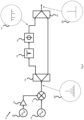
- FIG. 1 An embodiment of the present invention is shown schematically in Figure 1 .
- An oscillator 110 is provided which produces a primary output signal and a number of additional signals as lower magnitude sidebands.
- a sample spectrum is shown as 200.
- the spurious sidebands tend to be distributed symmetrically about the primary (wanted) signal and also tend to decay in magnitude at frequencies further removed from the primary signal. However, this need not be the case and any signals present which are not the primary signal are generally regarded as undesirable.
- the output from oscillator 110 is applied to signal splitter 120, which produces two substantially identical outputs form the input signal applied. Each output signal is applied to a respective signal path 120a, 120b. Path 120b is passed directly and unmodified in any way to an input of power combiner 150. Path 120a is modified by the action of notch filter 130 and phase shifter 140.
- Notch filter 130 is a filter also known as a band stop filter, more particularly a narrow band stop filter, and is arranged to remove or attenuate a range of frequencies.
- the range of frequencies is narrow and corresponds to the wanted or primary frequency produced by the oscillator 110.
- the effect of notch filter 130 is to effectively remove the wanted signal and allow only the unwanted signals to pass.
- phase shifter 140 applies a 180° phase shift and effectively inverts the signals applied thereto.
- notch filter 130 and phase shifter 140 The net result of the actions of notch filter 130 and phase shifter 140 is shown in the illustrative spectrum 210 which shows the signals present at the output of the phase shifter 140. Note the absence of the central primary frequency and the inversion of the unwanted sidebands.
- the notch filter 130 should be relatively fast-tuning and should be calibrated for each of possibly several STALO frequencies which are required at the output of the STALO 100.
- the phase shifter 140 also requires calibration for each of the possibly several STALO frequencies. Details of the calibration process are provided later in connection with Figure 3 .
- the respective path lengths of signal paths 120a and 120b should be substantially identical, hence the need for the calibration referred to above. Proper calibration ensure an optimal result.
- the notch filter 130 and phase shifter 140 although shown in Figure 1 as the notch filter acting before the phase shifter, the order of operation can be inverted i.e. the phase shifter 140 can be positioned before the notch filter 130, such that it acts first.
- the net effect in either case is identical, with the spectrum 210 at the first input to power combiner 150 being the same regardless of the sequence of operation of the notch filter 130 and phase shifter 140.
- Power combiner 150 has two inputs. As mentioned previously, one input is from signal path 120b and is an unmodified output from power splitter 120. The other input is derived from signal path 120a, as described immediately above.
- Power combiner 150 acts to sum the two signals applied to its inputs.
- the two spectrums illustrated at 200 and 210 are summed such that the inverted unwanted sideband signals are effectively subtracted from the original spectrum, leaving only the wanted central frequency.
- the output of combiner 150 is shown a spectrum 220, consisting of only the wanted central frequency.
- oscillator 110 may be any suitable nominally single frequency source, such as, but not limited to, a Voltage Controlled Oscillator (VCO), Digital to Analog Convertor (DAC), Arbitrary Waveform Generator, Direct Digital Synthesiser (DDS), Signal Generator, Voltage Controlled Crystal Oscillator (VCXO), Oven Controlled Crystal Oscillator (OCXO), Numerically Controlled Oscillator (NCO), Dielectric Resonating Oscillator (DRO) or Frequency Multiplier.
- VCO Voltage Controlled Oscillator
- DAC Digital to Analog Convertor
- DDS Direct Digital Synthesiser
- VCO Voltage Controlled Crystal Oscillator
- OCXO Oven Controlled Crystal Oscillator
- NCO Numerically Controlled Oscillator
- DRO Dielectric Resonating Oscillator
- COTS Commercial Off the Shelf
- the Power Divider 120 and Power Combiner could be Mini-Circuits EP2W+.
- the coupler 200 could be Mini-Circuits BDCA-16-30+.
- the phase shifter 140 could be Qorvo TGP2108-SM.
- the notch filter could be Atlanta Microwave AM3129.
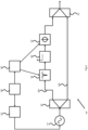
- Figure 2 shows a second embodiment of the present invention, which differs slightly to the first embodiment of Figure 1 , but only in the earlier stages before the power splitter 120. All subsequent operations are identical with those described in relation to Figure 1 and so are not repeated for reasons of brevity.
- the STALO 101 shows a structure including a pair of signal sources which are mixed to produce a signal which is then provided to power splitter 120 as an input signal.
- a structure is used wherein one of the two signal sources is a local oscillator (LO) and the other is a Radio Frequency (RF) or Intermediate Frequency (IF) oscillator.
- LO local oscillator
- RF Radio Frequency
- IF Intermediate Frequency
- Signal source 124 produces a signal which is mixed with the signal produced from signal source 126 in mixer 112.
- Mixer 112 uses an inherently non-linear process to multiply the signals and so even if the outputs of signal sources 124 and 126 are ideal and include only a single frequency, the output of mixer 112 will inevitably include some unwanted sideband signals as described previously and illustrated in spectrum 200, as before.
- signal source 124 produces the RF or IF signal and signal source 126 produces the LO signal. Note that the output of signal source 126 may be amplified if required by amplifier 128.
- the input to signal splitter 120 typically comprises a plurality of signals forming a spectrum including a wanted and several unwanted signals at discrete frequencies.
- Figure 3 shows a slightly different version 100' of the first embodiment of Figure 1 , incorporating additional elements which are provided for the purpose of tuning and/or calibration. Like-numbered elements are as described previously.
- the additional components relate only to the tuning and/or calibration of the system and are not normally required during normal operation.
- Frequency controller 220 is arranged to control the frequency of the desired output frequency. It, in turn, provides a signal to oscillator controller 210, which directly controls the signal source or oscillator 110. At the same time, the frequency controller 220 interfaces with the calibration data store 230, which stores certain parameters associated with the calibration, as will be described. The calibration data store interfaces with the notch filter 130 and phase shifter 140.
- test coupler 200 Provided immediately after the notch filter 130 is a test coupler 200, which samples the output of the notch filter directly.
- the calibration process involves the frequency controller 220 setting a centre frequency of operation, F c .
- the output of the notch filter 130 is measured by the test coupler 200, with the notch filter control voltage set to a minimum.
- the path lengths between power splitter 120 and the power combiner 150, operating at F c should be adjusted to be phase matched when the notch filter is set to F c and the phase shifter 140 is set to 0°.
- the notch filter 130 control voltage is adjusted to achieve maximum suppression of the carrier frequency as seen at the output of the test coupler 200.
- the phase shifter 140 is adjusted to achieve the maximum suppression of spurious signals, as measured at the output of the power combiner 150.
- values of notch control voltage and phase shifter settings are saved for F c .
- This process is then repeated for one or more other output frequencies, whereby the relevant values for the notch filter control voltage and phase shifter settings are stored for each frequency of interest.
- the notch filter 130 and phase shifter 140 can be configured using values stored in the calibration data store 230 for any desired frequency of interest.
- oscillator controller 210 is arranged to provide separate control signals to the two oscillators 124, 126.
- FIG. 4 shows a flowchart illustrating steps involved in an embodiment of the invention.
- an input signal to power splitter 120 is split into two substantially identical components.
- the first of the two components is notch filtered by notch filter 130 to remove a frequency component at a desired frequency.
- the notch filtered signal is then phase shifted by 180° to produce a signal for inputting to power combiner 150.
- step S106 the output from step S104 is combined in power combiner 150 with the second of the two components from step S100 to yield a desired output signal which comprises substantially the desired signal only.
Landscapes
- Stabilization Of Oscillater, Synchronisation, Frequency Synthesizers (AREA)
Abstract
Disclosed is an oscillator system for producing an RF output signal, comprising: a first signal source arranged to output a first signal at a first frequency; a signal splitter to split the first signal into a first component signal and a substantially identical second component signal; a notch filter and a 180° phase shifter arranged in a signal path of the first component signal, arranged with either the notch filter or the phase shifter acting first and the other acting second, to produce a modified first component signal; and a signal combiner arranged to combine the second component signal and the modified first component signal to produce the RF output signal.
Description
- The present invention relates to an improved oscillator design. It finds particular application where a Stabilised Local Oscillator (STALO) is required, but may be used in other, more general, applications. One particular application of interest is in the field of RADAR design, where stable, low phase noise signals having low spurious output components is of particular importance. Such a STALO can provide significant performance improvements over a non-STALO design.
- The design of a Stabilised Local Oscillator (STALO) requires the production of low phase noise, low spurious output signals used to provide the local oscillator signals for the double super-heterodyne up-conversion and down-conversion RF processing required within a radar system.
- The RF processing primarily uses mixers to provide either the upper or lower side-band signals required by the RF up or down converters. Mixers are non-linear devices and generate additional signals related to the local oscillator signal and the RF input frequency.
- The equation below defines the expected output frequencies, F, from the mixer (where FR is the RF frequency and FL is the local oscillator frequency):

- m = 1,2,3...
- n = 1,2,3 ...
- These mixer products are predictable within the design of the frequency plan. However, there are occasions when the operational frequency bands are limited and these mixer spurs can be problematic. It is an aim of an embodiment of the present invention to address these shortcomings in the prior art and provide an oscillator having a "cleaner" output spectrum. Ideally, an output should have no spurs at all. This is practically impossible and so an aim is to reduce the magnitude of any spurs significantly.
- According to a first aspect of the present invention, there is provided an oscillator system for producing an RF output signal, comprising: a first signal source arranged to output a first signal at a first frequency; a signal splitter to split the first signal into a first component signal and a substantially identical second component signal; a notch filter and a 180° phase shifter arranged in a signal path of the first component signal, arranged with either the notch filter or the phase shifter acting first and the other acting second, to produce a modified first component signal; and a signal combiner arranged to combine the second component signal and the modified first component signal to produce the RF output signal.
- In an embodiment, the first signal source is one of a Voltage Controlled Oscillator ,VCO, Digital to Analog Convertor, DAC, Arbitrary Waveform Generator, Direct Digital Synthesiser, DDS, Signal Generator, Voltage Controlled Crystal Oscillator, VCXO, Oven Controlled Crystal Oscillator, OCXO, Numerically Controlled Oscillator, NCO, Dielectric Resonating Oscillator, DRO, or Frequency Multiplier, VCO, DDS, DAC, a mixer [any others?]
- In an embodiment, the first signal source is a mixer which is arranged to output the first signal, the oscillator system further comprising a second signal source arranged to output a second signal at a second frequency and a third signal source arranged to output a third signal at a third frequency, whereby the second and third signals are mixed in the mixer to produce the first signal.
- In an embodiment, the second and third signal sources are each one of a Voltage Controlled Oscillator ,VCO, Digital to Analog Convertor, DAC, Arbitrary Waveform Generator, Direct Digital Synthesiser, DDS, Signal Generator, Voltage Controlled Crystal Oscillator, VCXO, Oven Controlled Crystal Oscillator, OCXO, Numerically Controlled Oscillator, NCO, Dielectric Resonating Oscillator, DRO, a mixer or Frequency MultiplierVCO, DDS, DAC, a mixer [any others?].
- In an embodiment, the second signal is a local oscillator signal and the third signal is an RF or IF signal.
- In an embodiment, there is further provided a calibration data store, operable to store a plurality of calibration parameters associated with respective frequencies of operation, said plurality of calibration parameters being used to configure at least one component of the oscillator system.
- According to a second aspect of the present invention, there is provided a method of providing a desired signal comprising a component having a single desired frequency, comprising the steps of: providing an input signal comprising the desired frequency as well as at least one unwanted frequency; splitting the input signal into substantially identical first and second components; notch filtering and 180° phase shifting the first component to produce a modified first component; combining the modified first component and the second component to provide the desired signal.
- Embodiments of the invention will now be described by way of example only with reference to the figures, in which:
-
Figure 1 shows a schematic representation of a first embodiment of the present invention; -
Figure 2 shows a schematic representation of a second embodiment of the present invention; -
Figure 3 shows a more detailed schematic representation of a first embodiment of the present invention, including tuning/calibration elements; and -
Figure 4 shows a flowchart illustrating a method according to an embodiment of the present invention. - An embodiment of the present invention is shown schematically in
Figure 1 . This shows aSTALO 100 comprising various component parts, the operation of which will be described below. - An
oscillator 110 is provided which produces a primary output signal and a number of additional signals as lower magnitude sidebands. A sample spectrum is shown as 200. The spurious sidebands tend to be distributed symmetrically about the primary (wanted) signal and also tend to decay in magnitude at frequencies further removed from the primary signal. However, this need not be the case and any signals present which are not the primary signal are generally regarded as undesirable. - The output from
oscillator 110 is applied tosignal splitter 120, which produces two substantially identical outputs form the input signal applied. Each output signal is applied to arespective signal path Path 120a is modified by the action ofnotch filter 130 andphase shifter 140. -
Notch filter 130 is a filter also known as a band stop filter, more particularly a narrow band stop filter, and is arranged to remove or attenuate a range of frequencies. Preferably, the range of frequencies is narrow and corresponds to the wanted or primary frequency produced by theoscillator 110. The effect ofnotch filter 130 is to effectively remove the wanted signal and allow only the unwanted signals to pass. - These unwanted signals or sidebands are then passed to a
phase shifter 140. Specifically thephase shifter 140 applies a 180° phase shift and effectively inverts the signals applied thereto. - The net result of the actions of
notch filter 130 andphase shifter 140 is shown in theillustrative spectrum 210 which shows the signals present at the output of thephase shifter 140. Note the absence of the central primary frequency and the inversion of the unwanted sidebands. - The
notch filter 130 should be relatively fast-tuning and should be calibrated for each of possibly several STALO frequencies which are required at the output of the STALO 100. Thephase shifter 140 also requires calibration for each of the possibly several STALO frequencies. Details of the calibration process are provided later in connection withFigure 3 . - The respective path lengths of
signal paths - At this point, it is important to note that the
notch filter 130 andphase shifter 140 although shown inFigure 1 as the notch filter acting before the phase shifter, the order of operation can be inverted i.e. thephase shifter 140 can be positioned before thenotch filter 130, such that it acts first. The net effect in either case is identical, with thespectrum 210 at the first input to power combiner 150 being the same regardless of the sequence of operation of thenotch filter 130 andphase shifter 140. - Power combiner 150 has two inputs. As mentioned previously, one input is from
signal path 120b and is an unmodified output frompower splitter 120. The other input is derived fromsignal path 120a, as described immediately above. - Power combiner 150 acts to sum the two signals applied to its inputs. The two spectrums illustrated at 200 and 210 are summed such that the inverted unwanted sideband signals are effectively subtracted from the original spectrum, leaving only the wanted central frequency. The output of
combiner 150 is shown aspectrum 220, consisting of only the wanted central frequency. - Note that
oscillator 110 may be any suitable nominally single frequency source, such as, but not limited to, a Voltage Controlled Oscillator (VCO), Digital to Analog Convertor (DAC), Arbitrary Waveform Generator, Direct Digital Synthesiser (DDS), Signal Generator, Voltage Controlled Crystal Oscillator (VCXO), Oven Controlled Crystal Oscillator (OCXO), Numerically Controlled Oscillator (NCO), Dielectric Resonating Oscillator (DRO) or Frequency Multiplier. - The majority of individual components referred to herein are available as Commercial Off the Shelf, COTS, components. By way of example only, the following are examples of suitable components, noting that this is not intended to be an exhaustive list and neither does it preclude the possibility of designing and procuring bespoke devices, as desired.
- The
Power Divider 120 and Power Combiner could be Mini-Circuits EP2W+. Thecoupler 200 could be Mini-Circuits BDCA-16-30+. Thephase shifter 140 could be Qorvo TGP2108-SM. The notch filter could be Atlanta Microwave AM3129. -
Figure 2 shows a second embodiment of the present invention, which differs slightly to the first embodiment ofFigure 1 , but only in the earlier stages before thepower splitter 120. All subsequent operations are identical with those described in relation toFigure 1 and so are not repeated for reasons of brevity. - In the embodiment of
Figure 2 , theSTALO 101 shows a structure including a pair of signal sources which are mixed to produce a signal which is then provided topower splitter 120 as an input signal. Such a structure is used wherein one of the two signal sources is a local oscillator (LO) and the other is a Radio Frequency (RF) or Intermediate Frequency (IF) oscillator. - Signal
source 124 produces a signal which is mixed with the signal produced fromsignal source 126 inmixer 112.Mixer 112 uses an inherently non-linear process to multiply the signals and so even if the outputs ofsignal sources mixer 112 will inevitably include some unwanted sideband signals as described previously and illustrated inspectrum 200, as before. - Note that
signal source 124 produces the RF or IF signal and signalsource 126 produces the LO signal. Note that the output ofsignal source 126 may be amplified if required byamplifier 128. - The similarity between the first and second embodiments is that the input to signal
splitter 120 typically comprises a plurality of signals forming a spectrum including a wanted and several unwanted signals at discrete frequencies. -
Figure 3 shows a slightly different version 100' of the first embodiment ofFigure 1 , incorporating additional elements which are provided for the purpose of tuning and/or calibration. Like-numbered elements are as described previously. The additional components relate only to the tuning and/or calibration of the system and are not normally required during normal operation. -
Frequency controller 220 is arranged to control the frequency of the desired output frequency. It, in turn, provides a signal tooscillator controller 210, which directly controls the signal source oroscillator 110. At the same time, thefrequency controller 220 interfaces with thecalibration data store 230, which stores certain parameters associated with the calibration, as will be described. The calibration data store interfaces with thenotch filter 130 andphase shifter 140. - Provided immediately after the
notch filter 130 is atest coupler 200, which samples the output of the notch filter directly. - The calibration process involves the
frequency controller 220 setting a centre frequency of operation, Fc. The output of thenotch filter 130 is measured by thetest coupler 200, with the notch filter control voltage set to a minimum. The path lengths betweenpower splitter 120 and thepower combiner 150, operating at Fc should be adjusted to be phase matched when the notch filter is set to Fc and thephase shifter 140 is set to 0°. - Then, the
notch filter 130 control voltage is adjusted to achieve maximum suppression of the carrier frequency as seen at the output of thetest coupler 200. Thephase shifter 140 is adjusted to achieve the maximum suppression of spurious signals, as measured at the output of thepower combiner 150. At this point, values of notch control voltage and phase shifter settings are saved for Fc. - This process is then repeated for one or more other output frequencies, whereby the relevant values for the notch filter control voltage and phase shifter settings are stored for each frequency of interest.
- In this way, the
notch filter 130 andphase shifter 140 can be configured using values stored in thecalibration data store 230 for any desired frequency of interest. - Note that a similar arrangement may be provided for the embodiment of
Figure 2 . The only substantive difference is that theoscillator controller 210 is arranged to provide separate control signals to the twooscillators -
Figure 4 shows a flowchart illustrating steps involved in an embodiment of the invention. At step S100, an input signal topower splitter 120 is split into two substantially identical components. - At step S102, the first of the two components is notch filtered by
notch filter 130 to remove a frequency component at a desired frequency. - At step S104, the notch filtered signal is then phase shifted by 180° to produce a signal for inputting to
power combiner 150. - At step S106, the output from step S104 is combined in
power combiner 150 with the second of the two components from step S100 to yield a desired output signal which comprises substantially the desired signal only.
Claims (7)
- An oscillator system for producing an RF output signal, comprising:a first signal source arranged to output a first signal at a first frequency;a signal splitter to split the first signal into a first component signal and a substantially identical second component signal;a notch filter and a 180° phase shifter arranged in a signal path of the first component signal, arranged with either the notch filter or the phase shifter acting first and the other acting second, to produce a modified first component signal; anda signal combiner arranged to combine the second component signal and the modified first component signal to produce the RF output signal.
- The oscillator system of claim 1 wherein the first signal source is one of a Voltage Controlled Oscillator ,VCO, Digital to Analog Convertor, DAC, Arbitrary Waveform Generator, Direct Digital Synthesiser, DDS, Signal Generator, Voltage Controlled Crystal Oscillator, VCXO, Oven Controlled Crystal Oscillator, OCXO, Numerically Controlled Oscillator, NCO, Dielectric Resonating Oscillator, DRO, or Frequency Multiplier.
- The oscillator system of claim 2 wherein the first signal source is a mixer which is arranged to output the first signal, the oscillator system further comprising a second signal source arranged to output a second signal at a second frequency and a third signal source arranged to output a third signal at a third frequency, whereby the second and third signals are mixed in the mixer to produce the first signal.
- The oscillator system of claim 3 wherein the second and third signal sources are each one of a Voltage Controlled Oscillator ,VCO, Digital to Analog Convertor, DAC, Arbitrary Waveform Generator, Direct Digital Synthesiser, DDS, Signal Generator, Voltage Controlled Crystal Oscillator, VCXO, Oven Controlled Crystal Oscillator, OCXO, Numerically Controlled Oscillator, NCO, Dielectric Resonating Oscillator, DRO, a mixer or Frequency Multiplier
- The oscillator system of claim 3 or 4 wherein the second signal is a local oscillator signal and the third signal is an RF or IF signal.
- The oscillator system of any preceding claim further comprising a calibration data store, operable to store a plurality of calibration parameters associated with respective frequencies of operation, said plurality of calibration parameters being used to configure at least one component of the oscillator system.
- A method of providing a desired signal comprising a component having a single desired frequency, comprising the steps of:providing an input signal comprising the desired frequency as well as at least one unwanted frequency;splitting the input signal into substantially identical first and second components;notch filtering and 180° phase shifting the first component to produce a modified first component;combining the modified first component and the second component to provide the desired signal.
Priority Applications (1)
| Application Number | Priority Date | Filing Date | Title |
|---|---|---|---|
| EP23275101.6A EP4489299A1 (en) | 2023-07-07 | 2023-07-07 | Improvements in and relating to oscillators |
Applications Claiming Priority (1)
| Application Number | Priority Date | Filing Date | Title |
|---|---|---|---|
| EP23275101.6A EP4489299A1 (en) | 2023-07-07 | 2023-07-07 | Improvements in and relating to oscillators |
Publications (1)
| Publication Number | Publication Date |
|---|---|
| EP4489299A1 true EP4489299A1 (en) | 2025-01-08 |
Family
ID=87202150
Family Applications (1)
| Application Number | Title | Priority Date | Filing Date |
|---|---|---|---|
| EP23275101.6A Ceased EP4489299A1 (en) | 2023-07-07 | 2023-07-07 | Improvements in and relating to oscillators |
Country Status (1)
| Country | Link |
|---|---|
| EP (1) | EP4489299A1 (en) |
Citations (3)
| Publication number | Priority date | Publication date | Assignee | Title |
|---|---|---|---|---|
| US6151373A (en) * | 1997-04-03 | 2000-11-21 | At&T Corp. | Weak signal resolver |
| GB2500067A (en) * | 2012-03-09 | 2013-09-11 | Renesas Mobile Corp | An N-path filter for notching out unwanted signals in wireless receivers |
| EP2056481B1 (en) * | 2007-10-31 | 2016-12-28 | Broadcom Corporation | Radio frequency filtering technique with auto calibrated stop-band rejection |
-
2023
- 2023-07-07 EP EP23275101.6A patent/EP4489299A1/en not_active Ceased
Patent Citations (3)
| Publication number | Priority date | Publication date | Assignee | Title |
|---|---|---|---|---|
| US6151373A (en) * | 1997-04-03 | 2000-11-21 | At&T Corp. | Weak signal resolver |
| EP2056481B1 (en) * | 2007-10-31 | 2016-12-28 | Broadcom Corporation | Radio frequency filtering technique with auto calibrated stop-band rejection |
| GB2500067A (en) * | 2012-03-09 | 2013-09-11 | Renesas Mobile Corp | An N-path filter for notching out unwanted signals in wireless receivers |
Similar Documents
| Publication | Publication Date | Title |
|---|---|---|
| US7701299B2 (en) | Low phase noise PLL synthesizer | |
| US5317284A (en) | Wide band, low noise, fine step tuning, phase locked loop frequency synthesizer | |
| US9793904B1 (en) | System and method of noise correcting PLL frequency synthesizers | |
| US4198604A (en) | Heterodyne phase lock system | |
| US5451910A (en) | Frequency synthesizer with comb spectrum mixer and fractional comb frequency offset | |
| CA2879231C (en) | Ultra low phase noise signal source | |
| US6057690A (en) | Automatic testing device for signal evaluation | |
| EP2983454B1 (en) | Single tone RF signal generator | |
| NO302599B1 (en) | Frequency synthesizer and method thereof | |
| US4673891A (en) | Frequency synthesizer having first phase locked loop frequency multiplied by near unity in second phase locked loop | |
| EP0315940B1 (en) | Apparatus and method for phase noise and post tuning drift cancellation | |
| US12123968B2 (en) | Systems and methods for digital signal chirp generation using frequency multipliers | |
| US7928808B2 (en) | Selectable local oscillator | |
| US20020176528A1 (en) | Frequency converter arrangement | |
| US6806746B1 (en) | Direct frequency synthesizer for offset loop synthesizer | |
| US4845443A (en) | Low noise multi-band channelized microwave frequency synthesizer | |
| EP4742528A1 (en) | High-frequency signal generating device | |
| JPS5994076A (en) | Spectrum analyser | |
| GB2130827A (en) | Frequency synthesizer | |
| RU2834405C1 (en) | Low-noise frequency synthesizer design with low level of side spectral components | |
| US20040027205A1 (en) | Local oscillator apparatus for low-noise generation of arbitrary frequencies | |
| EP1055129A1 (en) | Phase noise measurement system | |
| EP1204201B1 (en) | Apparatus and method for producing an RF transmision signal | |
| US2880313A (en) | Crystal oscillator isolation means | |
| JPH0760976B2 (en) | Signal suppressor |
Legal Events
| Date | Code | Title | Description |
|---|---|---|---|
| PUAI | Public reference made under article 153(3) epc to a published international application that has entered the european phase |
Free format text: ORIGINAL CODE: 0009012 |
|
| STAA | Information on the status of an ep patent application or granted ep patent |
Free format text: STATUS: THE APPLICATION HAS BEEN PUBLISHED |
|
| AK | Designated contracting states |
Kind code of ref document: A1 Designated state(s): AL AT BE BG CH CY CZ DE DK EE ES FI FR GB GR HR HU IE IS IT LI LT LU LV MC ME MK MT NL NO PL PT RO RS SE SI SK SM TR |
|
| STAA | Information on the status of an ep patent application or granted ep patent |
Free format text: STATUS: THE APPLICATION HAS BEEN REFUSED |
|
| 18R | Application refused |
Effective date: 20250325 |