EP4489278A1 - Resonant hybrid flyback converter and method of operating the same - Google Patents
Resonant hybrid flyback converter and method of operating the same Download PDFInfo
- Publication number
- EP4489278A1 EP4489278A1 EP23183785.7A EP23183785A EP4489278A1 EP 4489278 A1 EP4489278 A1 EP 4489278A1 EP 23183785 A EP23183785 A EP 23183785A EP 4489278 A1 EP4489278 A1 EP 4489278A1
- Authority
- EP
- European Patent Office
- Prior art keywords
- side switch
- converter
- low
- duration
- conduction phase
- Prior art date
- Legal status (The legal status is an assumption and is not a legal conclusion. Google has not performed a legal analysis and makes no representation as to the accuracy of the status listed.)
- Pending
Links
Images




Classifications
-
- H—ELECTRICITY
- H02—GENERATION; CONVERSION OR DISTRIBUTION OF ELECTRIC POWER
- H02M—APPARATUS FOR CONVERSION BETWEEN AC AND AC, BETWEEN AC AND DC, OR BETWEEN DC AND DC, AND FOR USE WITH MAINS OR SIMILAR POWER SUPPLY SYSTEMS; CONVERSION OF DC OR AC INPUT POWER INTO SURGE OUTPUT POWER; CONTROL OR REGULATION THEREOF
- H02M1/00—Details of apparatus for conversion
- H02M1/36—Means for starting or stopping converters
-
- H—ELECTRICITY
- H02—GENERATION; CONVERSION OR DISTRIBUTION OF ELECTRIC POWER
- H02M—APPARATUS FOR CONVERSION BETWEEN AC AND AC, BETWEEN AC AND DC, OR BETWEEN DC AND DC, AND FOR USE WITH MAINS OR SIMILAR POWER SUPPLY SYSTEMS; CONVERSION OF DC OR AC INPUT POWER INTO SURGE OUTPUT POWER; CONTROL OR REGULATION THEREOF
- H02M1/00—Details of apparatus for conversion
- H02M1/32—Means for protecting converters other than automatic disconnection
-
- H—ELECTRICITY
- H02—GENERATION; CONVERSION OR DISTRIBUTION OF ELECTRIC POWER
- H02M—APPARATUS FOR CONVERSION BETWEEN AC AND AC, BETWEEN AC AND DC, OR BETWEEN DC AND DC, AND FOR USE WITH MAINS OR SIMILAR POWER SUPPLY SYSTEMS; CONVERSION OF DC OR AC INPUT POWER INTO SURGE OUTPUT POWER; CONTROL OR REGULATION THEREOF
- H02M3/00—Conversion of DC power input into DC power output
- H02M3/01—Resonant DC/DC converters
-
- H—ELECTRICITY
- H02—GENERATION; CONVERSION OR DISTRIBUTION OF ELECTRIC POWER
- H02M—APPARATUS FOR CONVERSION BETWEEN AC AND AC, BETWEEN AC AND DC, OR BETWEEN DC AND DC, AND FOR USE WITH MAINS OR SIMILAR POWER SUPPLY SYSTEMS; CONVERSION OF DC OR AC INPUT POWER INTO SURGE OUTPUT POWER; CONTROL OR REGULATION THEREOF
- H02M3/00—Conversion of DC power input into DC power output
- H02M3/22—Conversion of DC power input into DC power output with intermediate conversion into AC
- H02M3/24—Conversion of DC power input into DC power output with intermediate conversion into AC by static converters
- H02M3/28—Conversion of DC power input into DC power output with intermediate conversion into AC by static converters using discharge tubes with control electrode or semiconductor devices with control electrode to produce the intermediate AC
- H02M3/325—Conversion of DC power input into DC power output with intermediate conversion into AC by static converters using discharge tubes with control electrode or semiconductor devices with control electrode to produce the intermediate AC using devices of a triode or a transistor type requiring continuous application of a control signal
- H02M3/335—Conversion of DC power input into DC power output with intermediate conversion into AC by static converters using discharge tubes with control electrode or semiconductor devices with control electrode to produce the intermediate AC using devices of a triode or a transistor type requiring continuous application of a control signal using semiconductor devices only
- H02M3/33507—Conversion of DC power input into DC power output with intermediate conversion into AC by static converters using discharge tubes with control electrode or semiconductor devices with control electrode to produce the intermediate AC using devices of a triode or a transistor type requiring continuous application of a control signal using semiconductor devices only with automatic control of the output voltage or current, e.g. flyback converters
-
- H—ELECTRICITY
- H02—GENERATION; CONVERSION OR DISTRIBUTION OF ELECTRIC POWER
- H02M—APPARATUS FOR CONVERSION BETWEEN AC AND AC, BETWEEN AC AND DC, OR BETWEEN DC AND DC, AND FOR USE WITH MAINS OR SIMILAR POWER SUPPLY SYSTEMS; CONVERSION OF DC OR AC INPUT POWER INTO SURGE OUTPUT POWER; CONTROL OR REGULATION THEREOF
- H02M3/00—Conversion of DC power input into DC power output
- H02M3/22—Conversion of DC power input into DC power output with intermediate conversion into AC
- H02M3/24—Conversion of DC power input into DC power output with intermediate conversion into AC by static converters
- H02M3/28—Conversion of DC power input into DC power output with intermediate conversion into AC by static converters using discharge tubes with control electrode or semiconductor devices with control electrode to produce the intermediate AC
- H02M3/325—Conversion of DC power input into DC power output with intermediate conversion into AC by static converters using discharge tubes with control electrode or semiconductor devices with control electrode to produce the intermediate AC using devices of a triode or a transistor type requiring continuous application of a control signal
- H02M3/335—Conversion of DC power input into DC power output with intermediate conversion into AC by static converters using discharge tubes with control electrode or semiconductor devices with control electrode to produce the intermediate AC using devices of a triode or a transistor type requiring continuous application of a control signal using semiconductor devices only
- H02M3/33569—Conversion of DC power input into DC power output with intermediate conversion into AC by static converters using discharge tubes with control electrode or semiconductor devices with control electrode to produce the intermediate AC using devices of a triode or a transistor type requiring continuous application of a control signal using semiconductor devices only having several active switching elements
- H02M3/33571—Half-bridge at primary side of an isolation transformer
Definitions
- the present disclosure relates generally to the field of lighting technology, and in particular to a resonant hybrid flyback converter for LED loads and to a method of operating said converter.
- Resonant hybrid flyback converters typically comprise a high-side switch and a low-side switch arranged in series (see FIG. 1 ) and driven (i.e., being conductive) alternatingly so as to induce an oscillation-based power supply via a resonant tank circuit and a galvanic separation.
- a duration of a conduction phase of the high-side switch may be manipulated by a closed-loop controller in accordance with a regulated target output/load/LED current (corresponding to a regulated target input peak current) of the converter, and a duration of a conduction phase of the low-side switch should be set in accordance with an output/load/LED voltage of the converter, i.e., depending on the load.
- the start-up of an LED converter may involve a progressive ramp-down of the duration of the conduction phase of the low-side switch starting from a predefined initial duration, until the converter supplies a predefined target output voltage corresponding to the load (see FIG. 2 ).
- the relatively slow closed-loop regulation of the output current may not be able to compensate for peak currents due to the ramp-down operation. Accordingly, every start-up of the converter may entail visible flicker.
- a resonant hybrid flyback converter comprising inductively coupled primary-side and secondary-side circuits; the primary-side circuit comprising a high-side switch and a low-side switch arranged in series; and a control circuit.
- the control circuit is operable to progressively ramp down a predefined initial duration of the conduction phase of the low-side switch until the converter supplies a predefined target output voltage; save the down-ramped duration of the conduction phase of the low-side switch; alternatingly drive the high-side switch and the low-side switch in accordance with an adjustable duration of the conduction phase of the high-side switch in accordance with a regulated target input peak current of the converter, and the saved duration of the conduction phase of the low-side switch; recall the saved duration of the conduction phase of the low-side switch following an interruption of operation of the converter; and proceed to the alternating drive operation.
- the control circuit may further be operable to recall the saved duration of the conduction phase of the low-side switch for use as the predefined initial duration following an interruption of the operation of the converter; and to proceed to the progressive ramp down operation.
- the control circuit may further be operable to delete the saved duration of the conduction phase of the low-side switch following an error condition; and to proceed to the progressive ramp down operation.
- the error condition may comprise one or more of an error shutdown of the converter, and an error of a load.
- the control circuit may further be operable to receive the saved duration of the conduction phase of the low-side switch via a management signaling; and to proceed to the alternating drive operation.
- the primary-side circuit may further comprise a resonant tank circuit arranged between a common electric potential of the high-side and low-side switches and a ground electric potential.
- the secondary-side circuit may comprise a current rectifying element, such as a diode.
- the secondary-side circuit may further comprise a voltage smoothing element, such as a smoothing capacitor.
- the control circuit may comprise a proportional-integral, PI, closed-loop controller.
- the high-side and low-side switches may comprise field effect transistors, FETs.
- a method of operating a resonant hybrid flyback converter comprises inductively coupled primary-side and secondary-side circuits; and the primary-side circuit comprises a high-side switch and a low-side switch arranged in series.
- the method comprises progressively ramping down a predefined initial duration of the conduction phase of the low-side switch until the converter supplies a predefined target output voltage; saving the down-ramped duration of the conduction phase of the low-side switch; alternatingly driving the high-side switch and the low-side switch in accordance with an adjustable duration of the conduction phase of the high-side switch in accordance with a regulated target input peak current of the converter, and the saved duration of the conduction phase of the low-side switch; recalling the saved duration of the conduction phase of the low-side switch following an interruption of operation of the converter; and proceeding to the alternatingly driving step.
- the method may be performed by the converter of the first aspect.
- a disclosure in connection with a described method may also hold true for a corresponding apparatus or system configured to perform the method and vice versa.
- a corresponding device may include one or a plurality of units, e.g. functional units, to perform the described one or plurality of method steps (e.g. one unit performing the one or plurality of steps, or a plurality of units each performing one or more of the plurality of steps), even if such one or more units are not explicitly described or illustrated in the figures.
- a specific apparatus is described based on one or a plurality of units, e.g.
- a corresponding method may include one step to perform the functionality of the one or plurality of units (e.g. one step performing the functionality of the one or plurality of units, or a plurality of steps each performing the functionality of one or more of the plurality of units), even if such one or plurality of steps are not explicitly described or illustrated in the figures. Further, it is understood that the features of the various exemplary implementations and/or aspects described herein may be combined with each other, unless specifically noted otherwise.
- FIG. 1 schematically illustrates a circuit topology of a resonant hybrid flyback converter 1 in accordance with the present disclosure.
- the converter 1 is connectable to a load 124 comprising a light-emitting diode, LED.
- the load 124 receives an output/load/LED voltage V LED and an output/load/LED current I LED .
- the converter 1 comprises inductively coupled primary-side and secondary-side circuits 11, 12, whereas the terms 'primary' and 'secondary' indicate different ground electric potentials.
- the primary-side circuit 11 comprises a high-side switch 111 and a low-side switch 112 arranged in series, i.e., a half-bridge switching circuit, whereas the term indicates a connectivity to a high electric potential and the term 'low-side' indicates a connectivity to a lower electric potential such as a ground electric potential.
- the high-side and low-side switches 111, 112 may comprise field effect transistors, FETs (see FIG. 1 ) or bipolar junction transistors, BJTs (not shown).
- the half-bridge switching circuit receives an input/bus voltage V IN and an input current I IN .
- the primary-side circuit 11 may further comprise a resonant tank circuit 114 arranged between a common electric potential of the high-side and low-side switches 111, 112 and a ground electric potential of the primary-side circuit 11.
- the resonant tank circuit 114 comprises an LLC circuit including a resonance choke 1141 (either a separate component, or an air gap forming part of a transformer that achieves the inductive coupling of the primary-side and secondary-side circuits 11, 12), a main inductance 1142, and a resonance capacitor 1143.
- a resonance choke 1141 either a separate component, or an air gap forming part of a transformer that achieves the inductive coupling of the primary-side and secondary-side circuits 11, 12
- main inductance 1142 e.g., a resonance choke 1142
- main inductance 1142 e.g., a resonance capacitor 1143
- the main inductance 1142 comprises a primary winding (not shown) of the transformer.
- the secondary-side circuit 12 comprises a secondary winding 121 of the transformer, and may further comprise a current rectifying element 122, such as a (Schottky) diode, or a switch/transistor (giving a synchronous converter) and a voltage smoothing element 123, such as a (electrolytic) smoothing capacitor.
- a current rectifying element 122 such as a (Schottky) diode, or a switch/transistor (giving a synchronous converter)
- a voltage smoothing element 123 such as a (electrolytic) smoothing capacitor.
- the primary-side circuit 11 further comprises a control circuit 113, such as an application-specific integrated circuit, ASIC, a microcontroller, ⁇ C, or the like.
- a control circuit 113 such as an application-specific integrated circuit, ASIC, a microcontroller, ⁇ C, or the like.
- control circuit 113 may comprise a proportional-integral, PI, closed-loop controller.
- PI proportional-integral
- closed-loop controller Alternatively, other known controller types such as PID may be deployed.
- the control circuit 113 is operable to progressively ramp down a predefined initial duration 221, 22, T on,ls of the conduction phase of the low-side switch 112 until the converter 1 supplies a predefined target output voltage V LED , as shown in FIG. 2 .
- the converter 1 has no information of the load 124 connected and therefore performs the progressive ramp-down operation.
- the control circuit 113 is further operable to save the down-ramped duration 222, 22, T on,ls of the conduction phase of the low-side switch 112 for future use. Accordingly, the operating point is saved when it has stabilized or when the LED driver is switched off.
- the control circuit 113 is further operable to alternatingly drive the high-side switch 111 and the low-side switch 112 - the high-side switch 111 in accordance with an adjustable duration 21, T on,hs of the conduction phase of the high-side switch 111 in accordance with a regulated target input peak current Î IN of the converter 1, and the low-side switch 112 in accordance with the saved duration 222, 22, T on,ls of the conduction phase of the low-side switch 112.
- the control circuit 113 is further operable to recall the saved duration 222, 22, T on,ls of the conduction phase of the low-side switch 112 following an interruption of operation of the converter 1, and proceed/return to the alternating drive operation.
- T on,ls right away avoids a further ramp-down of the duration 22, T on,ls of the conduction phase of the low-side switch 112. Accordingly, peak currents are avoided, which protects circuit components and avoids flicker during start-up of the converter 1. This is achieved via a simple software implementation and at no additional costs.
- the control circuit 113 may further be operable to recall the saved duration 222, 22, T on,ls of the conduction phase of the low-side switch 112 for use as the predefined initial duration 221, 22, T on,ls following an interruption of the operation of the converter 1, and to proceed to the progressive ramp down operation.
- the control circuit 113 may further be operable to delete the saved duration 222, 22, T on,ls of the conduction phase of the low-side switch 112 following an error condition, such as an error shutdown of the converter 1 and/or an error of the load 124, and to proceed to the progressive ramp down operation.
- an error condition such as an error shutdown of the converter 1 and/or an error of the load 124
- the converter 1 starts-up with wrong or non-ideal pre-configured settings. This in worst case could lead to an over current event or other error events (and flicker) which would trigger an error shutdown whereby also the pre-configured settings will be deleted.
- the control circuit 113 may further be operable to receive the saved duration 222, 22, T on,ls of the conduction phase of the low-side switch 112 via a management signaling, and to proceed to the alternating drive operation.
- This setting can also be preconfigured to the converter 1, to avoid a ramp-down of the duration 22, T on,ls of the conduction phase of the low-side switch 112 during a first start up, when needed.
- T on,ls right away avoids a (further) ramp-down of the duration 22, T on,ls of the conduction phase of the low-side switch 112. Peak currents are avoided without any initial ramp-down of the duration 22, T on,ls of the conduction phase of the low-side switch 112, which again protects circuit components and avoids flicker during start-up of the converter 1.
- FIG. 2 illustrates a progressive ramp-down of the duration 22 of the conduction phase of the low-side switch 112, versus an output/load/LED voltage VLED.
- T on,ls of the conduction phase of the low-side switch 112 therefore reduces or suppresses such start-up phases involving peak currents, which protects circuit components and avoids flicker.
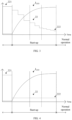
- FIG. 3 schematically illustrates the progressive ramp-down of the duration 22 of the conduction phase of the low-side switch 112, versus time.
- the duration 22, T on,ls of the conduction phase of the low-side switch 112 is set/reduced in a plurality of steps, until the converter 1 supplies a predefined target output voltage V LED (not shown), while the output current I LED ramps up.
- FIG. 4 schematically illustrates a step-down of the duration 22 of the conduction phase of the low-side switch 112 in accordance with the present disclosure, versus time.
- the duration 22 of the conduction phase of the low-side switch 112 is set/reduced to the saved duration 222, 22, T on,ls in a single step, while the output current I LED ramps up.
- FIG. 5 illustrates a known start-up operation versus time, involving the progressive ramp-down of the duration 22 of the conduction phase of the low-side switch 112.
- the duration 22 of the conduction phase of the low-side switch 112 is reduced in a plurality of steps, until the converter 1 supplies a predefined target output voltage V LED (not shown).
- the duration 21, T on,hs of the conduction phase of the high-side switch 111 experiences a transient phase including overshooting, after which it stabilizes around a constant value.
- FIG. 6 illustrates a start-up operation in accordance with the present disclosure versus time, involving the step-down of the duration 22 of the conduction phase of the low-side switch 112.
- the duration 22 of the conduction phase of the low-side switch 112 is set/reduced to the saved duration 222, 22, T on,ls in a single step.
- the duration 21, T on,hs of the conduction phase of the high-side switch 111 experiences a transient phase that involves no overshooting and is shorter than the one shown in FIG. 5 , after which it stabilizes around a constant value.
- the axis scales for the duration 21, T on,hs are different in FIG. 5 and FIG. 6 - in both cases a same value is achieved upon the transition to a normal operation.
- FIG. 7 illustrates a flow diagram of a method 3 of operating a resonant hybrid flyback converter 1 in accordance with the present disclosure.
- the method 3 may be performed by the converter 1 of the first aspect.
- the converter 1 comprises inductively coupled primary-side and secondary-side circuits 11, 12; and the primary-side circuit 11 comprises a high-side switch 111 and a low-side switch 112 arranged in series.
- the method 3 comprises a step of progressively ramping down 31 a predefined initial duration 221, 22, T on,ls of the conduction phase of the low-side switch 112 until the converter 1 supplies a predefined target output voltage VLED.
- the method 3 further comprises a step of saving 32 the down-ramped duration 222, 22, T on,ls of the conduction phase of the low-side switch 112.
- the method 3 further comprises a step of alternatingly driving 33 the high-side switch 111 and the low-side switch 112 in accordance with an adjustable duration 21, T on,hs of the conduction phase of the high-side switch 111 in accordance with a regulated target input peak current ÎN of the converter 1, and the saved duration 222, 22, T on,ls of the conduction phase of the low-side switch 112.
- the method 3 further comprises a step of recalling 34 the saved duration 222, 22, T on,ls of the conduction phase of the low-side switch 112 following an interruption of operation of the converter 1, and proceeding to the alternatingly driving step 33.
- a computer program may be stored/distributed on a suitable medium, such as an optical storage medium or a solid-state medium supplied together with or as part of other hardware, but may also be distributed in other forms, such as via the Internet or other wired or wireless telecommunication systems.
- a suitable medium such as an optical storage medium or a solid-state medium supplied together with or as part of other hardware, but may also be distributed in other forms, such as via the Internet or other wired or wireless telecommunication systems.
Landscapes
- Engineering & Computer Science (AREA)
- Power Engineering (AREA)
- Dc-Dc Converters (AREA)
Abstract
Description
- The present disclosure relates generally to the field of lighting technology, and in particular to a resonant hybrid flyback converter for LED loads and to a method of operating said converter.
- Resonant hybrid flyback converters typically comprise a high-side switch and a low-side switch arranged in series (see
FIG. 1 ) and driven (i.e., being conductive) alternatingly so as to induce an oscillation-based power supply via a resonant tank circuit and a galvanic separation. - According to common practice, a duration of a conduction phase of the high-side switch may be manipulated by a closed-loop controller in accordance with a regulated target output/load/LED current (corresponding to a regulated target input peak current) of the converter, and a duration of a conduction phase of the low-side switch should be set in accordance with an output/load/LED voltage of the converter, i.e., depending on the load.
- However, LED converters typically have no information of the load connected, despite the choice of various loads due to their wide output voltage range. Therefore, the start-up of an LED converter may involve a progressive ramp-down of the duration of the conduction phase of the low-side switch starting from a predefined initial duration, until the converter supplies a predefined target output voltage corresponding to the load (see
FIG. 2 ). - The relatively slow closed-loop regulation of the output current may not be able to compensate for peak currents due to the ramp-down operation. Accordingly, every start-up of the converter may entail visible flicker.
- It is an object to overcome the above-mentioned and other drawbacks.
- The foregoing and other objects are achieved by the features of the independent claims. Further implementation forms are apparent from the dependent claims, the description and the figures.
- According to a first aspect, a resonant hybrid flyback converter is provided, comprising inductively coupled primary-side and secondary-side circuits; the primary-side circuit comprising a high-side switch and a low-side switch arranged in series; and a control circuit. The control circuit is operable to progressively ramp down a predefined initial duration of the conduction phase of the low-side switch until the converter supplies a predefined target output voltage; save the down-ramped duration of the conduction phase of the low-side switch; alternatingly drive the high-side switch and the low-side switch in accordance with an adjustable duration of the conduction phase of the high-side switch in accordance with a regulated target input peak current of the converter, and the saved duration of the conduction phase of the low-side switch; recall the saved duration of the conduction phase of the low-side switch following an interruption of operation of the converter; and proceed to the alternating drive operation.
- The control circuit may further be operable to recall the saved duration of the conduction phase of the low-side switch for use as the predefined initial duration following an interruption of the operation of the converter; and to proceed to the progressive ramp down operation.
- The control circuit may further be operable to delete the saved duration of the conduction phase of the low-side switch following an error condition; and to proceed to the progressive ramp down operation.
- The error condition may comprise one or more of an error shutdown of the converter, and an error of a load.
- The control circuit may further be operable to receive the saved duration of the conduction phase of the low-side switch via a management signaling; and to proceed to the alternating drive operation.
- The primary-side circuit may further comprise a resonant tank circuit arranged between a common electric potential of the high-side and low-side switches and a ground electric potential.
- The secondary-side circuit may comprise a current rectifying element, such as a diode.
- The secondary-side circuit may further comprise a voltage smoothing element, such as a smoothing capacitor.
- The control circuit may comprise a proportional-integral, PI, closed-loop controller.
- The high-side and low-side switches may comprise field effect transistors, FETs.
- According to a second aspect, a method of operating a resonant hybrid flyback converter is provided. The converter comprises inductively coupled primary-side and secondary-side circuits; and the primary-side circuit comprises a high-side switch and a low-side switch arranged in series. The method comprises progressively ramping down a predefined initial duration of the conduction phase of the low-side switch until the converter supplies a predefined target output voltage; saving the down-ramped duration of the conduction phase of the low-side switch; alternatingly driving the high-side switch and the low-side switch in accordance with an adjustable duration of the conduction phase of the high-side switch in accordance with a regulated target input peak current of the converter, and the saved duration of the conduction phase of the low-side switch; recalling the saved duration of the conduction phase of the low-side switch following an interruption of operation of the converter; and proceeding to the alternatingly driving step.
- The method may be performed by the converter of the first aspect.
- The above-described aspects and implementations will now be explained with reference to the accompanying drawings, in which the same or similar reference numerals designate the same or similar elements.
- The drawings are to be regarded as being schematic representations, and elements illustrated in the drawings are not necessarily shown to scale. Rather, the various elements are represented such that their function and general purpose become apparent to those skilled in the art.
-
FIG. 1 schematically illustrates a circuit topology of a resonant hybrid flyback converter in accordance with the present disclosure; -
FIG. 2 illustrates a progressive ramp-down of the duration of the conduction phase of the low-side switch, versus an output/load/LED voltage; -
FIG. 3 schematically illustrates the progressive ramp-down of the duration of the conduction phase of the low-side switch, versus time; -
FIG. 4 schematically illustrates a step-down of the duration of the conduction phase of the low-side switch in accordance with the present disclosure, versus time; -
FIG. 5 illustrates a known start-up operation versus time, involving the progressive ramp-down of theduration 22 of the conduction phase of the low-side switch; -
FIG. 6 illustrates a start-up operation in accordance with the present disclosure versus time, involving the step-down of the duration of the conduction phase of the low-side switch; and -
FIG. 7 illustrates a flow diagram of a method of operating a resonant hybrid flyback converter in accordance with the present disclosure. - In the following description, reference is made to the accompanying drawings, which form part of the disclosure, and which show, by way of illustration, specific aspects of implementations of the present disclosure or specific aspects in which implementations of the present disclosure may be used. It is understood that implementations of the present disclosure may be used in other aspects and comprise structural or logical changes not depicted in the figures. The following detailed description, therefore, is not to be taken in a limiting sense, and the scope of the present disclosure is defined by the appended claims.
- For instance, it is understood that a disclosure in connection with a described method may also hold true for a corresponding apparatus or system configured to perform the method and vice versa. For example, if one or a plurality of specific method steps are described, a corresponding device may include one or a plurality of units, e.g. functional units, to perform the described one or plurality of method steps (e.g. one unit performing the one or plurality of steps, or a plurality of units each performing one or more of the plurality of steps), even if such one or more units are not explicitly described or illustrated in the figures. On the other hand, for example, if a specific apparatus is described based on one or a plurality of units, e.g. functional units, a corresponding method may include one step to perform the functionality of the one or plurality of units (e.g. one step performing the functionality of the one or plurality of units, or a plurality of steps each performing the functionality of one or more of the plurality of units), even if such one or plurality of steps are not explicitly described or illustrated in the figures. Further, it is understood that the features of the various exemplary implementations and/or aspects described herein may be combined with each other, unless specifically noted otherwise.
-
FIG. 1 schematically illustrates a circuit topology of a resonant hybrid flyback converter 1 in accordance with the present disclosure. - The converter 1 is connectable to a
load 124 comprising a light-emitting diode, LED. Theload 124 receives an output/load/LED voltage VLED and an output/load/LED current ILED. - The converter 1 comprises inductively coupled primary-side and secondary-
side circuits - The primary-
side circuit 11 comprises a high-side switch 111 and a low-side switch 112 arranged in series, i.e., a half-bridge switching circuit, whereas the term indicates a connectivity to a high electric potential and the term 'low-side' indicates a connectivity to a lower electric potential such as a ground electric potential. In particular, the high-side and low-side switches FIG. 1 ) or bipolar junction transistors, BJTs (not shown). The half-bridge switching circuit receives an input/bus voltage VIN and an input current IIN. - The primary-
side circuit 11 may further comprise aresonant tank circuit 114 arranged between a common electric potential of the high-side and low-side switches side circuit 11. - In the example of
FIG. 1 , theresonant tank circuit 114 comprises an LLC circuit including a resonance choke 1141 (either a separate component, or an air gap forming part of a transformer that achieves the inductive coupling of the primary-side and secondary-side circuits 11, 12), amain inductance 1142, and aresonance capacitor 1143. Alternatively, other known topologies such as LCC may be deployed. - The
main inductance 1142 comprises a primary winding (not shown) of the transformer. - The secondary-
side circuit 12 comprises asecondary winding 121 of the transformer, and may further comprise a current rectifyingelement 122, such as a (Schottky) diode, or a switch/transistor (giving a synchronous converter) and avoltage smoothing element 123, such as a (electrolytic) smoothing capacitor. - The primary-
side circuit 11 further comprises acontrol circuit 113, such as an application-specific integrated circuit, ASIC, a microcontroller, µC, or the like. - In particular, the
control circuit 113 may comprise a proportional-integral, PI, closed-loop controller. Alternatively, other known controller types such as PID may be deployed. - The
control circuit 113 is operable to progressively ramp down a predefinedinitial duration side switch 112 until the converter 1 supplies a predefined target output voltage VLED, as shown inFIG. 2 . - In other words, during a first start-up the converter 1 has no information of the
load 124 connected and therefore performs the progressive ramp-down operation. - The
control circuit 113 is further operable to save the down-rampedduration side switch 112 for future use. Accordingly, the operating point is saved when it has stabilized or when the LED driver is switched off. - The
control circuit 113 is further operable to alternatingly drive the high-side switch 111 and the low-side switch 112 - the high-side switch 111 in accordance with anadjustable duration 21, Ton,hs of the conduction phase of the high-side switch 111 in accordance with a regulated target input peak current ÎIN of the converter 1, and the low-side switch 112 in accordance with the savedduration side switch 112. - The
control circuit 113 is further operable to recall the savedduration side switch 112 following an interruption of operation of the converter 1, and proceed/return to the alternating drive operation. - This means that at further start-ups, the converter 1 then re-starts with the last settings saved.
- Starting from the saved
duration duration 22, Ton,ls of the conduction phase of the low-side switch 112. Accordingly, peak currents are avoided, which protects circuit components and avoids flicker during start-up of the converter 1. This is achieved via a simple software implementation and at no additional costs. - The
control circuit 113 may further be operable to recall the savedduration side switch 112 for use as the predefinedinitial duration - Starting the further ramp-down of the
duration 22, Ton,ls of the conduction phase of the low-side switch 112 from the savedduration initial duration - The
control circuit 113 may further be operable to delete the savedduration side switch 112 following an error condition, such as an error shutdown of the converter 1 and/or an error of theload 124, and to proceed to the progressive ramp down operation. - In the very rare case of a customer changing the
load 124, the converter 1 starts-up with wrong or non-ideal pre-configured settings. This in worst case could lead to an over current event or other error events (and flicker) which would trigger an error shutdown whereby also the pre-configured settings will be deleted. - Also, during any lamp error the saved settings will be deleted.
- Starting the further ramp-down of the
duration 22, Ton,ls of the conduction phase of the low-side switch 112 from scratch (i.e., from the predefinedinitial duration - The
control circuit 113 may further be operable to receive the savedduration side switch 112 via a management signaling, and to proceed to the alternating drive operation. - This setting can also be preconfigured to the converter 1, to avoid a ramp-down of the
duration 22, Ton,ls of the conduction phase of the low-side switch 112 during a first start up, when needed. Starting from the savedduration duration 22, Ton,ls of the conduction phase of the low-side switch 112. Peak currents are avoided without any initial ramp-down of theduration 22, Ton,ls of the conduction phase of the low-side switch 112, which again protects circuit components and avoids flicker during start-up of the converter 1. -
FIG. 2 illustrates a progressive ramp-down of theduration 22 of the conduction phase of the low-side switch 112, versus an output/load/LED voltage VLED. - Note that as the output voltage VLED increases (from left to right in
FIG. 2 ), theduration 21, Ton,hs of the conduction phase of the high-side switch 111 increases and theduration 22, Ton,ls of the conduction phase of the low-side switch 112 decreases, from the predefinedinitial duration duration - This ramp-down of the
duration 22, Ton,ls of the conduction phase of the low-side switch 112 is associated with undesirable peak currents. - Avoiding repetitive or all ramp-downs of the
duration 22, Ton,ls of the conduction phase of the low-side switch 112 therefore reduces or suppresses such start-up phases involving peak currents, which protects circuit components and avoids flicker. -
FIG. 3 schematically illustrates the progressive ramp-down of theduration 22 of the conduction phase of the low-side switch 112, versus time. - The
duration 22, Ton,ls of the conduction phase of the low-side switch 112 is set/reduced in a plurality of steps, until the converter 1 supplies a predefined target output voltage VLED (not shown), while the output current ILED ramps up. -
FIG. 4 schematically illustrates a step-down of theduration 22 of the conduction phase of the low-side switch 112 in accordance with the present disclosure, versus time. - The
duration 22 of the conduction phase of the low-side switch 112 is set/reduced to the savedduration -
FIG. 5 illustrates a known start-up operation versus time, involving the progressive ramp-down of theduration 22 of the conduction phase of the low-side switch 112. - Like in
FIG. 3 , theduration 22 of the conduction phase of the low-side switch 112 is reduced in a plurality of steps, until the converter 1 supplies a predefined target output voltage VLED (not shown). - Concurrently, the
duration 21, Ton,hs of the conduction phase of the high-side switch 111 experiences a transient phase including overshooting, after which it stabilizes around a constant value. - During said transient phase, a ramp-up of the output current ILED experiences undesirable peak currents.
-
FIG. 6 illustrates a start-up operation in accordance with the present disclosure versus time, involving the step-down of theduration 22 of the conduction phase of the low-side switch 112. - Like in
FIG. 4 , theduration 22 of the conduction phase of the low-side switch 112 is set/reduced to the savedduration - Concurrently, the
duration 21, Ton,hs of the conduction phase of the high-side switch 111 experiences a transient phase that involves no overshooting and is shorter than the one shown inFIG. 5 , after which it stabilizes around a constant value. Note that the axis scales for theduration 21, Ton,hs are different inFIG. 5 and FIG. 6 - in both cases a same value is achieved upon the transition to a normal operation. - During said transient phase, a ramp-up of the output current ILED hardly experiences undesirable peak currents.
-
FIG. 7 illustrates a flow diagram of amethod 3 of operating a resonant hybrid flyback converter 1 in accordance with the present disclosure. - The
method 3 may be performed by the converter 1 of the first aspect. - The converter 1 comprises inductively coupled primary-side and secondary-
side circuits side circuit 11 comprises a high-side switch 111 and a low-side switch 112 arranged in series. - The
method 3 comprises a step of progressively ramping down 31 a predefinedinitial duration side switch 112 until the converter 1 supplies a predefined target output voltage VLED. - The
method 3 further comprises a step of saving 32 the down-rampedduration side switch 112. - The
method 3 further comprises a step of alternatingly driving 33 the high-side switch 111 and the low-side switch 112 in accordance with anadjustable duration 21, Ton,hs of the conduction phase of the high-side switch 111 in accordance with a regulated target input peak current ÎN of the converter 1, and the savedduration side switch 112. - The
method 3 further comprises a step of recalling 34 the savedduration side switch 112 following an interruption of operation of the converter 1, and proceeding to the alternatingly drivingstep 33. - The present disclosure has been described in conjunction with various implementations as examples. However, other variations can be understood and effected by those persons skilled in the art and practicing the claimed matter, from the studies of the drawings, this disclosure and the independent claims. In the claims as well as in the description the word "comprising" does not exclude other elements or steps and the indefinite article "a" or "an" does not exclude a plurality. A single element or other unit may fulfill the functions of several entities or items recited in the claims. The mere fact that certain measures are recited in the mutual different dependent claims does not indicate that a combination of these measures cannot be used in an advantageous implementation. A computer program may be stored/distributed on a suitable medium, such as an optical storage medium or a solid-state medium supplied together with or as part of other hardware, but may also be distributed in other forms, such as via the Internet or other wired or wireless telecommunication systems.
Claims (12)
- A resonant hybrid flyback converter (1), comprisinginductively coupled primary-side and secondary-side circuits (11, 12);the primary-side circuit (11) comprising a high-side switch (111) and a low-side switch (112) arranged in series; anda control circuit (113), being operable to- progressively ramp down a predefined initial duration (221, 22, Ton,ls) of the conduction phase of the low-side switch (112) until the converter (1) supplies a predefined target output voltage (VLED);- save the down-ramped duration (222, 22, Ton,ls) of the conduction phase of the low-side switch (112);- alternatingly drive the high-side switch (111) and the low-side switch (112) in accordance with- an adjustable duration (21, Ton,hs) of the conduction phase of the high-side switch (111) in accordance with a regulated target input peak current (ÎIN) of the converter (1), and- the saved duration (222, 22, Ton,ls) of the conduction phase of the low-side switch (112);- recall the saved duration (222, 22, Ton,ls) of the conduction phase of the low-side switch (112) following an interruption of operation of the converter (1); and- proceed to the alternating drive operation.
- The converter (1) of claim 1,
the control circuit (113) further being operable to- recall the saved duration (222, 22, Ton,ls) of the conduction phase of the low-side switch (112) for use as the predefined initial duration (221, 22, Ton,ls) following an interruption of the operation of the converter (1); and- proceed to the progressive ramp down operation. - The converter (1) of claim 1 or claim 2,
the control circuit (113) further being operable to- delete the saved duration (222, 22, Ton,ls) of the conduction phase of the low-side switch (112) following an error condition; and- proceed to the progressive ramp down operation. - The converter (1) any one of the preceding claims,
the error condition comprising one or more of:- an error shutdown of the converter (1), and- an error of a load (2). - The converter (1) of any one of the preceding claims,
the control circuit (113) further being operable to- receive the saved duration (222, 22, Ton,ls) of the conduction phase of the low-side switch (112) via a management signaling; and- proceed to the alternating drive operation. - The converter (1) of any one of the preceding claims,
the primary-side circuit (11) further comprising a resonant tank circuit (114) arranged between a common electric potential of the high-side and low-side switches (111, 112) and a ground electric potential. - The converter (1) of any one of the preceding claims,
the secondary-side circuit (12) comprising a current rectifying element (122), such as a diode. - The converter (1) of any one of the preceding claims,
the secondary-side circuit (12) further comprising a voltage smoothing element (123), such as a smoothing capacitor. - The converter (1) of any one of the preceding claims,
the control circuit (113) comprising a proportional-integral, PI, closed-loop controller. - The converter (1) of any one of the preceding claims,
the high-side and low-side switches (111, 112) comprising field effect transistors, FETs. - A method (3) of operating a resonant hybrid flyback converter (1),the converter (1) comprisinginductively coupled primary-side and secondary-side circuits (11, 12); andthe primary-side circuit (11) comprising a high-side switch (111) and a low-side switch (112) arranged in series;the method (3) comprising- progressively ramping down (31) a predefined initial duration (221, 22, Ton,ls) of the conduction phase of the low-side switch (112) until the converter (1) supplies a predefined target output voltage (VLED);- saving (32) the down-ramped duration (Ton,ls) of the conduction phase of the low-side switch (112);- alternatingly driving (33) the high-side switch (111) and the low-side switch (112) in accordance with- an adjustable duration (Ton,hs) of the conduction phase of the high-side switch (111) in accordance with a regulated target input peak current (ÎIN) of the converter (1), and- the saved duration (222, 22, Ton,ls) of the conduction phase of the low-side switch (112);- recalling (34) the saved duration (222, 22, Ton,ls) of the conduction phase of the low-side switch (112) following an interruption of operation of the converter (1); and- proceeding to the alternatingly driving step.
- The method (3) of claim 11,
being performed by the converter (1) of any one of the claims 1-10.
Priority Applications (2)
| Application Number | Priority Date | Filing Date | Title |
|---|---|---|---|
| EP23183785.7A EP4489278A1 (en) | 2023-07-06 | 2023-07-06 | Resonant hybrid flyback converter and method of operating the same |
| PCT/EP2024/067178 WO2025008186A1 (en) | 2023-07-06 | 2024-06-19 | Resonant hybrid flyback converter and method of operating the same |
Applications Claiming Priority (1)
| Application Number | Priority Date | Filing Date | Title |
|---|---|---|---|
| EP23183785.7A EP4489278A1 (en) | 2023-07-06 | 2023-07-06 | Resonant hybrid flyback converter and method of operating the same |
Publications (1)
| Publication Number | Publication Date |
|---|---|
| EP4489278A1 true EP4489278A1 (en) | 2025-01-08 |
Family
ID=87157939
Family Applications (1)
| Application Number | Title | Priority Date | Filing Date |
|---|---|---|---|
| EP23183785.7A Pending EP4489278A1 (en) | 2023-07-06 | 2023-07-06 | Resonant hybrid flyback converter and method of operating the same |
Country Status (2)
| Country | Link |
|---|---|
| EP (1) | EP4489278A1 (en) |
| WO (1) | WO2025008186A1 (en) |
Citations (2)
| Publication number | Priority date | Publication date | Assignee | Title |
|---|---|---|---|---|
| US20110249473A1 (en) * | 2010-04-07 | 2011-10-13 | Silitek Electronic (Guangzhou) Co., Ltd. | Resonant converting device, and control module and method for controlling a resonant converter |
| CN114531066A (en) * | 2021-12-17 | 2022-05-24 | 海信(广东)空调有限公司 | Direct current motor, starting control method and device thereof, air conditioner and storage medium |
-
2023
- 2023-07-06 EP EP23183785.7A patent/EP4489278A1/en active Pending
-
2024
- 2024-06-19 WO PCT/EP2024/067178 patent/WO2025008186A1/en not_active Ceased
Patent Citations (2)
| Publication number | Priority date | Publication date | Assignee | Title |
|---|---|---|---|---|
| US20110249473A1 (en) * | 2010-04-07 | 2011-10-13 | Silitek Electronic (Guangzhou) Co., Ltd. | Resonant converting device, and control module and method for controlling a resonant converter |
| CN114531066A (en) * | 2021-12-17 | 2022-05-24 | 海信(广东)空调有限公司 | Direct current motor, starting control method and device thereof, air conditioner and storage medium |
Non-Patent Citations (1)
| Title |
|---|
| . .: "XDP Hybrid-flyback Controller XDPS2201", 10 June 2021 (2021-06-10), pages 1 - 75, XP093107777, Retrieved from the Internet <URL:https://www.infineon.com/dgdl/Infineon-XDPS2201-DataSheet-v01_20-EN.pdf?fileId=5546d46277921c320177b3d4ea4a2055> [retrieved on 20231201] * |
Also Published As
| Publication number | Publication date |
|---|---|
| WO2025008186A1 (en) | 2025-01-09 |
Similar Documents
| Publication | Publication Date | Title |
|---|---|---|
| KR101931448B1 (en) | System and method for a startup cell circuit | |
| CN105610328B (en) | The system and method for switched-mode power supply | |
| US8149597B2 (en) | Intermediate bus architecture with a quasi-regulated bus converter | |
| EP2449665B1 (en) | Low cost power supply circuit and method | |
| US9060397B2 (en) | High voltage LED and driver | |
| CN101164220B (en) | Power source control method and structure thereof | |
| KR20100069581A (en) | Power supply apparatus and image forming apparatus | |
| KR20010080701A (en) | Soft start scheme for resonant converters having variable frequency control | |
| JP3236587B2 (en) | Switching power supply | |
| KR20210025576A (en) | Low-voltage DC-DC Converter AND BATTERY CHARGER | |
| US20260031716A1 (en) | Soft start circuit, soft start method and power conversion system | |
| US12224668B2 (en) | Boost converter and method of controlling a boost converter | |
| JP7746691B2 (en) | Power circuit, power supply device | |
| US9723668B2 (en) | Switching converter and lighting device using the same | |
| JP5606877B2 (en) | Buck converter | |
| EP2975767A1 (en) | A switched mode power supply, a controller therefor, a lighting circuit and a control method | |
| CN115336391B (en) | LED driver and driving method | |
| JP6239242B2 (en) | Semiconductor illumination power supply control circuit, semiconductor integrated circuit, and semiconductor illumination power supply | |
| WO2025008186A1 (en) | Resonant hybrid flyback converter and method of operating the same | |
| JP2017112782A (en) | Switching power supply device | |
| JP6417844B2 (en) | Discharge lamp lighting device | |
| KR20010003072A (en) | Start-up circuit of power supply | |
| CN102843847A (en) | Driving device for fluorescent lamp tube |
Legal Events
| Date | Code | Title | Description |
|---|---|---|---|
| PUAI | Public reference made under article 153(3) epc to a published international application that has entered the european phase |
Free format text: ORIGINAL CODE: 0009012 |
|
| STAA | Information on the status of an ep patent application or granted ep patent |
Free format text: STATUS: THE APPLICATION HAS BEEN PUBLISHED |
|
| AK | Designated contracting states |
Kind code of ref document: A1 Designated state(s): AL AT BE BG CH CY CZ DE DK EE ES FI FR GB GR HR HU IE IS IT LI LT LU LV MC ME MK MT NL NO PL PT RO RS SE SI SK SM TR |
|
| STAA | Information on the status of an ep patent application or granted ep patent |
Free format text: STATUS: REQUEST FOR EXAMINATION WAS MADE |
|
| 17P | Request for examination filed |
Effective date: 20250304 |
|
| STAA | Information on the status of an ep patent application or granted ep patent |
Free format text: STATUS: EXAMINATION IS IN PROGRESS |
|
| 17Q | First examination report despatched |
Effective date: 20260224 |