EP4489218A1 - Antenna assembly, dual-frequency wideband antenna, and electronic device - Google Patents
Antenna assembly, dual-frequency wideband antenna, and electronic device Download PDFInfo
- Publication number
- EP4489218A1 EP4489218A1 EP22930660.0A EP22930660A EP4489218A1 EP 4489218 A1 EP4489218 A1 EP 4489218A1 EP 22930660 A EP22930660 A EP 22930660A EP 4489218 A1 EP4489218 A1 EP 4489218A1
- Authority
- EP
- European Patent Office
- Prior art keywords
- antenna
- radiator
- inductor
- antenna radiator
- point
- Prior art date
- Legal status (The legal status is an assumption and is not a legal conclusion. Google has not performed a legal analysis and makes no representation as to the accuracy of the status listed.)
- Pending
Links
Images



Classifications
-
- H—ELECTRICITY
- H01—ELECTRIC ELEMENTS
- H01Q—ANTENNAS, i.e. RADIO AERIALS
- H01Q5/00—Arrangements for simultaneous operation of antennas on two or more different wavebands, e.g. dual-band or multi-band arrangements
- H01Q5/20—Arrangements for simultaneous operation of antennas on two or more different wavebands, e.g. dual-band or multi-band arrangements characterised by the operating wavebands
- H01Q5/25—Ultra-wideband [UWB] systems, e.g. multiple resonance systems; Pulse systems
-
- H—ELECTRICITY
- H01—ELECTRIC ELEMENTS
- H01Q—ANTENNAS, i.e. RADIO AERIALS
- H01Q1/00—Details of, or arrangements associated with, antennas
- H01Q1/36—Structural form of radiating elements, e.g. cone, spiral, umbrella; Particular materials used therewith
- H01Q1/38—Structural form of radiating elements, e.g. cone, spiral, umbrella; Particular materials used therewith formed by a conductive layer on an insulating support
-
- H—ELECTRICITY
- H01—ELECTRIC ELEMENTS
- H01Q—ANTENNAS, i.e. RADIO AERIALS
- H01Q5/00—Arrangements for simultaneous operation of antennas on two or more different wavebands, e.g. dual-band or multi-band arrangements
- H01Q5/30—Arrangements for providing operation on different wavebands
- H01Q5/307—Individual or coupled radiating elements, each element being fed in an unspecified way
- H01Q5/314—Individual or coupled radiating elements, each element being fed in an unspecified way using frequency dependent circuits or components, e.g. trap circuits or capacitors
- H01Q5/335—Individual or coupled radiating elements, each element being fed in an unspecified way using frequency dependent circuits or components, e.g. trap circuits or capacitors at the feed, e.g. for impedance matching
-
- H—ELECTRICITY
- H01—ELECTRIC ELEMENTS
- H01Q—ANTENNAS, i.e. RADIO AERIALS
- H01Q1/00—Details of, or arrangements associated with, antennas
- H01Q1/12—Supports; Mounting means
- H01Q1/22—Supports; Mounting means by structural association with other equipment or articles
- H01Q1/24—Supports; Mounting means by structural association with other equipment or articles with receiving set
- H01Q1/241—Supports; Mounting means by structural association with other equipment or articles with receiving set used in mobile communications, e.g. GSM
-
- H—ELECTRICITY
- H01—ELECTRIC ELEMENTS
- H01Q—ANTENNAS, i.e. RADIO AERIALS
- H01Q1/00—Details of, or arrangements associated with, antennas
- H01Q1/48—Earthing means; Earth screens; Counterpoises
-
- H—ELECTRICITY
- H01—ELECTRIC ELEMENTS
- H01Q—ANTENNAS, i.e. RADIO AERIALS
- H01Q1/00—Details of, or arrangements associated with, antennas
- H01Q1/50—Structural association of antennas with earthing switches, lead-in devices or lightning protectors
-
- H—ELECTRICITY
- H01—ELECTRIC ELEMENTS
- H01Q—ANTENNAS, i.e. RADIO AERIALS
- H01Q5/00—Arrangements for simultaneous operation of antennas on two or more different wavebands, e.g. dual-band or multi-band arrangements
- H01Q5/10—Resonant antennas
-
- H—ELECTRICITY
- H01—ELECTRIC ELEMENTS
- H01Q—ANTENNAS, i.e. RADIO AERIALS
- H01Q5/00—Arrangements for simultaneous operation of antennas on two or more different wavebands, e.g. dual-band or multi-band arrangements
- H01Q5/20—Arrangements for simultaneous operation of antennas on two or more different wavebands, e.g. dual-band or multi-band arrangements characterised by the operating wavebands
-
- H—ELECTRICITY
- H01—ELECTRIC ELEMENTS
- H01Q—ANTENNAS, i.e. RADIO AERIALS
- H01Q5/00—Arrangements for simultaneous operation of antennas on two or more different wavebands, e.g. dual-band or multi-band arrangements
- H01Q5/30—Arrangements for providing operation on different wavebands
- H01Q5/307—Individual or coupled radiating elements, each element being fed in an unspecified way
-
- H—ELECTRICITY
- H01—ELECTRIC ELEMENTS
- H01Q—ANTENNAS, i.e. RADIO AERIALS
- H01Q5/00—Arrangements for simultaneous operation of antennas on two or more different wavebands, e.g. dual-band or multi-band arrangements
- H01Q5/30—Arrangements for providing operation on different wavebands
- H01Q5/307—Individual or coupled radiating elements, each element being fed in an unspecified way
- H01Q5/342—Individual or coupled radiating elements, each element being fed in an unspecified way for different propagation modes
- H01Q5/357—Individual or coupled radiating elements, each element being fed in an unspecified way for different propagation modes using a single feed point
- H01Q5/364—Creating multiple current paths
-
- H—ELECTRICITY
- H01—ELECTRIC ELEMENTS
- H01Q—ANTENNAS, i.e. RADIO AERIALS
- H01Q5/00—Arrangements for simultaneous operation of antennas on two or more different wavebands, e.g. dual-band or multi-band arrangements
- H01Q5/50—Feeding or matching arrangements for broad-band or multi-band operation
-
- H—ELECTRICITY
- H01—ELECTRIC ELEMENTS
- H01Q—ANTENNAS, i.e. RADIO AERIALS
- H01Q9/00—Electrically-short antennas having dimensions not more than twice the operating wavelength and consisting of conductive active radiating elements
- H01Q9/04—Resonant antennas
- H01Q9/0407—Substantially flat resonant element parallel to ground plane, e.g. patch antenna
- H01Q9/0414—Substantially flat resonant element parallel to ground plane, e.g. patch antenna in a stacked or folded configuration
-
- H—ELECTRICITY
- H01—ELECTRIC ELEMENTS
- H01Q—ANTENNAS, i.e. RADIO AERIALS
- H01Q9/00—Electrically-short antennas having dimensions not more than twice the operating wavelength and consisting of conductive active radiating elements
- H01Q9/04—Resonant antennas
- H01Q9/0407—Substantially flat resonant element parallel to ground plane, e.g. patch antenna
- H01Q9/0421—Substantially flat resonant element parallel to ground plane, e.g. patch antenna with a shorting wall or a shorting pin at one end of the element
-
- H—ELECTRICITY
- H01—ELECTRIC ELEMENTS
- H01Q—ANTENNAS, i.e. RADIO AERIALS
- H01Q9/00—Electrically-short antennas having dimensions not more than twice the operating wavelength and consisting of conductive active radiating elements
- H01Q9/04—Resonant antennas
- H01Q9/16—Resonant antennas with feed intermediate between the extremities of the antenna, e.g. centre-fed dipole
- H01Q9/26—Resonant antennas with feed intermediate between the extremities of the antenna, e.g. centre-fed dipole with folded element or elements, the folded parts being spaced apart a small fraction of operating wavelength
-
- H—ELECTRICITY
- H01—ELECTRIC ELEMENTS
- H01Q—ANTENNAS, i.e. RADIO AERIALS
- H01Q9/00—Electrically-short antennas having dimensions not more than twice the operating wavelength and consisting of conductive active radiating elements
- H01Q9/04—Resonant antennas
- H01Q9/30—Resonant antennas with feed to end of elongated active element, e.g. unipole
- H01Q9/42—Resonant antennas with feed to end of elongated active element, e.g. unipole with folded element, the folded parts being spaced apart a small fraction of the operating wavelength
Definitions
- the present disclosure relates to the field of wireless communication technology, in particular to an antenna assembly, a dual-frequency wideband antenna, and an electronic device.
- Embodiments of the present disclosure provide an antenna assembly, a dual-frequency wideband antenna, and an electronic device, which increase radiation bandwidth and improve antenna efficiency.
- Some embodiments of the present disclosure provide an antenna assembly including an antenna radiator.
- a grounding point and a feeding point are arranged on the antenna radiator, and the grounding point is arranged on a middle portion of the antenna radiator.
- a same feeding source feeds an excitation signal into the antenna radiator through the feeding point to enable the antenna radiator to support a first frequency band and a second frequency band, and the first frequency band is different from the second frequency band.
- the grounding point is arranged on the middle portion of the antenna radiator, and the use of a single-feed allows the antenna radiator to support different first and second frequency bands, achieving dual frequency radiation, and effectively expanding working bandwidth of the antenna, that is, increasing radiation bandwidth of the antenna, thereby improving antenna efficiency.
- Some embodiments of the present disclosure provide a dual-frequency wideband antenna including an antenna assembly, the antenna assembly includes an antenna radiator, and a grounding point and a feeding point are arranged on the antenna radiator.
- the grounding point is arranged on a middle portion of the antenna radiator.
- the antenna radiator is fed into an excitation signal through the feeding point, two different modes of resonances is generated in an ultra wide band (UWB) frequency band on the antenna radiator, and the two different modes of resonances includes a resonance in a monopole antenna mode and a resonance in a dipole antenna mode.
- UWB ultra wide band
- the dual-frequency wideband antenna provided in some embodiments of the present disclosure effectively meets the UWB positioning requirement, covers the two different modes of resonant frequency bands.
- the frequency bands of 6.5GHz and 8GHz are covered, so that good resonance achieved, bandwidth is expanded, and the dual-frequency wideband antenna has a small size.
- the dual-frequency wideband antenna provided in the embodiments of the present disclosure is the low profile dual-frequency wideband antenna, which ensures the minimization of antenna volume and achieves maximum frequency coverage, thereby improving the antenna efficiency.
- Some embodiments of the present disclosure provide an electronic device including any one of the dual-frequency wideband antenna mentioned above.
- the electronic device meets the UWB positioning requirement, covers the frequency bands of 6.5GHz and 8GHz, achieves good resonance, expands bandwidth, and has a small size.
- first and second in embodiments of the present disclosure are only used for description purposes and cannot be understood as indicating or implying relative importance or implicitly indicating the number of technical features indicated. Thus, features defined as “first” and “second” may explicitly or implicitly include at least one of the features. In the embodiments of the present disclosure, “multiple” means at least two, such as two, or three, etc., unless otherwise specifically defined.
- connection should be understood as “electrical connection” or “communication connection”, etc. if there are transmission of electrical signals or data between the connected circuits, modules, or units, etc.
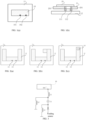
- some embodiments of the present embodiment provide an antenna assembly, as shown in FIGS. 1(a) and 1 (b) .
- the antenna assembly at least includes an antenna radiator 10, and a grounding point 101 and a feeding point 102 are arranged on the antenna radiator 10.
- the grounding point 101 is arranged on a middle portion of the antenna radiator 10.
- a same feeding source feeds an excitation signal into the antenna radiator 10 through the feeding point 102, so that the antenna radiator 10 supports a first frequency band and a second frequency band, and the first frequency band and the second frequency band are different from each other.
- the grounding point is arranged on the middle portion of the antenna radiator, and the use of a single-feed allows the antenna radiator to support different first and second frequency bands, achieving dual frequency radiation, and effectively expanding the working bandwidth of the antenna, i.e., increasing radiation bandwidth of the antenna, thereby improving antenna efficiency.
- the antenna radiator 10 is fed through the feeding point 102, and under the excitation of the feeding source, the antenna radiator 10 generates two different modes of resonances. That is, resonances of two different modes respectively corresponding to the first frequency band and the second frequency band are generated on the antenna radiator 10.
- the two different modes include a monopole antenna mode and a dipole antenna mode.
- the monopole antenna mode is configured to support the first frequency band
- the dipole antenna mode is configured to support the second frequency band.
- the first frequency band is lower than the second frequency band.
- the feeding point 102 is configured to be electrically connected to the feeding source, so that a signal generated by the feeding source may be transmitted to the antenna radiator 10 through the feeding point 102 and transmitted to the outside through the antenna radiator 10, or an external signal received by the antenna radiator 10 may be transmitted to the feeding source through the feeding point 102.
- the feeding source may include but is not limited to a signal in an Ultra Wide Band (UWB) frequency band.
- UWB Ultra Wide Band
- an excitation signal in the UWB frequency band is fed into the antenna radiator 10 through the feeding point 102, a resonance of the monopole antenna mode and a resonance of the dipole antenna mode in the UWB frequency band may be simultaneously generated on the antenna radiator 10. That is, both the monopole antenna mode and the dipole antenna mode in the UWB frequency band are simultaneously excited, thereby achieving dual-frequency radiation, increasing radiation bandwidth, and improving antenna efficiency.
- the feeding point 102 may be electrically connected to the feeding source through an elastic sheet 112.
- the feeding source may be arranged on a printed circuit board (PCB) 12 and electrically connected to the antenna radiator 10 at the feed point 102 through the elastic sheet 112.
- the elastic sheet 112 may be coupled to the antenna radiator 10 at the feeding point 102, or may be directly electrically connected to the antenna radiator 10 at the feeding point 102 through a metal through-hole 201.
- the grounding point 101 may be grounded through metal through-hole 201 and the elastic sheet 111.
- the grounding point 101 on the antenna radiator 10 may be electrically connected to a ground system of an electronic device through an elastic sheet 111, and the structure of the grounding point 101 may refer to the implementation of the feeding point and the feeding source, which is not repeated here.
- the ground system may be a metal frame or PCB ground board in the electronic device.
- the form of the ground system includes but is not limited to a metal conductive plate, or a metal conductive layer formed inside a flexible circuit board or a hard circuit board, etc.
- the antenna assembly provided by some embodiments of the present disclosure may further include an antenna bracket 11, and the antenna radiator 10 may be arranged on the antenna bracket 11 to form a bracket antenna.
- the antenna radiator 10 may be arranged on the antenna bracket 11 through laser-direct-structuring (LDS), or laser reconstructed print (LRP), etc.
- the antenna radiator 10 may be arranged on a PCB surface of the electronic device where the antenna assembly is located, and the antenna radiator 10 is a metal radiation patch to form a patch antenna.
- the antenna radiator 10 may be in a shape of a rectangle as shown in FIG. 1 (a) .
- the middle portion of the antenna radiator 10 may be a center point at a long side of the rectangle. That is, the grounding point 101 on the antenna radiator 10 is located at the center point of the long side of the rectangle.
- the center point here is not an absolute position, in which an error is allowed.
- FIG. 1 (a) just illustrates an example, and the grounding point 101 may be arranged adjacent to a center point at the other long side of the rectangle.
- the feeding point 101 and the grounding point 101 are arranged at the same side of the rectangle, positions of which are not limited, as long as resonances of two different modes in the same frequency band may be generated on the antenna radiator 10, that is, dual-frequency radiation may be achieved, when the feeding source feeds.
- the antenna radiator 10 is a patch antenna configured to be fed directly. When the patch antenna to be fed directly is served as a radiator, a wide impedance bandwidth in the UWB frequency band may be achieved, an excellent radiation performance is achieved, the size of the antenna assembly in the thickness direction is reduced, and the thickness of the electronic device is reduced.
- the antenna radiator 10 may be in a shape of a rectangle as shown in FIG. 1 (a) , a "U" shape as shown in FIGS. 2 (a) and 2 (c) , a zigzag shape as shown in FIG. 2 (b) , or an arc shape, which is not limited and may be adjusted according to actual design or production need.
- the shape of the antenna radiator 10 shown in FIG. 1 (a) is only an example and is not intended to limit the scope of protection of the present disclosure.
- the antenna radiator 10 may be in a "U" shape as shown in FIG. 2 (a) , and the "U" shape has the same length at the two sides (as shown in FIG. 2 (a) ) or different lengths at the two sides (as shown in FIG. 2 (c) ).
- the shape of the antenna radiator 10 may be as shown in FIG. 2 (b) , in which a folding edge is folded from one side of the "U" shape to present a zigzag shape.
- FIG. 2 (b) in which a folding edge is folded from one side of the "U" shape to present a zigzag shape.
- a slot 103 or the like may be defined on the antenna radiator 10.
- An impedance is adjusted as the shape of the antenna radiator 10 is adjusted, i.e., branches included in the antenna radiator 10 are adjusted, and then the current distribution is adjusted.
- the antenna assembly of the present disclosure flexibly and simply achieves the dual frequency radiation, increases the radiation bandwidth, and thus improves the antenna efficiency.
- the impedance matching control circuit may include an impedance switching device and multiple different impedance matching circuits connected in parallel and connected to the impedance switching device. In this way, one of the multiple different impedance matching circuits may be switched through the impedance switching device to adjust the matching impedance of the antenna. That is to say, the impedance matching circuit of the antenna assembly in some embodiments of the present disclosure may have an adjustable impedance value. By adjusting the impedance value of the impedance matching circuit, a corresponding resonance point may be adjusted to change the resonance point of the antenna, so that the antenna may operate in multiple frequency bands with a wider range and switch among different frequency bands. It should be noted that, in order to save space, the simplest impedance matching circuit may be configured. There are many implementations for the impedance matching control circuit and the impedance matching circuits in the embodiments of the present disclosure, which are not intended to limit the scope of the present disclosure.
- the antenna radiator 10 in the case where the feeding source is electrically connected to the antenna radiator 10 at the feeding point 102 through the impedance matching circuit and the elastic sheet 112, the antenna radiator 10 may be made to have a smaller size. In other embodiments, when the size of the antenna radiator 10 is large enough, for example, the antenna radiator 10 is in a shape of a larger rectangle, a larger "U" shape, or a larger zigzag shape, etc., the impedance matching circuits may not be configured.
- the length of the antenna radiator 10 may be 8mm
- the width of the antenna radiator 10 may be 2mm
- the grounding point 101 may be located at the center of the long side of the antenna radiator 10
- a distance between the feeding point 102 and the grounding point 101 may be 2mm (as shown in FIG. 1 (a) , the feeding point 102 arranged at the right side of the grounding point 101 is taken as an example)
- the thickness of the antenna bracket 11 may be 1mm
- the distance between the antenna bracket 11 and the PCB ground board 12 may be 1.5mm.
- the impedance matching circuit is shown in FIG.
- inductor L1 and a capacitor C1 are connected in series between the feed point 102 and the feeding source, one end of an inductor L2 is electrically connected to a connection point between the inductor L1 and the capacitor C1, the other end of inductor L2 is grounded, one end of an inductor L3 is electrically connected to the feeding source, and the other end of the inductor L3 is grounded.
- inductances of the inductor L1 and the inductor L3 may be 2nH
- an inductance of the inductor L2 may be 2.5nH
- a capacitance of the capacitor C1 may be 0.2PF.
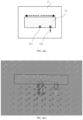
- the antenna assembly When the feeding source feeds a signal in the UWB frequency band, the antenna assembly provided in some embodiments of the present disclosure is a UWB antenna, and may excite two different modes. As shown in FIGS. 4 (a) and 4 (b) , currents of 6.5GHz on the antenna radiator 10 are in reversed directions, which corresponds to the monopole antenna mode. As shown in FIG. 5 (a) and FIG. 5 (b) , currents of 8GHz on antenna radiator 10 are in the same direction, which corresponds to the dipole antenna mode.
- FIG. 6 is a schematic diagram of a S11 curve of the antenna assembly served as the UWB antenna, it may be seen that, by referring to the S11 curve, when the feeding source feeds, the antenna assembly may generate two resonances.
- the resonance point of the first resonance may be located at 6.5GHz, and the resonance point of the second resonance may be located at 8GHz. From the schematic diagram of the S11 curve shown in FIG. 6 , it may be seen that return losses of the UWB antenna in some embodiments of the present embodiment may be less than -10dB at both monopole antenna mode and dipole antenna mode, in which minimum -20dB may reached. Moreover, both frequency bands at 6.5GHz and 8GHz meet the requirement of a bandwidth of 500MHz and have wideband characteristics. A Smith chart of the antenna assembly served as the UWB antenna in some embodiments of the present embodiment is shown in FIG. 7 . Therefore, the antenna assembly provided in some embodiments of the present disclosure achieves the dual frequency radiation, effectively expands the operating bandwidth of the antenna, that is, increases the radiation bandwidth, thereby improving the antenna efficiency.
- the operating frequency band of the antenna assembly provided in the embodiments of the present disclosure meets the coverage of at least 500MHz bandwidth in the range of 3.1GHz-10.6GHz.
- the operating frequency range of UWB antenna is from 3.1GHz to 10.6GHz, and the minimum operating bandwidth is 500MHz, which means the bandwidth of more than 500MHz is occupied in the 3.1GHz-10.6GHz frequency band. Therefore, the antenna assembly provided in the embodiments of the present disclosure may serve as the UWB antenna.
- the UWB is a short distance wireless communication technology, of which a transmission distance is less than 10m, and which adopts a bandwidth of more than 1GHz.
- the UWB does not adopts a carrier wave, but adopts non-sinusoidal narrow pulses in nanoseconds to picoseconds level to transmit data. Therefore, the UWB occupies a wide spectrum range, and is suitable for wireless personal communication with high speed and short distance.
- the antenna radiator 10 is larger than the antenna radiator 10 shown in FIG. 1 (a) .
- the antenna assembly provided in some embodiments of the present disclosure may effectively excite dual-frequency resonance even without the impedance matching circuit.
- the feeding source feeds a signal in the UWB frequency band
- two different modes are excited.
- currents of 6.5GHz on the antenna radiator 10 are in reversed directions, which corresponds to the monopole antenna mode.
- currents of 8GHz on antenna radiator 10 are in the same direction, which corresponds to the dipole antenna mode.
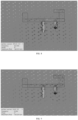
- FIG. 8 currents of 6.5GHz on the antenna radiator 10 are in reversed directions, which corresponds to the monopole antenna mode.
- FIG. 9 currents of 8GHz on antenna radiator 10 are in the same direction, which corresponds to the dipole antenna mode.
- FIG. 10 is a schematic diagram of a S11 curve of the antenna assembly served as the UWB antenna, it may be seen that, by referring to the S 1 1 curve, when the feeding source feeds, the antenna assembly may generate two resonances.
- the resonance point of the first resonance may be located at 6.5GHz
- the resonance point of the second resonance may be located at 8GHz. Both 6.5GHz and 8GHz frequency bands meet the requirement of a bandwidth of 500MHz and have wideband characteristics.
- a Smith chart of the antenna assembly served as the UWB antenna in some embodiments of the present embodiment is shown in FIG. 11 . Therefore, the antenna assembly provided in some embodiments of the present disclosure achieves the dual frequency radiation, effectively expands the working bandwidth of the antenna, that is, increase the radiation bandwidth, thereby improving the antenna efficiency.
- Some embodiments of the present disclosure provide a dual-frequency wideband antenna including an antenna assembly, the antenna assembly includes the antenna radiator 10, and the grounding point 101 and the feeding point 102 are arranged on the antenna radiator 10.
- the grounding point 101 is arranged on the middle portion of the antenna radiator 10.
- the excitation signals are fed into the antenna radiator 10 through the feeding point 102, resonances of two different modes in the UWB frequency band are generated on the antenna radiator 10, and the resonances of two different modes of the dual-frequency wideband antenna may include the resonance in the monopole antenna mode and the resonance in the dipole antenna mode.
- the antenna assembly provided in some embodiments of the present disclosure may include the antenna bracket 11, and the antenna radiator 10 may be arranged on the antenna bracket 11 to form the bracket antenna.
- the antenna radiator 10 may be arranged on the PCB surface of the electronic device where the antenna assembly is located to form a patch antenna.
- the dual-frequency wideband antenna may include the impedance matching circuit arranged between the feeding source and the feeding point 102.
- the antenna radiator 10 may in a shape of a rectangle, and the grounding point 101 on the antenna radiator 10 is located at the center point of the long side of the rectangle.
- the length of the antenna radiator 10 may be 8mm
- the width of the antenna radiator 10 may be 2mm
- the distance between the feeding point 102 and the grounding point 101 on antenna radiator 10 may be 2mm
- the thickness of antenna bracket 11 in the dual-frequency wideband antenna may be 1mm
- the distance between the antenna bracket 11 and the ground board of the electronic device where the dual-frequency wideband antenna is located is 1.5mm.
- the ground board may include the middle frame or PCB ground board of the electronic device where the dual-frequency wideband antenna is located.
- the antenna may be called a low profile antenna (LPA).
- LPA low profile antenna
- the dual-frequency wideband antenna provided in some embodiments of the present disclosure since the distance between the antenna bracket 11 carrying the antenna radiator 10 and the ground board of the electronic device where the dual-frequency wideband antenna is located is only 1.5mm, which is far less than 0.1 times the wavelength of 37.5mm corresponding to 8GHz, the dual-frequency wideband antenna provided in some embodiments of the present disclosure is the low profile antenna, thereby effectively meeting the lightweight requirement for the electronic device where the dual-frequency wideband antenna is located.
- the dual-frequency wideband antenna provided in some embodiments of the present disclosure may further has single-feed wideband dual-frequency characteristics. As shown in FIG.
- the dual-frequency wideband antenna provided in some embodiments of the present disclosure is a low profile dual-frequency wideband antenna, which ensures the minimization of antenna size and maximizes the coverage of the frequency range of the antenna, thereby improving the antenna efficiency.
- the dual-frequency wideband antenna provided in some embodiments of the present disclosure effectively meets UWB positioning requirement, covers resonant frequency bands of two different modes.
- the frequency bands of 6.5GHz and 8GHz are covered, so that good resonance is achieved, bandwidth is expanded, and the dual-frequency wideband antenna has a small size.
- the dual-frequency wideband antenna provided in the embodiments of the present disclosure is the low profile dual-frequency wideband antenna, which ensures the minimization of antenna size and achieves maximum frequency coverage, thereby improving the antenna efficiency.
- Some embodiments of the present disclosure provide an electronic device including the dual-frequency wideband antenna as described in any one of the embodiments of the present disclosure.
- the electronic device provided in the embodiments of the present disclosure may be any device with communication functions, such as a tablet, a mobile phone, an e-reader, a remote control, a personal computer, a laptop, a car device, a network TV, a wearable device, or other devices.
- the electronic device may achieve an electromagnetic wave communication function, that is, the electronic device may receive and/or transmit electromagnetic wave signals.
Landscapes
- Engineering & Computer Science (AREA)
- Computer Networks & Wireless Communication (AREA)
- Details Of Aerials (AREA)
- Support Of Aerials (AREA)
Abstract
Description
- The present disclosure relates to the field of wireless communication technology, in particular to an antenna assembly, a dual-frequency wideband antenna, and an electronic device.
- In recent years, mobile communication has become increasingly important in people's lives. In the era of the fifth generation (5G) mobile communication system, the requirements for antennas are increasingly raised.
- Since an electronic device has a small space for antennas, how to ensure a small size and great radiation bandwidth of the antennas at the same time is an urgent problem.
- Embodiments of the present disclosure provide an antenna assembly, a dual-frequency wideband antenna, and an electronic device, which increase radiation bandwidth and improve antenna efficiency.
- Some embodiments of the present disclosure provide an antenna assembly including an antenna radiator. A grounding point and a feeding point are arranged on the antenna radiator, and the grounding point is arranged on a middle portion of the antenna radiator. A same feeding source feeds an excitation signal into the antenna radiator through the feeding point to enable the antenna radiator to support a first frequency band and a second frequency band, and the first frequency band is different from the second frequency band.
- In the antenna assembly in some embodiments of the present disclosure, the grounding point is arranged on the middle portion of the antenna radiator, and the use of a single-feed allows the antenna radiator to support different first and second frequency bands, achieving dual frequency radiation, and effectively expanding working bandwidth of the antenna, that is, increasing radiation bandwidth of the antenna, thereby improving antenna efficiency.
- Some embodiments of the present disclosure provide a dual-frequency wideband antenna including an antenna assembly, the antenna assembly includes an antenna radiator, and a grounding point and a feeding point are arranged on the antenna radiator. The grounding point is arranged on a middle portion of the antenna radiator. The antenna radiator is fed into an excitation signal through the feeding point, two different modes of resonances is generated in an ultra wide band (UWB) frequency band on the antenna radiator, and the two different modes of resonances includes a resonance in a monopole antenna mode and a resonance in a dipole antenna mode.
- The dual-frequency wideband antenna provided in some embodiments of the present disclosure effectively meets the UWB positioning requirement, covers the two different modes of resonant frequency bands. In some embodiments, the frequency bands of 6.5GHz and 8GHz are covered, so that good resonance achieved, bandwidth is expanded, and the dual-frequency wideband antenna has a small size. In some embodiments, the dual-frequency wideband antenna provided in the embodiments of the present disclosure is the low profile dual-frequency wideband antenna, which ensures the minimization of antenna volume and achieves maximum frequency coverage, thereby improving the antenna efficiency.
- Some embodiments of the present disclosure provide an electronic device including any one of the dual-frequency wideband antenna mentioned above. The electronic device meets the UWB positioning requirement, covers the frequency bands of 6.5GHz and 8GHz, achieves good resonance, expands bandwidth, and has a small size.
- Other features and technical effects of the present disclosure will be described in the following specification, and a part of the other features and technical effects may become obvious from the specification, or may be learned by implementing the present disclosure. The purpose and other technical effects of the present disclosure may be achieved and obtained through the structures indicated in the specification, claims, and drawings.
- The drawings are used to further understand the technical solutions of the present disclosure, constitutes a part of the specification, are used together with embodiments of the present disclosure to explain the technical solutions of the present disclosure, and are not used to limit the technical solutions of the present disclosure.
-
FIG. 1 (a) is a top view structural schematic view of an antenna assembly according to a first embodiment of the of the present disclosure. -
FIG. 1 (b) is a side view structural schematic view of the antenna assembly according to the first embodiment of the of the present disclosure. -
FIG. 2 (a) is a structural schematic view of an antenna assembly according to a second embodiment of the of the present disclosure. -
FIG. 2 (b) is a structural schematic view of an antenna assembly according to a third embodiment of the of the present disclosure. -
FIG. 2 (c) is a structural schematic view of an antenna assembly according to a fourth embodiment of the of the present disclosure. -
FIG. 3 is a diagram of an impedance matching circuit according to some embodiments of the of the present disclosure. -
FIG. 4 (a) is a schematic diagram of a current distribution of an antenna assembly served as an UWB antenna at a resonant frequency of 6.5GHz according to a first embodiment of the of the present disclosure. -
FIG. 4 (b) is a schematic diagram of a simulation current distribution of the antenna assembly served as the UWB antenna at the resonant frequency of 6.5GHz according to the first embodiment of the present disclosure. -
FIG. 5 (a) is a schematic diagram of the current distribution of the antenna assembly served as the UWB antenna at a resonant frequency of 8GHz according to the first embodiment of the present disclosure. -
FIG. 5 (b) is a schematic diagram of a simulation current distribution of the antenna assembly served as the UWB antenna at the resonant frequency of 8GHz according to the first embodiment of the present disclosure. -
FIG. 6 is a schematic diagram of a S11 curve of the antenna assembly served as the UWB antenna according to the first embodiment of the present disclosure. -
FIG. 7 is a Smith chart of the antenna assembly served as the UWB antenna according to the first embodiment of the present disclosure. -
FIG. 8 is a schematic diagram of a simulation current distribution of an antenna assembly served as an UWB antenna at a resonant frequency of 6.5GHz according to a second embodiment of the present disclosure. -
FIG. 9 is a schematic diagram of a simulation current distribution of the antenna assembly served as the UWB antenna at a resonant frequency of 8GHz according to the second embodiment of the present disclosure. -
FIG. 10 is a schematic diagram of a S11 curve of the antenna assembly served as the UWB antenna according to the second embodiment of the present disclosure. -
FIG. 11 is a Smith chart of the antenna assembly served as the UWB antenna according to the second embodiment of the present disclosure. - In order to clarify the purpose, technical solutions, and technical effects of the present disclosure, embodiments of the present disclosure are detailly described in conjunction with the drawings. It should be noted that, in the absence of conflicts, embodiments and features in the embodiments of the present disclosure may be combined arbitrarily with each other.
- In order to facilitate understanding of the present disclosure, a comprehensive description of the present disclosure is provided in conjunction with relevant drawings. The embodiments of the present disclosure are shown in the accompanying drawings. However, the present disclosure may be implemented in many different forms and is not limited to the embodiments described herein. The purpose of the embodiments is to make the present disclosure clear and comprehensive.
- Unless otherwise defined, all technical and scientific terms used in the embodiments of the present disclosure have the same meanings as understood by those skilled in the art. The terms used in the specification of the present disclosure are only for the purpose of describing embodiments and are not intended to limit the scope of the present disclosure.
- It should be understood that terms "first" and "second" in embodiments of the present disclosure are only used for description purposes and cannot be understood as indicating or implying relative importance or implicitly indicating the number of technical features indicated. Thus, features defined as "first" and "second" may explicitly or implicitly include at least one of the features. In the embodiments of the present disclosure, "multiple" means at least two, such as two, or three, etc., unless otherwise specifically defined.
- It should be understood that, in the following embodiments, the term "connection" should be understood as "electrical connection" or "communication connection", etc. if there are transmission of electrical signals or data between the connected circuits, modules, or units, etc.
- When used, singular forms of "a" and "the" may include plural forms, unless the context clearly indicates otherwise. It should be understood that the terms "include/contain" or "have" represent the existence of the stated features, whole, step, operation, assembly, part, or combinations thereof, but do not exclude the possibility of the existence or addition of one or more other features, whole, step, operation, assembly, part, or combinations thereof. In addition, the term "and/or" used in the specification includes any and all combinations of the listed items.
- In order to increase a radiation bandwidth of an antenna and improve antenna efficiency, some embodiments of the present embodiment provide an antenna assembly, as shown in
FIGS. 1(a) and1 (b) . The antenna assembly at least includes anantenna radiator 10, and agrounding point 101 and afeeding point 102 are arranged on theantenna radiator 10. - The
grounding point 101 is arranged on a middle portion of theantenna radiator 10. - A same feeding source feeds an excitation signal into the
antenna radiator 10 through thefeeding point 102, so that theantenna radiator 10 supports a first frequency band and a second frequency band, and the first frequency band and the second frequency band are different from each other. - In the antenna assembly in some embodiments of the present disclosure, the grounding point is arranged on the middle portion of the antenna radiator, and the use of a single-feed allows the antenna radiator to support different first and second frequency bands, achieving dual frequency radiation, and effectively expanding the working bandwidth of the antenna, i.e., increasing radiation bandwidth of the antenna, thereby improving antenna efficiency.
- In some embodiments, the
antenna radiator 10 is fed through thefeeding point 102, and under the excitation of the feeding source, theantenna radiator 10 generates two different modes of resonances. That is, resonances of two different modes respectively corresponding to the first frequency band and the second frequency band are generated on theantenna radiator 10. The two different modes include a monopole antenna mode and a dipole antenna mode. The monopole antenna mode is configured to support the first frequency band, and the dipole antenna mode is configured to support the second frequency band. In some embodiments, the first frequency band is lower than the second frequency band. - In some embodiments, the
feeding point 102 is configured to be electrically connected to the feeding source, so that a signal generated by the feeding source may be transmitted to theantenna radiator 10 through thefeeding point 102 and transmitted to the outside through theantenna radiator 10, or an external signal received by theantenna radiator 10 may be transmitted to the feeding source through thefeeding point 102. In some embodiments, the feeding source may include but is not limited to a signal in an Ultra Wide Band (UWB) frequency band. - In some embodiments, an excitation signal in the UWB frequency band is fed into the
antenna radiator 10 through thefeeding point 102, a resonance of the monopole antenna mode and a resonance of the dipole antenna mode in the UWB frequency band may be simultaneously generated on theantenna radiator 10. That is, both the monopole antenna mode and the dipole antenna mode in the UWB frequency band are simultaneously excited, thereby achieving dual-frequency radiation, increasing radiation bandwidth, and improving antenna efficiency. - In some embodiments, as shown in
FIG. 1 (b) , thefeeding point 102 may be electrically connected to the feeding source through anelastic sheet 112. In some embodiments, the feeding source may be arranged on a printed circuit board (PCB) 12 and electrically connected to theantenna radiator 10 at thefeed point 102 through theelastic sheet 112. Theelastic sheet 112 may be coupled to theantenna radiator 10 at thefeeding point 102, or may be directly electrically connected to theantenna radiator 10 at thefeeding point 102 through a metal through-hole 201. Thegrounding point 101 may be grounded through metal through-hole 201 and theelastic sheet 111. In some embodiments, thegrounding point 101 on theantenna radiator 10 may be electrically connected to a ground system of an electronic device through anelastic sheet 111, and the structure of thegrounding point 101 may refer to the implementation of the feeding point and the feeding source, which is not repeated here. It should be understood that, the ground system may be a metal frame or PCB ground board in the electronic device. In some embodiments, the form of the ground system includes but is not limited to a metal conductive plate, or a metal conductive layer formed inside a flexible circuit board or a hard circuit board, etc. - In some embodiments, as shown in
FIGS. 1 (a) and 1 (b) , the antenna assembly provided by some embodiments of the present disclosure may further include anantenna bracket 11, and theantenna radiator 10 may be arranged on theantenna bracket 11 to form a bracket antenna. In some embodiments, theantenna radiator 10 may be arranged on theantenna bracket 11 through laser-direct-structuring (LDS), or laser reconstructed print (LRP), etc. - In some embodiments, the
antenna radiator 10 may be arranged on a PCB surface of the electronic device where the antenna assembly is located, and theantenna radiator 10 is a metal radiation patch to form a patch antenna. - In some embodiments, the
antenna radiator 10 may be in a shape of a rectangle as shown inFIG. 1 (a) . In some embodiments, in order to generate resonances of two different modes better when the feeding source feeds and improve the radiation characteristics of the antenna structure, the middle portion of theantenna radiator 10 may be a center point at a long side of the rectangle. That is, thegrounding point 101 on theantenna radiator 10 is located at the center point of the long side of the rectangle. The center point here is not an absolute position, in which an error is allowed.FIG. 1 (a) just illustrates an example, and thegrounding point 101 may be arranged adjacent to a center point at the other long side of the rectangle. Thefeeding point 101 and thegrounding point 101 are arranged at the same side of the rectangle, positions of which are not limited, as long as resonances of two different modes in the same frequency band may be generated on theantenna radiator 10, that is, dual-frequency radiation may be achieved, when the feeding source feeds. In some embodiments, theantenna radiator 10 is a patch antenna configured to be fed directly. When the patch antenna to be fed directly is served as a radiator, a wide impedance bandwidth in the UWB frequency band may be achieved, an excellent radiation performance is achieved, the size of the antenna assembly in the thickness direction is reduced, and the thickness of the electronic device is reduced. - It should be noted that the
antenna radiator 10 may be in a shape of a rectangle as shown inFIG. 1 (a) , a "U" shape as shown inFIGS. 2 (a) and 2 (c) , a zigzag shape as shown inFIG. 2 (b) , or an arc shape, which is not limited and may be adjusted according to actual design or production need. - In some embodiments, the shape of the
antenna radiator 10 shown inFIG. 1 (a) is only an example and is not intended to limit the scope of protection of the present disclosure. In some embodiments, theantenna radiator 10 may be in a "U" shape as shown inFIG. 2 (a) , and the "U" shape has the same length at the two sides (as shown inFIG. 2 (a) ) or different lengths at the two sides (as shown inFIG. 2 (c) ). In another some embodiments, the shape of theantenna radiator 10 may be as shown inFIG. 2 (b) , in which a folding edge is folded from one side of the "U" shape to present a zigzag shape. In another some embodiments, as shown inFIG. 2 (c) , aslot 103 or the like may be defined on theantenna radiator 10. An impedance is adjusted as the shape of theantenna radiator 10 is adjusted, i.e., branches included in theantenna radiator 10 are adjusted, and then the current distribution is adjusted. Thus, the antenna assembly of the present disclosure flexibly and simply achieves the dual frequency radiation, increases the radiation bandwidth, and thus improves the antenna efficiency. - In some embodiments, the antenna assembly provided by the embodiments of the present disclosure may further include an impedance matching circuit, and the feeding source is electrically connected to the
feeding point 102 through the impedance matching circuit, so that an equivalent impedance of which theantenna radiator 10 as the antenna body is connected to the impedance matching circuit is matched with an input impedance of the feeding source, thereby improving the radiation efficiency of the antenna. In some embodiments, thefeeding point 102 is electrically connected to the impedance matching circuit through theelastic sheet 112. That is, the feeding source may be electrically connected to theantenna radiator 10 at thefeeding point 102 through the impedance matching circuit and theelastic sheet 112. In some embodiments, the antenna assembly may include an impedance matching control circuit configured to select from multiple impedance matching circuits. The impedance matching control circuit may include an impedance switching device and multiple different impedance matching circuits connected in parallel and connected to the impedance switching device. In this way, one of the multiple different impedance matching circuits may be switched through the impedance switching device to adjust the matching impedance of the antenna. That is to say, the impedance matching circuit of the antenna assembly in some embodiments of the present disclosure may have an adjustable impedance value. By adjusting the impedance value of the impedance matching circuit, a corresponding resonance point may be adjusted to change the resonance point of the antenna, so that the antenna may operate in multiple frequency bands with a wider range and switch among different frequency bands. It should be noted that, in order to save space, the simplest impedance matching circuit may be configured. There are many implementations for the impedance matching control circuit and the impedance matching circuits in the embodiments of the present disclosure, which are not intended to limit the scope of the present disclosure. - In some embodiments, in the case where the feeding source is electrically connected to the
antenna radiator 10 at thefeeding point 102 through the impedance matching circuit and theelastic sheet 112, theantenna radiator 10 may be made to have a smaller size. In other embodiments, when the size of theantenna radiator 10 is large enough, for example, theantenna radiator 10 is in a shape of a larger rectangle, a larger "U" shape, or a larger zigzag shape, etc., the impedance matching circuits may not be configured. - For example, in the antenna assembly shown in
FIG. 1 (a) , the length of theantenna radiator 10 may be 8mm, the width of theantenna radiator 10 may be 2mm, thegrounding point 101 may be located at the center of the long side of theantenna radiator 10, a distance between thefeeding point 102 and thegrounding point 101 may be 2mm (as shown inFIG. 1 (a) , thefeeding point 102 arranged at the right side of thegrounding point 101 is taken as an example), the thickness of theantenna bracket 11 may be 1mm, and the distance between theantenna bracket 11 and thePCB ground board 12 may be 1.5mm. In some embodiments, the impedance matching circuit is shown inFIG. 3 , in which an inductor L1 and a capacitor C1 are connected in series between thefeed point 102 and the feeding source, one end of an inductor L2 is electrically connected to a connection point between the inductor L1 and the capacitor C1, the other end of inductor L2 is grounded, one end of an inductor L3 is electrically connected to the feeding source, and the other end of the inductor L3 is grounded. In some embodiments, inductances of the inductor L1 and the inductor L3 may be 2nH, an inductance of the inductor L2 may be 2.5nH, and a capacitance of the capacitor C1 may be 0.2PF. It should be noted that there are many implementations for the impedance matching circuit in the embodiments of the present disclosure. The impedance matching circuit shown inFIG. 3 is only an example and is not intended to limit the scope of the present disclosure. - When the feeding source feeds a signal in the UWB frequency band, the antenna assembly provided in some embodiments of the present disclosure is a UWB antenna, and may excite two different modes. As shown in
FIGS. 4 (a) and 4 (b) , currents of 6.5GHz on theantenna radiator 10 are in reversed directions, which corresponds to the monopole antenna mode. As shown inFIG. 5 (a) and FIG. 5 (b) , currents of 8GHz onantenna radiator 10 are in the same direction, which corresponds to the dipole antenna mode.FIG. 6 is a schematic diagram of a S11 curve of the antenna assembly served as the UWB antenna, it may be seen that, by referring to the S11 curve, when the feeding source feeds, the antenna assembly may generate two resonances. The resonance point of the first resonance may be located at 6.5GHz, and the resonance point of the second resonance may be located at 8GHz. From the schematic diagram of the S11 curve shown inFIG. 6 , it may be seen that return losses of the UWB antenna in some embodiments of the present embodiment may be less than -10dB at both monopole antenna mode and dipole antenna mode, in which minimum -20dB may reached. Moreover, both frequency bands at 6.5GHz and 8GHz meet the requirement of a bandwidth of 500MHz and have wideband characteristics. A Smith chart of the antenna assembly served as the UWB antenna in some embodiments of the present embodiment is shown inFIG. 7 . Therefore, the antenna assembly provided in some embodiments of the present disclosure achieves the dual frequency radiation, effectively expands the operating bandwidth of the antenna, that is, increases the radiation bandwidth, thereby improving the antenna efficiency. - The operating frequency band of the antenna assembly provided in the embodiments of the present disclosure meets the coverage of at least 500MHz bandwidth in the range of 3.1GHz-10.6GHz. According to the regulations of the Federal Communications Commission (FCC) in the United States, the operating frequency range of UWB antenna is from 3.1GHz to 10.6GHz, and the minimum operating bandwidth is 500MHz, which means the bandwidth of more than 500MHz is occupied in the 3.1GHz-10.6GHz frequency band. Therefore, the antenna assembly provided in the embodiments of the present disclosure may serve as the UWB antenna. The UWB is a short distance wireless communication technology, of which a transmission distance is less than 10m, and which adopts a bandwidth of more than 1GHz. The UWB does not adopts a carrier wave, but adopts non-sinusoidal narrow pulses in nanoseconds to picoseconds level to transmit data. Therefore, the UWB occupies a wide spectrum range, and is suitable for wireless personal communication with high speed and short distance.
- For another example, as shown in
FIG. 2 (b) , in this embodiment, theantenna radiator 10 is larger than theantenna radiator 10 shown inFIG. 1 (a) . In the case where theantenna radiator 10 is increased, the antenna assembly provided in some embodiments of the present disclosure may effectively excite dual-frequency resonance even without the impedance matching circuit. When the feeding source feeds a signal in the UWB frequency band, two different modes are excited. As shown inFIG. 8 , currents of 6.5GHz on theantenna radiator 10 are in reversed directions, which corresponds to the monopole antenna mode. As shown inFIG. 9 , currents of 8GHz onantenna radiator 10 are in the same direction, which corresponds to the dipole antenna mode.FIG. 10 is a schematic diagram of a S11 curve of the antenna assembly served as the UWB antenna, it may be seen that, by referring to theS 1 1 curve, when the feeding source feeds, the antenna assembly may generate two resonances. The resonance point of the first resonance may be located at 6.5GHz, and the resonance point of the second resonance may be located at 8GHz. Both 6.5GHz and 8GHz frequency bands meet the requirement of a bandwidth of 500MHz and have wideband characteristics. A Smith chart of the antenna assembly served as the UWB antenna in some embodiments of the present embodiment is shown inFIG. 11 . Therefore, the antenna assembly provided in some embodiments of the present disclosure achieves the dual frequency radiation, effectively expands the working bandwidth of the antenna, that is, increase the radiation bandwidth, thereby improving the antenna efficiency. - Some embodiments of the present disclosure provide a dual-frequency wideband antenna including an antenna assembly, the antenna assembly includes the
antenna radiator 10, and thegrounding point 101 and thefeeding point 102 are arranged on theantenna radiator 10. - The
grounding point 101 is arranged on the middle portion of theantenna radiator 10. - The excitation signals are fed into the
antenna radiator 10 through thefeeding point 102, resonances of two different modes in the UWB frequency band are generated on theantenna radiator 10, and the resonances of two different modes of the dual-frequency wideband antenna may include the resonance in the monopole antenna mode and the resonance in the dipole antenna mode. - In some embodiments, the antenna assembly provided in some embodiments of the present disclosure may include the
antenna bracket 11, and theantenna radiator 10 may be arranged on theantenna bracket 11 to form the bracket antenna. - In some embodiments, the
antenna radiator 10 may be arranged on the PCB surface of the electronic device where the antenna assembly is located to form a patch antenna. - In some embodiment, the dual-frequency wideband antenna provided in some embodiments of the present disclosure may include the impedance matching circuit arranged between the feeding source and the
feeding point 102. In some embodiments, theantenna radiator 10 may in a shape of a rectangle, and thegrounding point 101 on theantenna radiator 10 is located at the center point of the long side of the rectangle. In some embodiments, the length of theantenna radiator 10 may be 8mm, the width of theantenna radiator 10 may be 2mm, the distance between thefeeding point 102 and thegrounding point 101 onantenna radiator 10 may be 2mm, the thickness ofantenna bracket 11 in the dual-frequency wideband antenna may be 1mm, and the distance between theantenna bracket 11 and the ground board of the electronic device where the dual-frequency wideband antenna is located is 1.5mm. In some embodiments, the ground board may include the middle frame or PCB ground board of the electronic device where the dual-frequency wideband antenna is located. - Generally speaking, for an antenna with an overall height less than 0.1 times the wavelength, the antenna may be called a low profile antenna (LPA). In the dual-frequency wideband antenna provided in some embodiments of the present disclosure, since the distance between the
antenna bracket 11 carrying theantenna radiator 10 and the ground board of the electronic device where the dual-frequency wideband antenna is located is only 1.5mm, which is far less than 0.1 times the wavelength of 37.5mm corresponding to 8GHz, the dual-frequency wideband antenna provided in some embodiments of the present disclosure is the low profile antenna, thereby effectively meeting the lightweight requirement for the electronic device where the dual-frequency wideband antenna is located. Moreover, the dual-frequency wideband antenna provided in some embodiments of the present disclosure may further has single-feed wideband dual-frequency characteristics. As shown inFIG. 6 ,UWB channels - The dual-frequency wideband antenna provided in some embodiments of the present disclosure effectively meets UWB positioning requirement, covers resonant frequency bands of two different modes. In some embodiments, the frequency bands of 6.5GHz and 8GHz are covered, so that good resonance is achieved, bandwidth is expanded, and the dual-frequency wideband antenna has a small size. In some embodiments, the dual-frequency wideband antenna provided in the embodiments of the present disclosure is the low profile dual-frequency wideband antenna, which ensures the minimization of antenna size and achieves maximum frequency coverage, thereby improving the antenna efficiency.
- Some embodiments of the present disclosure provide an electronic device including the dual-frequency wideband antenna as described in any one of the embodiments of the present disclosure. The electronic device provided in the embodiments of the present disclosure may be any device with communication functions, such as a tablet, a mobile phone, an e-reader, a remote control, a personal computer, a laptop, a car device, a network TV, a wearable device, or other devices. The electronic device may achieve an electromagnetic wave communication function, that is, the electronic device may receive and/or transmit electromagnetic wave signals.
- Although the embodiments disclosed in the present disclosure are as described above, the content is only for the convenience of understanding the embodiments adopted in the present disclosure and is not intended to limit the present disclosure. Those skilled in the art may make any modifications and changes in the form and details of the implementation without departing from the spirit and scope disclosed in the present disclosure, but the scope the present disclosure shall still be subject to the scope defined in the appended claims.
Claims (19)
- An antenna assembly, comprising an antenna radiator; and a grounding point and a feeding point being arranged on the antenna radiator;wherein the grounding point is arranged on a middle portion of the antenna radiator;a same feeding source feeds an excitation signal into the antenna radiator through the feeding point to enable the antenna radiator to support a first frequency band and a second frequency band, and the first frequency band is different from the second frequency band.
- The antenna assembly as claimed in claim 1, wherein the antenna radiator generates a monopole antenna mode and a dipole antenna mode under the excitation of the feeding source;
the monopole antenna mode is configured to support the first frequency band, and the dipole antenna mode is configured to support the second frequency band. - The antenna assembly as claimed in claim 1, further comprising an impedance matching circuit;
wherein the feeding source is electrically connected to the feeding point through the impedance matching circuit. - The antenna assembly as claimed in claim 1 or 3, wherein the feeding point is electrically connected to the feeding source or the impedance matching circuit through an elastic sheet, the grounding point is grounded through an elastic sheet.
- The antenna assembly as claimed in claim 3, wherein the impedance matching circuit comprises an inductor L1, a capacitor C1, an inductor L2, and an inductor L3;the inductor L1 and the capacitor C1 are connected in series between the feeding point and the feeding source;one end of the inductor L2 is electrically connected to a connection point between the inductor L1 and the capacitor C1, and the other end of the inductor L2 is grounded;one end of the inductor L3 is electrically connected to the feeding source, and the other end of the inductor L3 is grounded.
- The antenna assembly as claimed in claim 1, further comprising:
an antenna bracket; wherein the antenna radiator is arranged on the antenna bracket. - The antenna assembly as claimed in claim 6, wherein the antenna radiator is arranged on the antenna bracket through laser-direct-structuring (LDS) or laser reconstructed print (LRP) technology.
- The antenna assembly as claimed in claim 1, wherein the antenna radiator is arranged on a printed circuit board (PCB) of an electronic device where the antenna assembly is located, and the antenna radiator is a metal radiation patch.
- The antenna assembly as claimed in claim 1 or 3, wherein a slot is defined on the antenna radiator.
- The antenna assembly as claimed in claim 1 or 3, wherein the antenna radiator is in a shape of a rectangle, a "U", a zigzag, or an arc.
- The antenna assembly as claimed in claim 10, wherein the antenna radiator is in the shape of the rectangle, and the middle portion is a center point of a long side of the rectangle.
- A dual-frequency wideband antenna, comprising an antenna assembly, the antenna assembly comprising an antenna radiator, and a grounding point and a feeding point being arranged on the antenna radiator;wherein the grounding point is arranged on a middle portion of the antenna radiator;the antenna radiator is fed into an excitation signal through the feeding point, resonances of two different modes in an ultra wide band (UWB) frequency band are generated on the antenna radiator, and the resonances of two different modes comprises a resonance of a monopole antenna mode and a resonance of a dipole antenna mode.
- The antenna assembly as claimed in claim 12, comprising an antenna bracket; wherein the antenna radiator is arranged on the antenna bracket.
- The antenna assembly as claimed in claim 13, wherein the antenna radiator is arranged on the antenna bracket through laser-direct-structuring (LDS) or laser reconstructed print (LRP) technology.
- The antenna assembly as claimed in claim 12, wherein the antenna radiator is arranged on a printed circuit board (PCB) of an electronic device where the antenna assembly is located, and the antenna radiator is a metal radiation patch.
- The dual-frequency wideband antenna according to claim 12, further comprising an impedance matching circuit arranged between the feeding source and the feeding point;wherein the antenna radiator is in a shape of a rectangle, and the grounding point is located at a center point of a long side of the rectangle;a length of the antenna radiator is 8mm, a width of the antenna radiator is 2mm, a distance between the feeding point and the grounding point is 2mm, a thickness of the antenna bracket is 1mm, and a distance between the antenna bracket and a ground board of the electronic device where the dual-frequency wideband antenna is located is 1.5mm.
- The dual-frequency wideband antenna according to claim 16, wherein the impedance matching circuit comprises an inductor L1, a capacitor C1, an inductor L2, and an inductor L3;the inductor L1 and the capacitor C1 are connected in series between the feeding point and the feeding source;one end of the inductor L2 is electrically connected to a connection point between the inductor L1 and the capacitor C1, and the other end of the inductor L2 is grounded;one end of the inductor L3 is electrically connected to the feeding source, and the other end of the inductor L3 is grounded.
- The dual-frequency wideband antenna as claimed in claims 12, 13, or 16, wherein the antenna radiator is in a shape of a rectangle, a "U", a zigzag, or an arc.
- An electronic device, comprising a dual-frequency wideband antenna as claimed in any one of claims 12-18.
Applications Claiming Priority (2)
| Application Number | Priority Date | Filing Date | Title |
|---|---|---|---|
| CN202210234322.7A CN116780162A (en) | 2022-03-10 | 2022-03-10 | Antenna assemblies, dual-band broadband antennas and electronic equipment |
| PCT/CN2022/140156 WO2023169040A1 (en) | 2022-03-10 | 2022-12-19 | Antenna assembly, dual-frequency wideband antenna, and electronic device |
Publications (2)
| Publication Number | Publication Date |
|---|---|
| EP4489218A1 true EP4489218A1 (en) | 2025-01-08 |
| EP4489218A4 EP4489218A4 (en) | 2025-06-11 |
Family
ID=87937172
Family Applications (1)
| Application Number | Title | Priority Date | Filing Date |
|---|---|---|---|
| EP22930660.0A Pending EP4489218A4 (en) | 2022-03-10 | 2022-12-19 | Antenna assembly, dual-frequency wideband antenna, and electronic device |
Country Status (4)
| Country | Link |
|---|---|
| US (1) | US20240429603A1 (en) |
| EP (1) | EP4489218A4 (en) |
| CN (1) | CN116780162A (en) |
| WO (1) | WO2023169040A1 (en) |
Family Cites Families (9)
| Publication number | Priority date | Publication date | Assignee | Title |
|---|---|---|---|---|
| US7834813B2 (en) * | 2004-10-15 | 2010-11-16 | Skycross, Inc. | Methods and apparatuses for adaptively controlling antenna parameters to enhance efficiency and maintain antenna size compactness |
| CN101102008B (en) * | 2006-07-04 | 2012-02-08 | 富士康(昆山)电脑接插件有限公司 | multi-frequency antenna |
| TWI419405B (en) * | 2009-10-08 | 2013-12-11 | Acer Inc | Mobile communication device and its antenna |
| CN203367469U (en) * | 2013-07-05 | 2013-12-25 | 上海安费诺永亿通讯电子有限公司 | Broadband antenna applied to wireless electronic product |
| CN105337040B (en) * | 2014-07-07 | 2019-03-08 | 联想(北京)有限公司 | Antenna assembly and electronic equipment |
| US10084241B1 (en) * | 2018-02-23 | 2018-09-25 | Qualcomm Incorporated | Dual-polarization antenna system |
| JP6729843B1 (en) * | 2019-05-27 | 2020-07-29 | 株式会社村田製作所 | RFID tag |
| US10957978B2 (en) * | 2019-06-28 | 2021-03-23 | Apple Inc. | Electronic devices having multi-frequency ultra-wideband antennas |
| CN114122685B (en) * | 2020-08-31 | 2025-09-30 | 华为技术有限公司 | Antenna unit and electronics |
-
2022
- 2022-03-10 CN CN202210234322.7A patent/CN116780162A/en active Pending
- 2022-12-19 EP EP22930660.0A patent/EP4489218A4/en active Pending
- 2022-12-19 WO PCT/CN2022/140156 patent/WO2023169040A1/en not_active Ceased
-
2024
- 2024-08-27 US US18/817,088 patent/US20240429603A1/en active Pending
Also Published As
| Publication number | Publication date |
|---|---|
| US20240429603A1 (en) | 2024-12-26 |
| CN116780162A (en) | 2023-09-19 |
| WO2023169040A1 (en) | 2023-09-14 |
| EP4489218A4 (en) | 2025-06-11 |
Similar Documents
| Publication | Publication Date | Title |
|---|---|---|
| EP3896790B1 (en) | Antenna structure and communication terminal | |
| KR102455333B1 (en) | Antenna systems and terminal equipment | |
| US9531058B2 (en) | Loosely-coupled radio antenna apparatus and methods | |
| US11916282B2 (en) | Coupling antenna apparatus and electronic device | |
| EP1506594B1 (en) | Antenna arrangement and module including the arrangement | |
| US10236558B2 (en) | LTE full-band cellphone antenna structure | |
| US20240113416A1 (en) | Antenna module and electronic device | |
| EP3823096B1 (en) | Antenna structure and electronic device | |
| US20230387594A1 (en) | Antenna assembly and electronic device | |
| US11108144B2 (en) | Antenna structure | |
| CN107394384B (en) | Printed slot inverted F antenna and Bluetooth communication device | |
| CN114583448A (en) | Compact three-unit terminal MIMO antenna array for 5G mobile communication | |
| EP4489218A1 (en) | Antenna assembly, dual-frequency wideband antenna, and electronic device | |
| EP4557515A1 (en) | Antenna assembly and electronic device | |
| US11362420B1 (en) | Miniaturized printed ultra-wideband and bluetooth antenna | |
| CN108808219A (en) | A kind of Novel movable device antenna | |
| US12046837B2 (en) | Communication device | |
| CN223785318U (en) | Multi-frequency antenna | |
| CN215497078U (en) | Multi-frequency microstrip antenna and device with antenna | |
| CN112216982B (en) | Improved structure and method for isolation between multiple antennas in PIFA antenna-based MIMO system | |
| CN112787092B (en) | Coupling feed plane ultra wide band annular LTE antenna and electronic equipment | |
| WO2026081478A1 (en) | Antenna structure and electronic device | |
| CN121618199A (en) | Antenna structure and terminal equipment | |
| CN113922058A (en) | Electronic device | |
| KR20220122070A (en) | Antenna module and antenna device having same |
Legal Events
| Date | Code | Title | Description |
|---|---|---|---|
| STAA | Information on the status of an ep patent application or granted ep patent |
Free format text: STATUS: THE INTERNATIONAL PUBLICATION HAS BEEN MADE |
|
| PUAI | Public reference made under article 153(3) epc to a published international application that has entered the european phase |
Free format text: ORIGINAL CODE: 0009012 |
|
| STAA | Information on the status of an ep patent application or granted ep patent |
Free format text: STATUS: REQUEST FOR EXAMINATION WAS MADE |
|
| 17P | Request for examination filed |
Effective date: 20241001 |
|
| AK | Designated contracting states |
Kind code of ref document: A1 Designated state(s): AL AT BE BG CH CY CZ DE DK EE ES FI FR GB GR HR HU IE IS IT LI LT LU LV MC ME MK MT NL NO PL PT RO RS SE SI SK SM TR |
|
| REG | Reference to a national code |
Ref country code: DE Ref legal event code: R079 Free format text: PREVIOUS MAIN CLASS: H01Q0001240000 Ipc: H01Q0009040000 |
|
| A4 | Supplementary search report drawn up and despatched |
Effective date: 20250509 |
|
| RIC1 | Information provided on ipc code assigned before grant |
Ipc: H01Q 5/364 20150101ALI20250502BHEP Ipc: H01Q 5/335 20150101ALI20250502BHEP Ipc: H01Q 9/42 20060101ALI20250502BHEP Ipc: H01Q 9/04 20060101AFI20250502BHEP |
|
| DAV | Request for validation of the european patent (deleted) | ||
| DAX | Request for extension of the european patent (deleted) |