EP4489042A1 - Joining inductor and circuit - Google Patents
Joining inductor and circuit Download PDFInfo
- Publication number
- EP4489042A1 EP4489042A1 EP23763176.7A EP23763176A EP4489042A1 EP 4489042 A1 EP4489042 A1 EP 4489042A1 EP 23763176 A EP23763176 A EP 23763176A EP 4489042 A1 EP4489042 A1 EP 4489042A1
- Authority
- EP
- European Patent Office
- Prior art keywords
- leg
- winding
- core
- core window
- window
- Prior art date
- Legal status (The legal status is an assumption and is not a legal conclusion. Google has not performed a legal analysis and makes no representation as to the accuracy of the status listed.)
- Pending
Links
Images



Classifications
-
- H—ELECTRICITY
- H01—ELECTRIC ELEMENTS
- H01F—MAGNETS; INDUCTANCES; TRANSFORMERS; SELECTION OF MATERIALS FOR THEIR MAGNETIC PROPERTIES
- H01F37/00—Fixed inductances not covered by group H01F17/00
-
- H—ELECTRICITY
- H01—ELECTRIC ELEMENTS
- H01F—MAGNETS; INDUCTANCES; TRANSFORMERS; SELECTION OF MATERIALS FOR THEIR MAGNETIC PROPERTIES
- H01F27/00—Details of transformers or inductances, in general
- H01F27/28—Coils; Windings; Conductive connections
- H01F27/30—Fastening or clamping coils, windings, or parts thereof together; Fastening or mounting coils or windings on core, casing, or other support
- H01F27/306—Fastening or mounting coils or windings on core, casing or other support
-
- H—ELECTRICITY
- H01—ELECTRIC ELEMENTS
- H01F—MAGNETS; INDUCTANCES; TRANSFORMERS; SELECTION OF MATERIALS FOR THEIR MAGNETIC PROPERTIES
- H01F27/00—Details of transformers or inductances, in general
- H01F27/24—Magnetic cores
- H01F27/26—Fastening parts of the core together; Fastening or mounting the core on casing or support
-
- H—ELECTRICITY
- H01—ELECTRIC ELEMENTS
- H01F—MAGNETS; INDUCTANCES; TRANSFORMERS; SELECTION OF MATERIALS FOR THEIR MAGNETIC PROPERTIES
- H01F3/00—Cores, Yokes, or armatures
- H01F3/10—Composite arrangements of magnetic circuits
- H01F3/14—Constrictions; Gaps, e.g. air-gaps
-
- H—ELECTRICITY
- H02—GENERATION; CONVERSION OR DISTRIBUTION OF ELECTRIC POWER
- H02M—APPARATUS FOR CONVERSION BETWEEN AC AND AC, BETWEEN AC AND DC, OR BETWEEN DC AND DC, AND FOR USE WITH MAINS OR SIMILAR POWER SUPPLY SYSTEMS; CONVERSION OF DC OR AC INPUT POWER INTO SURGE OUTPUT POWER; CONTROL OR REGULATION THEREOF
- H02M1/00—Details of apparatus for conversion
- H02M1/42—Circuits or arrangements for compensating for or adjusting power factor in converters or inverters
- H02M1/4208—Arrangements for improving power factor of AC input
- H02M1/4225—Arrangements for improving power factor of AC input using a non-isolated boost converter
-
- H—ELECTRICITY
- H02—GENERATION; CONVERSION OR DISTRIBUTION OF ELECTRIC POWER
- H02M—APPARATUS FOR CONVERSION BETWEEN AC AND AC, BETWEEN AC AND DC, OR BETWEEN DC AND DC, AND FOR USE WITH MAINS OR SIMILAR POWER SUPPLY SYSTEMS; CONVERSION OF DC OR AC INPUT POWER INTO SURGE OUTPUT POWER; CONTROL OR REGULATION THEREOF
- H02M3/00—Conversion of DC power input into DC power output
- H02M3/02—Conversion of DC power input into DC power output without intermediate conversion into AC
- H02M3/04—Conversion of DC power input into DC power output without intermediate conversion into AC by static converters
- H02M3/10—Conversion of DC power input into DC power output without intermediate conversion into AC by static converters using discharge tubes with control electrode or semiconductor devices with control electrode
- H02M3/145—Conversion of DC power input into DC power output without intermediate conversion into AC by static converters using discharge tubes with control electrode or semiconductor devices with control electrode using devices of a triode or transistor type requiring continuous application of a control signal
- H02M3/155—Conversion of DC power input into DC power output without intermediate conversion into AC by static converters using discharge tubes with control electrode or semiconductor devices with control electrode using devices of a triode or transistor type requiring continuous application of a control signal using semiconductor devices only
- H02M3/156—Conversion of DC power input into DC power output without intermediate conversion into AC by static converters using discharge tubes with control electrode or semiconductor devices with control electrode using devices of a triode or transistor type requiring continuous application of a control signal using semiconductor devices only with automatic control of output voltage or current, e.g. switching regulators
- H02M3/158—Conversion of DC power input into DC power output without intermediate conversion into AC by static converters using discharge tubes with control electrode or semiconductor devices with control electrode using devices of a triode or transistor type requiring continuous application of a control signal using semiconductor devices only with automatic control of output voltage or current, e.g. switching regulators including plural semiconductor devices as final control devices for a single load
-
- H—ELECTRICITY
- H02—GENERATION; CONVERSION OR DISTRIBUTION OF ELECTRIC POWER
- H02M—APPARATUS FOR CONVERSION BETWEEN AC AND AC, BETWEEN AC AND DC, OR BETWEEN DC AND DC, AND FOR USE WITH MAINS OR SIMILAR POWER SUPPLY SYSTEMS; CONVERSION OF DC OR AC INPUT POWER INTO SURGE OUTPUT POWER; CONTROL OR REGULATION THEREOF
- H02M3/00—Conversion of DC power input into DC power output
- H02M3/02—Conversion of DC power input into DC power output without intermediate conversion into AC
- H02M3/04—Conversion of DC power input into DC power output without intermediate conversion into AC by static converters
- H02M3/10—Conversion of DC power input into DC power output without intermediate conversion into AC by static converters using discharge tubes with control electrode or semiconductor devices with control electrode
- H02M3/145—Conversion of DC power input into DC power output without intermediate conversion into AC by static converters using discharge tubes with control electrode or semiconductor devices with control electrode using devices of a triode or transistor type requiring continuous application of a control signal
- H02M3/155—Conversion of DC power input into DC power output without intermediate conversion into AC by static converters using discharge tubes with control electrode or semiconductor devices with control electrode using devices of a triode or transistor type requiring continuous application of a control signal using semiconductor devices only
- H02M3/156—Conversion of DC power input into DC power output without intermediate conversion into AC by static converters using discharge tubes with control electrode or semiconductor devices with control electrode using devices of a triode or transistor type requiring continuous application of a control signal using semiconductor devices only with automatic control of output voltage or current, e.g. switching regulators
- H02M3/158—Conversion of DC power input into DC power output without intermediate conversion into AC by static converters using discharge tubes with control electrode or semiconductor devices with control electrode using devices of a triode or transistor type requiring continuous application of a control signal using semiconductor devices only with automatic control of output voltage or current, e.g. switching regulators including plural semiconductor devices as final control devices for a single load
- H02M3/1584—Conversion of DC power input into DC power output without intermediate conversion into AC by static converters using discharge tubes with control electrode or semiconductor devices with control electrode using devices of a triode or transistor type requiring continuous application of a control signal using semiconductor devices only with automatic control of output voltage or current, e.g. switching regulators including plural semiconductor devices as final control devices for a single load with a plurality of power processing stages connected in parallel
Definitions
- the present disclosure relates to a joining inductor and a circuit comprising the joining inductor.
- Patent Document 1 discloses a reactor for a multiphase converter.
- the reactor comprises a core including a central leg and end legs located on both sides of the central leg.
- Patent Document 1 JP-A-2012-65453
- An object of the present disclosure is to provide a joining inductor that can downsize and a circuit including the joining inductor.
- a joining inductor according to an aspect of the present disclosure includes:
- a circuit according to one aspect of the present disclosure includes the joining inductor according to the above aspect.
- the joining inductor of the above aspect it is possible to realize a joining inductor that can downsize.
- a joining inductor 10 constitutes a part of a circuit 1.
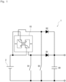
- the circuit 1 is a non-isolated boost converter to which a DC power supply 2 is connected.
- the joining inductor 10 includes a core 11, a first winding 13, and a second winding 14.
- the core 11, the first winding 13, and the second winding 14 are insulated from each other.
- the joining inductor 10 includes a bobbin 12 (shown in Fig. 3 ) that covers a first leg 23 of the core 11 to be described later.
- the core 11 includes a core body 20.
- the core body 20 includes a first core window 21, a second core window 22, and three legs (hereinafter referred to as the first leg 23, the second leg 24, and the third leg 25).
- the first core window 21 and the second core window 22 are spaced apart in a first direction (for example, in the X direction). Each of the first core window 21 and the second core window 22 penetrates the core body 20 in a second direction (for example, in the Y direction) intersecting the first direction X.
- the first leg 23 is located between the first core window 21 and the second core window 22.
- the second leg 24 is located on one side of the first leg 23 in the first direction X, and the first core window 21 is located between the second leg 24 and the first leg 23.
- the third leg 25 is located on the other side of the first leg 23 in the first direction X, and the second core window 22 is located between the third leg 25 and the first leg 23.
- Each of the first leg 23, the second leg 24, and the third leg 25 extends along a third direction (for example, in the Z direction,) intersecting the first direction X and the second direction Y, and includes one gap 231, 241, or 251 in a middle thereof.
- the gaps 231, 241, and 251 of the respective legs are formed by gaps (In other words, gap spaces).
- the core body 20 has a substantially rectangular parallelepiped shape as a whole, and includes two members 201 and 202.
- Each of the members 201 and 202 is made of ferrite, for example, and has a substantially E-shape when viewed along the second direction Y.
- the members 201 and 202 are located symmetrically with respect to an imaginary line L passing through the center of the core body 20 in the third direction Z with an interval therebetween in the third direction Z.
- the first winding 13 is wound around the first leg 23 and includes winding ends 131, 132 positioned at the first core window 21.
- the first winding 13 is wound around the first leg 23 to start winding from the first core window 21 and finish winding at the first core window 21.
- the second winding 14 is wound around the first leg 23 and includes winding ends 141, 142 positioned at the second core window 22.
- the second winding 14 is wound around the first leg 23 to start winding from the second core window 22 and finish winding at the second core window 22.
- Each of the first winding 13 and the second winding 14 is wound around the first leg 23 by N.5 turns (N is a natural number) (in other words, wound around the first leg 23 by a fractional number of turns).
- N is a natural number
- each of the first winding 13 and the second winding 14 is wound around the first leg 23 by 1.5 turns.
- the joining inductor 10 and the circuit 1 can exhibit the following effects.
- the joining inductor 10 includes a core 11, a first winding 13, and a second winding 14.
- the core 11 includes a core body 20.
- the core body 20 includes a first core window 21, a second core window 22, a first leg 23, a second leg 24, and a third leg 25.
- the first core window 21 and the second core window 22 are positioned at an interval in the first direction X and penetrate the core body 20 in the second direction Y.
- the first leg 23 is positioned between the first core window 21 and the second core window 22.
- the second leg 24 is located on one side of the first leg 23 in the first direction X, and the first core window 21 is located between the second leg 24 and the first leg 23.
- the second leg 24 is located on the other side of the first leg 23 in the first direction X, and the second core window 22 is located between the second leg 24 and the first leg 23.
- the first winding 13 is wound around the first leg 23 and includes winding ends 131, 132 positioned at the first core window 21.
- the second winding 14 is wound around the first leg 23 and includes winding ends 141, 142 positioned at the second core window 22.
- Each of the first leg 23, the second leg 24, and the third leg 25 includes at least one gap 231, 241 or 251 in the third direction Z.
- the joining inductor 10 can downsize in the winding thickness direction (that is, the first direction X) of the first winding 13 and the second winding 14.
- the circuit 1 can realize a circuit that can downsize by the joining inductor 10.
- the joining inductor 10 and the circuit 1 may be configured as follows.
- each of the first leg 23, the second leg 24, and the third leg 25 may include a plurality of gaps 231, 241, and 251 in the third direction Z.
- the fringing effect between the two members 201 and 202 of the core body 20 can be inhibited.
- insulating sheets (in other words, spacer) and magnetic members 232, 242, and 252 are alternately arranged along the third direction Z, and the spacers constitute the gaps 231, 241, and 251 of the respective legs.
- the gaps 231, 241, and 251 of each leg may all be configured with gaps of the same size or may be configured to include gaps of different sizes.
- the first winding 13 and the second winding 14 may be configured of any winding including a single wire, a Litz wire, an edgewise wire and a PCB winding. For example, by configuring the first winding 13 and the second winding 14 with edgewise windings or PCB windings, losses at high frequencies can be reduced.
- the standards of the first winding 13 and the second winding 14 are set according to, for example, the design, application, and the like of the joining inductor 10.
- the first winding 13 and the second winding 14 may be wound around the first leg 23 in a state of being twisted with each other. With this configuration, the degree of magnetic coupling can be increased.
- the core 11 may be configured such that width W1 of the gap 231 of the first leg 23 is larger than widths W2, W3 of the gaps 241, 251 of the second leg 24 and the third leg 25.
- width W2 of the gap 241 of the second leg 24 is equal to the width W3 of the gap 251 of the third leg 25.
- FIG. 7 A relationship between a coupling coefficient and a ratio of the width W2 and the width W3 to the width W1 is illustrated in Fig. 7 .
- a horizontal axis represents a ratio of the width W2 to the width W1 and a ratio of the width W3 to the width W1
- a vertical axis represents the coupling coefficient.
- the relationship between the coupling coefficient and the ratio of the width W2 and the width W3 to the width W1 in the case of using the joining inductor 10 in which the first winding 13 and the second winding 14 are wound 6.5 turns around the first leg 23 (hereinafter referred to as a first joining inductor 10) is indicated by a solid line.
- the relationship between the coupling coefficient and the ratio of the width W2 and the width W3 to the width W1 in a case of using the joining inductor 10 in which the first winding 13 and the second winding 14 are wound 3.5 turns around the first leg 23 (hereinafter referred to as a second joining inductor 10) is indicated by a dotted line.
- the coupling coefficient is 0.9 or more in any joining inductor 10. It was found that when the ratio of the width W2 and the width W3 to the width W1 is greater than 1, the coupling coefficient is smaller than when the ratio of the width W2 and the width W3 to the width W1 is smaller than 1. It was found that the second joining inductor 10 is more susceptible to variations in the ratio of the width W2 and the width W3 to the width W1 than the first joining inductor 10.
- the core 11 by configuring the core 11 such that the width W1 of the gap 231 of the first leg 23 is larger than the widths W2 and W3 of the gaps 241 and 251 of the second leg 24 and the third leg 25, a degree of magnetic coupling can be increased.
- the coupling coefficient can be adjusted by adjusting the ratio of the width W2 and the width W3 to the width W1.
- the joining inductor 10 is not limited to a two-phase inductor, and may be used as an inductor of three or more phases.
- the third winding is wound around the first leg 23 by N.5 turns. Winding ends of the third winding may be located in the first core window 21 or the second core window 22.
- the two members 201 and 202 constituting the core body 20 are not limited to the case where both of them are substantially E-shaped when viewed along the second direction Y.
- one of the two members 201 and 202 may have a substantially I shape when viewed along the second direction Y.
- the bobbin 12 may be omitted.
- the core 11 and each winding can be insulated from each other.
- the gaps 231, 241, and 251 of each leg can be formed of, for example, a spacer.
- the circuit 1 is not limited to a non-isolated boost converter.
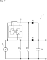
- the circuit 1 may be, for example, a non-isolated step-down converter to which the DC power supply 2 is connected as illustrated in Fig. 8 , or may be a power factor correction (PFC) converter to which the AC power supply 3 is connected as illustrated in Fig. 9 .
- PFC power factor correction
- the joining inductor 10 includes:
- each of the first leg 23, the second leg 24, and the third leg 25 has a plurality of gaps 231, 241, and 251 in the third direction.
- the first winding 13 and the second winding 14 are wound around the first leg 23 in a state of being twisted with each other.
- the circuit 1 according to a sixth aspect of the present disclosure includes the joining inductor 10 according to the above aspect.
- the joining inductor of the present disclosure can be applied to, for example, a non-isolated boost converter.
- the circuit of the present disclosure can be applied to, for example, a general-purpose power supply and an electric vehicle.
Landscapes
- Engineering & Computer Science (AREA)
- Power Engineering (AREA)
- Chemical & Material Sciences (AREA)
- Composite Materials (AREA)
- Coils Of Transformers For General Uses (AREA)
- Coils Or Transformers For Communication (AREA)
Abstract
Description
- The present disclosure relates to a joining inductor and a circuit comprising the joining inductor.
-
Patent Document 1 discloses a reactor for a multiphase converter. The reactor comprises a core including a central leg and end legs located on both sides of the central leg. - Patent Document 1:
JP-A-2012-65453 - In the reactor of
Patent Document 1, since a converter coil is wound around the end leg of the core, it may be difficult to downsize in a winding thickness direction of the converter coil. - An object of the present disclosure is to provide a joining inductor that can downsize and a circuit including the joining inductor.
- A joining inductor according to an aspect of the present disclosure includes:
- a core including a core body, the core body including a first core window, a second core window, a first leg, a second leg, and a third leg, the first core window and the second core window being positioned at an interval in a first direction and each penetrating the core body in a second direction intersecting the first direction, the first leg being positioned between the first core window and the second core window, the second leg being positioned on one side of the first leg in the first direction, the first core window being positioned between the first leg and the second leg, the third leg being positioned on another side of the first leg in the first direction, the second core window being positioned between the first leg and the third leg;
- a first winding wound around the first leg and including winding ends positioned at the first core window; and
- a second winding wound around the first leg and including winding ends positioned at the second core window, wherein
- each of the first leg, the second leg, and the third leg includes at least one gap in a third direction intersecting the first direction and the second direction.
- A circuit according to one aspect of the present disclosure includes the joining inductor according to the above aspect.
- According to the joining inductor of the above aspect, it is possible to realize a joining inductor that can downsize.
- According to the circuit of the above aspect, it is possible to realize a circuit that can downsize by the joining inductor.
-
-
Fig. 1 is a configuration diagram illustrating a circuit including a joining inductor according to an embodiment of the present disclosure. -
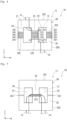
Fig. 2 is a perspective view of the joining inductor ofFig. 1 . -
Fig. 3 is a schematic front view of the joining inductor ofFig. 1 -
Fig. 4 is a schematic front view illustrating a first modification of the joining inductor ofFig. 1 . -
Fig. 5 is a schematic front view illustrating a second modification of the joining inductor ofFig. 1 . -
Fig. 6 is a schematic front view illustrating a third modification of the joining inductor ofFig. 1 . -
Fig. 7 is a graph showing a relationship between a coupling coefficient and a ratio of the gap of the second leg and the gap of the second leg to the gap of the first leg. -
Fig. 8 is a configuration diagram illustrating a first modification of the circuit ofFig. 1 . -
Fig. 9 is a configuration diagram illustrating a second modification of the circuit ofFig. 1 . - Hereinafter, an example of the present disclosure will be described with reference to the accompanying drawings. The following description is merely exemplary in nature and is not intended to limit the present disclosure, its application, or its use. The accompanying drawings are schematic, and ratios of dimensions and the like do not necessarily match actual ones.
- As illustrated in
Fig. 1 , a joininginductor 10 according to an embodiment of the present disclosure constitutes a part of acircuit 1. In the present embodiment, thecircuit 1 is a non-isolated boost converter to which aDC power supply 2 is connected. - As illustrated in
Figs. 2 and 3 , the joininginductor 10 includes acore 11, a first winding 13, and asecond winding 14. Thecore 11, the first winding 13, and the second winding 14 are insulated from each other. In the present embodiment, the joininginductor 10 includes a bobbin 12 (shown inFig. 3 ) that covers afirst leg 23 of thecore 11 to be described later. - As illustrated in
Fig. 3 , thecore 11 includes acore body 20. Thecore body 20 includes afirst core window 21, asecond core window 22, and three legs (hereinafter referred to as thefirst leg 23, thesecond leg 24, and the third leg 25). - The
first core window 21 and thesecond core window 22 are spaced apart in a first direction (for example, in the X direction). Each of thefirst core window 21 and thesecond core window 22 penetrates thecore body 20 in a second direction (for example, in the Y direction) intersecting the first direction X. - The
first leg 23 is located between thefirst core window 21 and thesecond core window 22. Thesecond leg 24 is located on one side of thefirst leg 23 in the first direction X, and thefirst core window 21 is located between thesecond leg 24 and thefirst leg 23. Thethird leg 25 is located on the other side of thefirst leg 23 in the first direction X, and thesecond core window 22 is located between thethird leg 25 and thefirst leg 23. Each of thefirst leg 23, thesecond leg 24, and thethird leg 25 extends along a third direction (for example, in the Z direction,) intersecting the first direction X and the second direction Y, and includes onegap gaps - In the present embodiment, the
core body 20 has a substantially rectangular parallelepiped shape as a whole, and includes twomembers members members core body 20 in the third direction Z with an interval therebetween in the third direction Z. - The
first winding 13 is wound around thefirst leg 23 and includes windingends first core window 21. In other words, thefirst winding 13 is wound around thefirst leg 23 to start winding from thefirst core window 21 and finish winding at thefirst core window 21. - The
second winding 14 is wound around thefirst leg 23 and includes windingends second core window 22. In other words, the second winding 14 is wound around thefirst leg 23 to start winding from thesecond core window 22 and finish winding at thesecond core window 22. - Each of the first winding 13 and the second winding 14 is wound around the
first leg 23 by N.5 turns (N is a natural number) (in other words, wound around thefirst leg 23 by a fractional number of turns). In the present embodiment, each of the first winding 13 and the second winding 14 is wound around thefirst leg 23 by 1.5 turns. - The joining
inductor 10 and thecircuit 1 can exhibit the following effects. - The joining
inductor 10 includes acore 11, a first winding 13, and a second winding 14. Thecore 11 includes acore body 20. Thecore body 20 includes afirst core window 21, asecond core window 22, afirst leg 23, asecond leg 24, and athird leg 25. Thefirst core window 21 and thesecond core window 22 are positioned at an interval in the first direction X and penetrate thecore body 20 in the second direction Y. Thefirst leg 23 is positioned between thefirst core window 21 and thesecond core window 22. Thesecond leg 24 is located on one side of thefirst leg 23 in the first direction X, and thefirst core window 21 is located between thesecond leg 24 and thefirst leg 23. Thesecond leg 24 is located on the other side of thefirst leg 23 in the first direction X, and thesecond core window 22 is located between thesecond leg 24 and thefirst leg 23. The first winding 13 is wound around thefirst leg 23 and includes winding ends 131, 132 positioned at thefirst core window 21. The second winding 14 is wound around thefirst leg 23 and includes winding ends 141, 142 positioned at thesecond core window 22. Each of thefirst leg 23, thesecond leg 24, and thethird leg 25 includes at least onegap second leg 24 and thethird leg 25 located outside thefirst leg 23 in the first direction X, the joininginductor 10 can downsize in the winding thickness direction (that is, the first direction X) of the first winding 13 and the second winding 14. - In general, in a case where the winding is wound around the
second leg 24 and thethird leg 25, a special bobbin that covers thesecond leg 24 and thethird leg 25 is required, and the manufacturing cost increases. In the joininginductor 10, since the winding is wound only around thefirst leg 23, a special bobbin is not required, and an increase in manufacturing cost can be suppressed. - The
circuit 1 can realize a circuit that can downsize by the joininginductor 10. - The joining
inductor 10 and thecircuit 1 may be configured as follows. - As illustrated in
Fig. 4 , each of thefirst leg 23, thesecond leg 24, and thethird leg 25 may include a plurality ofgaps members core body 20 can be inhibited. In the joininginductor 10 ofFig. 4 , as an example, insulating sheets (in other words, spacer) andmagnetic members gaps gaps - The first winding 13 and the second winding 14 may be configured of any winding including a single wire, a Litz wire, an edgewise wire and a PCB winding. For example, by configuring the first winding 13 and the second winding 14 with edgewise windings or PCB windings, losses at high frequencies can be reduced. The standards of the first winding 13 and the second winding 14 are set according to, for example, the design, application, and the like of the joining
inductor 10. - As illustrated in
Fig. 5 , the first winding 13 and the second winding 14 may be wound around thefirst leg 23 in a state of being twisted with each other. With this configuration, the degree of magnetic coupling can be increased. - As illustrated in
Fig. 6 , thecore 11 may be configured such that width W1 of thegap 231 of thefirst leg 23 is larger than widths W2, W3 of thegaps second leg 24 and thethird leg 25. In the joininginductor 10 ofFig. 6 , the width W2 of thegap 241 of thesecond leg 24 is equal to the width W3 of thegap 251 of thethird leg 25. - A relationship between a coupling coefficient and a ratio of the width W2 and the width W3 to the width W1 is illustrated in
Fig. 7 . InFig. 7 , a horizontal axis represents a ratio of the width W2 to the width W1 and a ratio of the width W3 to the width W1, and a vertical axis represents the coupling coefficient. The relationship between the coupling coefficient and the ratio of the width W2 and the width W3 to the width W1 in the case of using the joininginductor 10 in which the first winding 13 and the second winding 14 are wound 6.5 turns around the first leg 23 (hereinafter referred to as a first joining inductor 10) is indicated by a solid line. The relationship between the coupling coefficient and the ratio of the width W2 and the width W3 to the width W1 in a case of using the joininginductor 10 in which the first winding 13 and the second winding 14 are wound 3.5 turns around the first leg 23 (hereinafter referred to as a second joining inductor 10) is indicated by a dotted line. - It was found that, as illustrated in
Fig. 7 , when the ratio of the width W2 and the width W3 to the width W1 is smaller than 1, the coupling coefficient is 0.9 or more in any joininginductor 10. It was found that when the ratio of the width W2 and the width W3 to the width W1 is greater than 1, the coupling coefficient is smaller than when the ratio of the width W2 and the width W3 to the width W1 is smaller than 1. It was found that the second joininginductor 10 is more susceptible to variations in the ratio of the width W2 and the width W3 to the width W1 than the first joininginductor 10. - That is, by configuring the core 11 such that the width W1 of the
gap 231 of thefirst leg 23 is larger than the widths W2 and W3 of thegaps second leg 24 and thethird leg 25, a degree of magnetic coupling can be increased. The coupling coefficient can be adjusted by adjusting the ratio of the width W2 and the width W3 to the width W1. - The joining
inductor 10 is not limited to a two-phase inductor, and may be used as an inductor of three or more phases. For example, when the joininginductor 10 is used as a three-phase inductor, in addition to the first winding 13 and the second winding 14, the third winding is wound around thefirst leg 23 by N.5 turns. Winding ends of the third winding may be located in thefirst core window 21 or thesecond core window 22. - The two
members core body 20 are not limited to the case where both of them are substantially E-shaped when viewed along the second direction Y. For example, one of the twomembers - The
bobbin 12 may be omitted. In this case, for example, by covering each winding with an insulating film, thecore 11 and each winding can be insulated from each other. Thegaps - The
circuit 1 is not limited to a non-isolated boost converter. Thecircuit 1 may be, for example, a non-isolated step-down converter to which theDC power supply 2 is connected as illustrated inFig. 8 , or may be a power factor correction (PFC) converter to which theAC power supply 3 is connected as illustrated inFig. 9 . - Various embodiments of the present disclosure have been described above in detail with reference to the drawings. Finally, various aspects of the present disclosure will be described. In the following description, as an example, reference numerals are also added.
- The joining
inductor 10 according to a first aspect of the present disclosure includes: - a core 11 including a
core body 20, thecore body 20 including afirst core window 21, asecond core window 22, afirst leg 23, asecond leg 24, and athird leg 25, thefirst core window 21 and thesecond core window 22 being positioned at an interval in a first direction and each penetrating thecore body 20 in a second direction intersecting the first direction, thefirst leg 23 being positioned between thefirst core window 21 and thesecond core window 22, thesecond leg 24 being positioned on one side of thefirst leg 23 in the first direction, thefirst core window 21 being positioned between thefirst leg 23 and thesecond leg 24, thethird leg 25 being positioned on another side of thefirst leg 23 in the first direction, thesecond core window 22 being positioned between thefirst leg 23 and thethird leg 25; - a first winding 13 wound around the
first leg 23 and including winding ends 131, 132 positioned at thefirst core window 21; and - a second winding 14 wound around the
first leg 23 and including winding ends 141, 142 positioned at thesecond core window 22, wherein - each of the
first leg 23, thesecond leg 24, and thethird leg 25 includes at least onegap - In the joining
inductor 10 according to a second aspect of the present disclosure,
each of thefirst leg 23, thesecond leg 24, and thethird leg 25 has a plurality ofgaps - In the joining
inductor 10 according to a third aspect of the present disclosure,
the first winding 13 and the second winding 14 are edgewise windings or PCB windings. - In the joining
inductor 10 according to a fourth aspect of the present disclosure,
the first winding 13 and the second winding 14 are wound around thefirst leg 23 in a state of being twisted with each other. - In the joining
inductor 10 according to a fifth aspect of the present disclosure, thegap 231 of thefirst leg 23 is larger than thegaps second leg 24 and thethird leg 25. - The
circuit 1 according to a sixth aspect of the present disclosure includes
the joininginductor 10 according to the above aspect. - By appropriately combining arbitrary embodiments or modifications among the various embodiments or modifications, it is possible to achieve the respective effects. In addition, combinations of embodiments, combinations of examples, or combinations of embodiments and examples are possible, and combinations of features in different embodiments or examples are also possible.
- Although the present disclosure has been fully described in connection with preferred embodiment with reference to the accompanying drawings, various changes and modifications are obvious to those skilled in the art. Such changes and modifications are to be understood as being encompassed in the scope of the present disclosure as set forth in the appended claims.
- The joining inductor of the present disclosure can be applied to, for example, a non-isolated boost converter.
- The circuit of the present disclosure can be applied to, for example, a general-purpose power supply and an electric vehicle.
-
- 1 Circuit
- 2 DC power supply
- 3 AC power supply
- 10 Joining inductor
- 11 Core
- 12 Bobbin
- 13 First winding
- 131, 132 Winding end
- 14 Second winding
- 141, 142 Winding end
- 20 Core body
- 201,202 Member
- 21 First core window
- 22 Second core window
- 23 First leg
- 231 Gap
- 232 Member
- 24 Second leg
- 241 Gap
- 242 Member
- 25 Third leg
- 251 Gap
- 252 Member
Claims (6)
- A joining inductor, comprising:a core including a core body, the core body including a first core window, a second core window, a first leg, a second leg, and a third leg, the first core window and the second core window being positioned at an interval in a first direction and each penetrating the core body in a second direction intersecting the first direction, the first leg being positioned between the first core window and the second core window, the second leg being positioned on one side of the first leg in the first direction, the first core window being positioned between the first leg and the second leg, the third leg being positioned on another side of the first leg in the first direction, the second core window being positioned between the first leg and the third leg;a first winding wound around the first leg and including winding ends positioned at the first core window; anda second winding wound around the first leg and including winding ends positioned at the second core window, whereineach of the first leg, the second leg, and the third leg includes at least one gap in a third direction intersecting the first direction and the second direction.
- The joining inductor according to claim 1, wherein
each of the first leg, the second leg, and the third leg has a plurality of gaps in the third direction. - The joining inductor according to claim 1 or 2, wherein
the first winding and the second winding are edgewise windings or PCB windings. - The joining inductor according to any one of claims 1 to 3, wherein
the first winding and the second winding are wound around the first leg in a state of being twisted with each other. - The joining inductor according to any one of claims 1 to 4, wherein,
the gap of the first leg is larger than the gaps of the second leg and the third leg. - A circuit, comprising:
the joining inductor according to any one of claims 1 to 5.
Applications Claiming Priority (2)
| Application Number | Priority Date | Filing Date | Title |
|---|---|---|---|
| JP2022033796A JP2023129039A (en) | 2022-03-04 | 2022-03-04 | Coupled inductors and circuits |
| PCT/JP2023/003605 WO2023166914A1 (en) | 2022-03-04 | 2023-02-03 | Joining inductor and circuit |
Publications (2)
| Publication Number | Publication Date |
|---|---|
| EP4489042A1 true EP4489042A1 (en) | 2025-01-08 |
| EP4489042A4 EP4489042A4 (en) | 2026-03-18 |
Family
ID=87883340
Family Applications (1)
| Application Number | Title | Priority Date | Filing Date |
|---|---|---|---|
| EP23763176.7A Pending EP4489042A4 (en) | 2022-03-04 | 2023-02-03 | CONNECTING INDUCTOR AND CIRCUIT |
Country Status (5)
| Country | Link |
|---|---|
| US (1) | US20250191837A1 (en) |
| EP (1) | EP4489042A4 (en) |
| JP (1) | JP2023129039A (en) |
| CN (1) | CN118843913A (en) |
| WO (1) | WO2023166914A1 (en) |
Family Cites Families (14)
| Publication number | Priority date | Publication date | Assignee | Title |
|---|---|---|---|---|
| JPH0457304A (en) * | 1990-06-27 | 1992-02-25 | Matsushita Electric Ind Co Ltd | converter transformer |
| JP2000195723A (en) * | 1998-12-28 | 2000-07-14 | Sumida Electric Co Ltd | Inductance element |
| JP4873534B2 (en) * | 2005-12-09 | 2012-02-08 | Necトーキン株式会社 | Inductor |
| WO2008087885A1 (en) * | 2007-01-15 | 2008-07-24 | Hitachi Metals, Ltd. | Reactor core and reactor |
| JP5081063B2 (en) * | 2008-05-22 | 2012-11-21 | 本田技研工業株式会社 | Composite transformer and power conversion circuit |
| JP2010263028A (en) * | 2009-05-01 | 2010-11-18 | Panasonic Corp | Resonant coil and resonant transformer |
| JP5502672B2 (en) | 2010-09-16 | 2014-05-28 | 株式会社豊田中央研究所 | Multi-phase converter reactor |
| US8576037B1 (en) * | 2011-05-04 | 2013-11-05 | Scientific Components Corporation | Dual output autotransformer |
| JP2015141997A (en) * | 2014-01-28 | 2015-08-03 | Jfeスチール株式会社 | Reactor core, and reactor using the same |
| JP6424497B2 (en) * | 2014-07-03 | 2018-11-21 | 富士通株式会社 | Planar transformer, power supply unit, and method of manufacturing planar transformer |
| CN108809079B (en) * | 2017-05-05 | 2019-11-05 | 台达电子企业管理(上海)有限公司 | Power inverter, inductance element and inductance cut off control method |
| KR102767117B1 (en) * | 2020-01-31 | 2025-02-14 | 엘지이노텍 주식회사 | Transformer and flat panel display device including the same |
| JP7373119B2 (en) * | 2020-02-19 | 2023-11-02 | スミダコーポレーション株式会社 | magnetically coupled inductor |
| JPWO2022044803A1 (en) * | 2020-08-28 | 2022-03-03 |
-
2022
- 2022-03-04 JP JP2022033796A patent/JP2023129039A/en active Pending
-
2023
- 2023-02-03 EP EP23763176.7A patent/EP4489042A4/en active Pending
- 2023-02-03 WO PCT/JP2023/003605 patent/WO2023166914A1/en not_active Ceased
- 2023-02-03 CN CN202380025343.0A patent/CN118843913A/en active Pending
- 2023-02-03 US US18/843,449 patent/US20250191837A1/en active Pending
Also Published As
| Publication number | Publication date |
|---|---|
| WO2023166914A1 (en) | 2023-09-07 |
| JP2023129039A (en) | 2023-09-14 |
| EP4489042A4 (en) | 2026-03-18 |
| US20250191837A1 (en) | 2025-06-12 |
| CN118843913A (en) | 2024-10-25 |
Similar Documents
| Publication | Publication Date | Title |
|---|---|---|
| US7280026B2 (en) | Extended E matrix integrated magnetics (MIM) core | |
| JP4800451B1 (en) | High frequency transformer | |
| EP2323143B1 (en) | Three-phase high frequency transformer | |
| EP2498266A2 (en) | Reactor and power converter using the same | |
| US9899144B2 (en) | Resonant high current density transformer | |
| CN210378713U (en) | Resonant transformer | |
| US20230396180A1 (en) | Integrated transformers for high current converters | |
| US9287035B2 (en) | Flyback converter using coaxial cable transformer | |
| KR20140041867A (en) | Reactor and electrical device | |
| JPH08316054A (en) | Thin transformer | |
| JPH11144971A (en) | Coil component and power supply device using the same | |
| US6861938B2 (en) | High-frequency power inductance element | |
| JP4845199B2 (en) | Trance | |
| CN114068153A (en) | Low Profile High Current Coupled Winding Electromagnetic Components | |
| JP2002353045A (en) | Power transformer and power conversion device using the same | |
| US20250191837A1 (en) | Joining inductor and circuit | |
| JP2016146441A (en) | Transformer and manufacturing method thereof | |
| US20100123537A1 (en) | Planar coil component | |
| US20150279549A1 (en) | Systems and methods for promoting low loss in parallel conductors at high frequencies | |
| US6784781B1 (en) | Reactor and ballast system | |
| JP2008205212A (en) | Transformer | |
| CN115910524A (en) | Integrated magnetic components, PFC circuits and electronic equipment | |
| EP4303897A1 (en) | Magnetic core | |
| US7750526B2 (en) | Circulatory current choke | |
| US20240203637A1 (en) | Winding arrangement for transformer |
Legal Events
| Date | Code | Title | Description |
|---|---|---|---|
| STAA | Information on the status of an ep patent application or granted ep patent |
Free format text: STATUS: THE INTERNATIONAL PUBLICATION HAS BEEN MADE |
|
| PUAI | Public reference made under article 153(3) epc to a published international application that has entered the european phase |
Free format text: ORIGINAL CODE: 0009012 |
|
| STAA | Information on the status of an ep patent application or granted ep patent |
Free format text: STATUS: REQUEST FOR EXAMINATION WAS MADE |
|
| 17P | Request for examination filed |
Effective date: 20240830 |
|
| AK | Designated contracting states |
Kind code of ref document: A1 Designated state(s): AL AT BE BG CH CY CZ DE DK EE ES FI FR GB GR HR HU IE IS IT LI LT LU LV MC ME MK MT NL NO PL PT RO RS SE SI SK SM TR |
|
| DAV | Request for validation of the european patent (deleted) | ||
| DAX | Request for extension of the european patent (deleted) | ||
| A4 | Supplementary search report drawn up and despatched |
Effective date: 20260213 |
|
| RIC1 | Information provided on ipc code assigned before grant |
Ipc: H01F 37/00 20060101AFI20260209BHEP Ipc: H01F 3/14 20060101ALI20260209BHEP Ipc: H02M 1/42 20070101ALI20260209BHEP Ipc: H02M 3/158 20060101ALI20260209BHEP |