EP4488875A1 - Rfid sensor device and method of manufacturing the same - Google Patents
Rfid sensor device and method of manufacturing the same Download PDFInfo
- Publication number
- EP4488875A1 EP4488875A1 EP23184078.6A EP23184078A EP4488875A1 EP 4488875 A1 EP4488875 A1 EP 4488875A1 EP 23184078 A EP23184078 A EP 23184078A EP 4488875 A1 EP4488875 A1 EP 4488875A1
- Authority
- EP
- European Patent Office
- Prior art keywords
- rfid
- substrate
- spacer
- sensor device
- rfid chip
- Prior art date
- Legal status (The legal status is an assumption and is not a legal conclusion. Google has not performed a legal analysis and makes no representation as to the accuracy of the status listed.)
- Pending
Links
Images


Classifications
-
- G—PHYSICS
- G06—COMPUTING OR CALCULATING; COUNTING
- G06K—GRAPHICAL DATA READING; PRESENTATION OF DATA; RECORD CARRIERS; HANDLING RECORD CARRIERS
- G06K19/00—Record carriers for use with machines and with at least a part designed to carry digital markings
- G06K19/06—Record carriers for use with machines and with at least a part designed to carry digital markings characterised by the kind of the digital marking, e.g. shape, nature, code
- G06K19/067—Record carriers with conductive marks, printed circuits or semiconductor circuit elements, e.g. credit or identity cards also with resonating or responding marks without active components
- G06K19/07—Record carriers with conductive marks, printed circuits or semiconductor circuit elements, e.g. credit or identity cards also with resonating or responding marks without active components with integrated circuit chips
- G06K19/0716—Record carriers with conductive marks, printed circuits or semiconductor circuit elements, e.g. credit or identity cards also with resonating or responding marks without active components with integrated circuit chips at least one of the integrated circuit chips comprising a sensor or an interface to a sensor
- G06K19/0717—Record carriers with conductive marks, printed circuits or semiconductor circuit elements, e.g. credit or identity cards also with resonating or responding marks without active components with integrated circuit chips at least one of the integrated circuit chips comprising a sensor or an interface to a sensor the sensor being capable of sensing environmental conditions such as temperature history or pressure
-
- G—PHYSICS
- G06—COMPUTING OR CALCULATING; COUNTING
- G06K—GRAPHICAL DATA READING; PRESENTATION OF DATA; RECORD CARRIERS; HANDLING RECORD CARRIERS
- G06K19/00—Record carriers for use with machines and with at least a part designed to carry digital markings
- G06K19/04—Record carriers for use with machines and with at least a part designed to carry digital markings characterised by the shape
- G06K19/041—Constructional details
Definitions
- the present disclosure generally relates to radio frequency identification (RFID) devices, in particular, to an RFID sensor device and a method of manufacturing the same.
- RFID radio frequency identification
- RFID devices such as, for example, RFID cards, RFID tags, etc.
- RFID devices include an RFID antenna and an integrated circuit provided on an RFID chip and connected to the RFID antenna.
- the RFID antenna Upon presence of an electromagnetic field emitted by a reader device, the RFID antenna supplies energy from the electromagnetic field to the integrated circuit, which integrated circuit may communicate with the reader device using radio frequency (RF) communication protocols.
- RF radio frequency
- the RFID chip not only performs the usual RFID communications via the RFID antenna, but also transmits detection results from a sensing element integrated into the RFID chip.
- a sensor signal from the sensing element is converted to a modulated RF signal and transmitted via the RFID antenna.
- the present disclosure is directed, at least in part, to improving or overcoming one or more aspects of prior systems.
- an RIFD sensor device comprises a substrate having a first surface and an opposite second surface, an RIFD antenna provided on the substrate, and an RFID chip mounted on the first surface of the substrate.
- the RFID chip is configured to perform RFID communications via the RFID antenna and includes a sensing circuitry for sensing at least one physical quantity.
- a spacer is provided on the first surface of the substrate. The spacer includes an opening extending through the spacer. The RFID chip is mounted inside the opening.
- a method of manufacturing an RFID sensor device comprises the steps of providing a substrate having a first surface and an opposite second surface, an RFID antenna provided on the substrate, mounting an RFID chip on the first surface of the substrate, the RFID chip being configured to perform RFID communications via the RFID antenna, and including sensing circuitry for sensing at least one physical quantity, and providing a spacer on the first surface of the substrate.
- the spacer includes an opening extending through the spacer, and the RFID chip is mounted inside the opening.
- the present disclosure is based at least in part on the realization that, for an RFID chip including a sensing capability, the required antenna connection and transponder packaging are strongly influencing the capability or sensitivity of detecting the desired physical parameter.
- the surrounding packaging material will isolate the chip from the sensing surface, resulting in inaccurate measurement values due to a thermal gradient and/or thermal inertia.
- any packaging material placed between the surface to be monitored and the RFID chip acts as a stress relief and strongly reduces the measurement sensitivity.
- the passive RFID transponder it has been realized that the above problems can be overcome by using a specific packaging and mounting method of the passive RFID transponder.
- a polymer spacer for example, a polymer foil, with a thickness that is slightly higher than the chip thickness is attached to the antenna substrate.
- the polymer layer or foil has an opening in the chip area, and acts as a spacer for further packaging of the full transponder.
- the polymer spacer keeps the opening free of any packaging material that could influence the sensing capability of the RFID chip.
- the passive sensing RFID chip remains unprotected and is suitable for attaching to the surface to be monitored.
- the RFID chip can be mounted in close proximity to said surface to be monitored.
- the present disclosure is also based at least in part on the realization that, depending on the final packaging process, small vias (i.e., passages or through-holes) can be provided in the antenna substrate adjacent to the RFID chip. Said vias can be used for the injection of an appropriate filler material to fill the gaps between the RFID chip and the inner peripheral surface of the opening in the spacer, as well as any remaining gap between the RFID chip and the surface to be monitored. In this manner, the RFID chip can be further protected, while at the same time maintaining the close proximity to the surface to be monitored.
- small vias i.e., passages or through-holes
- the thickness of the polymer spacer can be selected in accordance with the further packaging, for example, to minimize the gap between the chip and a surface to be monitored, and/or to set the distance between the chip and the surface to be monitored to a desired value. In this manner, the sensing capability of the RFID sensor device can be maximized for the best results in terms of accuracy and dynamic response.
- Fig. 1 shows a schematic perspective view of an RFID sensor device 10 in accordance with the present disclosure.
- RFID sensor device 10 is attached to a surface S of an object 80 to sense at least one physical quantity of object 80, as will be described in more detail in the following.
- the at least one physical quantity to be monitored can be any desired physical quantity such as temperature, strain, ambient light, relative humidity, and the like.
- object 80 is not limited to any particular object, and can be any desired object, the properties of which are to be monitored.
- One exemplary application is the measurement of the temperature of connection bars in electrical power generators.
- RFID sensor device 10 comprises a housing 22, with a through-hole 24 formed in housing 22.
- the purpose of through-hole 24 will be explained in the following.
- RFID sensor device 10 may have any desired shape, in particular, size and thickness.
- RFID sensor device 10 may have a length of between 50 and 150 mm, a width of between 10 and 50 mm, and a height of between 2 and 20 mm.
- Fig. 2 shows an explosive view of RFID sensor device 10.
- RFID sensor device 10 comprises a substrate 12 having a first surface S1 and an opposite second surface S2.
- An RFID antenna 16 is provided on substrate 12.
- RFID antenna 16 may have any desired and known configuration, and may be formed on substrate 12 in a known manner to facilitate RFID communications.
- An RFID chip 14 is mounted on first surface S1 of substrate 12.
- RFID chip 14 is configured to perform RFID communications via RFID antenna 16 in a known manner.
- RFID chip 14 can be electrically connected to RFID antenna 16 via physical connections, for example, using soldering or the like, or may be inductively coupled to RFID antenna 16.
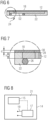
- Fig. 8 shows an exemplary configuration of RFID chip 14, including communications and control circuitry 17, which is connected to RFID antenna 16 (not shown) via terminals 19. Further, as shown in Fig. 8 , RFID chip 14 includes sensing circuitry 15 for sensing at least one physical quantity.
- sensing circuitry 15 may be embodied as a known microelectromechanical systems (MEMS) device, or any other appropriate circuitry that is adapted to sense a physical quantity such as temperature or strain at or adjacent to sensing circuitry 15.
- MEMS microelectromechanical systems
- RFID chips having such a sensing capability include EM
- EM aura-sense
- S900A
- AS321X
- Magnus ® -S AN002
- RFID sensor device 10 further comprises a spacer 18 provided on first surface S1 of substrate 12.
- Spacer 18 includes an opening 20, i.e., a through-hole extending through spacer 18. Opening 20 is formed in spacer 18 in such a manner that, in the state in which spacer 18 is provided on first surface S1, and RFID chip 14 is mounted on first surface S1, RFID chip 14 is mounted (disposed) inside opening 20 (as shown in Fig. 3 ).
- RFID sensor device 10 further comprises an adhesive layer 34, for example, an adhesive tape, and spacer 18 is attached to substrate 12 via adhesive layer 34.
- adhesive layer 34 is only one example for attaching spacer 18 to substrate 12.
- spacer 18 can be provided on substrate 12 in a desired positional relationship, for example, by using a housing or the like that aligns and presses spacer 18 against first surface S1 of substrate 12.
- spacer 18 is arranged such that the bottom surface of the same is in contact with first surface S1 of substrate 12, such that a desired positional relationship between an upper surface of RFID chip 14 and an upper surface of spacer 18 can be obtained.
- the thickness of spacer 18 can be selected such that a gap is formed between an upper surface of RFID chip 14 and an upper surface of spacer 18, with said gap having a desired dimension, for example, between around 50 ⁇ m and around 300 ⁇ m.
- spacer 18 is, for example, configured to be attached to surface S of object 80 to sense the at least one physical quantity of object 80, a desired distance between RFID chip 14, in particular, sensing circuitry 15 of the same, and a surface to be measured can be assured.
- housing 22 accommodates substrate 12 from a side of second surface S2 of substrate 12.
- housing 22 may be box-shaped with a bottom 27 and an outer peripheral wall 29 protruding upwards from bottom 27 and defining an opening of housing 22.
- housing 22 includes a through-hole 24 provided at a position corresponding to opening 20 in spacer 18.
- a sealing element 26, for example, an O-ring is provided between housing 22 and substrate 12. Sealing element 26 is disposed inside through-hole 24.
- a cap 40 may optionally be provided, and may be configured to close through-hole 24. This will be described in more detail in the following.
- Figs. 3, 4 and 5 show a plan view, a side view and a bottom view, respectively, of RFID sensor device 10.
- housing 22 is closed by spacer 18.
- substrate 12, adhesive layer 34, and spacer 18 are arranged in/on housing 22 in this order from the side of housing 22.
- a bottom surface of spacer 18 is in contact with an upper surface of peripheral wall 29 of housing 22 to close housing 22, with substrate 12 being firmly arranged and protected inside housing 22 and spacer 18.
- Fig. 6 shows a cross-sectional view along the line A-A in Fig. 3 .
- housing 22 and spacer 18 are only one example, and that any other appropriate packaging including spacer 18 may be used in order to obtain RFID sensor device 10.
- any appropriate materials can be used, for example, for housing 22, substrate 12, and spacer 18.
- substrate 12 may be formed as a printed circuit board using any known material that is generally used to form such circuit boards.
- spacer 18 may be made from resin, for example, a polymer such as PP, PMMA, PTFE, PET, PC, PA or the like. Similar materials can be used as the material of housing 22, but preferably TPV is used for housing 22.
- housing 22 any other appropriate material can be used for housing 22, as long as it does not affect the signal transmission from RFID chip 14 in a negative manner, and provides the required mechanical stability for protecting substrate 12 and RFID chip 14, at least in case such a protection is necessary.
- housing 22 may be omitted. In such a case, RFID sensor device 10 only comprises substrate 12 and spacer 18, which can again be directly attached to surface S to be monitored.
- a thickness d of spacer 18 may be selected appropriately to obtain the desired distance between RFID chip 14 and surface S to be monitored.
- thickness d of spacer 18 may be between around 50 ⁇ m and around 300 ⁇ m.
- a thickness of RFID chip 14 may also be between around 50 ⁇ m and around 300 ⁇ m. It will be appreciated that, generally, thicknesses of spacer 18 and RFID chip 14 are adapted to each other such that RFID chip 14 does not protrude from opening 20, and remains protected inside opening 20.
- substrate 12 includes at least one via 28 (i.e., at least one through-hole) extending through substrate 12, in particular, at a position adjacent to RFID chip 14.
- At least one via 28 is configured to allow passage of a liquid filler 30 from the side of second surface S2 of substrate 12 into opening 20.
- Filler 30 can be any appropriate material, for example, a glue or the like (examples include Kyowa CC33A, HBM Z70), which can cover RFID chip 14 to further protect the same inside opening 20, and to fill any remaining gap between RFID chip 14 and surface S of object 80 to be monitored.
- filler 30 may be applied after attaching RFID sensor device 10 to surface S of object 80.
- cap 40 may be removed from through-hole 24, and filler 30 may be applied.
- Sealing element 26, for example, an O-ring can reliably prevent leakage of filler 30 inside housing 22.
- filler 30 is selectively supplied to opening 20 via one specific via 28.
- any additional vias in the example shown in Fig. 5 , two additional vias
- any additional vias can be used to detect the filling of opening 20.
- supply of filler 30 can be stopped.
- through-hole 24 can again be closed using cap 40.
- filler 30 is optional. In other words, in some embodiments, no filler 30 is present in opening 20, such that RFID chip 14 is exposed to an outside via opening 20. This may be desirable in some applications where, for example, the presence of filler 30 may negatively affect the measurements to be performed.
- substrate 12 preferably has a thickness h of between around 1 mm and around 5 mm. In this manner, any interference between RFID antenna 16 and the circuitry provided on RFID chip 14 can be reduced or prevented. In this manner, both the connection between RFID chip 14 and RFID antenna 16, and the sensing capability of RFID chip 14 can be improved. This is particularly advantageous if, for example, the surface S to be monitored is electrically conductive.
- an RFID sensor device 10 can be obtained that has a high detection accuracy due to the close proximity between RFID chip 14 and surface S to be monitored. In particular, this is achieved by appropriately selecting the thickness d of spacer 18 and arranging RFID chip 14 inside opening 20 formed in spacer 18.
- RFID sensor device 10 An exemplary method of manufacturing RFID sensor device 10 will be described in the following.
- substrate 12 having first surface S1 and opposite second surface S2 is provided, with RFID antenna 16 being provided on substrate 12 in a known manner, for example, by surface metallization on surfaces S1 and S2 and interconnecting the metallized surfaces using conductive vias.
- RFID chip 14 is mounted on first surface S1 of substrate 12 in a known manner, for example, using flip chip technology.
- RFID chip 14 is configured to perform RFID communications via RFID antenna 16.
- RFID chip 14 includes sensing circuitry 15 for sensing at least one physical quantity such as temperature and strain.
- spacer 18 is provided on first surface S1 of substrate 12, for example, by attaching the same to substrate 12 via adhesive layer 34.
- Spacer 12 includes opening 20 extending through spacer 12, and the position of opening 20 is selected such that RFID chip 14 is mounted inside opening 20 after spacer 18 has been provided on substrate 12.
- the method may further comprise a step of forming housing 22 for accommodating substrate 12.
- housing 22 may be formed by overmolding.
- an overmolding process may be performed using an appropriate die to integrally form housing 22 with said assembly.
- a plurality of protrusions 39 may be formed on housing 22 to protrude into appropriate openings in, for example, substrate 12 and adhesive layer 34 to obtain a firm integration.
- housing 22 may be formed such that it is closed by spacer 18, i.e., the bottom surface of spacer 18 is in contact with the opposed surface of peripheral wall 29 of housing 22 (see also Figs. 6 and 7 ).
- sealing element 26 can be integrated with housing 22 during formation of the same, for example, by the above-mentioned overmolding process.
- sealing element 26 may be mounted on a protrusion of the corresponding die that is in contact with substrate 12.
- housing 22 may be formed in a different manner, for example, in a separate molding process.
- housing 22 may be combined with substrate 12 and spacer 18 in a different manner, for example, by arranging substrate 12 inside housing 22, and attaching spacer 18 to housing 22, for example, using adhesive layer 34.
- RFID sensor device 10 may be attached to surface S of object 80 in an appropriate manner, for example, using an adhesive or the like.
- RFID sensor device 10 may also be attached using screws or rivets, for example, by providing (e.g., drilling) appropriate holes in protrusions 39.
- RFID sensor device 10 can be interrogated using appropriate reader devices in a known manner, to obtain the measurement results of RFID chip 14, in particular, using sensing circuitry 15 provided on the same.
Landscapes
- Engineering & Computer Science (AREA)
- Physics & Mathematics (AREA)
- General Physics & Mathematics (AREA)
- Theoretical Computer Science (AREA)
- Computer Hardware Design (AREA)
- Microelectronics & Electronic Packaging (AREA)
- Arrangements For Transmission Of Measured Signals (AREA)
Abstract
Description
- The present disclosure generally relates to radio frequency identification (RFID) devices, in particular, to an RFID sensor device and a method of manufacturing the same.
- Generally, RFID devices such as, for example, RFID cards, RFID tags, etc. include an RFID antenna and an integrated circuit provided on an RFID chip and connected to the RFID antenna. Upon presence of an electromagnetic field emitted by a reader device, the RFID antenna supplies energy from the electromagnetic field to the integrated circuit, which integrated circuit may communicate with the reader device using radio frequency (RF) communication protocols. In this manner, for example, data can be read from a memory associated with the integrated circuit, and can also be written into said memory, if desired.
- Recently, RFID devices have been used as sensor devices for sensing physical quantities such as temperature, strain, and the like. In such applications, the RFID chip not only performs the usual RFID communications via the RFID antenna, but also transmits detection results from a sensing element integrated into the RFID chip. A sensor signal from the sensing element is converted to a modulated RF signal and transmitted via the RFID antenna.
- The present disclosure is directed, at least in part, to improving or overcoming one or more aspects of prior systems.
- According to one aspect of the present disclosure, an RIFD sensor device comprises a substrate having a first surface and an opposite second surface, an RIFD antenna provided on the substrate, and an RFID chip mounted on the first surface of the substrate. The RFID chip is configured to perform RFID communications via the RFID antenna and includes a sensing circuitry for sensing at least one physical quantity. A spacer is provided on the first surface of the substrate. The spacer includes an opening extending through the spacer. The RFID chip is mounted inside the opening.
- According to another aspect of the present disclosure, a method of manufacturing an RFID sensor device comprises the steps of providing a substrate having a first surface and an opposite second surface, an RFID antenna provided on the substrate, mounting an RFID chip on the first surface of the substrate, the RFID chip being configured to perform RFID communications via the RFID antenna, and including sensing circuitry for sensing at least one physical quantity, and providing a spacer on the first surface of the substrate. The spacer includes an opening extending through the spacer, and the RFID chip is mounted inside the opening.
- Other features and aspects of the present disclosure will be apparent from the following description and the accompanying drawings.
-
-
Fig. 1 is a schematic perspective view showing an RFID sensor device in accordance with the present disclosure attached to an object to be monitored, -
Fig. 2 shows an exemplary explosive view of the RFID sensor device in accordance with the present disclosure, -
Fig. 3 shows a plan view of the RFID sensor device in accordance with the present disclosure, -
Fig. 4 shows a side view of the RFID sensor device in accordance with the present disclosure, -
Fig. 5 shows a bottom view of the RFID sensor device in accordance with the present disclosure, -
Fig. 6 shows a schematic cross-sectional view along the line A-A inFig. 3 , -
Fig. 7 shows an enlarged detail of the cross-sectional view ofFig. 6 , and -
Fig. 8 shows a schematic plan view of an exemplary RFID chip in accordance with the present disclosure. - The following is a detailed description of exemplary embodiments of the present disclosure. The exemplary embodiments described herein are intended to teach the principles of the present disclosure, enabling those of ordinary skill in the art to implement and use the present disclosure in many different environments and for many different applications. Therefore, the exemplary embodiments are not intended to be, and should not be considered as, a limiting description of the scope of protection. Rather, the scope of protection shall be defined by the appended claims.
- The present disclosure is based at least in part on the realization that, for an RFID chip including a sensing capability, the required antenna connection and transponder packaging are strongly influencing the capability or sensitivity of detecting the desired physical parameter. In case of a temperature sensor integrated into the RFID chip, the surrounding packaging material will isolate the chip from the sensing surface, resulting in inaccurate measurement values due to a thermal gradient and/or thermal inertia. In case the RFID chip includes strain sensing capabilities, any packaging material placed between the surface to be monitored and the RFID chip acts as a stress relief and strongly reduces the measurement sensitivity.
- According to the present invention, it has been realized that the above problems can be overcome by using a specific packaging and mounting method of the passive RFID transponder. In particular, after the RFID chip has been placed on an antenna substrate, for example, using flip chip technology, and the electrical connection between the substrate and the chip has been established, for example, using conductive glue, soldering, or a thermos-compression bonding process, a polymer spacer, for example, a polymer foil, with a thickness that is slightly higher than the chip thickness is attached to the antenna substrate. The polymer layer or foil has an opening in the chip area, and acts as a spacer for further packaging of the full transponder. In particular, the polymer spacer keeps the opening free of any packaging material that could influence the sensing capability of the RFID chip. With this configuration, the passive sensing RFID chip remains unprotected and is suitable for attaching to the surface to be monitored. In particular, the RFID chip can be mounted in close proximity to said surface to be monitored.
- The present disclosure is also based at least in part on the realization that, depending on the final packaging process, small vias (i.e., passages or through-holes) can be provided in the antenna substrate adjacent to the RFID chip. Said vias can be used for the injection of an appropriate filler material to fill the gaps between the RFID chip and the inner peripheral surface of the opening in the spacer, as well as any remaining gap between the RFID chip and the surface to be monitored. In this manner, the RFID chip can be further protected, while at the same time maintaining the close proximity to the surface to be monitored.
- In this respect, it has also been realized that the thickness of the polymer spacer can be selected in accordance with the further packaging, for example, to minimize the gap between the chip and a surface to be monitored, and/or to set the distance between the chip and the surface to be monitored to a desired value. In this manner, the sensing capability of the RFID sensor device can be maximized for the best results in terms of accuracy and dynamic response.
- Referring now to the drawings,
Fig. 1 shows a schematic perspective view of anRFID sensor device 10 in accordance with the present disclosure.RFID sensor device 10 is attached to a surface S of anobject 80 to sense at least one physical quantity ofobject 80, as will be described in more detail in the following. It will be readily appreciated that the at least one physical quantity to be monitored can be any desired physical quantity such as temperature, strain, ambient light, relative humidity, and the like. Further, it will be appreciated thatobject 80 is not limited to any particular object, and can be any desired object, the properties of which are to be monitored. One exemplary application is the measurement of the temperature of connection bars in electrical power generators. - As shown in
Fig. 1 , in the exemplary embodiment,RFID sensor device 10 comprises ahousing 22, with a through-hole 24 formed inhousing 22. The purpose of through-hole 24 will be explained in the following.RFID sensor device 10 may have any desired shape, in particular, size and thickness. For example,RFID sensor device 10 may have a length of between 50 and 150 mm, a width of between 10 and 50 mm, and a height of between 2 and 20 mm. -
Fig. 2 shows an explosive view ofRFID sensor device 10. As shown inFig. 2 ,RFID sensor device 10 comprises asubstrate 12 having a first surface S1 and an opposite second surface S2. AnRFID antenna 16 is provided onsubstrate 12.RFID antenna 16 may have any desired and known configuration, and may be formed onsubstrate 12 in a known manner to facilitate RFID communications. AnRFID chip 14 is mounted on first surface S1 ofsubstrate 12.RFID chip 14 is configured to perform RFID communications viaRFID antenna 16 in a known manner. Here, it will be appreciated thatRFID chip 14 can be electrically connected toRFID antenna 16 via physical connections, for example, using soldering or the like, or may be inductively coupled toRFID antenna 16. -
Fig. 8 shows an exemplary configuration ofRFID chip 14, including communications andcontrol circuitry 17, which is connected to RFID antenna 16 (not shown) viaterminals 19. Further, as shown inFig. 8 ,RFID chip 14 includessensing circuitry 15 for sensing at least one physical quantity. Here, it will be appreciated that sensingcircuitry 15 may be embodied as a known microelectromechanical systems (MEMS) device, or any other appropriate circuitry that is adapted to sense a physical quantity such as temperature or strain at or adjacent to sensingcircuitry 15. As RFID chips having such a sensing capability are known (examples include EM | aura-sense (EM4152), AM5 | (SL900A), ASYGN | (AS321X), AXZON | Magnus®-S (AN002)), no detailed description will be given herein. In any case, it will be appreciated that both communications andcontrol circuitry 17 andsensing circuitry 15 are formed on a die 21 in a known manner. - Returning to
Fig. 2 ,RFID sensor device 10 further comprises aspacer 18 provided on first surface S1 ofsubstrate 12.Spacer 18 includes anopening 20, i.e., a through-hole extending throughspacer 18.Opening 20 is formed inspacer 18 in such a manner that, in the state in which spacer 18 is provided on first surface S1, andRFID chip 14 is mounted on first surface S1,RFID chip 14 is mounted (disposed) inside opening 20 (as shown inFig. 3 ). - In the example shown in
Fig. 2 ,RFID sensor device 10 further comprises anadhesive layer 34, for example, an adhesive tape, andspacer 18 is attached tosubstrate 12 viaadhesive layer 34. In this manner,spacer 18 andsubstrate 12 can be integrated with each other, andRFID chip 14, which may already be mounted tosubstrate 12 whensubstrate 12 is combined withspacer 18, can be arranged insideopening 20. Here, it will be appreciated thatadhesive layer 34 is only one example for attachingspacer 18 tosubstrate 12. It will be appreciated that in other embodiments other means of attachingspacer 18 tosubstrate 12 can be used, or thatadhesive layer 34 may be omitted, andspacer 18 can be provided onsubstrate 12 in a desired positional relationship, for example, by using a housing or the like that aligns and pressesspacer 18 against first surface S1 ofsubstrate 12. Generally, however, spacer 18 is arranged such that the bottom surface of the same is in contact with first surface S1 ofsubstrate 12, such that a desired positional relationship between an upper surface ofRFID chip 14 and an upper surface ofspacer 18 can be obtained. - In particular, the thickness of
spacer 18 can be selected such that a gap is formed between an upper surface ofRFID chip 14 and an upper surface ofspacer 18, with said gap having a desired dimension, for example, between around 50 µm and around 300 µm. In this manner, ifspacer 18 is, for example, configured to be attached to surface S ofobject 80 to sense the at least one physical quantity ofobject 80, a desired distance betweenRFID chip 14, in particular, sensingcircuitry 15 of the same, and a surface to be measured can be assured. - As shown in
Fig. 2 , the assembly including substrate 12 (withRFID chip 14 mounted on the same) andspacer 18 can be further packaged, for example, inhousing 22.Housing 22 accommodatessubstrate 12 from a side of second surface S2 ofsubstrate 12. For example, as shown inFig. 2 ,housing 22 may be box-shaped with a bottom 27 and an outerperipheral wall 29 protruding upwards from bottom 27 and defining an opening ofhousing 22. - As also shown in
Fig. 2 , in the exemplary embodiment,housing 22 includes a through-hole 24 provided at a position corresponding to opening 20 inspacer 18. A sealingelement 26, for example, an O-ring is provided betweenhousing 22 andsubstrate 12. Sealingelement 26 is disposed inside through-hole 24. Further, as also shown inFig. 2 , acap 40 may optionally be provided, and may be configured to close through-hole 24. This will be described in more detail in the following. -
Figs. 3, 4 and 5 show a plan view, a side view and a bottom view, respectively, ofRFID sensor device 10. In the example shown inFigs. 3 to 5 ,housing 22 is closed byspacer 18. In other words,substrate 12,adhesive layer 34, andspacer 18 are arranged in/onhousing 22 in this order from the side ofhousing 22. A bottom surface ofspacer 18 is in contact with an upper surface ofperipheral wall 29 ofhousing 22 to closehousing 22, withsubstrate 12 being firmly arranged and protected insidehousing 22 andspacer 18. This can also be seen inFig. 6 , which shows a cross-sectional view along the line A-A inFig. 3 . It will be appreciated, however, that the casing formed byhousing 22 andspacer 18 is only one example, and that any other appropriatepackaging including spacer 18 may be used in order to obtainRFID sensor device 10. Likewise, it will be appreciated that any appropriate materials can be used, for example, forhousing 22,substrate 12, andspacer 18. In particular, it will be appreciated thatsubstrate 12 may be formed as a printed circuit board using any known material that is generally used to form such circuit boards. Further,spacer 18 may be made from resin, for example, a polymer such as PP, PMMA, PTFE, PET, PC, PA or the like. Similar materials can be used as the material ofhousing 22, but preferably TPV is used forhousing 22. Of course, it will be appreciated that any other appropriate material can be used forhousing 22, as long as it does not affect the signal transmission fromRFID chip 14 in a negative manner, and provides the required mechanical stability for protectingsubstrate 12 andRFID chip 14, at least in case such a protection is necessary. In other applications, where, for example,RFID sensor device 10 is arranged inside a housing ofobject 80 to be monitored, and does not need to be protected,housing 22 may be omitted. In such a case,RFID sensor device 10 only comprisessubstrate 12 andspacer 18, which can again be directly attached to surface S to be monitored. - As previously mentioned, a thickness d of
spacer 18 may be selected appropriately to obtain the desired distance betweenRFID chip 14 and surface S to be monitored. For example, thickness d ofspacer 18 may be between around 50 µm and around 300 µm. Likewise, a thickness ofRFID chip 14 may also be between around 50 µm and around 300 µm. It will be appreciated that, generally, thicknesses ofspacer 18 andRFID chip 14 are adapted to each other such thatRFID chip 14 does not protrude from opening 20, and remains protected inside opening 20. - As shown, for example, in
Fig. 5 , in some embodiments,substrate 12 includes at least one via 28 (i.e., at least one through-hole) extending throughsubstrate 12, in particular, at a position adjacent toRFID chip 14. At least one via 28 is configured to allow passage of aliquid filler 30 from the side of second surface S2 ofsubstrate 12 intoopening 20.Filler 30 can be any appropriate material, for example, a glue or the like (examples include Kyowa CC33A, HBM Z70), which can coverRFID chip 14 to further protect the sameinside opening 20, and to fill any remaining gap betweenRFID chip 14 and surface S ofobject 80 to be monitored. Here, it will be appreciated that, generally,filler 30 may be applied after attachingRFID sensor device 10 to surface S ofobject 80. For example, after attachingRFID sensor device 10 to object 80,cap 40 may be removed from through-hole 24, andfiller 30 may be applied. Sealingelement 26, for example, an O-ring, can reliably prevent leakage offiller 30 insidehousing 22. - It is particular advantageous if
filler 30 is selectively supplied to opening 20 via one specific via 28. In this case, any additional vias (in the example shown inFig. 5 , two additional vias) can be used to detect the filling ofopening 20. In other words, oncefiller 30 that is supplied via the selected one via 28 exits through the one or more additional vias, it can be determined that opening 20 is completely filled withfiller 30. In this case, supply offiller 30 can be stopped. After supplyingfiller 30, through-hole 24 can again be closed usingcap 40. Here, it will be appreciated that the presence ofvias 28, more particularly, the use offiller 30 is optional. In other words, in some embodiments, nofiller 30 is present in opening 20, such thatRFID chip 14 is exposed to an outside viaopening 20. This may be desirable in some applications where, for example, the presence offiller 30 may negatively affect the measurements to be performed. - In some embodiments, it is advantageous to provide
RFID antenna 16 on second surface S2 ofsubstrate 12. In such a case,substrate 12 preferably has a thickness h of between around 1 mm and around 5 mm. In this manner, any interference betweenRFID antenna 16 and the circuitry provided onRFID chip 14 can be reduced or prevented. In this manner, both the connection betweenRFID chip 14 andRFID antenna 16, and the sensing capability ofRFID chip 14 can be improved. This is particularly advantageous if, for example, the surface S to be monitored is electrically conductive. - As described above, with the packaging described herein, an
RFID sensor device 10 can be obtained that has a high detection accuracy due to the close proximity betweenRFID chip 14 and surface S to be monitored. In particular, this is achieved by appropriately selecting the thickness d ofspacer 18 and arrangingRFID chip 14 inside opening 20 formed inspacer 18. - An exemplary method of manufacturing
RFID sensor device 10 will be described in the following. In a first step,substrate 12 having first surface S1 and opposite second surface S2 is provided, withRFID antenna 16 being provided onsubstrate 12 in a known manner, for example, by surface metallization on surfaces S1 and S2 and interconnecting the metallized surfaces using conductive vias. - Next,
RFID chip 14 is mounted on first surface S1 ofsubstrate 12 in a known manner, for example, using flip chip technology.RFID chip 14 is configured to perform RFID communications viaRFID antenna 16. Additionally,RFID chip 14 includessensing circuitry 15 for sensing at least one physical quantity such as temperature and strain. - In a subsequent step,
spacer 18 is provided on first surface S1 ofsubstrate 12, for example, by attaching the same tosubstrate 12 viaadhesive layer 34.Spacer 12 includesopening 20 extending throughspacer 12, and the position of opening 20 is selected such thatRFID chip 14 is mounted inside opening 20 afterspacer 18 has been provided onsubstrate 12. - If desired, the method may further comprise a step of forming
housing 22 for accommodatingsubstrate 12. In some embodiments,housing 22 may be formed by overmolding. In other words, after theassembly including substrate 12 andspacer 18 has been obtained, an overmolding process may be performed using an appropriate die to integrally formhousing 22 with said assembly. Here, for example, a plurality ofprotrusions 39 may be formed onhousing 22 to protrude into appropriate openings in, for example,substrate 12 andadhesive layer 34 to obtain a firm integration. - As previously mentioned,
housing 22 may be formed such that it is closed byspacer 18, i.e., the bottom surface ofspacer 18 is in contact with the opposed surface ofperipheral wall 29 of housing 22 (see alsoFigs. 6 and 7 ). In some embodiments, sealingelement 26 can be integrated withhousing 22 during formation of the same, for example, by the above-mentioned overmolding process. For example, sealingelement 26 may be mounted on a protrusion of the corresponding die that is in contact withsubstrate 12. - It will be appreciated that the above-described method of forming
housing 22 is only exemplary, andhousing 22 may be formed in a different manner, for example, in a separate molding process. In such a case,housing 22 may be combined withsubstrate 12 andspacer 18 in a different manner, for example, by arrangingsubstrate 12 insidehousing 22, and attachingspacer 18 tohousing 22, for example, usingadhesive layer 34. - After packaging of
substrate 12 andspacer 18 has been completed, RFID sensor device 10 (with or without housing 22) may be attached to surface S ofobject 80 in an appropriate manner, for example, using an adhesive or the like. In some embodiments,RFID sensor device 10 may also be attached using screws or rivets, for example, by providing (e.g., drilling) appropriate holes inprotrusions 39. During operation,RFID sensor device 10 can be interrogated using appropriate reader devices in a known manner, to obtain the measurement results ofRFID chip 14, in particular, usingsensing circuitry 15 provided on the same. - It will be appreciated that the foregoing description provides examples of the disclosed systems and methods. However, it is contemplated that other implementations of the disclosure may differ in detail from the foregoing examples. All references to the disclosure or examples thereof are intended to reference the particular example being discussed at that point and are not intended to imply any limitation as to the general disclosure.
- Recitation of ranges of values herein are merely intended to serve as a shorthand method for referring individually to each separate value falling within the range, unless otherwise indicated herein, and each separate value is incorporated into the specification as if it were individually recited herein. All method steps described herein can be performed in any suitable order, unless otherwise indicated or clearly contradicted by the context.
- Although the preferred embodiments of the present disclosure have been described herein, improvements and modifications may be incorporated without departing from the scope of the following claims.
Claims (15)
- An RFID sensor device (10) comprising:- a substrate (12) having a first surface (S1) and an opposite second surface (S2);- an RFID antenna (16) provided on the substrate (12);- an RFID chip (14) mounted on the first surface (S 1) of the substrate (12), the RFID chip (14) being configured to perform RFID communications via the RFID antenna (16) and including sensing circuitry (15) for sensing at least one physical quantity; and- a spacer (18) provided on the first surface (S1) of the substrate (12), the spacer (12) including an opening (20) extending through the spacer (12), the RFID chip (14) being mounted inside the opening (20).
- The RFID sensor device of claim 1, further comprising a housing (22) accommodating the substrate (12) from a side of the second surface (S2) of the substrate (12).
- The RFID sensor device of claim 2, wherein the housing (22) includes a through-hole (24) provided at a position corresponding to the opening (20) in the spacer (18).
- The RFID sensor device of claim 3, further comprising a sealing element (26), for example, an O-ring, provided between the housing (22) and the substrate (12), the sealing element (26) being arranged inside the through-hole (24).
- The RFID sensor device of claim 2 or 3, further comprising a cap (40) configured to close the through-hole (24).
- The RFID sensor device of any one of claims 2 to 5, wherein the housing (22) is closed by the spacer (18).
- The RFID sensor device of any one of claims 1 to 6, wherein the substrate (12) includes at least one via (28) extending through the substrate (12) at a position adjacent to the RFID chip (14), the at least one via (28) being configured to allow passage of a liquid filler (30) from the side of the second surface (S2) of the substrate (12) into the opening (20).
- The RFID sensor device of any one of claims 1 to 7, further comprising an adhesive layer (34), for example, an adhesive tape, the spacer (18) being attached to the substrate (12) via the adhesive layer (34).
- The RFID sensor device of any one of claims 1 to 8, wherein a gap is formed between an upper surface of the RFID chip (14) and an upper surface of the spacer (18), preferably wherein the gap is between around 50 µm and around 300 µm.
- The RFID sensor device of any one of claims 1 to 9, wherein a thickness (d) of the spacer (18) is between around 50 µm and around 500 µm.
- The RFID sensor device of any one of claims 1 to 10, wherein the spacer (18) is made from resin, for example, a polymer such as PP or the like.
- The RFID sensor device of any one of claims 1 to 11, wherein the RFID chip (14) is exposed to an outside via the opening (20).
- The RFID sensor device of any one of claims 1 to 12, wherein the spacer (18) is configured to be attached to a surface (S) of an object (80) to sense the at least one physical quantity of the object (80), wherein the sensing circuitry (15) is configured to sense at least one of temperature and strain of the surface (S).
- The RFID sensor device of any one of claims 1 to 13, wherein the RFID antenna (16) is provided on at least the second surface (S2) of the substrate (12), preferably wherein the substrate (12) has a thickness (h) of between around 1 mm and around 5 mm.
- A method of manufacturing an RFID sensor device (10), the method comprising:providing a substrate (12) having a first surface (S1) and an opposite second surface (S2), an RFID antenna (16) provided on the substrate (12);mounting an RFID chip (14) on the first surface (S 1) of the substrate (12), the RFID chip (14) being configured to perform RFID communications via the RFID antenna (16) and including sensing circuitry (15) for sensing at least one physical quantity; andproviding a spacer (18) on the first surface (S1) of the substrate (12), the spacer (12) including an opening (20) extending through the spacer (12), the RFID chip (14) being mounted inside the opening (20).
Priority Applications (2)
| Application Number | Priority Date | Filing Date | Title |
|---|---|---|---|
| EP23184078.6A EP4488875A1 (en) | 2023-07-07 | 2023-07-07 | Rfid sensor device and method of manufacturing the same |
| PCT/EP2024/063705 WO2025011805A1 (en) | 2023-07-07 | 2024-05-17 | Rfid sensor device and method of manufacturing the same |
Applications Claiming Priority (1)
| Application Number | Priority Date | Filing Date | Title |
|---|---|---|---|
| EP23184078.6A EP4488875A1 (en) | 2023-07-07 | 2023-07-07 | Rfid sensor device and method of manufacturing the same |
Publications (1)
| Publication Number | Publication Date |
|---|---|
| EP4488875A1 true EP4488875A1 (en) | 2025-01-08 |
Family
ID=87196393
Family Applications (1)
| Application Number | Title | Priority Date | Filing Date |
|---|---|---|---|
| EP23184078.6A Pending EP4488875A1 (en) | 2023-07-07 | 2023-07-07 | Rfid sensor device and method of manufacturing the same |
Country Status (2)
| Country | Link |
|---|---|
| EP (1) | EP4488875A1 (en) |
| WO (1) | WO2025011805A1 (en) |
Citations (5)
| Publication number | Priority date | Publication date | Assignee | Title |
|---|---|---|---|---|
| US20080297421A1 (en) * | 2007-05-31 | 2008-12-04 | Ksw Microtec Ag | Radio frequency device and method of manufacture |
| US20170206446A1 (en) * | 2014-10-06 | 2017-07-20 | Itire, Llc | Smart tag assembly for mounting on an object to be tracked |
| US20190285509A1 (en) * | 2018-03-16 | 2019-09-19 | Stmicroelectronics S.R.L. | Stress sensor, structural health monitoring system for constructions and process for manufacturing a stress sensor |
| US20220026283A1 (en) * | 2020-07-25 | 2022-01-27 | Shockwatch, Inc. | Temperature indicator |
| US20220101992A1 (en) * | 2019-04-03 | 2022-03-31 | Pb Inc. | Sensor patch and related smart device, systems, and methods |
-
2023
- 2023-07-07 EP EP23184078.6A patent/EP4488875A1/en active Pending
-
2024
- 2024-05-17 WO PCT/EP2024/063705 patent/WO2025011805A1/en not_active Ceased
Patent Citations (5)
| Publication number | Priority date | Publication date | Assignee | Title |
|---|---|---|---|---|
| US20080297421A1 (en) * | 2007-05-31 | 2008-12-04 | Ksw Microtec Ag | Radio frequency device and method of manufacture |
| US20170206446A1 (en) * | 2014-10-06 | 2017-07-20 | Itire, Llc | Smart tag assembly for mounting on an object to be tracked |
| US20190285509A1 (en) * | 2018-03-16 | 2019-09-19 | Stmicroelectronics S.R.L. | Stress sensor, structural health monitoring system for constructions and process for manufacturing a stress sensor |
| US20220101992A1 (en) * | 2019-04-03 | 2022-03-31 | Pb Inc. | Sensor patch and related smart device, systems, and methods |
| US20220026283A1 (en) * | 2020-07-25 | 2022-01-27 | Shockwatch, Inc. | Temperature indicator |
Also Published As
| Publication number | Publication date |
|---|---|
| WO2025011805A1 (en) | 2025-01-16 |
Similar Documents
| Publication | Publication Date | Title |
|---|---|---|
| US7775115B2 (en) | Sensor component and method for producing a sensor component | |
| EP1078559B1 (en) | Encapsulation package and method of packaging an electronic circuit module | |
| US6534711B1 (en) | Encapsulation package and method of packaging an electronic circuit module | |
| EP2051298B1 (en) | Integrated Circuit Package | |
| US10709009B2 (en) | Electrical circuit and method for producing an electrical circuit | |
| US9449264B1 (en) | Embedded radio frequency identification (RFID) package | |
| US20060219022A1 (en) | Pressure sensor system | |
| US6153070A (en) | Sensor packaging using heat staking technique | |
| KR20080042660A (en) | RFC tag and how to use it | |
| US11673436B2 (en) | Structures and methods providing tread sensor integration | |
| US8264074B2 (en) | Device for use as dual-sided sensor package | |
| TW201044280A (en) | Chip card with a measuring circuit that has a sensor, and method of making the chip card | |
| US6179210B1 (en) | Punch out pattern for hot melt tape used in smartcards | |
| CN113264497A (en) | Packaging structure of MEMS chip | |
| WO2025011805A1 (en) | Rfid sensor device and method of manufacturing the same | |
| US7017433B2 (en) | Non-contacting sensor multichip module with integral heat-sinks | |
| KR100852075B1 (en) | Wireless communication device and manufacturing method thereof | |
| WO2019221879A1 (en) | Structures and methods providing tire sensor alignment | |
| JP2000132654A (en) | Noncontact data carrier package | |
| EP4488877A1 (en) | Rfid sensing unit and rfid sensor device including the same | |
| KR100363657B1 (en) | Ic card and manufacturing method for ic card | |
| EP4553467B1 (en) | Protective layer for protection of pressure sensors | |
| US20140260650A1 (en) | Silicon plate in plastic package | |
| US11308381B2 (en) | Method for producing a radiofrequency device passive wire antenna | |
| JP3556166B2 (en) | Pressure sensor |
Legal Events
| Date | Code | Title | Description |
|---|---|---|---|
| PUAI | Public reference made under article 153(3) epc to a published international application that has entered the european phase |
Free format text: ORIGINAL CODE: 0009012 |
|
| STAA | Information on the status of an ep patent application or granted ep patent |
Free format text: STATUS: THE APPLICATION HAS BEEN PUBLISHED |
|
| AK | Designated contracting states |
Kind code of ref document: A1 Designated state(s): AL AT BE BG CH CY CZ DE DK EE ES FI FR GB GR HR HU IE IS IT LI LT LU LV MC ME MK MT NL NO PL PT RO RS SE SI SK SM TR |
|
| STAA | Information on the status of an ep patent application or granted ep patent |
Free format text: STATUS: REQUEST FOR EXAMINATION WAS MADE |
|
| 17P | Request for examination filed |
Effective date: 20250704 |
|
| STAA | Information on the status of an ep patent application or granted ep patent |
Free format text: STATUS: EXAMINATION IS IN PROGRESS |
|
| 17Q | First examination report despatched |
Effective date: 20251030 |