EP4488762A1 - Manufacturing method for master disk, manufacturing method for transferred object, manufacturing method for replica master disk, and manufacturing device for master disk - Google Patents
Manufacturing method for master disk, manufacturing method for transferred object, manufacturing method for replica master disk, and manufacturing device for master disk Download PDFInfo
- Publication number
- EP4488762A1 EP4488762A1 EP23780525.4A EP23780525A EP4488762A1 EP 4488762 A1 EP4488762 A1 EP 4488762A1 EP 23780525 A EP23780525 A EP 23780525A EP 4488762 A1 EP4488762 A1 EP 4488762A1
- Authority
- EP
- European Patent Office
- Prior art keywords
- laser light
- small regions
- master
- manufacturing
- resist layer
- Prior art date
- Legal status (The legal status is an assumption and is not a legal conclusion. Google has not performed a legal analysis and makes no representation as to the accuracy of the status listed.)
- Pending
Links
Images









Classifications
-
- G—PHYSICS
- G03—PHOTOGRAPHY; CINEMATOGRAPHY; ANALOGOUS TECHNIQUES USING WAVES OTHER THAN OPTICAL WAVES; ELECTROGRAPHY; HOLOGRAPHY
- G03F—PHOTOMECHANICAL PRODUCTION OF TEXTURED OR PATTERNED SURFACES, e.g. FOR PRINTING, FOR PROCESSING OF SEMICONDUCTOR DEVICES; MATERIALS THEREFOR; ORIGINALS THEREFOR; APPARATUS SPECIALLY ADAPTED THEREFOR
- G03F7/00—Photomechanical, e.g. photolithographic, production of textured or patterned surfaces, e.g. printing surfaces; Materials therefor, e.g. comprising photoresists; Apparatus specially adapted therefor
- G03F7/0002—Lithographic processes using patterning methods other than those involving the exposure to radiation, e.g. by stamping
-
- B—PERFORMING OPERATIONS; TRANSPORTING
- B29—WORKING OF PLASTICS; WORKING OF SUBSTANCES IN A PLASTIC STATE IN GENERAL
- B29C—SHAPING OR JOINING OF PLASTICS; SHAPING OF MATERIAL IN A PLASTIC STATE, NOT OTHERWISE PROVIDED FOR; AFTER-TREATMENT OF THE SHAPED PRODUCTS, e.g. REPAIRING
- B29C33/00—Moulds or cores; Details thereof or accessories therefor
- B29C33/38—Moulds or cores; Details thereof or accessories therefor characterised by the material or the manufacturing process
- B29C33/3842—Manufacturing moulds, e.g. shaping the mould surface by machining
- B29C33/3857—Manufacturing moulds, e.g. shaping the mould surface by machining by making impressions of one or more parts of models, e.g. shaped articles and including possible subsequent assembly of the parts
-
- B—PERFORMING OPERATIONS; TRANSPORTING
- B29—WORKING OF PLASTICS; WORKING OF SUBSTANCES IN A PLASTIC STATE IN GENERAL
- B29C—SHAPING OR JOINING OF PLASTICS; SHAPING OF MATERIAL IN A PLASTIC STATE, NOT OTHERWISE PROVIDED FOR; AFTER-TREATMENT OF THE SHAPED PRODUCTS, e.g. REPAIRING
- B29C33/00—Moulds or cores; Details thereof or accessories therefor
- B29C33/38—Moulds or cores; Details thereof or accessories therefor characterised by the material or the manufacturing process
- B29C33/40—Plastics, e.g. foam or rubber
-
- B—PERFORMING OPERATIONS; TRANSPORTING
- B29—WORKING OF PLASTICS; WORKING OF SUBSTANCES IN A PLASTIC STATE IN GENERAL
- B29C—SHAPING OR JOINING OF PLASTICS; SHAPING OF MATERIAL IN A PLASTIC STATE, NOT OTHERWISE PROVIDED FOR; AFTER-TREATMENT OF THE SHAPED PRODUCTS, e.g. REPAIRING
- B29C33/00—Moulds or cores; Details thereof or accessories therefor
- B29C33/42—Moulds or cores; Details thereof or accessories therefor characterised by the shape of the moulding surface, e.g. ribs or grooves
- B29C33/424—Moulding surfaces provided with means for marking or patterning
-
- G—PHYSICS
- G03—PHOTOGRAPHY; CINEMATOGRAPHY; ANALOGOUS TECHNIQUES USING WAVES OTHER THAN OPTICAL WAVES; ELECTROGRAPHY; HOLOGRAPHY
- G03F—PHOTOMECHANICAL PRODUCTION OF TEXTURED OR PATTERNED SURFACES, e.g. FOR PRINTING, FOR PROCESSING OF SEMICONDUCTOR DEVICES; MATERIALS THEREFOR; ORIGINALS THEREFOR; APPARATUS SPECIALLY ADAPTED THEREFOR
- G03F7/00—Photomechanical, e.g. photolithographic, production of textured or patterned surfaces, e.g. printing surfaces; Materials therefor, e.g. comprising photoresists; Apparatus specially adapted therefor
- G03F7/0015—Production of aperture devices, microporous systems or stamps
-
- G—PHYSICS
- G03—PHOTOGRAPHY; CINEMATOGRAPHY; ANALOGOUS TECHNIQUES USING WAVES OTHER THAN OPTICAL WAVES; ELECTROGRAPHY; HOLOGRAPHY
- G03F—PHOTOMECHANICAL PRODUCTION OF TEXTURED OR PATTERNED SURFACES, e.g. FOR PRINTING, FOR PROCESSING OF SEMICONDUCTOR DEVICES; MATERIALS THEREFOR; ORIGINALS THEREFOR; APPARATUS SPECIALLY ADAPTED THEREFOR
- G03F7/00—Photomechanical, e.g. photolithographic, production of textured or patterned surfaces, e.g. printing surfaces; Materials therefor, e.g. comprising photoresists; Apparatus specially adapted therefor
- G03F7/20—Exposure; Apparatus therefor
- G03F7/2051—Exposure without an original mask, e.g. using a programmed deflection of a point source, by scanning, by drawing with a light beam, using an addressed light or corpuscular source
- G03F7/2053—Exposure without an original mask, e.g. using a programmed deflection of a point source, by scanning, by drawing with a light beam, using an addressed light or corpuscular source using a laser
-
- G—PHYSICS
- G03—PHOTOGRAPHY; CINEMATOGRAPHY; ANALOGOUS TECHNIQUES USING WAVES OTHER THAN OPTICAL WAVES; ELECTROGRAPHY; HOLOGRAPHY
- G03F—PHOTOMECHANICAL PRODUCTION OF TEXTURED OR PATTERNED SURFACES, e.g. FOR PRINTING, FOR PROCESSING OF SEMICONDUCTOR DEVICES; MATERIALS THEREFOR; ORIGINALS THEREFOR; APPARATUS SPECIALLY ADAPTED THEREFOR
- G03F7/00—Photomechanical, e.g. photolithographic, production of textured or patterned surfaces, e.g. printing surfaces; Materials therefor, e.g. comprising photoresists; Apparatus specially adapted therefor
- G03F7/20—Exposure; Apparatus therefor
- G03F7/24—Curved surfaces
-
- B—PERFORMING OPERATIONS; TRANSPORTING
- B29—WORKING OF PLASTICS; WORKING OF SUBSTANCES IN A PLASTIC STATE IN GENERAL
- B29C—SHAPING OR JOINING OF PLASTICS; SHAPING OF MATERIAL IN A PLASTIC STATE, NOT OTHERWISE PROVIDED FOR; AFTER-TREATMENT OF THE SHAPED PRODUCTS, e.g. REPAIRING
- B29C35/00—Heating, cooling or curing, e.g. crosslinking or vulcanising; Apparatus therefor
- B29C35/02—Heating or curing, e.g. crosslinking or vulcanizing during moulding, e.g. in a mould
- B29C35/08—Heating or curing, e.g. crosslinking or vulcanizing during moulding, e.g. in a mould by wave energy or particle radiation
- B29C35/0805—Heating or curing, e.g. crosslinking or vulcanizing during moulding, e.g. in a mould by wave energy or particle radiation using electromagnetic radiation
- B29C2035/0827—Heating or curing, e.g. crosslinking or vulcanizing during moulding, e.g. in a mould by wave energy or particle radiation using electromagnetic radiation using UV radiation
-
- B—PERFORMING OPERATIONS; TRANSPORTING
- B29—WORKING OF PLASTICS; WORKING OF SUBSTANCES IN A PLASTIC STATE IN GENERAL
- B29C—SHAPING OR JOINING OF PLASTICS; SHAPING OF MATERIAL IN A PLASTIC STATE, NOT OTHERWISE PROVIDED FOR; AFTER-TREATMENT OF THE SHAPED PRODUCTS, e.g. REPAIRING
- B29C35/00—Heating, cooling or curing, e.g. crosslinking or vulcanising; Apparatus therefor
- B29C35/02—Heating or curing, e.g. crosslinking or vulcanizing during moulding, e.g. in a mould
- B29C35/08—Heating or curing, e.g. crosslinking or vulcanizing during moulding, e.g. in a mould by wave energy or particle radiation
- B29C35/0805—Heating or curing, e.g. crosslinking or vulcanizing during moulding, e.g. in a mould by wave energy or particle radiation using electromagnetic radiation
- B29C2035/0838—Heating or curing, e.g. crosslinking or vulcanizing during moulding, e.g. in a mould by wave energy or particle radiation using electromagnetic radiation using laser
-
- B—PERFORMING OPERATIONS; TRANSPORTING
- B29—WORKING OF PLASTICS; WORKING OF SUBSTANCES IN A PLASTIC STATE IN GENERAL
- B29C—SHAPING OR JOINING OF PLASTICS; SHAPING OF MATERIAL IN A PLASTIC STATE, NOT OTHERWISE PROVIDED FOR; AFTER-TREATMENT OF THE SHAPED PRODUCTS, e.g. REPAIRING
- B29C59/00—Surface shaping of articles, e.g. embossing; Apparatus therefor
- B29C59/02—Surface shaping of articles, e.g. embossing; Apparatus therefor by mechanical means, e.g. pressing
- B29C59/04—Surface shaping of articles, e.g. embossing; Apparatus therefor by mechanical means, e.g. pressing using rollers or endless belts
- B29C59/046—Surface shaping of articles, e.g. embossing; Apparatus therefor by mechanical means, e.g. pressing using rollers or endless belts for layered or coated substantially flat surfaces
Definitions
- the present invention relates to a method for manufacturing a master, a method for manufacturing a transferred object and a replica master through use of a master, as well as an apparatus for manufacturing a master.
- Patent Literature 1 discloses a technology for forming a concave-convex structure of microlenses on a surface of a planar die master through lithography with laser light.
- Patent Literature 2 discloses a technology for forming a pattern of a concave-convex structure (for example, a moth-eye structure having a concave-convex period of less than or equal to a wavelength belonging to a visible light band) on an outer circumferential surface of a cylindrical or columnar roll master through thermal lithography with laser light and transferring the pattern of the concave-convex structure on the outer circumferential surface of the roll master to a resin sheet.
- a concave-convex structure for example, a moth-eye structure having a concave-convex period of less than or equal to a wavelength belonging to a visible light band
- Patent Literature 1 JP 2018-165811A
- Patent Literature 2 JP 2016-028867A
- the present invention was therefore made in view of the above problems, and an object of the present invention is to form a pattern of a concave-convex structure having any three-dimensional shape on an outer circumferential surface of a master with high accuracy.
- a method for manufacturing a master including the steps of forming a resist layer on an outer circumferential surface of a base member having a cylindrical shape or a columnar shape, dividing an input image in which at least one object having a three-dimensional shape is two-dimensionally drawn into a plurality of small regions, determining whether or not to radiate laser light to each of the small regions based on whether or not the object is included in each of the small regions, determining in a stepwise manner an intensity of the laser light to be radiated to each of the small regions based on a contrasting density of a partial image of the object in each of the small regions in which the object is included, and generating an exposure control signal corresponding to the object based on a result of the determining of the intensity of the laser light, radiating, to the resist layer, the laser light modulated in the intensity in accordance with the contrasting density of the partial image of the object for each of the small regions
- FIG. 2 is an explanatory diagram showing the transfer device 6 that manufactures a transferred object using the master 1 according to the present embodiment.
- the deposition device of the manufacturing apparatus first forms the resist layer 15 on the outer circumferential surface of the base member 11 of the master 1 as shown in FIG. 3A .
- a base member made of, for example, quartz glass or the like as the base member 11 of the master 1.
- the base member 11 is a roll-shaped base member having a cylindrical shape or a columnar shape.
- the resist layer 15 is deposited on the outer circumferential surface of this base member 11 using a resist material.
- an organic resist as the material of the resist layer 15.
- a novolac resist, a chemically amplified resist, or the like can be used, for example.
- a positive-type photoresist for example, the product name: "AZ-P4210" manufactured by Merck & Co., Inc.
- a positive-type photoresist for example, the product name: "AZ-P4210" manufactured by Merck & Co., Inc.
- the resist layer 15 is deposited on the outer circumferential surface of the base member 11 by, for example, spin coating, slit coating, dip coating, spray coating, screen printing, or the like.
- the organic resist it is preferable to coat the outer circumferential surface of the base member 11 with the organic resist by dip coating to deposit the resist layer 15 having a thickness of several micrometers to several tens of micrometers.
- the use of the organic resist enables the resist layer 15 which is relatively thick to be deposited.
- a computer for example, the exposure control device of the manufacturing apparatus acquires an input image 110 (see FIG. 6 ) in which at least one object 130 is drawn and generates an exposure control signal (see FIG. 7 ) corresponding to the object 130 based on the input image 110. Details of the input image 110, the object 130, the exposure control signal, and the like will be described later.
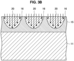
- the exposure device of the manufacturing apparatus radiates the laser light 20 to the resist layer 15 based on the exposure control signal generated in S20 above. Accordingly, the resist layer 15 is exposed in a predetermined exposure pattern to form a latent image 16 corresponding to the object 130.
- the laser light 20 is radiated to the resist layer 15 by the exposure device to denature a portion of the resist layer 15 to which the laser light 20 has been radiated. Accordingly, the resist layer 15 is exposed, and a plurality of latent images 16 are formed on the resist layer 15.
- the laser light as exposure light may be radiated to the resist layer 15 continuously or intermittently. In the case where the laser light 20 is radiated continuously, scanning exposure of continuously radiating the laser light 20 to the surface of the resist layer 15 while relatively moving the laser light 20 in the planar direction of the resist layer 15 may be performed, for example.
- a spot of the laser light 20 may be radiated intermittently to the surface of the resist layer 15 by turning radiation of the laser light 20 on/off while relatively moving the laser light 20 in the planar direction of the resist layer 15, for example.
- continuous radiation or intermittent radiation of the laser light 20 may be selected as appropriate depending on the input image 110.
- the plurality of latent images 16 respectively corresponding to the plurality of objects 130 in the input image 110 are formed on the resist layer 15.
- the three-dimensional shapes of the respective latent images 16 correspond to the three-dimensional shapes of the respective objects 130. Note that specific processing in which the exposure control device generates the exposure control signal based on the input image 110 will be described later.
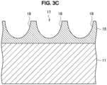
- the development device of the manufacturing apparatus develops the resist layer 15 on which the above-described latent images 16 have been formed. Accordingly, a resist pattern 17 corresponding to the objects 130 is formed on the resist layer 15.
- the development device drops a developing solution onto the resist layer 15 on which the latent images 16 have been formed in S30 above to develop the resist layer 15. Accordingly, the resist pattern 17 having a three-dimensional concave-convex structure is formed on the resist layer 15.
- This resist pattern 17 is composed of a plurality of concavities 18 having a three-dimensional shape.
- the three-dimensional shapes of the plurality of concavities 18 respectively correspond to the three-dimensional shapes of the respective objects 130.
- the depth of the concavity 18 may be such that the deepest portion of the concavity 18 reaches or does not reach the surface of the base member 11.
- the exposed portion exposed to the laser light 20 has a higher rate of dissolution in the developing solution than an unexposed portion and is therefore removed by development treatment. Accordingly, as shown in FIG. 3C , the resist pattern 17 obtained by removing the portions of the latent images 16 in the resist layer 15 is formed on the resist layer 15.
- the resist layer 15 is a negative-type resist
- the exposed portion exposed to the laser light 20 has a lower rate of dissolution in the developing solution than the unexposed portion, so that the unexposed portion is removed by the development treatment. Accordingly, a resist pattern (not shown) in which the portions of the latent images 16 remain is formed on the resist layer 15.
- etching of the base member 11 either dry etching or wet etching can be used.
- the material of the base member 11 is quartz glass (SiO 2 )
- dry etching through use of a fluorocarbon gas (for example, CHF 3 ) or wet etching through use of hydrofluoric acid or the like can be utilized to etch the base member 11.
- the input image 110 in which at least one object 130A, 130B, 130C, 130D (which may hereinafter be collectively referred to as the object 130) having three-dimensional shapes are two-dimensionally drawn is input to the exposure control device.
- the input image 110 is, for example, a rectangular image obtained by opening up the outer circumferential surface of the cylindrical master 1 into a flat surface.
- the input image 110 may be, for example, a grayscale image that two-dimensionally represents the three-dimensional concave-convex structure 13 formed on the outer circumferential surface of the master 1.
- the plurality of objects 130 constituting the plurality of concavities 12 or convexities of the concave-convex structure 13 are expressed two-dimensionally.
- the object 130 is a structural body having any three-dimensional shape (for example, a convex structural body or concave structural body).
- the input image 110 includes a planar image that two-dimensionally expresses the object 130 having the three-dimensional shape.
- the planar shape of the object 130 may be any shape such as, for example, a figure including a curved line, such as a circle or an ellipse, a polygon such as a triangle or a rectangle, a linear shape or a strip shape such as a straight line or a curved line, a shape representing a character or a symbol, or the like.
- the rectangular object 130A, the elliptical object 130B, the pentagonal object 130C, and the triangular object 130D are drawn.
- the input image 110 is an image that expresses a change in height of the three-dimensional shape of the object 130 using a contrasting density of the image.
- the input image 110 preferably is a grayscale image that expresses the change in height of the three-dimensional shape of the object 130 using the contrasting density (that is, levels of grayscale) of the image.
- a lighter colored portion (a region closer to white in grayscale) in the object 130 represents a higher portion of the object 130
- a darker colored portion (a region closer to black in grayscale) in the object 130 represents a lower portion of the object 130.
- some of the small regions, 115B and 115C include the object 130, and other some small regions, 115A, do not include the object 130.
- the contrasting density (the level of grayscale) of the partial image changes in accordance with the height of the three-dimensional shape of the object 130 as compared with the small region 115A not including the object 130.
- the exposure control device analyzes the input image 110 to evaluate whether or not the object 130 is included in each of the small regions 115 of the input image 110. Moreover, as a result of the evaluation, the exposure control device determines that the laser light 20 is to be radiated to the small regions 115B and 115C in which the object 130 is included. On the other hand, the exposure control device determines that the laser light 20 is not to be radiated to the small region 115A in which the object 130 is not included.
- the intensity of the laser light 20 to be radiated to each of the small regions 115 is determined to be a higher intensity.
- the intensity of the laser light 20 to be radiated to each of the small regions 115 is determined to be a lower intensity.
- the exposure control device when evaluating the contrasting density (the level of grayscale) of the partial image in each of the small regions 115 as described above, the exposure control device preferably uses a level corresponding to an average value of the contrasting densities of the partial image in each of the small regions 115 as an evaluation result of the level of grayscale in each of the small regions 115. For example, there are some cases in which the height of the object 130 significantly changes in a certain one of the small regions 115, and the partial image in the one of the small regions 115 has levels of a plurality of grayscales different from each other.
- the exposure device radiates the laser light 20 having the intensity modulated based on the above-described exposure control signal to the resist layer 15. Accordingly, the resist layer 15 is exposed in an exposure pattern corresponding to the above-described exposure control signal.
- the exposure device modulates the intensity of the laser light 20 for each of the small regions 115 in accordance with the contrasting density of the partial image of the object 130 based on the exposure control signal and radiates the modulated laser light 20 to the region corresponding to each of the small regions 115 in the surface of the resist layer 15. Accordingly, the latent image 16 corresponding to the three-dimensional shape of each of the objects 130 is formed on the surface of the resist layer 15 in an exposure pattern corresponding to the plurality of objects 130.
- the development device develops the resist layer 15 after the exposure. Accordingly, the resist pattern 17 corresponding to the three-dimensional shapes of the plurality of objects 130 can be formed on the resist layer 15.
- the depth of the concavity 18 of the resist pattern 17 changes for each of the small regions 115 in the surface of the resist layer 15 in accordance with the contrasting density of the partial image of the above-described object 130.
- the thick resist layer 15 made of an organic resist containing a photosensitive material and having a thickness of several micrometers to several tens of micrometers is used, and the resist layer 15 is exposed through photolithography.
- the organic resist can be deposited more thickly than the inorganic resist.
- a photoreaction of the contained photosensitive material proceeds in reaction in accordance with the light intensity of laser light. Therefore, in the exposure step according to the present embodiment, photolithography through use of the relatively thick resist layer 15 made of the organic resist can be applied to cause the photoreaction of the resist layer 15 at the time of exposure to gradually proceed in the depth direction.
- FIG. 4 is an explanatory diagram showing a general configuration of the exposure device 2 according to the present embodiment.
- the exposure device 2 is a device for exposing the resist layer 15 deposited on the outer circumferential surface of the base member 11 of the roll master 1.
- the exposure device 2 includes a laser light source 21, a laser modulation driver 30, and the formatter 40.
- the laser light source 21 is a light source that emits the laser light 20 and is a solid-state laser, a semiconductor laser, or the like, for example.
- the wavelength of the laser light 20 is not particularly limited and may be a wavelength in a blue light band of 400 nm to 500 nm, for example.
- the laser modulation driver 30 is a driver that controls radiation of the laser light 20 by the laser light source 21.
- the laser modulation driver 30 has a function of modulating the intensity (power) of the laser light 20 to be radiated from the laser light source 21.
- the exposure control signal generated by the above-described formatter 40 is input to the laser modulation driver 30.
- the laser modulation driver 30 modulates the intensity of the laser light 20 to be radiated from the laser light source 21 based on the exposure control signal. As shown in FIG.
- the exposure control signal has a step-like waveform, the signal level of which changes in a stepwise manner in accordance with the contrasting density (the level of grayscale) of the partial image of the object 130 included in each of the small regions 115 of the above-described input image 110.
- the laser modulation driver 30 modulates the intensity of the laser light 20 to be radiated from the laser light source 21 in conformity to the signal level of the exposure control signal having the step-like waveform.
- the laser light 20 the intensity of which has been modulated in accordance with the contrasting density of the partial image of the object 130, is radiated from the laser light source 21 to the base member 11, so that the resist layer 15 is exposed.
- the exposure device 2 having the configuration as described above radiates the laser light 20 to the resist layer 15 of the base member 11 to denature part of the resist layer 15, thereby forming the latent image 16 (see FIG. 3B ).
- the exposure device 2 may, for example, intermittently or continuously radiate the laser light 20 along a spiral track to the resist layer 15 formed on the outer circumferential surface of the cylindrical base member 11 to spirally expose the resist layer 15.
- the exposure device 2 may radiate the laser light 20 to the base member 11 by scanning the base member 11 with the laser light 20 in one direction (R direction) along the central axis 11a of the base member 11 at a constant speed while rotating the base member 11 at a constant speed using the central axis 11a of the cylindrical base member 11 as the rotation axis. Accordingly, the laser light 20 is radiated intermittently or continuously to the surface of the resist layer 15 along the spiral track sequentially from one side to the other side of the base member 11 in the axial direction, and the latent image 16 having a desired shape is formed at a necessary position in the surface of the resist layer 15.
- the laser modulation driver 30 controls radiation of the laser light 20 while modulating the intensity of the laser light 20 based on the exposure control signal generated by the formatter 40. Accordingly, the depth and shape of the resist layer 15 exposed to the laser light 20 can be changed to form the latent image 16 having a three-dimensional shape corresponding to the object 130 on the resist layer 15.
- FIG. 5 is a block diagram showing the configuration of the formatter 40 according to the present embodiment.
- the formatter 40 As shown in FIG. 5 , the formatter 40 according to the present embodiment generates the exposure control signal for controlling radiation of the laser light 20 and a clock signal.
- the formatter 40 includes an input image acquisition unit 401, a small-region division unit 403, a signal generation unit 405, and a clock signal generation unit 407.
- the input image acquisition unit 401 acquires the input image 110 (see FIG. 6 ) in which the object 130 is drawn.
- the input image 110 is, for example, an image equivalent to a developed view obtained by opening up the outer circumferential surface of the cylindrical base member 11 in the axial direction of the base member 11 into a flat surface.
- the planar shape of the object 130 drawn in the input image 110 may be, for example, a figure including a curved line, such as a circle or an ellipse, a polygon such as a triangle or a rectangle, a linear shape or a strip shape such as a straight line or a curved line, a shape representing a character or a symbol, or the like.
- the small-region division unit 403 divides the input image 110 acquired by the input image acquisition unit 401 into the plurality of small regions 115 having a predetermined shape and size. Specifically, the small-region division unit 403 divides the input image 110 into the plurality of small regions 115 at a predetermined lattice interval. For example, as shown in FIG. 6 , the small-region division unit 403 divides the input image 110 at a predetermined interval Px in a direction (the X direction of the input image 110) corresponding to the circumferential direction of the base member 11 and divides the input image 110 at a predetermined interval Py in a direction (the Y direction of the input image 110) corresponding to the axial direction of the base member 11. Note that the interval Px and the interval Py may be the same or different.
- the size (for example, the above-described intervals Px, Py) of the divided small regions 115 preferably is smaller than the size of the spot (for example, the spot diameter) of the laser light 20. Accordingly, the latent images 16 formed by radiation of the laser light 20 can be overlapped on each other without gaps between adjacent ones of the small regions 115. In other words, the exposure device 2 can perform exposure so as to fill in a position corresponding to the object 130 by overlapping a plurality of spots of the laser light 20.
- the intervals Px, Py of the small regions 115 may be 100 nm, and the small regions 115 may be a 100-nm ⁇ 100-nm square.
- the shape of the small regions 115 is not limited to the example of the square and may be any shape such as a rectangular shape, a triangular shape, a polygonal shape, or the like as mentioned above.
- the small-region division unit 403 evaluates whether or not the object 130 is included in each of the small regions 115.
- the small-region division unit 403 also evaluates the degree of the contrasting density (the level of grayscale) of the partial image of the object 130 in each of the small regions 115 in which the object 130 is included.
- FIG. 6 is an explanatory diagram showing the input image 110 divided into the plurality of small regions 115. Note that in FIG. 6 , the X direction corresponds to the circumferential direction of the outer circumferential surface of the base member 11, and the Y direction corresponds to the axial direction of the base member 11.
- the small-region division unit 403 divides the input image 110 including the objects 130A, 130B, 130C, and 130D at the interval Px in the X direction and at the interval Py in the Y direction. Accordingly, the input image 110 is divided into the small regions 115 having a lattice shape.
- the small-region division unit 403 also evaluates whether or not the object 130 is included in each of the small regions 115. For example, the small-region division unit 403 evaluates that the small region 115Ais a small region in which the object 130 is not included and evaluates that the small regions 115B and 115C are small regions in which the object 130 is included.
- the small-region division unit 403 may evaluate that the object is included in the small region 115.
- the small-region division unit 403 may evaluate that the object 130 is included in the small region 115.
- an exposure region 111 may be set in the input image 110 in order to instruct that only some regions of the input image 110 are to be exposed.
- the small-region division unit 403 may evaluate, only for the small regions 115 in the exposure region 111 of the input image 110, whether or not the object 130 is included.
- the signal generation unit 405 generates the exposure control signal for controlling radiation of the laser light 20. Specifically, the signal generation unit 405 determines whether or not to radiate the laser light 20 to a region corresponding to each of the small regions 115 in the resist layer 15 based on an evaluation result of the above-described small-region division unit 403. The signal generation unit 405 further evaluates in a stepwise manner the contrasting density (for example, the level of grayscale) of the partial image of the object 130 in each of the small regions 115 in which the object 130 is included. Then, based on the evaluation result, the signal generation unit 405 determines in a stepwise manner the intensity of the laser light 20 to be radiated to each of the small regions 115.
- the contrasting density for example, the level of grayscale
- the signal generation unit 405 further generates an exposure control signal indicating the intensity and timing of the laser light 20 to be radiated to each of the small regions 115 based on the evaluation result (for example, data representing the intensity of the laser light 20 to be radiated to each of the small regions 115).
- the signal generation unit 405 converts the data representing the intensity of the laser light 20 determined as described above into the exposure control signal using the clock signal generated by the clock signal generation unit 407.
- the exposure control signal thus generated by the signal generation unit 405 is transmitted to the driver 30 that controls the laser light source 21.
- the driver 30 controls radiation of the laser light 20 by the laser light source 21 based on the exposure control signal.
- FIG. 7 is an explanatory diagram showing a specific example of the exposure control signal corresponding to a surrounding image of the object 130A in the input image 110 shown in FIG. 6 .
- the signal generation unit 405 evaluates, for each row in the X direction of the input image 110, the contrasting density (for example, the level of grayscale) of the partial image in each of the small regions 115 and based on the evaluation result, determines the intensity of the laser light 20 to be radiated to each of the small regions 115.
- the contrasting density for example, the level of grayscale
- the signal generation unit 405 first selects the uppermost row of the input image 110 (or the exposure region 111) and evaluates the contrasting density (for example, the level of grayscale) of the partial image in each of the small regions 115 successively from the leftmost small region 115 to the rightmost small region 115 in this row (that is, in the positive direction of the X axis).
- the contrasting density for example, the level of grayscale
- the signal generation unit 405 assigns "0" as the level of grayscale to the small regions 115 in which the object 130 is not included.
- the signal generation unit 405 assigns, to the small regions 115 in which the object 130 is included, numeric values (for example, in the example of FIG. 7 , twenty-four levels of "0 to 23") of the levels of grayscale in accordance with the contrasting density of the partial image of the object 130 in the small regions 115. Accordingly, the signal generation unit 405 evaluates the level of grayscale of each of the small regions 115 successively from the leftmost small region 115 to the rightmost small region 115 in one row.
- the signal generation unit 405 selects an immediately underlying subsequent row and performs processing similar to the foregoing in that row to evaluate the level of grayscale of each of the small regions 115 in that row.
- the signal generation unit 405 further repeats this evaluation processing successively from an upper row to a lower row (in the negative direction of the Y direction), thereby evaluating the levels of grayscale of the plurality of small regions 115 in the entire region of the input image 110 (or the exposure region 111).
- the order in which the signal generation unit 405 evaluates the levels of grayscale in each row in the X direction of the input image 110 is set based on a direction in which the base member 11 rotates.
- the signal generation unit 405 may evaluate the levels of grayscale successively from the rightmost small region 115 to the leftmost small region 115 (in the negative direction of the X axis) for each row in the X direction depending on the direction in which the base member 11 rotates.
- the order in which the signal generation unit 405 evaluates the levels of grayscale in the Y direction of the input image 110 is set based on a direction in which the base member 11 is scanned with the laser light 20.
- the signal generation unit 405 may evaluate the levels of grayscale successively from a lower row to an upper row of the input image 110 (in the positive direction of the Y axis) depending on the direction in which the base member 11 is scanned with the laser light 20.
- the signal generation unit 405 converts data representing the above-described evaluation result of the level of grayscale of each of the small regions 115 (equivalent to the data representing the intensity of the laser light 20 to be radiated to each of the small regions 115) into the exposure control signal using the clock signal acquired from the clock signal generation unit 407.
- the clock signal is a rectangular wave signal having a predetermined frequency.
- the data representing the evaluation result of the level of grayscale is, for example, numeric value data representing the level of grayscale assigned to each of the small regions 115 of the input image 110.
- the exposure control signal is a signal having a step-like waveform.
- the signal level of the exposure control signal increases/decreases in a stepwise manner in accordance with the level of grayscale representing the contrasting density of the partial image in each of the small regions 115.
- the exposure control signal has the highest signal level.
- the signal generation unit 405 generates the exposure control signal in synchronization with the clock signal.
- the exposure control signal is generated such that rise and fall times of the exposure control signal coincide with either a rise time or a fall time of the clock signal.
- the exposure control signal is generated such that the rise and fall of the exposure control signal coincide with the rise of the clock signal.
- the clock signal generation unit 407 generates a clock signal to be a reference of the exposure control signal. Specifically, the clock signal generation unit 407 acquires, from a spindle motor 35 that rotates the base member 11, a rotation control signal for controlling rotation of the spindle motor 35 and generates a clock signal having a predetermined frequency based on the rotation control signal.
- the rotating speed of the spindle motor 35 that rotates the base member 11 is not constant all the time and fluctuates even in a case where a constant rotating speed is set.
- the rotation control signal that controls rotation of the spindle motor 35 and the exposure control signal that controls radiation of the laser light 20 are not in synchronization, one rotation of the spindle motor 35 and one period of the exposure control signal might not coincide with each other.
- the position of the outer circumferential surface of the base member 11 to which the laser light 20 is radiated is offset per rotation of the base member 11, so that the concave-convex pattern corresponding to the object 130 might not be formed at an accurate position on the outer circumferential surface of the base member 11.
- the exposure device 2 generates the clock signal from the rotation control signal for controlling rotation of the spindle motor 35 and based on the clock signal, generates the exposure control signal for controlling radiation of the laser light 20, as mentioned above. Accordingly, the rotation control signal and the exposure control signal are brought into synchronization. Therefore, the position of the outer circumferential surface of the base member 11 to which the laser light 20 is to be radiated is not offset per rotation of the base member 11, which enables the concave-convex pattern corresponding to the object 130 to be formed at an accurate position on the outer circumferential surface of the base member 11.
- a method for bringing the rotation control signal and the exposure control signal into synchronization is not limited to the above-described example.
- the clock signal generation unit 407 may transmit the clock signal to be the reference to the spindle motor 35 and the signal generation unit 405, respectively.
- the spindle motor 35 generates the rotation control signal that controls rotation of the spindle motor 35 based on the clock signal
- the signal generation unit 405 generates the exposure control signal based on the clock signal.
- This method can also bring the rotation control signal that controls rotation of the spindle motor 35 and the exposure control signal that controls radiation of the laser light 20 into synchronization.
- the functional configuration of the formatter 40 that generates the exposure control signal that controls radiation of the laser light 20 has been described above.
- This formatter 40 enables the exposure control signal corresponding to the three-dimensional shape of any object 130 to be suitably generated.
- the function of this formatter 40 is achieved by cooperation of software and hardware.
- the formatter 40 may include a CPU (Central Processing Unit), a ROM (Read Only Memory), a RAM (Random Access Memory), and the like connected to one another with a bridge to achieve the above-described function by these types of hardware.
- a CPU Central Processing Unit
- ROM Read Only Memory
- RAM Random Access Memory
- the CPU functions as an arithmetic processing unit and a control device to control overall operation in the formatter 40 in accordance with various programs.
- the ROM stores programs to be used by the CPU and arithmetic parameters
- the RAM temporarily stores programs to be used in execution of the CPU, parameters that vary as appropriate in execution thereof, and the like. Accordingly, the CPU can execute the functions of the input image acquisition unit 401, the small-region division unit 403, the signal generation unit 405, and the clock signal generation unit 407, for example.
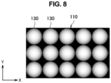
- FIG. 8 is an explanatory diagram showing a specific example of the input image 110 according to the present embodiment.
- FIG. 9 is an explanatory diagram showing a specific example of the input image 110 divided into the plurality of small regions 115 and the contrasting density (the level of grayscale) of the partial image of the object 130.
- FIG. 10 is an explanatory diagram showing a specific example of the exposure control signal corresponding to a partial image of one of the objects 130 (microlenses) of the input image 110 shown in FIG. 9 .
- the input image 110 is divided into the plurality of small regions 115, and the exposure control signal is generated based on the contrasting density (the level of grayscale) of the partial image of each of the small regions 115, similarly to the above-mentioned specific example of FIGS. 6 and 7 .
- the contrasting density the level of grayscale
- the input image 110 may be a grayscale image in which the plurality of objects 130 having the same shape are drawn.
- the input image 110 in the example of FIG. 8 represents a microlens array, and an individual microlens is equivalent to the object 130.
- a plurality of microlenses are regularly arrayed as the objects 130 vertically and laterally (in the X and Y directions) in a square lattice shape.
- the plurality of microlenses are arranged at intervals from one another.
- the input image 110 shown at the upper side in FIG. 9 is obtained by cutting a partial image of five microlenses (the objects 130) arrayed in the central row in the Y direction out of the input image 110 in FIG. 8 .
- the input image 110 is divided into the plurality of small regions 115 by square lattice-shaped grid lines.
- the interval Px between the grid lines in the X direction and the interval Py between the grid lines in the Y direction are equal, and the small region 115 is a square grid.
- the present invention is not limited to such an example, and for example, the interval Px and the interval Py may be different from each other, and the small region 115 may be a grid having a rectangular shape or another shape.
- a region of the input image 110 in which one microlens (the object 130) is present preferably is divided into a large number of, for example, more than or equal to one hundred small regions 115 in accordance with the difference in height of the three-dimensional shape of the microlens (divided into ten or more small regions in the X direction and divided into ten or more small regions in the Y direction, for example). Accordingly, the three-dimensional spherical or aspherical shape of the individual microlens can be reproduced precisely and smoothly on the outer circumferential surface of the base member 11 of the master 1 using the partial image of the large number of small regions 115.
- a bar graph shown at the lower side in FIG. 9 shows a change in the contrasting density (for example, the level of grayscale) of the partial image of one row that transverses five microlenses in the X direction substantially at the center in the Y direction in the input image 110 at the upper side in FIG. 9 .
- the contrasting density of the partial image of each of the small regions 115 is obtained. Accordingly, the change in height of the three-dimensional shape of the microlens two-dimensionally drawn in the input image 110 can be adequately recognized and reflected in the exposure control signal. Therefore, as shown in FIG. 10 , the exposure control signal corresponding to the three-dimensional shape of the microlens can be generated from the contrasting density (the level of grayscale) of the partial image of each of the small regions 115.
- the exposure control signal shown in FIG. 10 has a step-like waveform in accordance with the level of grayscale representing the contrasting density of the partial image of the microlens (the object 130) similarly to the exposure control signal in the above-mentioned example of FIG. 7 .
- the signal level of the exposure control signal is set at a higher value.
- the change in the signal level of the exposure control signal corresponds to the change in height of the three-dimensional shape of one microlens.
- the master 1 for manufacturing the microlens array drawn in the input image 110 can be manufactured.
- the concave-convex structure 13 corresponding to the three-dimensional shape of the microlens array two-dimensionally drawn in the input image 110 shown in FIG. 8 for example, can be reproduced on the outer circumferential surface of the master 1 with high accuracy.
- the product targeted to be manufactured with the master 1 is not limited to the example of the microlens array shown in FIG. 8 and the like described above, and the present invention can be applied to various products.
- the product targeted to be manufactured with the master 1 may be a microlens array in which a plurality of microlenses are irregularly arranged or may be an antireflection film, a diffuser panel, a polarizer, a diffraction grating, other various optical members, or the like on which a moth-eye structure having a concave-convex period of less than or equal to a wavelength belonging to a visible light band has been formed.
- the input image 110 in which a desired concave-convex structure formed on these various optical members is drawn as the object 130 in grayscale may be generated, and the input image 110 may be applied to the method for manufacturing the master 1 according to the present embodiment. Accordingly, the master 1 to be used for manufacturing products of an optical member having the desired concave-convex structure can be manufactured easily with high accuracy.
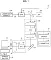
- FIG. 11 is an explanatory diagram showing a configuration example of an exposure device 2A according to the present embodiment.
- FIG. 12 is an explanatory diagram showing another configuration example of an exposure device 2B according to the present embodiment.
- the exposure device 2A is an exposure device that uses a solid-state laser as a laser light source 21A.
- the exposure device 2A includes the laser light source 21A, an electro optical modulator (EOM) 22, a first mirror 23, a photodiode (PD) 24, a modulation optical system 25, a control mechanism 37, a second mirror 31, a moving optical table 32, the spindle motor 35, and a turntable 36.
- EOM electro optical modulator
- PD photodiode
- modulation optical system 25
- control mechanism 37 a control mechanism 37
- the base member 11 is placed on the turntable 36 and is capable of rotating.
- the laser light source 21A is specifically a solid-state laser.
- a solid-state laser or the like having a wavelength of 266 nm can be used as the laser light source 21A.
- the laser light 20 exited from the laser light source 21A travels straight as a parallel beam and enters the electro optical modulator 22.
- the laser light 20 transmitted through the electro optical modulator 22 is reflected off the first mirror 23 and guided to the modulation optical system 25.
- the first mirror 23 is composed of a polarization beam splitter and has a function of reflecting one of polarization elements and transmitting the other of the polarization elements.
- the polarization element transmitted through the first mirror 23 is received by the photodiode 24 and subjected to photoelectric conversion.
- a light reception signal obtained by the photoelectric conversion by the photodiode 24 is input to the electro optical modulator 22.
- the electro optical modulator 22 performs phase modulation of the laser light 20 based on the input light reception signal.
- the modulation optical system 25 includes a condenser lens 26, an acousto-optic modulator (AOM) 27, and a collimator lens 28.
- AOM acousto-optic modulator
- the laser light 20 is condensed onto the acousto-optic modulator 27 formed from glass (SiO 2 ) and the like by the condenser lens 26.
- the laser light 20 is modulated in intensity by the acousto-optic modulator 27 and diffuses, and is then rendered into a parallel beam again by the collimator lens 28.
- the laser light 20 exited from the modulation optical system 25 is reflected off the second mirror 31 and guided onto the moving optical table 32 horizontally and in parallel.
- control mechanism 37 includes the formatter 40 and the driver 30 and controls radiation of the laser light 20.
- the formatter 40 generates the exposure control signal for controlling radiation of the laser light 20 as mentioned above, and the driver 30 controls the acousto-optic modulator 27 based on the exposure control signal generated by the formatter 40. Accordingly, radiation of the laser light 20 to the resist layer 15 is controlled.
- the moving optical table 32 includes a beam expander (BEX) 33 and an objective lens 34.
- BEX beam expander
- the laser light 20 guided to the moving optical table 32 is shaped into a desired beam shape by the beam expander 33 and then radiated to the resist layer 15 on the outer circumferential surface of the base member 11 through the objective lens 34.
- the exposure device 2A preferably is subjected to focus control dynamically such that the laser light 20 is always focused on the resist layer 15 on the base member 11.
- the distance from the objective lens 34 to the base member 11 varies during rotation due to axis offset of the rotation axis, processing accuracy of the surface of the base member 11, and the like.
- the exposure device 2A preferably detects a focus shift of the laser light 20 and dynamically control focusing of the laser light 20.
- a method for detecting the focus shift of the laser light 20 with respect to the resist layer 15 on the base member 11 a method for detecting astigmatism of reflected light of the laser light 20 radiated to the resist layer 15, or the like can be used, for example.
- the base member 11 is rotated by the turntable 36 at a constant speed and the laser light 20 is radiated while scanning the base member 11 in the axial direction at a constant speed, thereby exposing the resist layer 15.
- scanning with the laser light 20 is performed by moving the laser light 20 by the moving optical table 32 in the direction of an arrow R at a constant speed.
- the rotation control signal for controlling rotation of the spindle motor 35 and the exposure control signal for controlling radiation of the laser light 20 are in synchronization such that actual radiated positions of the laser light 20 and radiated positions indicated by the exposure control signal conform (synchronize). Accordingly, the exposure device 2A can expose the resist layer 15 without the radiated position of the laser light 20 being shifted per rotation of the base member 11.
- the rotating speed of the turntable 36 of the exposure device 2A and the frequency of the exposure control signal generated by the formatter 40 are determined by the outer circumferential length of the cylindrical shape of the base member 11 and the division interval Px in the circumferential direction (the X direction) of the input image 110.
- a feed pitch of the moving optical table 32 of the exposure device 2A is determined by the division interval Py in the axial direction (the Y direction) of the input image 110.
- the exposure device 2B includes the laser light source 21B, the first mirror 23, the photodiode (PD) 24, the condenser lens 26, an electro optic deflector (EOD) 29, the collimator lens 28, the control mechanism 37, the second mirror 31, the moving optical table 32, the spindle motor 35, and the turntable 36.
- the base member 11 is placed on the turntable 36 and is capable of rotating.
- the laser light source 21B specifically is a semiconductor laser.
- a blue semiconductor laser that emits laser light having a wavelength in the blue light band of 400 nm to 500 nm can be used as the laser light source 21B.
- a semiconductor laser preferably is used as the laser light source 21B.
- the laser light 20 exited from the laser light source 21B travels straight as a parallel beam and is reflected off the first mirror 23.
- the laser light 20 reflected off the first mirror 23 is condensed onto the electro optic deflector 29 by the condenser lens 26, and is then rendered into a parallel beam again by the collimator lens 28.
- the laser light 20 rendered into the parallel beam is reflected off the second mirror 31 and guided onto the moving optical table 32 horizontally and in parallel.
- the first mirror 23 is composed of a polarization beam splitter and has a function of reflecting one of polarization elements and transmitting the other of the polarization elements.
- the polarization element transmitted through the first mirror 23 is received by the photodiode 24 and subjected to photoelectric conversion.
- a light reception signal obtained by the photoelectric conversion by the photodiode 24 is input to the laser light source 21B.
- the laser light source 21B modulates the laser light 20 based on the input light reception signal.
- the electro optic deflector 29 is an element capable of controlling radiated positions of the laser light 20.
- the exposure device 2B is also capable of changing the radiated positions of the laser light 20 to be guided onto the moving optical table 32 by the electro optic deflector 29.
- control mechanism 37 includes the formatter 40 and the driver 30 and controls radiation of the laser light 20.
- the driver 30 controls output of the laser light source 21B based on the exposure control signal generated by the formatter 40. Accordingly, radiation of the laser light 20 to the resist layer 15 is controlled.
- the exposure device 2B shown in FIG. 12 dynamically controls focus of the laser light 20 and brings the rotation control signal for the spindle motor 35 and the exposure control signal for the laser light 20 into synchronization, similarly to the exposure device 2A shown in FIG. 11 .
- the intensity of the laser light 20 is modulated in accordance with the contrasting density (for example, the level of grayscale) of the image of the object 130 drawn in any input image 110, and the resist layer 15 on the outer circumferential surface of the base member 11 is exposed using the laser light 20 modulated in intensity.
- the resist pattern 17 corresponding to any three-dimensional shape of the object 130 can be formed on the resist layer 15.
- the concave-convex structure 13 corresponding to the three-dimensional shape can be formed on the outer circumferential surface of the base member 11.
- a pattern of the concave-convex structure 13 corresponding to the object 130 having any three-dimensional shape can be formed on the outer circumferential surface of the base member 11 of the master 1 at a higher accuracy than in the conventional art.
- the grid lines for dividing the input image 110 into the plurality of small regions 115 can be freely set regardless of the arrangement and the concave-convex shape of the objects 130 in the input image 110. Since the flexibility of the method for dividing the input image 110 into the small regions 115 is high as described, the exposure control signal flexibly corresponding to the arrangement and the concave-convex shape of the object 130 can be generated and utilized for exposure of the resist layer 15. Thus, the concave-convex structure 13 corresponding to the object 130 having any three-dimensional shape can be freely formed on the outer circumferential surface of the master 1.
- Patent Literature 1 performs scanning exposure of relatively moving exposure light in the planar direction of the resist film for continuous radiation rather than intermittently radiating a spot of laser light modulated in intensity in accordance with the input image 110 as exposure light.
- continuous scanning exposure raises a problem in that it is difficult to form a pattern of a concave-convex structure having a desired three-dimensional shape with high accuracy.
- a spot of the laser light 20 modulated in intensity in accordance with the contrasting density of the input image 110 is used as exposure light, and the spot of the laser light 20 is radiated intermittently or continuously to each of regions of the resist layer 15 corresponding to the small regions 115 of the input image 110.
- the spot of the laser light 20 modulated in intensity is radiated to each of the regions of the resist layer 15 corresponding to the small regions 115 while modulating the intensity of the laser light 20 for each of the small regions 115 of the input image 110.
- the size (such as, for example, the area or the intervals Px, Pc) of the small regions 115 preferably is smaller than the size (such as, for example, the radiated area or spot diameter) of the spot of the laser light 20 to be radiated to the resist layer 15.
- the resist layer 15 can be suitably exposed to a desired depth, into a desired three-dimensional shape, and in a desired arrangement in conformity to the height, three-dimensional shape, and arrangement of the objects 130 drawn in the input image 110. Therefore, the resist pattern 17 composed of the plurality of latent images 16 corresponding to the objects 130 can be formed with high accuracy and freely.
- the pattern of the concave-convex structure 13 having a desired three-dimensional shape can be formed with high accuracy and freely on the outer circumferential surface of the base member 11 of the master 1 using the resist pattern 17.
- the intensity of the laser light 20 to be radiated to the resist layer 15 can be freely modulated in conformity to the contrasting density (for example, the level of grayscale) of the partial image of the object 130 in the input image 110. Therefore, the resist pattern 17 having a desired three-dimensional shape can be formed appropriately when the resist layer 15 is exposed.
- the depth, three-dimensional shape, and arrangement of the micro concave-convex structure 13 formed on the outer circumferential surface of the master 1 using the resist pattern 17 can be freely changed in conformity to the pattern of the three-dimensional shape of the desired object 130.
- the master 1 manufactured by the manufacturing method according to the present embodiment is a roll master having a cylindrical shape or a columnar shape and has the concave-convex structure 13 having any three-dimensional shape formed on its outer circumferential surface.
- the three-dimensional shape of the concave-convex structure 13 may be various shapes corresponding to any object 130 as shown in FIGS. 1 and 6 , for example, or may be a concave-convex shape of an optical member such as a microlens array in which a plurality of microlenses (an individual microlens of which is an example of the object 130) are arrayed regularly or irregularly as shown in FIGS. 8 and 9 .
- the transferred object By manufacturing the transferred object using this roll master 1, the productivity and quality of the transferred object (for example, an optical sheet on which a microlens array has been formed) having a surface to which the concave-convex structure 13 having any three-dimensional shape as described above has been transferred can be improved. Furthermore, in the present embodiment, the transferred object is manufactured in the roll-to-roll system using the manufacturing apparatus including the roll master 1. Accordingly, a product including a micro concave-convex structure such as a microlens array can be manufactured more inexpensively and with higher productivity than conventional manufacturing apparatuses including a planar master.
- the masters 1 and the transferred objects according to Examples 1 to 4 of the present invention were manufactured by the following manufacturing methods.
- the resist layer 15 having a thickness of 10 ⁇ m was formed on the outer circumferential surface of the cylindrical base member 11 by a dip coating method.
- the base member 11 a base member made of cylindrical quartz glass having a thickness of 4.5 mm was used.
- a positive-type photoresist for example, the product name: "AZ-P4210” made by Merck & Co., Inc.
- the exposure control signal was generated using the input image 110.
- the input image 110 an exposure pattern
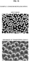
- a grayscale image of a microlens array in which a plurality of microlenses (equivalent to the objects 130) having the same shape were arrayed regularly in a square lattice shape was used as shown in FIG. 13 .
- the microlenses having a diameter of 20 ⁇ m and a height of 4 ⁇ m were aligned at a pitch of 20 ⁇ m substantially without gaps between one another.
- the intervals Px, Py at which the input image 110 was divided into the plurality of small regions 115 was set at 200 nm.
- the levels of grayscale indicating the contrasting density of the partial image of the microlenses were set at 256 levels.
- the resist layer 15 deposited on the outer circumferential surface of the base member 11 was exposed while modulating the intensity of the laser light 20 based on the exposure control signal.
- the latent image 16 was formed on the resist layer 15 of the base member 11 using the exposure device 2B shown in FIG. 12 through photolithography with the laser light 20.
- a blue semiconductor laser that emits the laser light 20 having a wavelength of 405 nm was used as the laser light source 21B of the exposure device 2B.
- the base member 11 was scanned with the laser light 20 in the axial direction of the base member 11 at 1.5 ⁇ m/sec at the time of exposure while rotating the base member 11 around the central axis 11a at 900 rpm.
- the base member 11 after the above-described exposure was developed.
- the base member 11 was developed at 27°C for 1800 seconds using a 2.38 mass % aqueous solution of TMAH to dissolve resist in an exposed portion, thereby forming the resist pattern 17.
- the base member 11 was dry-etched using the resist pattern 17 after the above-described development as a mask.
- reactive ion etching was performed using a CHF 3 gas (flow rate: 30 sccm) as an etching gas at a gas pressure of 0.5 Pa in a chamber, at applied RF power of 150W for an etching time of 300 minutes.
- the concave-convex structure 13 was formed on the outer circumferential surface of the base member 11.
- the master 1 according to Example 1 was manufactured through the above steps. Furthermore, the transferred object according to Example 1 was manufactured using the manufactured master 1. Specifically, the resin layer 62 made of an ultraviolet curing resin was laminated on a surface of a sheet-like base member (the to-be-transferred object 61) of the transferred object using the transfer device 6 as shown in FIG. 2 , and the concave-convex structure 13 formed on the outer circumferential surface of the master 1 was transferred to the resin layer 62 yet to be cured. Note that a polyethylene terephthalate (PET) film was used for the sheet-like base member of the transferred object.
- PET polyethylene terephthalate
- the transferred object (a product of the microlens array) in which the concave-convex structure 13 of the master 1 has been transferred to the resin layer 62 was manufactured.
- FIG. 13 An SEM image of the aligned microlens array which is the transferred object according to Example 1 manufactured as described above is shown at the lower side of FIG. 13 . As shown in FIG. 13 , it is found that in the aligned microlens array according to Example 1, the three-dimensional shape of the microlens array composed of the plurality of microlenses (the objects 130) drawn in the input image 110 has been reproduced with high accuracy on a surface of the transferred object.
- Example 2 the method for manufacturing the master 1 and the transferred object according to Example 2 will be described.
- the master 1 and the transferred object were manufactured by a manufacturing method similar to that of Example 1 except for the input image 110 to be used in the exposure control signal generation step (S20).
- Example 2 the input image 110 for manufacturing an aligned microlens array in which microlenses were arrayed at an array pitch larger than in Example 1 ( FIG. 13 ) was used.
- a grayscale image of a microlens array in which a plurality of microlenses (equivalent to the objects 130) having the same shape were arrayed regularly in a square lattice shape was used as shown in FIG. 14 .
- the microlenses having a diameter of 25 ⁇ m and a height of 3 ⁇ m were aligned at a pitch of 25 ⁇ m at intervals from one another.
- the intervals Px, Py at which the input image 110 was divided into the plurality of small regions 115 were set at 200 nm.
- the levels of grayscale indicating the contrasting density of the partial image of the microlenses were set at 256 levels.
- FIG. 14 An SEM image of the aligned microlens array as the transferred object according to Example 2 is shown at the lower side of FIG. 14 .
- FIG. 14 it is found that, also in the aligned microlens array according to Example 2, the three-dimensional shape of the microlens array composed of the plurality of microlenses (the objects 130) drawn in the input image 110 has been reproduced on a surface of the transferred object with high accuracy.
- Example 3 the method for manufacturing the master 1 and the transferred object according to Example 3 will be described.
- the master 1 and the transferred object were manufactured by a manufacturing method similar to that of Example 1 except for the input image 110 to be used in the exposure control signal generation step (S20).
- Example 3 the input image 110 for manufacturing a random microlens array in which a plurality of microlenses were irregularly arranged was used.
- a grayscale image of a microlens array in which a plurality of microlenses (equivalent to the objects 130) having substantially the same shape were arranged at random was used as shown in FIG. 15 .
- the microlenses generally having a diameter of 10 ⁇ m and a height of 3 ⁇ m were arranged at random dispersedly to some degree.
- the intervals Px, Py at which the input image 110 was divided into the plurality of small regions 115 were set at 200 nm.
- the levels of grayscale indicating the contrasting density of the partial image of the microlenses were set at 256 levels.
- FIG. 15 An SEM image of the random microlens array as the transferred object according to Example 3 is shown at the lower side of FIG. 15 . As shown in FIG. 15 , it is found that in the random microlens array according to Example 3, the three-dimensional shape of the microlens array composed of the plurality of microlenses (the objects 130) drawn in the input image 110 has been reproduced on a surface of the transferred object with high accuracy.
- Example 4 the method for manufacturing the master 1 and the transferred object according to Example 4 will be described.
- the master 1 and the transferred object were manufactured by a manufacturing method similar to that of Example 1 except for the input image 110 to be used in the exposure control signal generation step (S20).
- Example 4 the input image 110 for manufacturing a random microlens array in which a larger number of microlenses were arranged densely and irregularly than in Example 3 ( FIG. 15 ) was used.
- a grayscale image of a microlens array in which a plurality of microlenses (equivalent to the objects 130) having shapes different from each other were arranged at random as shown in FIG. 16 was used.
- the microlenses generally having a diameter of 10 ⁇ m and a height of 2 ⁇ m were arranged densely without gaps between one another and at random.
- the intervals Px, Py at which the input image 110 was divided into the plurality of small regions 115 were set at 200 nm.
- the levels of the grayscale image indicating the contrasting density of the partial image of the microlenses were set at 256 levels.
- FIG. 16 An SEM image of the random microlens array as the transferred object according to Example 4 is shown at the lower side of FIG. 16 . As shown in FIG. 16 , it is found that, also in the random microlens array according to Example 4, the three-dimensional shape of the microlens array composed of the plurality of microlenses (the objects 130) drawn in the input image 110 has been reproduced on a surface of the transferred object with high accuracy.
- Examples 1 to 4 confirmed that the pattern of the micro concave-convex structure 13 of the microlens array having any three-dimensional shape was able to be formed with high accuracy on the outer circumferential surface of the master 1 by the method for manufacturing the master according to the present embodiment. It was also confirmed that the concave-convex structure 13 of the master 1 was able to be transferred to the transferred object with high accuracy by the method for manufacturing the transferred object through use of the master 1, enabling products of various microlens arrays to be mass-produced inexpensively and efficiently.
- the master 1 and the transferred object thereof manufactured by the manufacturing method according to the present embodiment can suitably achieve a concave-convex structure having any three-dimensional shape and thus can be applied to various applications.
- the transferred object can be applied to the printed electronics by forming a circuit on the transferred concave-convex structure.
- the transferred object can be applied to a biosensor or diagnostic device by forming a flow passage of a biological sample such as the blood in the transferred concave-convex structure.
- the transferred object can also be applied to an optical element by controlling optical characteristics by the transferred concave-convex structure.
- the transferred object can be applied to a particle array sheet by using the transferred concave-convex structure.
Landscapes
- Physics & Mathematics (AREA)
- General Physics & Mathematics (AREA)
- Engineering & Computer Science (AREA)
- Mechanical Engineering (AREA)
- Optics & Photonics (AREA)
- Manufacturing & Machinery (AREA)
- Exposure And Positioning Against Photoresist Photosensitive Materials (AREA)
- Shaping Of Tube Ends By Bending Or Straightening (AREA)
- Moulds For Moulding Plastics Or The Like (AREA)
Abstract
Description
- The present invention relates to a method for manufacturing a master, a method for manufacturing a transferred object and a replica master through use of a master, as well as an apparatus for manufacturing a master.
- In recent years, the development of a nanoimprinting technology of pressing a planar or columnar master having a micro concave-convex pattern formed on its surface against a resin sheet or the like to transfer the micro concave-convex pattern on the master to the resin sheet or the like has been advanced as one of microfabrication technologies. In a case of manufacturing such a master for imprinting, a lithography technology through use of exposure with laser light is used.
- For example,
Patent Literature 1 discloses a technology for forming a concave-convex structure of microlenses on a surface of a planar die master through lithography with laser light. - In addition,
Patent Literature 2 discloses a technology for forming a pattern of a concave-convex structure (for example, a moth-eye structure having a concave-convex period of less than or equal to a wavelength belonging to a visible light band) on an outer circumferential surface of a cylindrical or columnar roll master through thermal lithography with laser light and transferring the pattern of the concave-convex structure on the outer circumferential surface of the roll master to a resin sheet. -
Patent Literature 1: JP 2018-165811A Patent Literature 2: JP 2016-028867A - However, in the technology described in
Patent Literature 1 above, when a resist film on the surface of the planar die master is exposed with laser light, exposure is performed for each of sectioned exposure target regions. The exposure target regions are sectioned by boundary portions between concavities in which exposure light has a small intensity and an exposure depth is shallow. This raises a problem in that a concave-convex structure having any three-dimensional shape in which concave-convex structures of adjacent sections are coupled continuously and seamlessly cannot be freely formed. - In addition, in the technology described in
Patent Literature 2, the intensity of laser light is not modulated when the resist layer on the outer circumferential surface of the roll master is exposed, and the concave-convex pattern is exposed by turning on/off laser light having a constant intensity. Thus, only an exposure pattern having a constant depth can be formed on the resist layer. Therefore, a problem arises in that it is difficult to freely form a concave-convex structure having any three-dimensional shape by arbitrarily varying the depth of the pattern of the concave-convex structure. - The present invention was therefore made in view of the above problems, and an object of the present invention is to form a pattern of a concave-convex structure having any three-dimensional shape on an outer circumferential surface of a master with high accuracy.
- In order to solve the above-described problems, according to a certain aspect of the present invention, provided is a method for manufacturing a master, including the steps of forming a resist layer on an outer circumferential surface of a base member having a cylindrical shape or a columnar shape, dividing an input image in which at least one object having a three-dimensional shape is two-dimensionally drawn into a plurality of small regions, determining whether or not to radiate laser light to each of the small regions based on whether or not the object is included in each of the small regions, determining in a stepwise manner an intensity of the laser light to be radiated to each of the small regions based on a contrasting density of a partial image of the object in each of the small regions in which the object is included, and generating an exposure control signal corresponding to the object based on a result of the determining of the intensity of the laser light, radiating, to the resist layer, the laser light modulated in the intensity in accordance with the contrasting density of the partial image of the object for each of the small regions based on the exposure control signal, thereby forming a resist pattern corresponding to the object on the resist layer, and forming a concave-convex pattern corresponding to the three-dimensional shape of the object on the outer circumferential surface of the base member using, as a mask, the resist layer on which the resist pattern has been formed. In the resist pattern, the resist pattern changes in depth in each of the small regions in accordance with the contrasting density of the partial image of the object.
- The input image may be a grayscale image that expresses a change in height of the three-dimensional shape of the object using the contrasting density of the grayscale image. In the step of generating the exposure control signal, the intensity of the laser light to be radiated to each of the small regions may be determined in a stepwise manner based on a level of a grayscale of the partial image of the object in each of the small regions in which the object is included.
- The exposure control signal may be a modulation signal for modulating in a stepwise manner the intensity of the laser light that exposes the resist layer and may have a step-like waveform in accordance with a level of a grayscale that represents the contrasting density of the partial image of the object.
- The small regions may each have a size smaller than a size of a spot of the laser light.
- In the step of forming the resist pattern on the resist layer, the laser light may be radiated to the resist layer of the base member while the base member is rotated using a central axis of the base member as a rotation axis.
- The exposure control signal may be generated so as to be synchronized with a signal for controlling rotation of the base member.
- A light source of the laser light may be a semiconductor laser, the resist layer may be made of an organic resist, and in the step of forming the resist pattern on the resist layer, the resist pattern may be formed on the resist layer through photolithography.
- In order to solve the above-described problems, according to another aspect of the present invention, provided is a method for manufacturing a transferred object, including the step of transferring a pattern of the master manufactured by the method for manufacturing the master.
- In order to solve the above-described problems, according to another aspect of the present invention, provided is a method for manufacturing a replica master, including the step of transferring a pattern of the transferred object manufactured by the method for manufacturing a transferred object.
- In order to solve the above-described problems, according to another aspect of the present invention, provided is a method for manufacturing a transferred object, including the step of transferring a pattern of the replica master manufactured by the manufacturing method according to claim 9.
- In order to solve the above-described problems, according to another aspect of the present invention, provided is an apparatus for manufacturing a master, including a deposition device that forms a resist layer on an outer circumferential surface of a base member having a cylindrical shape or a columnar shape, an exposure control device that divides an input image in which at least one object having a three-dimensional shape is two-dimensionally drawn into a plurality of small regions, makes a determination as to whether or not to radiate laser light to each of the small regions based on whether or not the object is included in each of the small regions, makes a determination in a stepwise manner as to an intensity of the laser light to be radiated to each of the small regions based on a contrasting density of a partial image of the object in each of the small regions in which the object is included, and generates an exposure control signal corresponding to the object based on a result of the determination of the intensity of the laser light, an exposure device that radiates, to the resist layer, the laser light modulated in the intensity in accordance with the contrasting density of the partial image of the object for each of the small regions based on the exposure control signal, thereby forming a resist pattern corresponding to the object on the resist layer, and an etching device that forms a concave-convex pattern corresponding to the three-dimensional shape of the object on the outer circumferential surface of the base member using, as a mask, the resist layer on which the resist pattern has been formed. In the resist pattern, the resist pattern changes in depth in each of the small regions in accordance with the contrasting density of the partial image of the object.
- As described above, according to the present invention, a pattern of a concave-convex structure having any three-dimensional shape can be formed on an outer circumferential surface of a master with high accuracy.
-
- [
FIG. 1] FIG. 1 is a perspective view schematically showing a master manufactured by a method for manufacturing the master according to an embodiment of the present invention. - [
FIG. 2] FIG. 2 is an explanatory diagram showing a transfer device that manufactures a transferred object using the master according to the embodiment. - [
FIG. 3A] FIG. 3A is a cross-sectional view showing each step of the method for manufacturing the master according to the embodiment. - [
FIG. 3B] FIG. 3B is a cross-sectional view showing each step of the method for manufacturing the master according to the embodiment. - [
FIG. 3C] FIG. 3C is a cross-sectional view showing each step of the method for manufacturing the master according to the embodiment. - [
FIG. 3D] FIG. 3D is a cross-sectional view showing each step of the method for manufacturing the master according to the embodiment. - [
FIG. 4] FIG. 4 is an explanatory diagram showing a general configuration of an exposure device according to the embodiment. - [
FIG. 5] FIG. 5 is a block diagram showing a configuration of a formatter according to the embodiment. - [
FIG. 6] FIG. 6 is an explanatory diagram showing an input image divided into a plurality of small regions according to the embodiment, which is an explanatory diagram describing division of the input image in which objects are drawn into the small regions. - [
FIG. 7] FIG. 7 is an explanatory diagram showing a specific example of an exposure control signal according to the embodiment. - [
FIG. 8] FIG. 8 is an explanatory diagram showing a specific example of an input image according to a modification example of the embodiment. - [
FIG. 9] FIG. 9 is an explanatory diagram showing a specific example of an input image divided into a plurality of small regions according to the modification of the embodiment and a contrasting density of the partial image of the object. - [
FIG. 10] FIG. 10 is an explanatory diagram showing a specific example of the exposure control signal according to the modification example of the embodiment. - [
FIG. 11] FIG. 11 is an explanatory diagram showing a configuration example of the exposure device according to the embodiment. - [
FIG. 12] FIG. 12 is an explanatory diagram showing another configuration example of the exposure device according to the embodiment. - [
FIG. 13] FIG. 13 is an explanatory diagram showing an input image according to Example 1 of the present invention and an SEM image of a manufactured transferred obj ect. - [
FIG. 14] FIG. 14 is an explanatory diagram showing an input image according to Example 2 of the present invention and an SEM image of a manufactured transferred obj ect. - [
FIG. 15] FIG. 15 is an explanatory diagram showing an input image according to Example 3 of the present invention and an SEM image of a manufactured transferred obj ect. - [
FIG. 16] FIG. 16 is an explanatory diagram showing an input image according to Example 4 of the present invention and an SEM image of a manufactured transferred obj ect. - Hereinafter, preferred embodiments of the present invention will be described in detail with reference to the appended drawings. Note that in the present specification and the drawings, structural elements that have substantially the same function and configuration are denoted with the same reference numerals, and repeated description is omitted.
- First, an overview of a
master 1 manufactured by a method for manufacturing a master according to an embodiment of the present invention and a transferred object manufactured using themaster 1 will be described with reference toFIGS. 1 and2 . -
FIG. 1 is a perspective view schematically showing themaster 1 manufactured by the method for manufacturing the master according to the present embodiment. As shown inFIG. 1 , themaster 1 according to the present embodiment includes abase member 11 having a concave-convex structure 13 formed on its outer circumferential surface. - The
base member 11 is, for example, a cylindrical member. However, the shape of thebase member 11 may be a hollow cylindrical shape having a cavity therein as shown inFIG. 1 , or may be a solid columnar shape having no cavity therein. In addition, the material of thebase member 11 is not particularly limited, and quartz glass (SiO2) such as fused quartz glass or synthetic quartz glass or metal such as stainless steel can be used. The size of thebase member 11 is not particularly limited, and, for example, may have an axial length of more than or equal to 100 mm, an outer diameter of more than or equal to 50 mm and less than or equal to 300 mm, and a thickness of more than or equal to 2 mm and less than or equal to 50 mm. - The concave-
convex structure 13 is formed into any three-dimensional shape on the outer circumferential surface of thebase member 11. The concave-convex structure 13 has a concave-convex pattern having any three-dimensional shape. For example, the concave-convex pattern of the concave-convex structure 13 may be a concave-convex pattern in which one or two or more concavities or convexities having any three-dimensional shape are arrayed regularly or irregularly. Alternatively, the concave-convex pattern of the concave-convex structure 13 may be a concave-convex pattern corresponding to a microlens array in which a plurality of microlenses are arrayed regularly or irregularly. - The concave-
convex structure 13 is composed of at least one concavity or convexity having any planar shape. In the example ofFIG. 1 , the concave-convex structure 13 includes a plurality ofconcavities concavities 12") having various planar shapes. For example, the planar shape of theconcavity 12 may be a figure including a curved line, such as a circle or an ellipse, a polygon such as a triangle or a rectangle, a linear shape or a strip shape such as a straight line or a curved line, a shape representing a character or a symbol, or the like. Herein, the planar shape of the concavity 12 (or convexity) refers to the shape of a figure obtained in a case where the concavity 12 (or convexity) is projected on a plane parallel to acentral axis 11a of thebase member 11, the figure being drawn by the concavity 12 (or convexity) on the projection plane. In other words, the planar shape of the concavity 12 (or convexity) refers to a two-dimensional shape when the concavity 12 (or convexity) is seen in plan view. - The method for manufacturing the
master 1 according to the present embodiment enables the pattern of the concave-convex structure 13 having any three-dimensional shape to be formed on the outer circumferential surface of thebase member 11 of themaster 1 with high accuracy. Details of this method for manufacturing themaster 1 according to the present embodiment will be described later. - Herein, the
master 1 is a master for manufacturing a transferred object (such as a microlens array or a replica master for manufacturing a microlens array, for example) to which the concave-convex structure 13 has been transferred. Themaster 1 is a roll master to be used for roll-to-roll type imprinting, for example. Themaster 1 is provided for an imprinting transfer device of a roll-to-roll system. For example, with themaster 1, a transferred object to which the concave-convex structure 13 formed on the outer circumferential surface of themaster 1 has been transferred can be manufactured by atransfer device 6 shown inFIG. 2 . - Next, a method for manufacturing a transferred object by transferring the concave-
convex structure 13 of themaster 1 to aresin layer 62 of a to-be-transferred object 61 in the roll-to-roll system using thetransfer device 6 including themaster 1 will be described with reference toFIG. 2. FIG. 2 is an explanatory diagram showing thetransfer device 6 that manufactures a transferred object using themaster 1 according to the present embodiment. - As shown in
FIG. 2 , thetransfer device 6 includes themaster 1, a basemember supply roll 51, a take-up roll 52, guide rolls 53, 54, anip roll 55, a peelingroll 56, acoating device 57, and alight source 58. - The base
member supply roll 51 is a roll in which a sheet-like to-be-transferred object 61 is wound into a roll shape. The to-be-transferred object 61 is a base member of the transferred object. The to-be-transferred object 61 is a base member of a sheet form extending in a strip shape. Theresin layer 62 is laminated on one surface of the to-be-transferred object 61. The take-up roll 52 is a roll that takes up the to-be-transferred object 61 having laminated thereon theresin layer 62 onto which the concave-convex structure 13 of themaster 1 has been transferred. In addition, the guide rolls 53, 54 are rolls for conveying the to-be-transferred object 61. Thenip roll 55 is a roll for bringing the to-be-transferred object 61 having laminated thereon theresin layer 62 into close contact with thecylindrical master 1. The peelingroll 56 is a roll for peeling off the to-be-transferred object 61 having laminated thereon theresin layer 62 from themaster 1 after the concave-convex structure 13 of themaster 1 is transferred to theresin layer 62. - The
coating device 57 includes coating means such as a coater and coats the surface of the to-be-transferred object 61 with a photocurable resin composition. Theresin layer 62 is formed on the surface of the to-be-transferred object 61 by coating the surface of the to-be-transferred object 61 with the photocurable resin composition using thecoating device 57. Thecoating device 57 may be, for example, a gravure coater, a wire bar coater, a die coater, or the like. In addition, thelight source 58 is a light source that emits light having a wavelength at which the photocurable resin composition can be cured and may be, for example, an ultraviolet lamp, or the like. - Note that the photocurable resin composition is a resin to be decreased in fluidity and cured when light having a predetermined wavelength is radiated thereto. Specifically, the photocurable resin composition may be an ultraviolet curable resin such as acrylic resin acrylate. In addition, the photocurable resin composition may contain an initiator, a filler, a functional additive, a solvent, an inorganic material, a pigment, an antistatic agent, a sensitizing dye, or the like according to necessity. Note that as the material of the
resin layer 62, another energy ray-curable resin composition such as a thermosetting resin composition may be used instead of the photocurable resin composition described above. - Next, a method for manufacturing a transferred object using the
transfer device 6 having the above configuration will be described. - First, the to-
be-transferred object 61 is continuously fed out from the basemember supply roll 51 and conveyed by theguide roll 53. Next, one surface of the fed to-be-transferred object 61 is coated with a photocurable resin composition by thecoating device 57, and theresin layer 62 yet to be cured is laminated on the one surface of the to-be-transferred object 61. Furthermore, the to-be-transferred object 61 having laminated thereon theresin layer 62 yet to be cured is brought into close contact with the outer circumferential surface of themaster 1 by thenip roll 55. Accordingly, the concave-convex structure 13 formed on the outer circumferential surface of themaster 1 is transferred to theresin layer 62 yet to be cured. Thereafter, light such as ultraviolet light is radiated from thelight source 58 to theresin layer 62 to which the concave-convex structure 13 has been transferred. Accordingly, theresin layer 62 yet to be cured is cured, and the shape of the concave-convex pattern transferred to theresin layer 62 after curing is stabilized. Then, the to-be-transferred object 61 having laminated thereon theresin layer 62 having been cured is peeled off from themaster 1 by the peelingroll 56. Thereafter, the to-be-transferred object 61 peeled off from themaster 1 is conveyed via theguide roll 54 and taken up by the take-up roll 52. - As described above, a transferred object to which the concave-
convex structure 13 formed on themaster 1 has been transferred can be continuously manufactured using thetransfer device 6 of the roll-to-roll system. - In addition, it is also possible to manufacture a replica master by further transferring the transferred object to which the concave-
convex structure 13 formed on themaster 1 has been transferred to another to-be-transferred material. The replica master has the positions of concavities and convexities of the concave-convex structure 13 (what is called a tone of the concave-convex pattern) conformed to those of themaster 1 and can be used as a reproduced master of themaster 1. It is also possible to further transfer the replica master to a to-be-transferred object to produce a transferred object having the concave-convex structure 13 formed on its surface (that is, a transferred object obtained by transferring the concave-convex structure 13 three times from the master 1). - As described above, the
roll master 1 according to the present embodiment has an outer circumferential surface on which the concave-convex structure 13 having any three-dimensional shape has been formed and enables continuous manufacturing of a transferred object to which the concave-convex structure 13 has been transferred. Accordingly, a large amount of transferred objects to which the concave-convex structure 13 has been transferred with high accuracy can be manufactured efficiently and inexpensively. - Next, the method for manufacturing the
master 1 according to the present embodiment will be described with reference toFIGS. 3 to 12 . - First, general steps (steps S10 to S50) of the method for manufacturing the
master 1 using a manufacturing apparatus for themaster 1 according to the present embodiment will be described with reference toFIGS. 3A to 3D. FIGS. 3A to 3D are cross-sectional views for describing the respective steps of the method for manufacturing themaster 1 according to the present embodiment. Note thatFIGS. 3A to 3D schematically show cross-sectional shapes when thebase member 11 of themaster 1 having a cylindrical shape is cut in the thickness direction. - The manufacturing apparatus for the
master 1 according to the present embodiment includes, for example, a deposition device, an exposure device, a development device, an etching device, an exposure control device, other various control devices, and the like. - According to the method for manufacturing the
master 1 according to the present embodiment, the deposition device of the manufacturing apparatus first forms the resistlayer 15 on the outer circumferential surface of thebase member 11 of themaster 1 as shown inFIG. 3A . - In more detail, as shown in
FIG. 3A , it is preferable to use a base member made of, for example, quartz glass or the like as thebase member 11 of themaster 1. Thebase member 11 is a roll-shaped base member having a cylindrical shape or a columnar shape. The resistlayer 15 is deposited on the outer circumferential surface of thisbase member 11 using a resist material. Herein, it is preferable to use an organic resist as the material of the resistlayer 15. As the organic resist, a novolac resist, a chemically amplified resist, or the like can be used, for example. Note that it is preferable to use a positive-type photoresist (for example, the product name: "AZ-P4210" manufactured by Merck & Co., Inc.) for the resistlayer 15 in order to perform gradation exposure. - In the case where the organic resist is used as the material of the resist
layer 15, the resistlayer 15 is deposited on the outer circumferential surface of thebase member 11 by, for example, spin coating, slit coating, dip coating, spray coating, screen printing, or the like. For example, it is preferable to coat the outer circumferential surface of thebase member 11 with the organic resist by dip coating to deposit the resistlayer 15 having a thickness of several micrometers to several tens of micrometers. The use of the organic resist enables the resistlayer 15 which is relatively thick to be deposited. - Then, a computer (for example, the exposure control device) of the manufacturing apparatus acquires an input image 110 (see
FIG. 6 ) in which at least oneobject 130 is drawn and generates an exposure control signal (seeFIG. 7 ) corresponding to theobject 130 based on theinput image 110. Details of theinput image 110, theobject 130, the exposure control signal, and the like will be described later. - Moreover, as shown in
FIG. 3B , the exposure device of the manufacturing apparatus radiates thelaser light 20 to the resistlayer 15 based on the exposure control signal generated in S20 above. Accordingly, the resistlayer 15 is exposed in a predetermined exposure pattern to form alatent image 16 corresponding to theobject 130. - In more detail, as shown in
FIG. 3B , thelaser light 20 is radiated to the resistlayer 15 by the exposure device to denature a portion of the resistlayer 15 to which thelaser light 20 has been radiated. Accordingly, the resistlayer 15 is exposed, and a plurality oflatent images 16 are formed on the resistlayer 15. At the time of this exposure, the laser light as exposure light may be radiated to the resistlayer 15 continuously or intermittently. In the case where thelaser light 20 is radiated continuously, scanning exposure of continuously radiating thelaser light 20 to the surface of the resistlayer 15 while relatively moving thelaser light 20 in the planar direction of the resistlayer 15 may be performed, for example. Alternatively, in the case where thelaser light 20 is radiated intermittently, a spot of thelaser light 20 may be radiated intermittently to the surface of the resistlayer 15 by turning radiation of thelaser light 20 on/off while relatively moving thelaser light 20 in the planar direction of the resistlayer 15, for example. Whether to use continuous radiation or intermittent radiation of thelaser light 20 may be selected as appropriate depending on theinput image 110. - Herein, the exposure control device generates an exposure control signal corresponding to the
object 130 based on theinput image 110 in which theobject 130 is drawn, as in S20 above. Radiation of thelaser light 20 to the resistlayer 15 of thebase member 11 is controlled by the exposure control signal, and the intensity of thelaser light 20 is modulated according to the three-dimensional shape of theobject 130. Accordingly, the exposure device radiates thelaser light 20 modulated in intensity according to the three-dimensional shape of theobject 130 to the position on the surface of the resistlayer 15 corresponding to theobject 130. As a result, the resistlayer 15 can be denatured at the position corresponding to theobject 130 in conformity to the three-dimensional shape of theobject 130. Accordingly, the plurality oflatent images 16 respectively corresponding to the plurality ofobjects 130 in theinput image 110 are formed on the resistlayer 15. The three-dimensional shapes of the respectivelatent images 16 correspond to the three-dimensional shapes of the respective objects 130. Note that specific processing in which the exposure control device generates the exposure control signal based on theinput image 110 will be described later. - Then, as shown in
FIG. 3C , the development device of the manufacturing apparatus develops the resistlayer 15 on which the above-describedlatent images 16 have been formed. Accordingly, a resistpattern 17 corresponding to theobjects 130 is formed on the resistlayer 15. - In more detail, as shown in
FIG. 3C , the development device drops a developing solution onto the resistlayer 15 on which thelatent images 16 have been formed in S30 above to develop the resistlayer 15. Accordingly, the resistpattern 17 having a three-dimensional concave-convex structure is formed on the resistlayer 15. This resistpattern 17 is composed of a plurality ofconcavities 18 having a three-dimensional shape. The three-dimensional shapes of the plurality ofconcavities 18 respectively correspond to the three-dimensional shapes of the respective objects 130. The depth of theconcavity 18 may be such that the deepest portion of theconcavity 18 reaches or does not reach the surface of thebase member 11. - Note that in the case where the resist
layer 15 is the positive-type resist, the exposed portion exposed to thelaser light 20 has a higher rate of dissolution in the developing solution than an unexposed portion and is therefore removed by development treatment. Accordingly, as shown inFIG. 3C , the resistpattern 17 obtained by removing the portions of thelatent images 16 in the resistlayer 15 is formed on the resistlayer 15. On the other hand, in a case where the resistlayer 15 is a negative-type resist, the exposed portion exposed to thelaser light 20 has a lower rate of dissolution in the developing solution than the unexposed portion, so that the unexposed portion is removed by the development treatment. Accordingly, a resist pattern (not shown) in which the portions of thelatent images 16 remain is formed on the resistlayer 15. - Thereafter, as shown in
FIG. 3D , the etching device of the manufacturing apparatus etches thebase member 11 using, as a mask, the resistlayer 15 on which the resistpattern 17 has been formed. Accordingly, a concave-convex pattern (that is, the concave-convex structure 13) composed of theconcavities 12 corresponding to theobjects 130 is formed on the outer circumferential surface of thebase member 11. - In more detail, as shown in
FIGS. 3C and3D , thebase member 11 is etched using, as a mask, the resistlayer 15 on which the resistpattern 17 corresponding to theobjects 130 has been formed in S40 above. Accordingly, the concave-convex structure 13 (concave-convex pattern) composed of the plurality ofconcavities 12 is formed on the outer circumferential surface of thebase member 11. The concave-convex shape of the concave-convex structure 13 shown inFIG. 3D corresponds to the concave-convex shape of the resistpattern 17 shown inFIG. 3C and is equivalent to an inverted shape of the three-dimensional shapes of the plurality ofobjects 130 transferred from themaster 1 to the transferred object. The three-dimensional shapes of the plurality ofconcavities 12 constituting the concave-convex structure 13 respectively correspond to the three-dimensional shapes of theobjects 130 transferred from themaster 1 to the transferred obj ect. - Note that for etching of the
base member 11, either dry etching or wet etching can be used. For example, in a case where the material of thebase member 11 is quartz glass (SiO2), dry etching through use of a fluorocarbon gas (for example, CHF3) or wet etching through use of hydrofluoric acid or the like can be utilized to etch thebase member 11. - Next, the exposure control signal generation step (S20) in the method for manufacturing the
master 1 according to the present embodiment will be described in more detail with reference toFIGS. 6 and7 . - In the exposure control signal generation step (S20), a computer of the manufacturing apparatus for the
master 1, for example, the exposure control device, generates an exposure control signal for exposing thebase member 11 of themaster 1 based on theinput image 110 in which theobjects 130 are drawn. - Specifically, first, as shown in
FIG. 6 , theinput image 110 in which at least oneobject - Herein, the
input image 110 is, for example, a rectangular image obtained by opening up the outer circumferential surface of thecylindrical master 1 into a flat surface. Theinput image 110 may be, for example, a grayscale image that two-dimensionally represents the three-dimensional concave-convex structure 13 formed on the outer circumferential surface of themaster 1. In theinput image 110, the plurality ofobjects 130 constituting the plurality ofconcavities 12 or convexities of the concave-convex structure 13 are expressed two-dimensionally. - The
object 130 is a structural body having any three-dimensional shape (for example, a convex structural body or concave structural body). Theinput image 110 includes a planar image that two-dimensionally expresses theobject 130 having the three-dimensional shape. The planar shape of theobject 130 may be any shape such as, for example, a figure including a curved line, such as a circle or an ellipse, a polygon such as a triangle or a rectangle, a linear shape or a strip shape such as a straight line or a curved line, a shape representing a character or a symbol, or the like. In theinput image 110 in the example ofFIG. 6 , therectangular object 130A, theelliptical object 130B, thepentagonal object 130C, and thetriangular object 130D are drawn. - The
input image 110 is an image that expresses a change in height of the three-dimensional shape of theobject 130 using a contrasting density of the image. For example, theinput image 110 preferably is a grayscale image that expresses the change in height of the three-dimensional shape of theobject 130 using the contrasting density (that is, levels of grayscale) of the image. In the example ofFIG. 6 , a lighter colored portion (a region closer to white in grayscale) in theobject 130 represents a higher portion of theobject 130, and a darker colored portion (a region closer to black in grayscale) in theobject 130 represents a lower portion of theobject 130. - Note that the levels of grayscale used in the
input image 110 preferably are 2 to 65,536 levels (1 to 16 bits) and more preferably are 2 to 256 levels (1 to 8 bits), for example. However, the present invention is not limited to this example, and the levels of grayscale may be any levels of two levels (1 bit) or more. In the present embodiment, a 256-level grayscale is used, for example. The larger number of levels of grayscale there are, the more finely the three-dimensional shape of theobject 130 can be expressed advantageously, whereas the amount of data processing required for processing of analyzing theinput image 110, processing of generating the exposure control signal, the exposure control processing, and the like increases disadvantageously. Therefore, the levels of grayscale of theinput image 110 preferably are set at more than or equal to levels by which the amount of data processing required for the image analysis processing for theinput image 110 and the like is reduced to be less than or equal to an allowable range of a data processing capacity of aformatter 40 and fineness and smoothness of a desired three-dimensional shape are obtained. Accordingly, the three-dimensional shape of theobject 130 can be reproduced on themaster 1 with high accuracy. - Then, the exposure control device divides the
input image 110 into a plurality ofsmall regions 115 as shown inFIG. 6 . In the present embodiment, when divided into the plurality ofsmall regions 115, theinput image 110 is regularly divided in the X direction (lateral direction) and the Y direction (vertical direction) of theinput image 110. In the example ofFIG. 6 , theinput image 110 is regularly divided vertically and laterally using square lattice-shaped grid lines. - Herein, the size (for example, the area or the length of one side) of the divided
small regions 115 is adjusted in conformity to the size of the spot (for example, a radiated area or spot diameter) of thelaser light 20. In particular, the size of thesmall regions 115 preferably is smaller than the size of the spot of thelaser light 20. The resistpattern 17 corresponding to the three-dimensional shapes of theobjects 130 can be suitably formed by this exposure method of radiating the spot of thelaser light 20 to each of thesmall regions 115. - Note that the form of dividing the
input image 110 into thesmall regions 115 is not limited to the example of the square lattice as described above, and theinput image 110 may be regularly divided using grid lines of a rectangular lattice shape, a triangular lattice shape, a hexagonal lattice shape, or the like, for example. Alternatively, theinput image 110 may be irregularly divided using a dividing line having any shape such as a straight line or a curved line. - Then, as shown in
FIG. 7 , the exposure control device generates the exposure control signal for exposing the resistlayer 15 based on a partial image in each of thesmall regions 115 of the above-describedinput image 110. The partial image is equivalent to an image in each of thesmall regions 115 when theinput image 110 is divided into the plurality ofsmall regions 115. - Herein, a specific example of a method for generating the exposure control signal will be described. First, based on whether or not the
object 130 is included in each of thesmall regions 115 obtained by dividing theinput image 110, the exposure control device determines whether or not to radiate thelaser light 20 to each of thesmall regions 115. As shown inFIG. 6 , a region in which theobject 130 is drawn (an image region representing a concave-convex portion in which theobject 130 is present) and a region in which theobject 130 is not drawn (an image region representing a flat portion in which theobject 130 is not present) are present in theinput image 110. Therefore, as shown inFIG. 6 , among the plurality ofsmall regions 115 obtained by dividing theinput image 110, some of the small regions, 115B and 115C, include theobject 130, and other some small regions, 115A, do not include theobject 130. Moreover, in thesmall regions object 130, the contrasting density (the level of grayscale) of the partial image changes in accordance with the height of the three-dimensional shape of theobject 130 as compared with thesmall region 115A not including theobject 130. - Thus, the exposure control device analyzes the
input image 110 to evaluate whether or not theobject 130 is included in each of thesmall regions 115 of theinput image 110. Moreover, as a result of the evaluation, the exposure control device determines that thelaser light 20 is to be radiated to thesmall regions object 130 is included. On the other hand, the exposure control device determines that thelaser light 20 is not to be radiated to thesmall region 115A in which theobject 130 is not included. - Furthermore, the exposure control device analyzes the
input image 110 to evaluate the contrasting density of the partial image (for example, the level of grayscale of the partial image) of theobject 130 in each of thesmall regions 115 in which theobject 130 is included, as shown inFIG. 7 . Then, the exposure control device determines in a stepwise manner the intensity of thelaser light 20 to be radiated to each of thesmall regions 115 based on the evaluated contrasting density (for example, the level of grayscale of the partial image). For example, as the partial image of theobject 130 in each of thesmall regions 115 has a lighter color, which is closer to white, and has a higher level of grayscale (that is, as the height of theobject 130 in each of thesmall regions 115 is greater), the intensity of thelaser light 20 to be radiated to each of thesmall regions 115 is determined to be a higher intensity. On the other hand, as the partial image of theobject 130 in each of thesmall regions 115 has a darker color, which is closer to black, and has a lower level of grayscale (as the height of theobject 130 in each of thesmall regions 115 is smaller), the intensity of thelaser light 20 to be radiated to each of thesmall regions 115 is determined to be a lower intensity. - In addition, when evaluating the contrasting density (the level of grayscale) of the partial image in each of the
small regions 115 as described above, the exposure control device preferably uses a level corresponding to an average value of the contrasting densities of the partial image in each of thesmall regions 115 as an evaluation result of the level of grayscale in each of thesmall regions 115. For example, there are some cases in which the height of theobject 130 significantly changes in a certain one of thesmall regions 115, and the partial image in the one of thesmall regions 115 has levels of a plurality of grayscales different from each other. In this case, an average value of the levels of the plurality of grayscales (for example, an average value in the proportion of area or an average value in the proportion of the number of pixels) in the one of thesmall regions 115 may be used as the level of grayscale in the entire partial image in thesmall region 115. Accordingly, the level of grayscale of the partial image in each of thesmall regions 115 can be appropriately evaluated, and in accordance with the evaluated level, the intensity of thelaser light 20 to be radiated to each of thesmall regions 115 can be appropriately determined. This enables the resistpattern 17 and the concave-convex pattern (the concave-convex structure 13) corresponding to the three-dimensional shape of theobject 130 included in theinput image 110 to be formed with high accuracy. - In the foregoing manner, the exposure control device evaluates, for each of the
small regions 115 of theinput image 110, the presence/absence of theobject 130 and the degree of the contrasting density (the level of grayscale) of the partial image of theobject 130 included in thesmall region 115. Then, the exposure control device determines in a plurality of stages the intensity of thelaser light 20 to be radiated to each of thesmall regions 115 in accordance with the contrasting density of the partial image of theobject 130 included in each of thesmall regions 115. Then, the exposure control device generates an exposure control signal corresponding to theobject 130 included in theinput image 110 based on the determination result. - The exposure control signal is a control signal for controlling the laser light 20 (exposure light) to be used for exposing the resist
layer 15 deposited on the outer circumferential surface of thebase member 11 of themaster 1. In the present embodiment, the intensity of thelaser light 20 to be radiated to each of thesmall regions 115 of the resistlayer 15 is modulated in conformity to a difference in height of the three-dimensional shape of theobject 130 in each of the small regions 115 (that is, the contrasting density of the partial image of the object 130). For this purpose, the exposure control signal is generated as a signal having a step-like waveform that changes in signal level in a stepwise manner in accordance with the contrasting density (the level of grayscale) of the partial image of theobject 130 in each of thesmall regions 115 as shown inFIG. 7 . By using this exposure control signal, the intensity of thelaser light 20 to be radiated to a region corresponding to each of thesmall regions 115 in the surface of the resistlayer 15 can be modulated in accordance with the level of grayscale of the partial image of theobject 130 in each of thesmall regions 115 of theinput image 110. As described, the exposure control signal is configured as a modulation signal (an exposure laser intensity modulation signal) for modulating the intensity of exposure laser light. - The exposure control signal generation step (S20) in the method for manufacturing the
master 1 according to the present embodiment has been described above in detail. - Thereafter, in the exposure step (S30: see
FIG. 3B ), the exposure device radiates thelaser light 20 having the intensity modulated based on the above-described exposure control signal to the resistlayer 15. Accordingly, the resistlayer 15 is exposed in an exposure pattern corresponding to the above-described exposure control signal. - In detail, in the exposure step, the exposure device modulates the intensity of the
laser light 20 for each of thesmall regions 115 in accordance with the contrasting density of the partial image of theobject 130 based on the exposure control signal and radiates the modulatedlaser light 20 to the region corresponding to each of thesmall regions 115 in the surface of the resistlayer 15. Accordingly, thelatent image 16 corresponding to the three-dimensional shape of each of theobjects 130 is formed on the surface of the resistlayer 15 in an exposure pattern corresponding to the plurality ofobjects 130. - Then, in the development step (S40: see
FIG. 3C ), the development device develops the resistlayer 15 after the exposure. Accordingly, the resistpattern 17 corresponding to the three-dimensional shapes of the plurality ofobjects 130 can be formed on the resistlayer 15. In the resistpattern 17, the depth of theconcavity 18 of the resistpattern 17 changes for each of thesmall regions 115 in the surface of the resistlayer 15 in accordance with the contrasting density of the partial image of the above-describedobject 130. - Thereafter, in the etching step (S50: see
FIG. 3D ), the etching device etches thebase member 11 using, as a mask, the resistlayer 15 on which the resistpattern 17 has been formed. Accordingly, the concave-convex structure 13 (concave-convex pattern) composed of the plurality ofconcavities 12 respectively corresponding to the three-dimensional shapes of the plurality ofobjects 130 can be formed on the outer circumferential surface of thebase member 11 of themaster 1. Each of theconcavities 12 of the concave-convex structure 13 has an inverted shape of the three-dimensional shape of each of theobjects 130. - By manufacturing the
master 1 in the foregoing manner, the concave-convex structure 13 corresponding to theobjects 130 having any three-dimensional shapes can be formed on the outer circumferential surface of themaster 1 with high accuracy. Then, by transferring the concave-convex structure 13 of themaster 1 thus manufactured to the surface of the to-be-transferred object, the transferred object or the replica master can be manufactured. Thus, the transferred object or the replica master on which the pattern of the concave-convex structure 13 of theobject 130 having a desired three-dimensional shape has been formed with high accuracy can be mass-produced efficiently and inexpensively. - Note that in the conventional art described in the above-mentioned
Patent Literature 2, the intensity of laser light to be radiated when the resist layer of the master is exposed is not modulated and has a constant intensity. Thus, it is difficult to form, on the surface of the resist layer, a resist pattern of a concave-convex structure having a three-dimensional shape corresponding to an object having a three-dimensional shape. In addition, in the conventional art, a thin resist layer having a thickness of several tens of nanometers to several hundreds of nanometers is exposed through thermal lithography through use of a resist layer made of an inorganic resist, thereby forming the resist pattern. Furthermore, in the thermal lithography in the conventional art, when absorbed heat of the resist layer due to laser radiation at the time of exposure exceeds a certain threshold value, a chemical reaction of the inorganic resist proceeds rapidly. Thus, it is difficult to control the depth of the resist pattern to be formed in the thin inorganic resist layer, and a resist pattern having a desired three-dimensional shape cannot be generated with high accuracy. - In contrast, the method for manufacturing the
master 1 according to the present embodiment modulates the intensity of thelaser light 20 when each of thesmall regions 115 of the resistlayer 15 is exposed in conformity to the contrasting density of the partial image of theobject 130 in each of thesmall regions 115 of theinput image 110. The contrasting density of the partial image in thisinput image 110 corresponds to the height of the three-dimensional shape (the concave-convex structure 13) of theobject 130 actually formed on the outer circumferential surface of themaster 1. Therefore, the resistpattern 17 having a three-dimensional shape corresponding to theobjects 130 can be formed on the surface of the resistlayer 15 with high accuracy. - Moreover, in the present embodiment, the thick resist
layer 15 made of an organic resist containing a photosensitive material and having a thickness of several micrometers to several tens of micrometers is used, and the resistlayer 15 is exposed through photolithography. The organic resist can be deposited more thickly than the inorganic resist. In addition, in the organic resist, a photoreaction of the contained photosensitive material proceeds in reaction in accordance with the light intensity of laser light. Therefore, in the exposure step according to the present embodiment, photolithography through use of the relatively thick resistlayer 15 made of the organic resist can be applied to cause the photoreaction of the resistlayer 15 at the time of exposure to gradually proceed in the depth direction. In addition, by modulating the intensity of thelaser light 20 radiated at the time of exposure, the depth and three-dimensional shape of thelatent image 16 formed on the resistlayer 15 can be suitably controlled. Therefore, as shown inFIGS. 3B to 3C , the resistpattern 17 having a three-dimensional shape corresponding to theobjects 130 having a desired three-dimensional shape can be formed with high accuracy. Thus, as shown inFIG. 3D , the concave-convex structure 13 (concave-convex pattern) having a three-dimensional shape corresponding to theobject 130 having the desired three-dimensional shape can also be formed on the outer circumferential surface of thebase member 11 of themaster 1 with high accuracy. - Next, the
exposure device 2 and the exposure method to be used in the method for manufacturing themaster 1 according to the present embodiment will be described in more detail with reference toFIGS. 4 to 7 .FIG. 4 is an explanatory diagram showing a general configuration of theexposure device 2 according to the present embodiment. - As shown in
FIG. 4 , theexposure device 2 according to the present embodiment is a device for exposing the resistlayer 15 deposited on the outer circumferential surface of thebase member 11 of theroll master 1. Theexposure device 2 includes alaser light source 21, alaser modulation driver 30, and theformatter 40. - The
laser light source 21 is a light source that emits thelaser light 20 and is a solid-state laser, a semiconductor laser, or the like, for example. The wavelength of thelaser light 20 is not particularly limited and may be a wavelength in a blue light band of 400 nm to 500 nm, for example. - The
formatter 40 is equivalent to the above-mentioned exposure control device. Theformatter 40 generates the exposure control signal for radiating thelaser light 20 to the resistlayer 15 based on theinput image 110 in which theobject 130 is drawn. For example, theformatter 40 may generate the exposure control signal for radiating thelaser light 20 to the position corresponding to theobject 130 in the surface of the resistlayer 15 of thebase member 11. Accordingly, thelatent image 16 corresponding to theobject 130 having any shape is formed on the resistlayer 15 on thebase member 11. Note that theformatter 40 may control radiation of thelaser light 20 to thebase member 11 by controlling emission of thelaser light 20 by thelaser light source 21, or may control radiation of thelaser light 20 to thebase member 11 by controlling the radiated position such that thelaser light 20 is not radiated to thebase member 11. - The
laser modulation driver 30 is a driver that controls radiation of thelaser light 20 by thelaser light source 21. Thelaser modulation driver 30 has a function of modulating the intensity (power) of thelaser light 20 to be radiated from thelaser light source 21. The exposure control signal generated by the above-describedformatter 40 is input to thelaser modulation driver 30. Thelaser modulation driver 30 modulates the intensity of thelaser light 20 to be radiated from thelaser light source 21 based on the exposure control signal. As shown inFIG. 7 , for example, the exposure control signal has a step-like waveform, the signal level of which changes in a stepwise manner in accordance with the contrasting density (the level of grayscale) of the partial image of theobject 130 included in each of thesmall regions 115 of the above-describedinput image 110. Thus, thelaser modulation driver 30 modulates the intensity of thelaser light 20 to be radiated from thelaser light source 21 in conformity to the signal level of the exposure control signal having the step-like waveform. As a result, thelaser light 20, the intensity of which has been modulated in accordance with the contrasting density of the partial image of theobject 130, is radiated from thelaser light source 21 to thebase member 11, so that the resistlayer 15 is exposed. - The
exposure device 2 having the configuration as described above radiates thelaser light 20 to the resistlayer 15 of thebase member 11 to denature part of the resistlayer 15, thereby forming the latent image 16 (seeFIG. 3B ). At the time of the exposure, theexposure device 2 may, for example, intermittently or continuously radiate thelaser light 20 along a spiral track to the resistlayer 15 formed on the outer circumferential surface of thecylindrical base member 11 to spirally expose the resistlayer 15. In this case, theexposure device 2 may radiate thelaser light 20 to thebase member 11 by scanning thebase member 11 with thelaser light 20 in one direction (R direction) along thecentral axis 11a of thebase member 11 at a constant speed while rotating thebase member 11 at a constant speed using thecentral axis 11a of thecylindrical base member 11 as the rotation axis. Accordingly, thelaser light 20 is radiated intermittently or continuously to the surface of the resistlayer 15 along the spiral track sequentially from one side to the other side of thebase member 11 in the axial direction, and thelatent image 16 having a desired shape is formed at a necessary position in the surface of the resistlayer 15. - In the
exposure device 2 according to the present embodiment, thelaser modulation driver 30 controls radiation of thelaser light 20 while modulating the intensity of thelaser light 20 based on the exposure control signal generated by theformatter 40. Accordingly, the depth and shape of the resistlayer 15 exposed to thelaser light 20 can be changed to form thelatent image 16 having a three-dimensional shape corresponding to theobject 130 on the resistlayer 15. - Next, a functional configuration of the formatter 40 (exposure control device) according to the present embodiment will be described with reference to
FIG. 5. FIG. 5 is a block diagram showing the configuration of theformatter 40 according to the present embodiment. - As shown in
FIG. 5 , theformatter 40 according to the present embodiment generates the exposure control signal for controlling radiation of thelaser light 20 and a clock signal. Theformatter 40 includes an inputimage acquisition unit 401, a small-region division unit 403, asignal generation unit 405, and a clocksignal generation unit 407. - The input
image acquisition unit 401 acquires the input image 110 (seeFIG. 6 ) in which theobject 130 is drawn. Theinput image 110 is, for example, an image equivalent to a developed view obtained by opening up the outer circumferential surface of thecylindrical base member 11 in the axial direction of thebase member 11 into a flat surface. In addition, the planar shape of theobject 130 drawn in theinput image 110 may be, for example, a figure including a curved line, such as a circle or an ellipse, a polygon such as a triangle or a rectangle, a linear shape or a strip shape such as a straight line or a curved line, a shape representing a character or a symbol, or the like. - The small-
region division unit 403 divides theinput image 110 acquired by the inputimage acquisition unit 401 into the plurality ofsmall regions 115 having a predetermined shape and size. Specifically, the small-region division unit 403 divides theinput image 110 into the plurality ofsmall regions 115 at a predetermined lattice interval. For example, as shown inFIG. 6 , the small-region division unit 403 divides theinput image 110 at a predetermined interval Px in a direction (the X direction of the input image 110) corresponding to the circumferential direction of thebase member 11 and divides theinput image 110 at a predetermined interval Py in a direction (the Y direction of the input image 110) corresponding to the axial direction of thebase member 11. Note that the interval Px and the interval Py may be the same or different. - Herein, the size (for example, the above-described intervals Px, Py) of the divided
small regions 115 preferably is smaller than the size of the spot (for example, the spot diameter) of thelaser light 20. Accordingly, thelatent images 16 formed by radiation of thelaser light 20 can be overlapped on each other without gaps between adjacent ones of thesmall regions 115. In other words, theexposure device 2 can perform exposure so as to fill in a position corresponding to theobject 130 by overlapping a plurality of spots of thelaser light 20. For example, in a case where the spot of thelaser light 20 has a diameter of about 200 nm, the intervals Px, Py of thesmall regions 115 may be 100 nm, and thesmall regions 115 may be a 100-nm×100-nm square. In addition, the shape of thesmall regions 115 is not limited to the example of the square and may be any shape such as a rectangular shape, a triangular shape, a polygonal shape, or the like as mentioned above. - Moreover, the small-
region division unit 403 evaluates whether or not theobject 130 is included in each of thesmall regions 115. The small-region division unit 403 also evaluates the degree of the contrasting density (the level of grayscale) of the partial image of theobject 130 in each of thesmall regions 115 in which theobject 130 is included. - Herein, the function of the small-
region division unit 403 will be described in more detail with reference toFIG. 6. FIG. 6 is an explanatory diagram showing theinput image 110 divided into the plurality ofsmall regions 115. Note that inFIG. 6 , the X direction corresponds to the circumferential direction of the outer circumferential surface of thebase member 11, and the Y direction corresponds to the axial direction of thebase member 11. - As shown in
FIG. 6 , the small-region division unit 403 divides theinput image 110 including theobjects input image 110 is divided into thesmall regions 115 having a lattice shape. The small-region division unit 403 also evaluates whether or not theobject 130 is included in each of thesmall regions 115. For example, the small-region division unit 403 evaluates that the small region 115Ais a small region in which theobject 130 is not included and evaluates that thesmall regions object 130 is included. Note that in a case where theobject 130 is drawn in each of thesmall regions 115 even slightly, the small-region division unit 403 may evaluate that the object is included in thesmall region 115. Alternatively, in a case where theobject 130 is drawn in a region of a predetermined area or more in each of thesmall regions 115, the small-region division unit 403 may evaluate that theobject 130 is included in thesmall region 115. - Note that an
exposure region 111 may be set in theinput image 110 in order to instruct that only some regions of theinput image 110 are to be exposed. In this case, the small-region division unit 403 may evaluate, only for thesmall regions 115 in theexposure region 111 of theinput image 110, whether or not theobject 130 is included. - The
signal generation unit 405 generates the exposure control signal for controlling radiation of thelaser light 20. Specifically, thesignal generation unit 405 determines whether or not to radiate thelaser light 20 to a region corresponding to each of thesmall regions 115 in the resistlayer 15 based on an evaluation result of the above-described small-region division unit 403. Thesignal generation unit 405 further evaluates in a stepwise manner the contrasting density (for example, the level of grayscale) of the partial image of theobject 130 in each of thesmall regions 115 in which theobject 130 is included. Then, based on the evaluation result, thesignal generation unit 405 determines in a stepwise manner the intensity of thelaser light 20 to be radiated to each of thesmall regions 115. Thesignal generation unit 405 further generates an exposure control signal indicating the intensity and timing of thelaser light 20 to be radiated to each of thesmall regions 115 based on the evaluation result (for example, data representing the intensity of thelaser light 20 to be radiated to each of the small regions 115). At this time, thesignal generation unit 405 converts the data representing the intensity of thelaser light 20 determined as described above into the exposure control signal using the clock signal generated by the clocksignal generation unit 407. The exposure control signal thus generated by thesignal generation unit 405 is transmitted to thedriver 30 that controls thelaser light source 21. Thedriver 30 controls radiation of thelaser light 20 by thelaser light source 21 based on the exposure control signal. - Herein, a specific example of the method for generating the exposure control signal based on the
input image 110 will be described in more detail with reference toFIGS. 6 and7 . Note thatFIG. 7 is an explanatory diagram showing a specific example of the exposure control signal corresponding to a surrounding image of theobject 130A in theinput image 110 shown inFIG. 6 . - As shown in
FIGS. 6 and7 , thesignal generation unit 405 evaluates, for each row in the X direction of theinput image 110, the contrasting density (for example, the level of grayscale) of the partial image in each of thesmall regions 115 and based on the evaluation result, determines the intensity of thelaser light 20 to be radiated to each of thesmall regions 115. - For example, the
signal generation unit 405 first selects the uppermost row of the input image 110 (or the exposure region 111) and evaluates the contrasting density (for example, the level of grayscale) of the partial image in each of thesmall regions 115 successively from the leftmostsmall region 115 to the rightmostsmall region 115 in this row (that is, in the positive direction of the X axis). - At this time, the
signal generation unit 405 assigns "0" as the level of grayscale to thesmall regions 115 in which theobject 130 is not included. On the other hand, thesignal generation unit 405 assigns, to thesmall regions 115 in which theobject 130 is included, numeric values (for example, in the example ofFIG. 7 , twenty-four levels of "0 to 23") of the levels of grayscale in accordance with the contrasting density of the partial image of theobject 130 in thesmall regions 115. Accordingly, thesignal generation unit 405 evaluates the level of grayscale of each of thesmall regions 115 successively from the leftmostsmall region 115 to the rightmostsmall region 115 in one row. - Thereafter, the
signal generation unit 405 selects an immediately underlying subsequent row and performs processing similar to the foregoing in that row to evaluate the level of grayscale of each of thesmall regions 115 in that row. Thesignal generation unit 405 further repeats this evaluation processing successively from an upper row to a lower row (in the negative direction of the Y direction), thereby evaluating the levels of grayscale of the plurality ofsmall regions 115 in the entire region of the input image 110 (or the exposure region 111). - Note that the order in which the
signal generation unit 405 evaluates the levels of grayscale in each row in the X direction of theinput image 110 is set based on a direction in which thebase member 11 rotates. Thus, thesignal generation unit 405 may evaluate the levels of grayscale successively from the rightmostsmall region 115 to the leftmost small region 115 (in the negative direction of the X axis) for each row in the X direction depending on the direction in which thebase member 11 rotates. In addition, the order in which thesignal generation unit 405 evaluates the levels of grayscale in the Y direction of theinput image 110 is set based on a direction in which thebase member 11 is scanned with thelaser light 20. Thus, thesignal generation unit 405 may evaluate the levels of grayscale successively from a lower row to an upper row of the input image 110 (in the positive direction of the Y axis) depending on the direction in which thebase member 11 is scanned with thelaser light 20. - In addition, as shown in
FIG. 7 , thesignal generation unit 405 converts data representing the above-described evaluation result of the level of grayscale of each of the small regions 115 (equivalent to the data representing the intensity of thelaser light 20 to be radiated to each of the small regions 115) into the exposure control signal using the clock signal acquired from the clocksignal generation unit 407. For example, the clock signal is a rectangular wave signal having a predetermined frequency. In addition, the data representing the evaluation result of the level of grayscale is, for example, numeric value data representing the level of grayscale assigned to each of thesmall regions 115 of theinput image 110. - As shown in
FIG. 7 , the exposure control signal is a signal having a step-like waveform. The signal level of the exposure control signal increases/decreases in a stepwise manner in accordance with the level of grayscale representing the contrasting density of the partial image in each of thesmall regions 115. In the example ofFIG. 7 , for thesmall region 115 whose level of grayscale has been evaluated as " 16", the exposure control signal has the highest signal level. - In addition, the
signal generation unit 405 generates the exposure control signal in synchronization with the clock signal. For example, the exposure control signal is generated such that rise and fall times of the exposure control signal coincide with either a rise time or a fall time of the clock signal. In the example ofFIG. 7 , the exposure control signal is generated such that the rise and fall of the exposure control signal coincide with the rise of the clock signal. - The clock
signal generation unit 407 generates a clock signal to be a reference of the exposure control signal. Specifically, the clocksignal generation unit 407 acquires, from aspindle motor 35 that rotates thebase member 11, a rotation control signal for controlling rotation of thespindle motor 35 and generates a clock signal having a predetermined frequency based on the rotation control signal. - Herein, the rotating speed of the
spindle motor 35 that rotates thebase member 11 is not constant all the time and fluctuates even in a case where a constant rotating speed is set. Thus, in a case where the rotation control signal that controls rotation of thespindle motor 35 and the exposure control signal that controls radiation of thelaser light 20 are not in synchronization, one rotation of thespindle motor 35 and one period of the exposure control signal might not coincide with each other. In such a case, the position of the outer circumferential surface of thebase member 11 to which thelaser light 20 is radiated is offset per rotation of thebase member 11, so that the concave-convex pattern corresponding to theobject 130 might not be formed at an accurate position on the outer circumferential surface of thebase member 11. - Thus, the
exposure device 2 according to the present embodiment generates the clock signal from the rotation control signal for controlling rotation of thespindle motor 35 and based on the clock signal, generates the exposure control signal for controlling radiation of thelaser light 20, as mentioned above. Accordingly, the rotation control signal and the exposure control signal are brought into synchronization. Therefore, the position of the outer circumferential surface of thebase member 11 to which thelaser light 20 is to be radiated is not offset per rotation of thebase member 11, which enables the concave-convex pattern corresponding to theobject 130 to be formed at an accurate position on the outer circumferential surface of thebase member 11. - Note that a method for bringing the rotation control signal and the exposure control signal into synchronization is not limited to the above-described example. For example, the clock
signal generation unit 407 may transmit the clock signal to be the reference to thespindle motor 35 and thesignal generation unit 405, respectively. In such a case, thespindle motor 35 generates the rotation control signal that controls rotation of thespindle motor 35 based on the clock signal, and thesignal generation unit 405 generates the exposure control signal based on the clock signal. This method can also bring the rotation control signal that controls rotation of thespindle motor 35 and the exposure control signal that controls radiation of thelaser light 20 into synchronization. - The functional configuration of the
formatter 40 that generates the exposure control signal that controls radiation of thelaser light 20 has been described above. Thisformatter 40 enables the exposure control signal corresponding to the three-dimensional shape of anyobject 130 to be suitably generated. - Note that the function of this
formatter 40 is achieved by cooperation of software and hardware. For example, theformatter 40 may include a CPU (Central Processing Unit), a ROM (Read Only Memory), a RAM (Random Access Memory), and the like connected to one another with a bridge to achieve the above-described function by these types of hardware. - For example, the CPU functions as an arithmetic processing unit and a control device to control overall operation in the
formatter 40 in accordance with various programs. The ROM stores programs to be used by the CPU and arithmetic parameters, and the RAM temporarily stores programs to be used in execution of the CPU, parameters that vary as appropriate in execution thereof, and the like. Accordingly, the CPU can execute the functions of the inputimage acquisition unit 401, the small-region division unit 403, thesignal generation unit 405, and the clocksignal generation unit 407, for example. - Next, another specific example of the method for generating the exposure control signal based on the
input image 110 will be described in more detail with reference toFIGS. 8 to 10 . Note thatFIG. 8 is an explanatory diagram showing a specific example of theinput image 110 according to the present embodiment.FIG. 9 is an explanatory diagram showing a specific example of theinput image 110 divided into the plurality ofsmall regions 115 and the contrasting density (the level of grayscale) of the partial image of theobject 130.FIG. 10 is an explanatory diagram showing a specific example of the exposure control signal corresponding to a partial image of one of the objects 130 (microlenses) of theinput image 110 shown inFIG. 9 . - Note that also in the specific example of
FIGS. 8 to 10 , theinput image 110 is divided into the plurality ofsmall regions 115, and the exposure control signal is generated based on the contrasting density (the level of grayscale) of the partial image of each of thesmall regions 115, similarly to the above-mentioned specific example ofFIGS. 6 and7 . Thus, detailed description of these division processing and generation processing will be omitted. - As shown in
FIGS. 8 and9 , theinput image 110 may be a grayscale image in which the plurality ofobjects 130 having the same shape are drawn. Theinput image 110 in the example ofFIG. 8 represents a microlens array, and an individual microlens is equivalent to theobject 130. As shown inFIG. 8 , a plurality of microlenses are regularly arrayed as theobjects 130 vertically and laterally (in the X and Y directions) in a square lattice shape. The plurality of microlenses are arranged at intervals from one another. The microlens (the object 130) in the example ofFIG. 8 is a convex lens having a spherical or an aspherical shape, and a surface shape of the microlens has a three-dimensional shape which is higher toward the lens vertex. Thus, as shown inFIG. 9 , in a region of theinput image 110 where the microlens is present, the contrasting density of the image of the microlens is closer to white toward the lens vertex, and the level of grayscale increases (for example, the level = "1" to "16"). On the other hand, a non-lens region between the plurality of microlenses adj acent to one another is a flat surface having a low height, where the contrasting density of the image of the non-lens region is close to black, and the level of grayscale is at minimum (for example, the level = "0"). - The
input image 110 shown at the upper side inFIG. 9 is obtained by cutting a partial image of five microlenses (the objects 130) arrayed in the central row in the Y direction out of theinput image 110 inFIG. 8 . As shown inFIG. 9 , theinput image 110 is divided into the plurality ofsmall regions 115 by square lattice-shaped grid lines. In the example ofFIG. 9 , the interval Px between the grid lines in the X direction and the interval Py between the grid lines in the Y direction are equal, and thesmall region 115 is a square grid. However, the present invention is not limited to such an example, and for example, the interval Px and the interval Py may be different from each other, and thesmall region 115 may be a grid having a rectangular shape or another shape. - As shown in
FIG. 9 , a region of theinput image 110 in which one microlens (the object 130) is present preferably is divided into a large number of, for example, more than or equal to one hundredsmall regions 115 in accordance with the difference in height of the three-dimensional shape of the microlens (divided into ten or more small regions in the X direction and divided into ten or more small regions in the Y direction, for example). Accordingly, the three-dimensional spherical or aspherical shape of the individual microlens can be reproduced precisely and smoothly on the outer circumferential surface of thebase member 11 of themaster 1 using the partial image of the large number ofsmall regions 115. - In addition, a bar graph shown at the lower side in
FIG. 9 shows a change in the contrasting density (for example, the level of grayscale) of the partial image of one row that transverses five microlenses in the X direction substantially at the center in the Y direction in theinput image 110 at the upper side inFIG. 9 . As described, by dividing theinput image 110 into thesmall regions 115 and then analyzing the partial image of each of thesmall regions 115, the contrasting density of the partial image of each of thesmall regions 115 is obtained. Accordingly, the change in height of the three-dimensional shape of the microlens two-dimensionally drawn in theinput image 110 can be adequately recognized and reflected in the exposure control signal. Therefore, as shown inFIG. 10 , the exposure control signal corresponding to the three-dimensional shape of the microlens can be generated from the contrasting density (the level of grayscale) of the partial image of each of thesmall regions 115. - The exposure control signal shown in
FIG. 10 has a step-like waveform in accordance with the level of grayscale representing the contrasting density of the partial image of the microlens (the object 130) similarly to the exposure control signal in the above-mentioned example ofFIG. 7 . As the level of grayscale is higher, the signal level of the exposure control signal is set at a higher value. The change in the signal level of the exposure control signal corresponds to the change in height of the three-dimensional shape of one microlens. By exposing the resistlayer 15 while modulating the intensity of thelaser light 20 using the exposure control signal, the resistpattern 17 corresponding to the three-dimensional shape of the microlens array can be adequately reproduced on the resistlayer 15. - The specific example of the
input image 110 representing the microlens array in which a plurality of microlenses are regularly arrayed as theobjects 130 and the exposure control signal generated based on theinput image 110 has been described above with reference toFIGS. 8 to 10 . According to this specific example, themaster 1 for manufacturing the microlens array drawn in theinput image 110 can be manufactured. According to the manufacturing method, the concave-convex structure 13 corresponding to the three-dimensional shape of the microlens array two-dimensionally drawn in theinput image 110 shown inFIG. 8 , for example, can be reproduced on the outer circumferential surface of themaster 1 with high accuracy. - Note that the product targeted to be manufactured with the
master 1 is not limited to the example of the microlens array shown inFIG. 8 and the like described above, and the present invention can be applied to various products. For example, the product targeted to be manufactured with themaster 1 may be a microlens array in which a plurality of microlenses are irregularly arranged or may be an antireflection film, a diffuser panel, a polarizer, a diffraction grating, other various optical members, or the like on which a moth-eye structure having a concave-convex period of less than or equal to a wavelength belonging to a visible light band has been formed. Theinput image 110 in which a desired concave-convex structure formed on these various optical members is drawn as theobject 130 in grayscale may be generated, and theinput image 110 may be applied to the method for manufacturing themaster 1 according to the present embodiment. Accordingly, themaster 1 to be used for manufacturing products of an optical member having the desired concave-convex structure can be manufactured easily with high accuracy. - Next, a configuration example of the
exposure device 2 to be used for the method for manufacturing themaster 1 according to the present embodiment will be described with reference toFIGS. 11 and12 .FIG. 11 is an explanatory diagram showing a configuration example of anexposure device 2A according to the present embodiment.FIG. 12 is an explanatory diagram showing another configuration example of anexposure device 2B according to the present embodiment. - First, the
exposure device 2A according to the present embodiment will be described with reference toFIG. 11 . Theexposure device 2A is an exposure device that uses a solid-state laser as alaser light source 21A. - As shown in
FIG. 11 , theexposure device 2A includes thelaser light source 21A, an electro optical modulator (EOM) 22, afirst mirror 23, a photodiode (PD) 24, a modulationoptical system 25, acontrol mechanism 37, asecond mirror 31, a moving optical table 32, thespindle motor 35, and aturntable 36. In addition, thebase member 11 is placed on theturntable 36 and is capable of rotating. - The
laser light source 21A is specifically a solid-state laser. For example, a solid-state laser or the like having a wavelength of 266 nm can be used as thelaser light source 21A. - The
laser light 20 exited from thelaser light source 21A travels straight as a parallel beam and enters the electrooptical modulator 22. Thelaser light 20 transmitted through the electrooptical modulator 22 is reflected off thefirst mirror 23 and guided to the modulationoptical system 25. - The
first mirror 23 is composed of a polarization beam splitter and has a function of reflecting one of polarization elements and transmitting the other of the polarization elements. The polarization element transmitted through thefirst mirror 23 is received by thephotodiode 24 and subjected to photoelectric conversion. In addition, a light reception signal obtained by the photoelectric conversion by thephotodiode 24 is input to the electrooptical modulator 22. The electrooptical modulator 22 performs phase modulation of thelaser light 20 based on the input light reception signal. - In addition, the modulation
optical system 25 includes acondenser lens 26, an acousto-optic modulator (AOM) 27, and acollimator lens 28. - In the modulation
optical system 25, thelaser light 20 is condensed onto the acousto-optic modulator 27 formed from glass (SiO2) and the like by thecondenser lens 26. Thelaser light 20 is modulated in intensity by the acousto-optic modulator 27 and diffuses, and is then rendered into a parallel beam again by thecollimator lens 28. Thelaser light 20 exited from the modulationoptical system 25 is reflected off thesecond mirror 31 and guided onto the moving optical table 32 horizontally and in parallel. - In addition, the
control mechanism 37 includes theformatter 40 and thedriver 30 and controls radiation of thelaser light 20. Theformatter 40 generates the exposure control signal for controlling radiation of thelaser light 20 as mentioned above, and thedriver 30 controls the acousto-optic modulator 27 based on the exposure control signal generated by theformatter 40. Accordingly, radiation of thelaser light 20 to the resistlayer 15 is controlled. - The moving optical table 32 includes a beam expander (BEX) 33 and an
objective lens 34. Thelaser light 20 guided to the moving optical table 32 is shaped into a desired beam shape by thebeam expander 33 and then radiated to the resistlayer 15 on the outer circumferential surface of thebase member 11 through theobjective lens 34. - Note that although not shown, the
exposure device 2A preferably is subjected to focus control dynamically such that thelaser light 20 is always focused on the resistlayer 15 on thebase member 11. Specifically, as for thebase member 11, the distance from theobjective lens 34 to thebase member 11 varies during rotation due to axis offset of the rotation axis, processing accuracy of the surface of thebase member 11, and the like. Thus, in order to always focus thelaser light 20 on the resistlayer 15 of thebase member 11, theexposure device 2A preferably detects a focus shift of thelaser light 20 and dynamically control focusing of thelaser light 20. Note that as a method for detecting the focus shift of thelaser light 20 with respect to the resistlayer 15 on thebase member 11, a method for detecting astigmatism of reflected light of thelaser light 20 radiated to the resistlayer 15, or the like can be used, for example. - With these components, the
base member 11 is rotated by theturntable 36 at a constant speed and thelaser light 20 is radiated while scanning thebase member 11 in the axial direction at a constant speed, thereby exposing the resistlayer 15. Note that scanning with thelaser light 20 is performed by moving thelaser light 20 by the moving optical table 32 in the direction of an arrow R at a constant speed. - Note that as described above, in the
exposure device 2A, the rotation control signal for controlling rotation of thespindle motor 35 and the exposure control signal for controlling radiation of thelaser light 20 are in synchronization such that actual radiated positions of thelaser light 20 and radiated positions indicated by the exposure control signal conform (synchronize). Accordingly, theexposure device 2A can expose the resistlayer 15 without the radiated position of thelaser light 20 being shifted per rotation of thebase member 11. - In addition, the rotating speed of the
turntable 36 of theexposure device 2A and the frequency of the exposure control signal generated by theformatter 40 are determined by the outer circumferential length of the cylindrical shape of thebase member 11 and the division interval Px in the circumferential direction (the X direction) of theinput image 110. Furthermore, a feed pitch of the moving optical table 32 of theexposure device 2A is determined by the division interval Py in the axial direction (the Y direction) of theinput image 110. In other words, these exposure parameters are determined such that the radiated positions of thelaser light 20 conform to the divided small regions of theinput image 110. - Next, an
exposure device 2B according to another configuration example of the present embodiment will be described with reference toFIG. 12 . Theexposure device 2B is an exposure device that uses a semiconductor laser as alaser light source 21B. - As shown in
FIG. 12 , theexposure device 2B includes thelaser light source 21B, thefirst mirror 23, the photodiode (PD) 24, thecondenser lens 26, an electro optic deflector (EOD) 29, thecollimator lens 28, thecontrol mechanism 37, thesecond mirror 31, the moving optical table 32, thespindle motor 35, and theturntable 36. In addition, thebase member 11 is placed on theturntable 36 and is capable of rotating. - Herein, since the moving optical table 32, the
spindle motor 35, and theturntable 36 are similar to those of theexposure device 2A described with reference toFIG. 11 , description thereof will be omitted here. - The
laser light source 21B specifically is a semiconductor laser. For example, a blue semiconductor laser that emits laser light having a wavelength in the blue light band of 400 nm to 500 nm can be used as thelaser light source 21B. In the exposure device used in the manufacturing method according to the present embodiment, a semiconductor laser preferably is used as thelaser light source 21B. - The
laser light 20 exited from thelaser light source 21B travels straight as a parallel beam and is reflected off thefirst mirror 23. In addition, thelaser light 20 reflected off thefirst mirror 23 is condensed onto theelectro optic deflector 29 by thecondenser lens 26, and is then rendered into a parallel beam again by thecollimator lens 28. Thelaser light 20 rendered into the parallel beam is reflected off thesecond mirror 31 and guided onto the moving optical table 32 horizontally and in parallel. - The
first mirror 23 is composed of a polarization beam splitter and has a function of reflecting one of polarization elements and transmitting the other of the polarization elements. The polarization element transmitted through thefirst mirror 23 is received by thephotodiode 24 and subjected to photoelectric conversion. In addition, a light reception signal obtained by the photoelectric conversion by thephotodiode 24 is input to thelaser light source 21B. Thelaser light source 21B modulates thelaser light 20 based on the input light reception signal. - The
electro optic deflector 29 is an element capable of controlling radiated positions of thelaser light 20. Theexposure device 2B is also capable of changing the radiated positions of thelaser light 20 to be guided onto the moving optical table 32 by theelectro optic deflector 29. - In addition, the
control mechanism 37 includes theformatter 40 and thedriver 30 and controls radiation of thelaser light 20. Thedriver 30 controls output of thelaser light source 21B based on the exposure control signal generated by theformatter 40. Accordingly, radiation of thelaser light 20 to the resistlayer 15 is controlled. - Note that the
exposure device 2B shown inFIG. 12 dynamically controls focus of thelaser light 20 and brings the rotation control signal for thespindle motor 35 and the exposure control signal for thelaser light 20 into synchronization, similarly to theexposure device 2A shown inFIG. 11 . - The method for manufacturing the
master 1 according to the present embodiment, the manufacturing apparatus for themaster 1 to be used for the manufacturing method, the manufacturing methods for the transferred object and the replica master, and the like have been described above in detail. According to the present embodiment, the intensity of thelaser light 20 is modulated in accordance with the contrasting density (for example, the level of grayscale) of the image of theobject 130 drawn in anyinput image 110, and the resistlayer 15 on the outer circumferential surface of thebase member 11 is exposed using thelaser light 20 modulated in intensity. By this exposure method, the resistpattern 17 corresponding to any three-dimensional shape of theobject 130 can be formed on the resistlayer 15. Therefore, by performing steps such as etching of the outer circumferential surface of thebase member 11 using the resistpattern 17, the concave-convex structure 13 corresponding to the three-dimensional shape can be formed on the outer circumferential surface of thebase member 11. Thus, according to the present embodiment, a pattern of the concave-convex structure 13 corresponding to theobject 130 having any three-dimensional shape can be formed on the outer circumferential surface of thebase member 11 of themaster 1 at a higher accuracy than in the conventional art. - In more detail, in the technology disclosed in the above-described
Patent Literature 1, exposure is performed for each of sectioned exposure target regions. The exposure target regions are sectioned by boundary portions between concavities in which an intensity of exposure light is small and an exposure depth is shallow. This raises the problem in that a concave-convex structure having any three-dimensional shape in which concave-convex structures of adjacent sections are coupled continuously and seamlessly cannot be freely formed. - In contrast, according to the present embodiment, the grid lines for dividing the
input image 110 into the plurality ofsmall regions 115 can be freely set regardless of the arrangement and the concave-convex shape of theobjects 130 in theinput image 110. Since the flexibility of the method for dividing theinput image 110 into thesmall regions 115 is high as described, the exposure control signal flexibly corresponding to the arrangement and the concave-convex shape of theobject 130 can be generated and utilized for exposure of the resistlayer 15. Thus, the concave-convex structure 13 corresponding to theobject 130 having any three-dimensional shape can be freely formed on the outer circumferential surface of themaster 1. - In addition, the technology described in the above-described
Patent Literature 1 performs scanning exposure of relatively moving exposure light in the planar direction of the resist film for continuous radiation rather than intermittently radiating a spot of laser light modulated in intensity in accordance with theinput image 110 as exposure light. Thus, such continuous scanning exposure raises a problem in that it is difficult to form a pattern of a concave-convex structure having a desired three-dimensional shape with high accuracy. - In contrast, according to the present embodiment, a spot of the
laser light 20 modulated in intensity in accordance with the contrasting density of theinput image 110 is used as exposure light, and the spot of thelaser light 20 is radiated intermittently or continuously to each of regions of the resistlayer 15 corresponding to thesmall regions 115 of theinput image 110. On this occasion, the spot of thelaser light 20 modulated in intensity is radiated to each of the regions of the resistlayer 15 corresponding to thesmall regions 115 while modulating the intensity of thelaser light 20 for each of thesmall regions 115 of theinput image 110. Herein, the size (such as, for example, the area or the intervals Px, Pc) of thesmall regions 115 preferably is smaller than the size (such as, for example, the radiated area or spot diameter) of the spot of thelaser light 20 to be radiated to the resistlayer 15. By this gradation exposure method, the resistlayer 15 can be suitably exposed to a desired depth, into a desired three-dimensional shape, and in a desired arrangement in conformity to the height, three-dimensional shape, and arrangement of theobjects 130 drawn in theinput image 110. Therefore, the resistpattern 17 composed of the plurality oflatent images 16 corresponding to theobjects 130 can be formed with high accuracy and freely. Thus, the pattern of the concave-convex structure 13 having a desired three-dimensional shape can be formed with high accuracy and freely on the outer circumferential surface of thebase member 11 of themaster 1 using the resistpattern 17. - In addition, in the technology described in
Patent Literature 2 above, the intensity of laser light is not modulated when the resist layer on the outer circumferential surface of the roll master is exposed, and the concave-convex pattern is exposed by turning on/off laser light having a constant intensity. Therefore, the depth of the pattern of the concave-convex structure cannot be changed arbitrarily, which raises the problem in that it is difficult to freely form a concave-convex structure having any three-dimensional shape. - In contrast, according to the present embodiment, the intensity of the
laser light 20 to be radiated to the resistlayer 15 can be freely modulated in conformity to the contrasting density (for example, the level of grayscale) of the partial image of theobject 130 in theinput image 110. Therefore, the resistpattern 17 having a desired three-dimensional shape can be formed appropriately when the resistlayer 15 is exposed. Thus, the depth, three-dimensional shape, and arrangement of the micro concave-convex structure 13 formed on the outer circumferential surface of themaster 1 using the resistpattern 17 can be freely changed in conformity to the pattern of the three-dimensional shape of the desiredobject 130. - Furthermore, the
master 1 manufactured by the manufacturing method according to the present embodiment is a roll master having a cylindrical shape or a columnar shape and has the concave-convex structure 13 having any three-dimensional shape formed on its outer circumferential surface. Herein, the three-dimensional shape of the concave-convex structure 13 may be various shapes corresponding to anyobject 130 as shown inFIGS. 1 and6 , for example, or may be a concave-convex shape of an optical member such as a microlens array in which a plurality of microlenses (an individual microlens of which is an example of the object 130) are arrayed regularly or irregularly as shown inFIGS. 8 and9 . - By manufacturing the transferred object using this
roll master 1, the productivity and quality of the transferred object (for example, an optical sheet on which a microlens array has been formed) having a surface to which the concave-convex structure 13 having any three-dimensional shape as described above has been transferred can be improved. Furthermore, in the present embodiment, the transferred object is manufactured in the roll-to-roll system using the manufacturing apparatus including theroll master 1. Accordingly, a product including a micro concave-convex structure such as a microlens array can be manufactured more inexpensively and with higher productivity than conventional manufacturing apparatuses including a planar master. - Examples of the method for manufacturing the master according to the present embodiment mentioned above will be specifically described below. Note that the following examples are examples for presenting the practicability and effects of the method for manufacturing the master according to the above-described embodiment, and the method for manufacturing the master according to the present invention is not limited to the following examples.
- The
masters 1 and the transferred objects according to Examples 1 to 4 of the present invention were manufactured by the following manufacturing methods. - First, a method for manufacturing the
master 1 and the transferred object according to Example 1 will be described. - In the resist deposition step (S10), the resist
layer 15 having a thickness of 10 µm was formed on the outer circumferential surface of thecylindrical base member 11 by a dip coating method. As thebase member 11, a base member made of cylindrical quartz glass having a thickness of 4.5 mm was used. As the resist material, a positive-type photoresist (for example, the product name: "AZ-P4210" made by Merck & Co., Inc.) as an organic resist was used. - Then, in the exposure control signal generation step (S20), the exposure control signal was generated using the
input image 110. As the input image 110 (an exposure pattern), a grayscale image of a microlens array in which a plurality of microlenses (equivalent to the objects 130) having the same shape were arrayed regularly in a square lattice shape was used as shown inFIG. 13 . In this microlens array, the microlenses having a diameter of 20 µm and a height of 4 µm were aligned at a pitch of 20 µm substantially without gaps between one another. The intervals Px, Py (seeFIG. 9 ) at which theinput image 110 was divided into the plurality ofsmall regions 115 was set at 200 nm. The levels of grayscale indicating the contrasting density of the partial image of the microlenses were set at 256 levels. - Thereafter, in the exposure step (S30), the resist
layer 15 deposited on the outer circumferential surface of thebase member 11 was exposed while modulating the intensity of thelaser light 20 based on the exposure control signal. Specifically, thelatent image 16 was formed on the resistlayer 15 of thebase member 11 using theexposure device 2B shown inFIG. 12 through photolithography with thelaser light 20. A blue semiconductor laser that emits thelaser light 20 having a wavelength of 405 nm was used as thelaser light source 21B of theexposure device 2B. In addition, thebase member 11 was scanned with thelaser light 20 in the axial direction of thebase member 11 at 1.5 µm/sec at the time of exposure while rotating thebase member 11 around thecentral axis 11a at 900 rpm. - Then, in the development step (S40), the
base member 11 after the above-described exposure was developed. In this development step, thebase member 11 was developed at 27°C for 1800 seconds using a 2.38 mass % aqueous solution of TMAH to dissolve resist in an exposed portion, thereby forming the resistpattern 17. - Thereafter, in the etching step (S50), the
base member 11 was dry-etched using the resistpattern 17 after the above-described development as a mask. In this etching step, reactive ion etching was performed using a CHF3 gas (flow rate: 30 sccm) as an etching gas at a gas pressure of 0.5 Pa in a chamber, at applied RF power of 150W for an etching time of 300 minutes. By this etching step, the concave-convex structure 13 was formed on the outer circumferential surface of thebase member 11. - The
master 1 according to Example 1 was manufactured through the above steps. Furthermore, the transferred object according to Example 1 was manufactured using the manufacturedmaster 1. Specifically, theresin layer 62 made of an ultraviolet curing resin was laminated on a surface of a sheet-like base member (the to-be-transferred object 61) of the transferred object using thetransfer device 6 as shown inFIG. 2 , and the concave-convex structure 13 formed on the outer circumferential surface of themaster 1 was transferred to theresin layer 62 yet to be cured. Note that a polyethylene terephthalate (PET) film was used for the sheet-like base member of the transferred object. Thereafter, ultraviolet rays of 1000 mJ/cm2 were radiated for one minute with a metal halide lamp to cure theresin layer 62 made of the ultraviolet curing resin. As described above, the transferred object (a product of the microlens array) in which the concave-convex structure 13 of themaster 1 has been transferred to theresin layer 62 was manufactured. - An SEM image of the aligned microlens array which is the transferred object according to Example 1 manufactured as described above is shown at the lower side of
FIG. 13 . As shown inFIG. 13 , it is found that in the aligned microlens array according to Example 1, the three-dimensional shape of the microlens array composed of the plurality of microlenses (the objects 130) drawn in theinput image 110 has been reproduced with high accuracy on a surface of the transferred object. - Next, the method for manufacturing the
master 1 and the transferred object according to Example 2 will be described. In Example 2, themaster 1 and the transferred object were manufactured by a manufacturing method similar to that of Example 1 except for theinput image 110 to be used in the exposure control signal generation step (S20). - In Example 2 (
FIG. 14 ), theinput image 110 for manufacturing an aligned microlens array in which microlenses were arrayed at an array pitch larger than in Example 1 (FIG. 13 ) was used. As theinput image 110 according to Example 2, a grayscale image of a microlens array in which a plurality of microlenses (equivalent to the objects 130) having the same shape were arrayed regularly in a square lattice shape was used as shown inFIG. 14 . In this microlens array, the microlenses having a diameter of 25 µm and a height of 3 µm were aligned at a pitch of 25 µm at intervals from one another. The intervals Px, Py (seeFIG. 9 ) at which theinput image 110 was divided into the plurality ofsmall regions 115 were set at 200 nm. The levels of grayscale indicating the contrasting density of the partial image of the microlenses were set at 256 levels. - An SEM image of the aligned microlens array as the transferred object according to Example 2 is shown at the lower side of
FIG. 14 . As shown inFIG. 14 , it is found that, also in the aligned microlens array according to Example 2, the three-dimensional shape of the microlens array composed of the plurality of microlenses (the objects 130) drawn in theinput image 110 has been reproduced on a surface of the transferred object with high accuracy. - Next, the method for manufacturing the
master 1 and the transferred object according to Example 3 will be described. In Example 3, themaster 1 and the transferred object were manufactured by a manufacturing method similar to that of Example 1 except for theinput image 110 to be used in the exposure control signal generation step (S20). - In Example 3 (
FIG. 15 ), theinput image 110 for manufacturing a random microlens array in which a plurality of microlenses were irregularly arranged was used. As theinput image 110 according to Example 3, a grayscale image of a microlens array in which a plurality of microlenses (equivalent to the objects 130) having substantially the same shape were arranged at random was used as shown inFIG. 15 . In this microlens array, the microlenses generally having a diameter of 10 µm and a height of 3 µm were arranged at random dispersedly to some degree. The intervals Px, Py (seeFIG. 9 ) at which theinput image 110 was divided into the plurality ofsmall regions 115 were set at 200 nm. The levels of grayscale indicating the contrasting density of the partial image of the microlenses were set at 256 levels. - An SEM image of the random microlens array as the transferred object according to Example 3 is shown at the lower side of
FIG. 15 . As shown inFIG. 15 , it is found that in the random microlens array according to Example 3, the three-dimensional shape of the microlens array composed of the plurality of microlenses (the objects 130) drawn in theinput image 110 has been reproduced on a surface of the transferred object with high accuracy. - Next, the method for manufacturing the
master 1 and the transferred object according to Example 4 will be described. In Example 4, themaster 1 and the transferred object were manufactured by a manufacturing method similar to that of Example 1 except for theinput image 110 to be used in the exposure control signal generation step (S20). - In Example 4 (
FIG. 16 ), theinput image 110 for manufacturing a random microlens array in which a larger number of microlenses were arranged densely and irregularly than in Example 3 (FIG. 15 ) was used. As theinput image 110 according to Example 4, a grayscale image of a microlens array in which a plurality of microlenses (equivalent to the objects 130) having shapes different from each other were arranged at random as shown inFIG. 16 was used. In this microlens array, the microlenses generally having a diameter of 10 µm and a height of 2 µm were arranged densely without gaps between one another and at random. The intervals Px, Py (seeFIG. 9 ) at which theinput image 110 was divided into the plurality ofsmall regions 115 were set at 200 nm. The levels of the grayscale image indicating the contrasting density of the partial image of the microlenses were set at 256 levels. - An SEM image of the random microlens array as the transferred object according to Example 4 is shown at the lower side of
FIG. 16 . As shown inFIG. 16 , it is found that, also in the random microlens array according to Example 4, the three-dimensional shape of the microlens array composed of the plurality of microlenses (the objects 130) drawn in theinput image 110 has been reproduced on a surface of the transferred object with high accuracy. - The foregoing results of Examples 1 to 4 confirmed that the pattern of the micro concave-
convex structure 13 of the microlens array having any three-dimensional shape was able to be formed with high accuracy on the outer circumferential surface of themaster 1 by the method for manufacturing the master according to the present embodiment. It was also confirmed that the concave-convex structure 13 of themaster 1 was able to be transferred to the transferred object with high accuracy by the method for manufacturing the transferred object through use of themaster 1, enabling products of various microlens arrays to be mass-produced inexpensively and efficiently. - The preferred embodiment(s) of the present invention has/have been described above in detail with reference to the accompanying drawings, whilst the present invention is not limited to the above examples. A person skilled in the art may find various alterations and modifications within the scope of the technical idea described in the appended claims, and it should be understood that they will naturally come under the technical scope of the present invention.
- Note that the
master 1 and the transferred object thereof manufactured by the manufacturing method according to the present embodiment can suitably achieve a concave-convex structure having any three-dimensional shape and thus can be applied to various applications. - For example, the transferred object can be applied to the printed electronics by forming a circuit on the transferred concave-convex structure. As another example, the transferred object can be applied to a biosensor or diagnostic device by forming a flow passage of a biological sample such as the blood in the transferred concave-convex structure. The transferred object can also be applied to an optical element by controlling optical characteristics by the transferred concave-convex structure. Moreover, the transferred object can be applied to a particle array sheet by using the transferred concave-convex structure.
-
- 1 master
- 2, 2A, 2B exposure device
- 6 transfer device
- 11 base member
- 12, 12A, 12B, 12C concavity
- 13 concave-convex structure
- 15 resist layer
- 16 latent image
- 17 resist pattern
- 18 concavity
- 20 laser light
- 21 laser light source
- 30 driver (laser modulation driver)
- 40 formatter (exposure control device)
- 110 input image
- 115 small region
- 401 input image acquisition unit
- 403 small-region division unit
- 405 signal generation unit
- 407 clock signal generation unit
Claims (11)
- A method for manufacturing a master, comprising the steps of:forming a resist layer on an outer circumferential surface of a base member having a cylindrical shape or a columnar shape;dividing an input image in which at least one object having a three-dimensional shape is two-dimensionally drawn into a plurality of small regions;determining whether or not to radiate laser light to each of the small regions based on whether or not the object is included in each of the small regions, determining in a stepwise manner an intensity of the laser light to be radiated to each of the small regions based on a contrasting density of a partial image of the object in each of the small regions in which the object is included, and generating an exposure control signal corresponding to the object based on a result of the determining of the intensity of the laser light;radiating, to the resist layer, the laser light modulated in the intensity in accordance with the contrasting density of the partial image of the object for each of the small regions based on the exposure control signal, thereby forming a resist pattern corresponding to the object on the resist layer; andforming a concave-convex pattern corresponding to the three-dimensional shape of the object on the outer circumferential surface of the base member using, as a mask, the resist layer on which the resist pattern has been formed, whereinin the resist pattern, the resist pattern changes in depth in each of the small regions in accordance with the contrasting density of the partial image of the object.
- The method for manufacturing the master according to claim 1, whereinthe input image is a grayscale image that expresses a change in height of the three-dimensional shape of the object using the contrasting density of the grayscale image, andin the step of generating the exposure control signal, the intensity of the laser light to be radiated to each of the small regions is determined in a stepwise manner based on a level of a grayscale of the partial image of the object in each of the small regions in which the object is included.
- The method for manufacturing the master according to claim 1 or 2, wherein the exposure control signal is a modulation signal for modulating in a stepwise manner the intensity of the laser light that exposes the resist layer and has a step-like waveform in accordance with a level of a grayscale that represents the contrasting density of the partial image of the object.
- The method for manufacturing the master according to any one of claims 1 to 3, wherein the small regions each have a size smaller than a size of a spot of the laser light.
- The method for manufacturing the master according to any one of claims 1 to 4, wherein in the step of forming the resist pattern on the resist layer, the laser light is radiated to the resist layer of the base member while the base member is rotated using a central axis of the base member as a rotation axis.
- The method for manufacturing the master according to claim 5, wherein the exposure control signal is generated so as to be synchronized with a signal for controlling rotation of the base member.
- The method for manufacturing the master according to any one of claims 1 to 6, whereina light source of the laser light is a semiconductor laser,the resist layer is made of an organic resist, andin the step of forming the resist pattern on the resist layer, the resist pattern is formed on the resist layer through photolithography.
- A method for manufacturing a transferred object, comprising the step of transferring a pattern of the master manufactured by the manufacturing method according to any one of claims 1 to 7.
- A method for manufacturing a replica master, comprising the step of transferring a pattern of the transferred object manufactured by the manufacturing method according to claim 8.
- A method for manufacturing a transferred object, comprising the step of transferring a pattern of the replica master manufactured by the manufacturing method according to claim 9.
- An apparatus for manufacturing a master, comprising:a deposition device that forms a resist layer on an outer circumferential surface of a base member having a cylindrical shape or a columnar shape;an exposure control device that divides an input image in which at least one object having a three-dimensional shape is two-dimensionally drawn into a plurality of small regions, makes a determination as to whether or not to radiate laser light to each of the small regions based on whether or not the object is included in each of the small regions, makes a determination in a stepwise manner as to an intensity of the laser light to be radiated to each of the small regions based on a contrasting density of a partial image of the object in each of the small regions in which the object is included, and generates an exposure control signal corresponding to the object based on a result of the determination of the intensity of the laser light;an exposure device that radiates, to the resist layer, the laser light modulated in the intensity in accordance with the contrasting density of the partial image of the object for each of the small regions based on the exposure control signal, thereby forming a resist pattern corresponding to the object on the resist layer; andan etching device that forms a concave-convex pattern corresponding to the three-dimensional shape of the object on the outer circumferential surface of the base member using, as a mask, the resist layer on which the resist pattern has been formed, whereinin the resist pattern, the resist pattern changes in depth in each of the small regions in accordance with the contrasting density of the partial image of the object.
Applications Claiming Priority (2)
| Application Number | Priority Date | Filing Date | Title |
|---|---|---|---|
| JP2022058791A JP7591004B2 (en) | 2022-03-31 | 2022-03-31 | MASTER MANUFACTURING METHOD, TRANSFER MANUFACTURING METHOD, REPLICA MASTER MANUFACTURING METHOD, AND MASTER MANUFACTURING APPARATUS |
| PCT/JP2023/012514 WO2023190516A1 (en) | 2022-03-31 | 2023-03-28 | Manufacturing method for master disk, manufacturing method for transferred object, manufacturing method for replica master disk, and manufacturing device for master disk |
Publications (2)
| Publication Number | Publication Date |
|---|---|
| EP4488762A1 true EP4488762A1 (en) | 2025-01-08 |
| EP4488762A4 EP4488762A4 (en) | 2026-04-15 |
Family
ID=88202571
Family Applications (1)
| Application Number | Title | Priority Date | Filing Date |
|---|---|---|---|
| EP23780525.4A Pending EP4488762A4 (en) | 2022-03-31 | 2023-03-28 | MASTER PLATE MANUFACTURING METHOD, TRANSFER OBJECT MANUFACTURING METHOD, REPLICATE MASTER PLATE MANUFACTURING METHOD, AND MASTER PLATE MANUFACTURING DEVICE |
Country Status (6)
| Country | Link |
|---|---|
| US (1) | US20250147422A1 (en) |
| EP (1) | EP4488762A4 (en) |
| JP (1) | JP7591004B2 (en) |
| CN (1) | CN119183551A (en) |
| TW (1) | TW202409749A (en) |
| WO (1) | WO2023190516A1 (en) |
Family Cites Families (9)
| Publication number | Priority date | Publication date | Assignee | Title |
|---|---|---|---|---|
| JPH1031314A (en) * | 1996-07-17 | 1998-02-03 | Sony Corp | Photoresist exposure method |
| WO2007040339A1 (en) * | 2005-10-06 | 2007-04-12 | Minuta Technology | Manufacturing process of pattern ornament through molding ultraviolet-curing resin |
| KR100989863B1 (en) * | 2008-11-25 | 2010-10-29 | 주식회사 이오테크닉스 | Digital three-dimensional lithography method |
| JP6411113B2 (en) * | 2014-07-25 | 2018-10-24 | デクセリアルズ株式会社 | Master production method, transcript production method, and replica production method |
| GB201521474D0 (en) * | 2015-12-04 | 2016-01-20 | Univ Manchester | Textured surfaces for implants |
| JP6664345B2 (en) | 2017-03-28 | 2020-03-13 | 富士フイルム株式会社 | Method of manufacturing flat mold master, manufacturing method of molding die, and manufacturing method of roll mold |
| JP7305310B2 (en) * | 2018-05-25 | 2023-07-10 | デクセリアルズ株式会社 | Optical unit, light irradiation device, image display device, and method for manufacturing optical unit |
| GB2574805A (en) * | 2018-06-14 | 2019-12-25 | Cambridge Entpr Ltd | A single step lithography colour filter |
| JP2021154626A (en) * | 2020-03-27 | 2021-10-07 | デクセリアルズ株式会社 | Master disc manufacturing method, master disc, transcripts and articles |
-
2022
- 2022-03-31 JP JP2022058791A patent/JP7591004B2/en active Active
-
2023
- 2023-03-28 CN CN202380030901.2A patent/CN119183551A/en active Pending
- 2023-03-28 EP EP23780525.4A patent/EP4488762A4/en active Pending
- 2023-03-28 US US18/837,799 patent/US20250147422A1/en active Pending
- 2023-03-28 WO PCT/JP2023/012514 patent/WO2023190516A1/en not_active Ceased
- 2023-03-29 TW TW112112037A patent/TW202409749A/en unknown
Also Published As
| Publication number | Publication date |
|---|---|
| JP7591004B2 (en) | 2024-11-27 |
| US20250147422A1 (en) | 2025-05-08 |
| JP2023149954A (en) | 2023-10-16 |
| KR20240132057A (en) | 2024-09-02 |
| TW202409749A (en) | 2024-03-01 |
| EP4488762A4 (en) | 2026-04-15 |
| CN119183551A (en) | 2024-12-24 |
| WO2023190516A1 (en) | 2023-10-05 |
Similar Documents
| Publication | Publication Date | Title |
|---|---|---|
| US8263318B2 (en) | Methods for mastering microstructures through a substrate using negative photoresist | |
| JP5133954B2 (en) | How to make a master optical diffuser | |
| US7763417B2 (en) | Methods for fabricating optical microstructures using a cylindrical platform and a rastered radiation beam | |
| US7425407B1 (en) | Methods for fabricating optical microstructures by imaging a radiation sensitive layer sandwiched between outer layers | |
| JP7610946B2 (en) | Optical film and method for producing the same | |
| JP2003177507A (en) | Photomask, microstructure, photomask manufacturing method and exposure apparatus | |
| US10095105B2 (en) | Method for manufacturing master, transfer copy, and replica master | |
| US20250147422A1 (en) | Method for manufacturing master, method for manufacturing transferred object, method for manufacturing replica master, and apparatus for manufacturing master | |
| JP2021154626A (en) | Master disc manufacturing method, master disc, transcripts and articles | |
| WO2014054250A1 (en) | Micro-structure body fabrication method, and micro-structure body | |
| JP7057126B2 (en) | Master disc, transfer material and manufacturing method of master disc | |
| JP6814832B2 (en) | Manufacturing method of optical element, display device, master, and optical element | |
| US12498644B2 (en) | Method and apparatus for identifying positions of a spatial light modulator relative to a template edge | |
| JP2008276259A (en) | Photomask, fine structure, photomask manufacturing method and exposure apparatus |
Legal Events
| Date | Code | Title | Description |
|---|---|---|---|
| STAA | Information on the status of an ep patent application or granted ep patent |
Free format text: STATUS: THE INTERNATIONAL PUBLICATION HAS BEEN MADE |
|
| PUAI | Public reference made under article 153(3) epc to a published international application that has entered the european phase |
Free format text: ORIGINAL CODE: 0009012 |
|
| STAA | Information on the status of an ep patent application or granted ep patent |
Free format text: STATUS: REQUEST FOR EXAMINATION WAS MADE |
|
| 17P | Request for examination filed |
Effective date: 20241002 |
|
| AK | Designated contracting states |
Kind code of ref document: A1 Designated state(s): AL AT BE BG CH CY CZ DE DK EE ES FI FR GB GR HR HU IE IS IT LI LT LU LV MC ME MK MT NL NO PL PT RO RS SE SI SK SM TR |
|
| DAV | Request for validation of the european patent (deleted) | ||
| DAX | Request for extension of the european patent (deleted) | ||
| A4 | Supplementary search report drawn up and despatched |
Effective date: 20260313 |
|
| RIC1 | Information provided on ipc code assigned before grant |
Ipc: G03F 7/20 20060101AFI20260309BHEP Ipc: G03F 7/24 20060101ALI20260309BHEP Ipc: B29C 59/04 20060101ALI20260309BHEP Ipc: G03F 7/00 20060101ALI20260309BHEP |